US8098998B2 - Optical transmitter - Google Patents
Optical transmitter Download PDFInfo
- Publication number
- US8098998B2 US8098998B2 US12/108,089 US10808908A US8098998B2 US 8098998 B2 US8098998 B2 US 8098998B2 US 10808908 A US10808908 A US 10808908A US 8098998 B2 US8098998 B2 US 8098998B2
- Authority
- US
- United States
- Prior art keywords
- signal
- value
- low
- bias
- optical
- Prior art date
- Legal status (The legal status is an assumption and is not a legal conclusion. Google has not performed a legal analysis and makes no representation as to the accuracy of the status listed.)
- Active, expires
Links
Images


Classifications
-
- H—ELECTRICITY
- H04—ELECTRIC COMMUNICATION TECHNIQUE
- H04B—TRANSMISSION
- H04B10/00—Transmission systems employing electromagnetic waves other than radio-waves, e.g. infrared, visible or ultraviolet light, or employing corpuscular radiation, e.g. quantum communication
- H04B10/50—Transmitters
- H04B10/501—Structural aspects
- H04B10/503—Laser transmitters
- H04B10/505—Laser transmitters using external modulation
- H04B10/5057—Laser transmitters using external modulation using a feedback signal generated by analysing the optical output
- H04B10/50572—Laser transmitters using external modulation using a feedback signal generated by analysing the optical output to control the modulating signal amplitude including amplitude distortion
-
- H—ELECTRICITY
- H04—ELECTRIC COMMUNICATION TECHNIQUE
- H04B—TRANSMISSION
- H04B10/00—Transmission systems employing electromagnetic waves other than radio-waves, e.g. infrared, visible or ultraviolet light, or employing corpuscular radiation, e.g. quantum communication
- H04B10/50—Transmitters
- H04B10/516—Details of coding or modulation
- H04B10/5167—Duo-binary; Alternative mark inversion; Phase shaped binary transmission
-
- G—PHYSICS
- G02—OPTICS
- G02F—OPTICAL DEVICES OR ARRANGEMENTS FOR THE CONTROL OF LIGHT BY MODIFICATION OF THE OPTICAL PROPERTIES OF THE MEDIA OF THE ELEMENTS INVOLVED THEREIN; NON-LINEAR OPTICS; FREQUENCY-CHANGING OF LIGHT; OPTICAL LOGIC ELEMENTS; OPTICAL ANALOGUE/DIGITAL CONVERTERS
- G02F1/00—Devices or arrangements for the control of the intensity, colour, phase, polarisation or direction of light arriving from an independent light source, e.g. switching, gating or modulating; Non-linear optics
- G02F1/01—Devices or arrangements for the control of the intensity, colour, phase, polarisation or direction of light arriving from an independent light source, e.g. switching, gating or modulating; Non-linear optics for the control of the intensity, phase, polarisation or colour
- G02F1/0121—Operation of devices; Circuit arrangements, not otherwise provided for in this subclass
- G02F1/0123—Circuits for the control or stabilisation of the bias voltage, e.g. automatic bias control [ABC] feedback loops
-
- G—PHYSICS
- G02—OPTICS
- G02F—OPTICAL DEVICES OR ARRANGEMENTS FOR THE CONTROL OF LIGHT BY MODIFICATION OF THE OPTICAL PROPERTIES OF THE MEDIA OF THE ELEMENTS INVOLVED THEREIN; NON-LINEAR OPTICS; FREQUENCY-CHANGING OF LIGHT; OPTICAL LOGIC ELEMENTS; OPTICAL ANALOGUE/DIGITAL CONVERTERS
- G02F1/00—Devices or arrangements for the control of the intensity, colour, phase, polarisation or direction of light arriving from an independent light source, e.g. switching, gating or modulating; Non-linear optics
- G02F1/01—Devices or arrangements for the control of the intensity, colour, phase, polarisation or direction of light arriving from an independent light source, e.g. switching, gating or modulating; Non-linear optics for the control of the intensity, phase, polarisation or colour
- G02F1/03—Devices or arrangements for the control of the intensity, colour, phase, polarisation or direction of light arriving from an independent light source, e.g. switching, gating or modulating; Non-linear optics for the control of the intensity, phase, polarisation or colour based on ceramics or electro-optical crystals, e.g. exhibiting Pockels effect or Kerr effect
- G02F1/0327—Operation of the cell; Circuit arrangements
-
- G—PHYSICS
- G02—OPTICS
- G02F—OPTICAL DEVICES OR ARRANGEMENTS FOR THE CONTROL OF LIGHT BY MODIFICATION OF THE OPTICAL PROPERTIES OF THE MEDIA OF THE ELEMENTS INVOLVED THEREIN; NON-LINEAR OPTICS; FREQUENCY-CHANGING OF LIGHT; OPTICAL LOGIC ELEMENTS; OPTICAL ANALOGUE/DIGITAL CONVERTERS
- G02F1/00—Devices or arrangements for the control of the intensity, colour, phase, polarisation or direction of light arriving from an independent light source, e.g. switching, gating or modulating; Non-linear optics
- G02F1/01—Devices or arrangements for the control of the intensity, colour, phase, polarisation or direction of light arriving from an independent light source, e.g. switching, gating or modulating; Non-linear optics for the control of the intensity, phase, polarisation or colour
- G02F1/21—Devices or arrangements for the control of the intensity, colour, phase, polarisation or direction of light arriving from an independent light source, e.g. switching, gating or modulating; Non-linear optics for the control of the intensity, phase, polarisation or colour by interference
- G02F1/212—Mach-Zehnder type
-
- G—PHYSICS
- G02—OPTICS
- G02F—OPTICAL DEVICES OR ARRANGEMENTS FOR THE CONTROL OF LIGHT BY MODIFICATION OF THE OPTICAL PROPERTIES OF THE MEDIA OF THE ELEMENTS INVOLVED THEREIN; NON-LINEAR OPTICS; FREQUENCY-CHANGING OF LIGHT; OPTICAL LOGIC ELEMENTS; OPTICAL ANALOGUE/DIGITAL CONVERTERS
- G02F1/00—Devices or arrangements for the control of the intensity, colour, phase, polarisation or direction of light arriving from an independent light source, e.g. switching, gating or modulating; Non-linear optics
- G02F1/01—Devices or arrangements for the control of the intensity, colour, phase, polarisation or direction of light arriving from an independent light source, e.g. switching, gating or modulating; Non-linear optics for the control of the intensity, phase, polarisation or colour
- G02F1/21—Devices or arrangements for the control of the intensity, colour, phase, polarisation or direction of light arriving from an independent light source, e.g. switching, gating or modulating; Non-linear optics for the control of the intensity, phase, polarisation or colour by interference
- G02F1/225—Devices or arrangements for the control of the intensity, colour, phase, polarisation or direction of light arriving from an independent light source, e.g. switching, gating or modulating; Non-linear optics for the control of the intensity, phase, polarisation or colour by interference in an optical waveguide structure
-
- G—PHYSICS
- G02—OPTICS
- G02F—OPTICAL DEVICES OR ARRANGEMENTS FOR THE CONTROL OF LIGHT BY MODIFICATION OF THE OPTICAL PROPERTIES OF THE MEDIA OF THE ELEMENTS INVOLVED THEREIN; NON-LINEAR OPTICS; FREQUENCY-CHANGING OF LIGHT; OPTICAL LOGIC ELEMENTS; OPTICAL ANALOGUE/DIGITAL CONVERTERS
- G02F2202/00—Materials and properties
- G02F2202/20—LiNbO3, LiTaO3
Definitions
- the present invention relates to transmitters used in optical transmission, and more particularly, to an optical transmitter that generates an optical signal using optical duobinary modulation.
- binary intensity modulation In optical transmission systems of the related art, binary intensity modulation (IM) is widely used. Also referred to as on-off keying, binary IM is a method wherein the logical “1” and “0” values of a signal to be transmitted are respectively associated with large and small optical intensities. This method has the merit of allowing for a simply-constructed transmitter and receiver, and for this reason is widely used at present.
- optical duobinary modulation is gathering attention as another method.
- Optical duobinary modulation is similar to binary IM, in that large and small optical intensities are associated with logical “1” and “0” values.
- two optical phases, 0° and 180°, are used for the high-intensity signal corresponding to the logical value “1”, and the baseband bandwidth is decreased.
- optical duobinary modulation the optical signal intensity waveform is the same as that of binary IM, and for this reason can be received using a conventional optical receiver.
- the baseband bandwidth is decreased, the spectral width is reduced and dispersion resistance is increased. For this reason, it becomes possible to increase the transmission distance or increase the number of channels in a WDM system.
- An exemplary method for modulating an optical duobinary signal and an exemplary configuration of an optical transmitter that generates an optical duobinary signal are disclosed in Japan Patent No. 3657983 and Japan Patent No. 3306573.
- a method is known wherein a lithium niobate (LN), Mach-Zehnder (MZ) optical modulator is driven at an amplitude equal to or slightly less than 2Vpi (i.e., double the half-wavelength voltage), a bias voltage being applied to the modulator at the point where the optical output power is at a minimum (i.e., the null point of the characteristic transmission curve).
- LN lithium niobate
- MZ Mach-Zehnder
- Japan Patent No. 3723358 one method of realizing the above is known wherein a low-frequency signal is superimposed on an input electrical signal input into an LN-MZ modulator. This low-frequency component is detected from the output light of the LN-MZ modulator, and the bias voltage is controlled on the basis of this detected value.
- a modulator referred to as a dual-drive LN-MZ modulator is used to achieve zero-chirp modulation by push-pull driving two input terminals respectively provided in association with the two paths of a split waveguide.
- a modulator referred to as a single-drive LN-MZ modulator has been developed and put into practice, wherein push-pull driving is achieved inside the modulator using a single input.
- W. Kaiser et al. have proposed an optical duobinary transmitter constructed using a single-drive LN-MZ modulator (W. Kaiser et al., “Reduced Complexity Optical Duobinary 10-Gb/s Transmitter Setup Resulting in an Increased Transmission Distance,” IEEE Photonics Technology Letters, vol. 13, pp. 884-886, August 2001).
- LN-MZ modulators When using a single-drive LN-MZ modulator, construction of the transmitter is simplified, as only one modulator drive circuit need be provided.
- LN-MZ modulators are constructed to be highly symmetric, it is not necessary to match drive circuit timings or amplitude balance in the construction of the transmitter, and thus the construction and adjustment thereof is simple.
- the present invention provides technology to automatically control the biasing of an optical duobinary transmitter using a single-drive LN-MZ modulator.
- one embodiment of the present invention is an optical transmitter including a single-drive LN-MZ modulator.
- the transmitter is provided with means for converting a data signal onto a three-level duobinary signal, means for generating a three-level, optical duobinary signal by modulating an optical signal using the three-level duobinary signal, means for amplitude modulating by a low-frequency signal onto the duobinary signal input into the means for generating an optical duobinary signal, means for outputting a monitor output signal that monitors the output from the means for generating an optical duobinary signal, and means for generating and controlling a bias voltage applied to the means for generating an optical duobinary signal.
- the means for generating and controlling a bias voltage generates two bias voltages (Vb+ ⁇ Vb) and (Vb ⁇ Vb) by adding a drift bias ⁇ Vb to a set bias value Vb, and applies these two bias voltages in alternation to the means for generating an optical duobinary signal.
- These two bias voltages are generated by first solving for the differences V ⁇ mon and V+mon between the monitor output signal value when the low-frequency signal is high and the monitor output signal value when the low-frequency signal is low. Upon solving for the difference between V ⁇ mon and V+mon, a new set bias value Vb is configured, and two bias voltages (Vb+ ⁇ Vb) and (Vb ⁇ Vb) are generated based on this difference between V ⁇ mon and V+mon.
- an optical duobinary transmitter using a single-drive LN-MZ modulator is achieved.
- null point drift in the LN-MZ modulator is compensated for, and an optical duobinary transmitter is realized that operates stably over long periods of time.
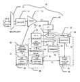
- FIG. 1 is a block diagram of an optical duobinary transmitter in accordance with an embodiment of the present invention
- FIG. 2 is a block diagram showing the configuration of the bias control circuit in FIG. 1 ;
- FIG. 3 is an explanatory diagram illustrating the relationship between the bias voltage V B of an optical duobinary LN-MZ modulator and the optical output power P;
- FIG. 4 is an explanatory diagram illustrating the change in the average value ⁇ P> of the optical output power P in the case where the driving amplitude is modified in an optical duobinary LN-MZ modulator, wherein the bias voltage V B matches the voltage value at which the optical output power P is at a minimum (i.e., the null point of the characteristic transmission curve);
- FIG. 5 is an explanatory diagram illustrating the change in the average value ⁇ P> of the optical output power P in the case where the driving amplitude is modified in an optical duobinary LN-MZ modulator, wherein the bias voltage V B matches the voltage value at which the optical output power P is at a maximum (i.e., the peak of the characteristic transmission curve);
- FIG. 6 is an explanatory diagram illustrating the change in the average value ⁇ P> of the optical output power P in the case where the driving amplitude is modified in an optical duobinary LN-MZ modulator, wherein the bias voltage V B is shifted one-fourth of a period away from the voltage value at which the optical output power P is at a minimum (i.e., the null point of the characteristic transmission curve);
- FIG. 7 is a diagram illustrating the change in the average value ⁇ P> of the optical output power P as a signed quantity resulting in a function of an intermediate value V 0 (i.e., the bias voltage V B ) of an input voltage V;
- FIG. 8 is a diagram illustrating the waveforms of the signals output by the respective components of the device shown in FIG. 1 , in accordance with a first embodiment of the invention
- FIG. 9 is a flowchart of the operations conducted by the device shown in FIG. 1 , in accordance with a first embodiment of the invention.
- FIG. 10 is a diagram illustrating the waveforms of the signals output by the respective components of the device shown in FIG. 1 , in accordance with a second embodiment of the invention.
- FIG. 11 is a flowchart of the operations conducted by the device shown in FIG. 1 , in accordance with a second embodiment of the invention.
- FIG. 1 shows the configuration of an optical duobinary transmitter in accordance with the first embodiment.
- FIG. 2 shows the detailed configuration of the bias control circuit shown in FIG. 1 .
- FIG. 8 illustrates the signal waveforms and timings for each component of the optical duobinary transmitter in accordance with the first embodiment.
- Reference symbols (a) through (h) in FIGS. 1 and 2 correspond to the reference symbols indicating the signals shown in FIG. 8 .
- the optical duobinary transmitter shown in FIG. 1 is provided with the following.
- a modulated signal generator subsystem 10 functions as means for converting a data signal to a three-level duobinary signal (d).
- An optical signal modulator subsystem 20 functions as means for generating a three-level optical duobinary signal by modulating an optical signal using the three-level duobinary signal converted by the modulated signal generator subsystem 10 .
- An optical detector subsystem 30 functions as means for detecting a low-frequency amplitude value (g) by monitoring the output from the optical signal modulator subsystem 20 .
- a bias controller subsystem 40 functions as means for controlling a bias voltage V B that is applied to the optical signal modulator subsystem 20 .
- a low-frequency amplitude modulator subsystem 50 functions as means for modulating the three-level duobinary signal (d) that was converted by the modulated signal generator subsystem 10 by using a low-frequency signal (a).
- the low-frequency amplitude modulator subsystem 50 includes a low-frequency signal generator 51 and a driving amplitude adjustment circuit 52 .
- the low-frequency signal generator 51 generates a low-frequency signal (a).
- the low-frequency signal generator 51 then outputs the generated low-frequency signal (a) to the driving amplitude adjustment circuit 52 .
- the low-frequency signal (a) generated in the first embodiment is a signal having high values and low values.
- the driving amplitude adjustment circuit 52 receives the low-frequency signal (a), generates a pilot tone, and then supplies this pilot tone to the gain control terminal of a driver 13 , to be hereinafter described. Using this pilot tone, the low-frequency signal (a) is amplitude modulated onto the output signal (c) from the driver 13 .
- the low-frequency signal generator 51 also supplies the low-frequency signal (a) to the bias controller subsystem 40 .
- the optical signal modulator subsystem 20 includes a CW laser diode 21 that emits CW laser light, as well as a single-drive LN-MZ modulator 22 that modulates the light from the CW laser diode 21 .
- LN-MZ modulator 22 light from the CW laser diode 21 is modulated, an optical duobinary signal is generated, and this signal is then output from an optical output terminal 23 .
- the modulated signal generator subsystem 10 includes a multiplexer 11 , a precoder 12 , a driver 13 , a low-pass filter 14 , a bias tee 15 , and a terminator 16 .
- a data signal and a clock signal from outside the transmitter are input, and a serial data signal is generated.
- the serial data signal generated in the multiplexer 11 and the clock signal are then input into the precoder 12 , where the signals are differentially encoded.
- the internal configuration of the precoder 12 may be as disclosed by W. Kaiser et al., for example.
- the output of the precoder 12 is connected to the driver 13 .
- the driver 13 is provided with a gain adjustment terminal, and the low-frequency signal (a) modulated onto amplitude of the output signal (c) from the driver 13 by using the pilot tone input from the driving amplitude adjustment circuit 52 .
- This modulation of the output signal (c) from the driver 13 by the low-frequency signal (a) is conducted in order to detect the optimal set value for the bias voltage V B .
- the output signal (c) from the driver 13 is filtered and then converted into a three-level duobinary signal (d) at the low-pass filter 14 .
- the three-level duobinary signal (d) converted at the low-pass filter 14 is then input into the LN-MZ modulator 22 (i.e., the optical modulator).
- the LN-MZ modulator 22 Upon receiving as input the three-level duobinary signal (d), the LN-MZ modulator 22 modulates the light from the CW laser diode 21 , and generates a three-level optical duobinary signal.
- the principles of optical duobinary signal generation are already known, as described in detail in Japan Patent No. 3306573, for example.
- the dual-drive LN-MZ modulator used in the above literature is not used, and instead a single-drive LN-MZ modulator is used.
- the three-level duobinary signal (d) input into the LN-MZ modulator 22 passes through the bias tee 15 and is terminated at the terminator 16 .
- the bias tee 15 includes an inductance element 151 and a capacitor 152 .
- the capacitor 152 is positioned between the LN-MZ modulator 22 and the terminator 16 , while one end of the inductance element 151 is connected to a connection wire running between the capacitor 152 and the LN-MZ modulator 22 .
- the other end of the inductance element 151 is connected to the output of a bias generator circuit 45 .
- the bias tee 15 couples the bias generator circuit 45 and the LN-MZ modulator 22 .
- the bias tee 15 is used for terminating the three-level duobinary signal (d) and applying the bias voltage V B .
- other methods may also be implemented, so long as they provide means to terminate the three-level duobinary signal (d) while maintaining the application of a bias voltage V B to the LN-MZ modulator 22 .
- a method may be used wherein independent electrodes are provided for applying a bias voltage V B to the LN-MZ modulator 22 .
- the bias tee 15 is disposed between the LN-MZ modulator 22 and the terminator 16 , but the invention is not limited thereto.
- a configuration wherein the bias tee 15 is disposed between the low-pass filter 14 and the LN-MZ modulator 22 is also possible.
- the optical detector subsystem 30 includes an optical coupler 31 , a monitor PD 32 , and an optical power detector circuit 33 .
- the optical coupler 31 is disposed between the LN-MZ modulator 22 and the optical output terminal 23 .
- the optical coupler 31 partially splits the optical duobinary signal and sends the signal to the monitor PD 32 .
- the monitor PD 32 is a light-detecting element having for example light-sensitive spectral characteristics and response characteristics capable of detecting the optical duobinary signal, and may be constructed from a photodiode, for example.
- the monitor PD 32 receives the optical duobinary signal that was split from the optical coupler 31 , detects the light intensity (i.e., the optical output power) of the optical duobinary signal, and then converts the detected optical output power into a corresponding electrical signal.
- the monitor PD 32 is connected to the optical power detector circuit 33 , and inputs the converted electrical signal corresponding to the optical output power into the optical power detector circuit 33 .
- LN-MZ modulator modules that include a built-in monitor PD that detects optical output power.
- Such LN-MZ modulator modules with built-in monitor PDs may be used in lieu of the LN-MZ modulator 22 , the optical coupler 31 , and the monitor PD 32 .
- the monitor PD 32 is often configured to detect light that leaks from the LN-MZ modulator 22 .
- the characteristic transmission curve of the monitor PD is the reverse of the characteristic transmission curve of the optical output of the LN-MZ modulator. For this reason, it is necessary to invert the polarity of detecting the optical output power.
- the optical power detector circuit 33 takes the converted electrical signal corresponding to the optical output power that was detected by the monitor PD 32 , converts this electrical signal from analog to digital, and then outputs the result as a monitor output signal (f).
- a transimpedance amp for example, may be used as the optical power detector circuit 33 .
- the bias controller subsystem 40 includes a low-frequency component detector 43 , a bias controller circuit 44 , and a bias generator circuit 45 .
- the low-frequency component detector 43 reads the values of the monitor output signal (f) output from the optical power detector 33 , and detects the amplitude values of the low-frequency signal (a) in the monitor output signal (f).
- the low-frequency component detector 43 calculates the difference (VH ⁇ VL) between the value VH of the monitor output signal (f) when the low-frequency signal (a) is high, and the signal value VL of the monitor output signal (f) when the low-frequency signal (a) is low. Subsequently, the low-frequency component detector 43 outputs the detected amplitude values (VH ⁇ VL) of the low-frequency signal (a) as a low-frequency amplitude signal (g). This low-frequency amplitude signal (g) is then input into a dither component detector 442 provided in the bias controller circuit 44 , to be hereinafter described.
- FIG. 2 shows the internal configuration of the bias controller circuit 44 , which will now be described with reference to FIG. 2 .
- the bias controller circuit 44 includes a dither generator 441 , a dither component detector 442 , a bias value calculator 443 , and an adder 444 .
- the dither generator 441 generates a dither signal (b), and then outputs the generated dither signal (b) to the dither component detector 442 and the adder 444 .
- the dither signal (b) refers to a signal having dither bias voltage values of ⁇ Vb when the set bias value is Vb.
- the dither component detector 442 Upon receiving as input the low-frequency amplitude signal (g) from the low-frequency component detector 43 , the dither component detector 442 refers to the dither signal (b) input from the dither generator 441 , and thereby detects the amplitude values of the dither signal (b) in the low-frequency amplitude signal (g).
- the detected amplitude values of the dither signal (b) are then output as a dither amplitude signal (h), this signal being input into the bias value calculator 443 .
- the bias value calculator 443 calculates a correction value for the set bias value Vb on the basis of the dither amplitude signal (h) output from the dither component detector 442 .
- the bias value calculator 443 then outputs a new set bias value Vb to the adder 444 .
- the adder 444 Upon receiving both the new set bias value Vb that was calculated by the bias value calculator 443 , as well as the dither signal (b) generated by the dither generator 441 , the adder 444 outputs a signal (e) that takes the combined voltage (Vb ⁇ Vb) of the new set bias voltage value Vb and the dither bias voltage value ⁇ Vb to be the bias voltage V B , and then outputs this signal (e) to the bias generator circuit 45 .
- the low-frequency signal (a) output from the low-frequency signal generator 51 is shown in FIG. 8( a ).
- the low-frequency signal (a) in the first embodiment is a signal having high and low values.
- the low-frequency signal (a) is a signal having high and low values
- the signal may be a sine wave or a rectangular wave.
- the low-frequency signal generator 51 outputs the low-frequency signal (a) to the driving amplitude adjustment circuit 52 .
- the driving amplitude adjustment circuit 52 receives the low-frequency signal (a), generates a pilot tone, and supplies this tone to the gain control terminal of the driver 13 .
- the low-frequency signal (a) is amplitude modulated onto the output signal (c) of the driver 13 .
- the output signal (c) of the driver 13 is shown in FIG. 8( c ).
- the output signal (c) of the driver 13 is input into the low-pass filter 14 .
- the output signal (c) of the driver 13 is converted into the three-level duobinary signal (d).
- the three-level duobinary signal (d) converted in the low-pass filter (LPF) 14 is then input into the LN-MZ modulator 22 .
- the three-level duobinary signal (d) converted in the low-pass filter (LPF) 14 is shown in FIG. 8( d ).
- the dither generator 441 within the bias controller circuit 44 generates a dither signal (b), and outputs the generated dither signal (b) to the dither component detector 442 and the adder 444 .
- the dither signal (b) generated by the dither generator 441 is shown in FIG. 8( b ).
- the dotted line in FIG. 8( b ) indicates the value of the set bias value Vb, while the solid line indicates the dither signal (b) output by the dither generator 441 .
- the dither bias voltage values are ⁇ Vb with respect to the set bias value Vb.
- the adder 444 Upon receiving as input both the new set bias value Vb calculated by the bias value calculator 443 as well as the dither signal (b) generated by the dither generator 441 , the adder 444 output a signal (e) that takes the combined voltage (Vb ⁇ Vb) of the new set bias value Vb and the dither bias voltage value ⁇ Vb to be the bias voltage V B , and then outputs this signal (e) to the bias generator circuit 45 .
- the signal (e) that takes (Vb ⁇ Vb) to be the bias voltage V B is shown in FIG. 8( e ). The broken line in FIG.
- the bias voltage V B (Vb ⁇ Vb) is applied to the LN-MZ modulator 22 .
- the LN-MZ modulator 22 modulates the light from the CW laser diode 21 , and generates an optical duobinary signal.
- the optical duobinary signal generated by the LN-MZ modulator 22 is then input into the monitor PD 32 via the optical coupler 31 .
- the monitor PD 32 detects the optical output power of the optical duobinary signal, converts the detected optical output power into a corresponding electrical signal, and then outputs this electrical signal to the optical power detector 33 .
- the optical power detector 33 converts the electrical signal input from the monitor PD 32 from analog to digital, and then outputs the digital signal as the monitor output signal (f).
- the monitor output signal (f) output by the optical power detector 33 is shown in FIG. 8( f ).
- the low-frequency component detector 43 detects the amplitude values of the next low-frequency signal (a) in the monitor output signal (f) output by the optical power detector 33 ( FIG. 8( f )). The low-frequency component detector 43 then outputs the amplitude values of the detected low-frequency signal (a) as a low-frequency amplitude signal (g), and outputs this low-frequency amplitude signal (g) to the dither component detector 442 within the bias controller circuit 44 .
- the low-frequency amplitude signal (g) output by the low-frequency component detector 43 is shown in FIG. 8( g ).
- the dither component detector 442 then refers to the dither signal (b) input from the dither generator 441 , and solves for the amplitude values of the dither signal (b) in the low-frequency amplitude signal (g).
- the dither component detector 442 outputs the calculated amplitude values of the dither signal (b) as a dither signal amplitute (h), and outputs this signal to the bias value calculator 443 within the bias controller circuit 44 .
- the dither signal amplitute (h) output by the dither component detector 442 is shown in FIG. 8( h ).
- optical transmitter using optical duobinary modulation operating as described above in accordance with an embodiment of the present invention will now be described in further detail, including description of the operational principles thereof.
- the relationship between the three-level input voltage V input into the LN-MZ modulator 22 and the optical output power P of the LN-MZ modulator 22 is as shown in FIG. 3 . Moreover, the optical output power P becomes a periodic function of the input voltage V.
- the intermediate voltage value V 0 of the three-level input voltage V input into the LN-MZ modulator 22 is configured to match the voltage value where the optical output power P of the LN-MZ modulator 22 is at a minimum (i.e., the null point of the characteristic transmission curve).
- the bias voltage V B is configured to match the voltage value where the optical output power P of the LN-MZ modulator 22 is at a minimum (i.e., the null point of the characteristic transmission curve).
- FIG. 4 shows the change in the average value ⁇ P> of the optical output power P due to changes in the driving amplitude VRF, wherein the intermediate voltage V 0 (i.e., the bias voltage V B ) of the input voltage V matches the voltage value where the optical output power P is at a minimum (i.e., the null point of the characteristic transmission curve).
- V 0 i.e., the bias voltage V B
- FIG. 5 shows the change in the average value ⁇ P> of the optical output power P due to changes in the driving amplitude VRF, wherein the intermediate voltage V 0 (i.e., the bias voltage V B ) of the input voltage V matches the voltage value where the optical output power P is at a maximum (i.e., the peak of the characteristic transmission curve).
- V 0 i.e., the bias voltage V B
- FIG. 6 shows the change in the average value ⁇ P> of the optical output power P due to changes in the driving amplitude VRF, wherein the intermediate voltage V 0 (i.e., the bias voltage V B ) of the input voltage V matches a voltage value shifted one-fourth of a period away from the voltage value where the optical output power P is at a minimum (i.e., the null point of the characteristic transmission curve).
- V 0 i.e., the bias voltage V B
- ⁇ P 1 > and ⁇ P 2 > represent the average value ⁇ P> of the optical output power P in the case where the driving amplitude VRF of the input voltage V input into the LN-MZ modulator 22 is V 1 and V 2 , respectively (herein, V 1 >V 2 ).
- the average value ⁇ P> of the optical output power P changes from ⁇ P 2 > to ⁇ P 1 >, and thus the average value ⁇ P> of the optical output power P increases.
- ⁇ P 1 > and ⁇ P 2 > represent the average value ⁇ P> of the optical output power P in the case where the driving amplitude VRF of the input voltage V input into the LN-MZ modulator 22 is V 1 and V 2 , respectively (herein, V 1 >V 2 ).
- ⁇ P 1 > and ⁇ P 2 > represent the average value ⁇ P> of the optical output power P in the case where the driving amplitude VRF of the input voltage V input into the LN-MZ modulator 22 is V 1 and V 2 , respectively (herein, V 1 >V 2 ).
- the intermediate voltage V 0 i.e., the bias voltage V B
- the intermediate voltage V 0 i.e., the bias voltage V B
- the intermediate voltage V 0 i.e., the bias voltage V B
- the characteristic transmission curve of the LN-MZ modulator 22 becomes an odd function centered about the intermediate value V 0 (i.e., the bias voltage V B ) of the input voltage V. For this reason, changes in the average value ⁇ P> of the optical output power P due to changes in the driving amplitude VRF are counterbalanced about the intermediate value V 0 (i.e., the bias voltage V B ) of the input voltage V.
- the average value ⁇ P> of the optical output power P changes when the driving amplitude VRF changes. Furthermore, it can be seen that the change in the average value ⁇ P> of the optical output power P is different according to the intermediate value V 0 (i.e., the bias voltage V B ) of the input voltage V with respect to the voltage value where the optical output power P is at a minimum (i.e., the null point of the characteristic transmission curve).
- the average value ⁇ P> of the optical output power P changes as the driving amplitude VRF changes, but the magnitude and the sign (i.e., the sign of the magnitude) of the change is dependent upon the intermediate value V 0 (i.e., the bias voltage V B ) of the input voltage V with respect to the voltage value where the optical output power P is at a minimum (i.e., the null point of the characteristic transmission curve).
- the amount of change in the average value ⁇ P> of the optical output power P is taken to be a signed quantity, and is shown as a function of the intermediate value V 0 (i.e., the bias voltage V B ) of the input voltage V in FIG. 7 .
- the dotted line in FIG. 7 indicates the characteristic transmission curve of the optical output power P of the LN-MZ modulator 22 .
- the solid line in FIG. 7 indicates the amount of change in the average value ⁇ P> of the optical output power P when the driving amplitude VRF is increased. From FIG.
- the bias voltage V B is controlled such that the amount of change in the average value ⁇ P> of the optical output power P is maximized when the driving amplitude VRF is increased, then the intermediate value V 0 (i.e., the bias voltage V B ) of the input voltage value V will match the voltage value where the optical output power P is at a minimum (i.e., the null point of the characteristic transmission curve).
- the driving amplitude VRF is first modified by the low-frequency signal (a), and then the average value ⁇ P> of the optical output power P is detected using the monitor PD 32 . Subsequently, by retrieving the amplitude values of the low-frequency signal (a) in the average value ⁇ P> of the optical output power P, the amount of change in the average value ⁇ P> of the optical output power P due to the driving amplitude VRF is detected as a signed quantity.
- a dither voltage ⁇ V B from a dither signal (b) is superimposed on the bias voltage V B applied to the LN-MZ modulator 22 .
- the bias voltage V B can be controlled such that the voltage value where the optical output power P is at a minimum (i.e., the null point of the characteristic transmission curve) and the intermediate value V 0 (i.e., the bias voltage V B ) of the input voltage V match.
- the optical output power P can be expressed as a periodic function of the input voltage V as shown in FIG. 3 :
- Pmax is the maximum value of the optical output power P.
- the minimum value Pmin of the optical output power is taken to be 0.
- a single period of P(V) is taken to be 2V ⁇ ⁇ .
- Equation (1) yields the following when the input voltage V is taken to be V 0 ⁇ VRF/2, V 0 , and V 0 +VRF/2, respectively.
- P ⁇ ( V 0 - V RF 2 ) P max 2 ⁇ ( cos ⁇ ⁇ V 0 - V RF 2 V ⁇ ⁇ ⁇ + 1 ) ( 2 )
- P ⁇ ( V 0 ) P max 2 ⁇ ( cos ⁇ ⁇ V 0 V ⁇ ⁇ ⁇ + 1 ) ( 3 )
- P ⁇ ( V 0 + V RF 2 ) P max 2 ⁇ ( cos ⁇ ⁇ V 0 + V RF 2 V ⁇ ⁇ ⁇ + 1 ) ( 4 )
- the average value ⁇ P> of the optical output power P will be solved for, but before that, the event probability of an input signal V input into the LN-MZ modulator 22 and having values of (V 0 ⁇ VRF/2, V 0 , V 0 +VRF/2) will be described.
- the signal is assigned a logical value of 0 when the input voltage V is V 0 , while the signal is assigned a logical value of 1 when the input voltage V is V 0 ⁇ VRF/2 or V 0 +VRF/2.
- the mark ratio of both a logical 0 and a logical 1 is assumed to be 50%.
- the event frequency is 1 ⁇ 2 for a signal wherein the input voltage V is V 0
- the event frequency is 1 ⁇ 4 for a signal wherein the input voltage V is V 0 ⁇ (VRF/2)
- the event frequency is 1 ⁇ 4 for a signal wherein the input voltage V is V 0 +(VRF/2).
- the value of the input voltage V input into the LN-MZ modulator 22 has a 1 ⁇ 2 probability of being V 0 , a 1 ⁇ 4 probability of being V 0 ⁇ (VRF/2), and a 1 ⁇ 4 probability of being V 0 +(VRF/2).
- the input voltage V exhibits the following voltage values at the following respective probabilities.
- a signal wherein the value of the input voltage V is V 0 ⁇ (VRF/2) occurs at a probability of 1 ⁇ 4;
- the input voltage V exhibits the following voltage values at the following respective probabilities.
- a signal wherein the value of the input voltage V is V 0 ⁇ (VRF/2) occurs at a probability of 1 ⁇ 8;
- a signal wherein the value of the input voltage V is V 0 ⁇ (VRF/2) (t/ts) occurs at a probability of 1 ⁇ 8;
- the input voltage V takes the respective voltage values at the probabilities described above, and is input into the LN-MZ modulator 22 .
- the average value ⁇ P> of the optical output power P can be expressed as a function of V 0 and VRF:
- VRF is set such that VRF is approximately equal to 2V ⁇ ⁇ , and thus m is approximately equal to 1. Consequently, equation (7) becomes
- the amplitude modulation of the low-frequency signal (a) onto the output signal (c) of the driver 13 is equivalent to changing the amplitude (driving amplitude) VRF of the input voltage V in FIG. 3 .
- the calculation of the amplitude values for the low-frequency signal (a) in the electrical signal corresponding to the optical output power P detected by the monitor PD 32 is equivalent to calculating the amount of change in the average value ⁇ P> of the optical output power P in accordance with the amount of change in VRF.
- equation (8) since m is approximately equal to VRF/2V ⁇ , calculating the amount of change in the average value ⁇ P> of the optical output power P in accordance with the amount of change in m is equivalent to calculating the amount of change in the average value ⁇ P> of the optical output power P in accordance with the amount of change in VRF.
- equation (8) is equivalent to the solid line in FIG. 7 .
- V 0 in case of controlling V 0 to be at the null point of the characteristic transmission curve, one need only control V 0 (i.e., the bias voltage V B ) such that the low-frequency amplitude value for the average value ⁇ P> of the optical output power P in accordance with the change in VRF is maximized.
- the respective constituent elements shown in FIG. 1 are assumed to be configured using dedicated hardware.
- all or part of the configuration of the bias controller subsystem 40 may be realized by a computer system.
- software may be installed on a computer system having a central processing unit (CPU), memory, interface circuits, and similar components.
- CPU central processing unit
- memory volatile and re-writable memory
- interface circuits and similar components.
- concrete means for realizing the functions of the respective circuits shown in FIG. 1 are realized.
- an example will be described wherein the low-frequency component detector 43 and the bias controller circuit 44 in the bias controller subsystem 40 shown in FIG. 1 are realized by a computer.
- the bias controller circuit 44 sets the set bias value Vb that constitutes the bias voltage V B applied to the LN-MZ modulator 22 (step S 100 ). Initially, however, the initial value for the set bias value Vb is set by processing input received via an input device (not shown in the drawings). Alternatively, a value stored in advance in ROM or similar memory (not shown in the drawings) within the bias controller circuit 44 may be set as the initial value for Vb. In this case, the initial value is stored in ROM or similar memory within the bias controller circuit 44 during the product shipping stage. Subsequently, when power to the bias controller circuit 44 is switched on, the bias controller circuit 44 reads the initial value from the ROM and sets the read initial value as the set bias value Vb.
- the bias controller circuit 44 outputs to the bias generator circuit 45 the value (Vb ⁇ Vb) obtained by adding the dither bias voltage ( ⁇ Vb) to the set bias value Vb (step S 101 ).
- the state of the low-frequency signal (a) input from the low-frequency signal generator 51 is determined to be high or low.
- the value VH of the monitor output signal (f) is read from the optical power detector 33 (step S 102 ).
- the value VL of the monitor output signal (f) is read from the optical power detector 33 (step S 103 ).
- An average value for V ⁇ mon may also be solved for by performing plural repetitions of the processing in steps S 102 to S 104 .
- the bias controller circuit 44 outputs to the bias generator circuit 45 the value (Vb+ ⁇ Vb) obtained by adding the dither bias voltage (+ ⁇ Vb) to the set bias value Vb (step S 105 ).
- the state of the low-frequency signal (a) input from the low-frequency signal generator 51 is determined to be high or low.
- the value VH of the monitor output signal (f) is read from the optical power detector 33 (step S 106 ).
- the value VL of the monitor output signal (f) is read from the optical power detector 33 (step S 107 ).
- An average value for V+mon may also be solved for by performing plural repetitions of the processing in steps S 106 to S 108 .
- step S 100 the current set bias value Vb is replaced by the new set bias value Vb′.
- the above process is then subsequently repeated.
- the dither signal amplitute (h) progressively and asymptotically approaches 0 (as indicated by the broken line).
- the bias voltage V B asymptotically approaches the set bias value Vb.
- a low-frequency signal (a) having high and low values is amplitude modulated onto the output signal (c) of the driver 13 , thereby modifying the amplitude (driving amplitude) VRF of the input voltage V input into the LN-MZ modulator 22 .
- a low-frequency signal (a), having high, low, and middle values as shown in FIG. 10( a ), is amplitude modulated onto the output signal (c) of the driver 13 , thereby modifying the amplitude (driving amplitude) VRF of the input voltage V input into the LN-MZ modulator 22 .
- optical duobinary transmitter of the second embodiment is similar to that of the first embodiment, and hereinafter only the differences therebetween will be described.
- the low-frequency signal generator 51 of the low-frequency amplitude modulator subsystem 50 outputs a low-frequency signal (a) having high, low, and middle values, as shown in FIG. 10( a ).
- the low-frequency component detector 43 first reads the value of the monitor output signal (f) output by the optical power detector 33 . Upon detecting the amplitude values of the low-frequency signal (a) in the monitor output signal (f), the low-frequency component detector 43 calculates the value (VH+VL ⁇ 2VM) by subtracting twice the value VM of the monitor output signal (f) when the low-frequency signal (a) is middle from the sum of the value VH of the monitor output signal (f) when the low-frequency signal (a) is high and the value VL of the monitor output signal (f) when the low-frequency signal (a) is low. Subsequently, the amplitude value (VH+VL ⁇ 2VM) of the detected low-frequency signal (a) is output as a low-frequency amplitude signal (g).
- the operation of the components constituting the optical duobinary transmitter in accordance with the second embodiment will now be described with reference to the timing chart in FIG. 10 .
- the reference symbols indicating the signals shown in FIG. 10 correspond to the reference symbols (a) through (h) in FIGS. 1 and 2 .
- the low-frequency signal (a) output from the low-frequency signal generator 51 in the second embodiment is shown in FIG. 10( a ).
- the low-frequency signal (a) in the second embodiment is a signal having high, low, and middle values, as shown in FIG. 10( a ).
- a signal like that shown in FIG. 10( a ) may also be generated by a method wherein two rectangular waves having identical frequencies but out of phase with each other are superimposed in a summing amplifier.
- the low-frequency signal (a) in the second embodiment need not be a stepped signal as shown in FIG. 10( a ), but may any signal having high, low, and middle values.
- a wave may be used that gradually transitions between high, middle, and low values.
- the low-frequency signal generator 51 outputs the low-frequency signal (a) to the driving amplitude adjustment circuit 52 .
- the driving amplitude adjustment circuit 52 receives the low-frequency signal (a), generates a pilot tone, and supplies this tone to the gain control terminal of the driver 13 .
- the low-frequency signal (a) is amplitude modulated onto the output signal (c) of the driver 13 .
- the output signal (c) of the driver 13 is shown in FIG. 10( c ).
- the output signal (c) of the driver 13 is then input into a low-pass filter 14 .
- the output signal (c) of the driver 13 is converted into a three-level duobinary signal (d).
- the three-level duobinary signal (d) converted at the low-pass filter (LPF) 14 is then input into the LN-MZ modulator 22 .
- the three-level duobinary signal (d) converted at the low-pass filter (LPF) 14 is shown in FIG. 10( d ).
- VRF is taken to be the amplitude (driving amplitude) of the three-level duobinary signal (d)
- the dither generator 441 within the bias controller circuit 44 generates a dither signal (b), and outputs the generated dither signal (b) to the dither component detector 442 and the adder 444 .
- the dither signal (b) generated by the dither generator 441 is shown in FIG. 10( b ).
- the dotted line in FIG. 10( b ) indicates the value of the set bias value Vb, while the solid line indicates the dither signal (b) output by the dither generator 441 .
- the dither bias voltage values have ⁇ Vb with respect to the set bias value Vb.
- the adder 444 Upon receiving as input both the new set bias value Vb calculated by the bias value calculator 443 as well as the dither signal (b) generated by the dither generator 441 , the adder 444 generates a signal (e) that takes the combined voltage (Vb+ ⁇ Vb) of the new set bias value Vb and the dither bias voltage value ⁇ Vb to be the bias voltage V B , and then outputs this signal (e) to the bias generator circuit 45 .
- the signal (e) that takes (Vb ⁇ Vb) to be the bias voltage V B and output from the adder 444 is shown in FIG. 10( e ). The broken line in FIG.
- the bias voltage V B (Vb ⁇ Vb) is applied to the LN-MZ modulator 22 .
- the LN-MZ modulator 22 modulates the light from the CW laser diode 21 , and generates an optical duobinary signal.
- the optical duobinary signal generated by the LN-MZ modulator 22 is then input into the monitor PD 32 via the optical coupler 31 .
- the monitor PD 32 detects the optical output power of the optical duobinary signal, converts the detected optical output power into a corresponding electrical signal, and then outputs this electrical signal to the optical power detector 33 .
- the optical power detector 33 converts the electrical signal input from the monitor PD 32 from analog to digital, and then outputs the digital signal as the monitor output signal (f).
- the monitor output signal (f) output by the optical power detector 33 is shown in FIG. 10( f ).
- the low-frequency component detector 43 detects the amplitude values of the next low-frequency signal (a) in the monitor output signal (f) output by the optical power detector 33 ( FIG. 10( f )). The low-frequency component detector 43 then outputs the amplitude values of the detected low-frequency signal (a) as a low-frequency amplitude signal (g), and outputs this low-frequency amplitude signal (g) to the dither component detector 442 within the bias controller circuit 44 .
- the value (VH+VL ⁇ 2VM) is obtained by subtracting twice the value VM of the monitor output signal (f) when the low-frequency signal (a) is middle from the sum of the value VH of the monitor output signal (f) when the low-frequency signal (a) is high and the value VL of the monitor output signal (f) when the low-frequency signal (a) is low.
- the value (VH+VL ⁇ 2VM) is obtained by subtracting twice the value VM of the monitor output signal (f) when the low-frequency signal (a) is middle from the sum of the value VH of the monitor output signal (f) when the low-frequency signal (a) is high and the value VL of the monitor output signal (f) when the low-frequency signal (a) is low.
- the low-frequency amplitude signal (g) output by the low-frequency component detector 43 is shown in FIG. 10( g ).
- the dither component detector 442 then refers to the dither signal (b) input from the dither generator 441 , and solves for the amplitude values of the dither signal (b) in the low-frequency amplitude signal (g).
- the dither component detector 442 outputs the calculated amplitude values of the dither signal (b) as a dither signal amplitute (h), and outputs this signal to the bias value calculator 443 within the bias controller circuit 44 .
- the dither signal amplitute (h) output by the dither component detector 442 is shown in FIG. 10( h ).
- the low-frequency component detector 43 evaluates VH+VL ⁇ 2VM to solve for the amplitude values of the low-frequency signal (a). In other words, the low-frequency component detector 43 solves for the value obtained by subtracting twice the value VM of the monitor output signal (f) when the low-frequency signal (a) is middle from the sum of the value VH of the monitor output signal (f) when the low-frequency signal (a) is high and the value VL of the monitor output signal (f) when the low-frequency signal (a) is low.
- VH+VL ⁇ 2VM will be described with the use of equations.
- the respective constituent elements shown in FIG. 1 are assumed to be configured using dedicated hardware.
- all or part of the configuration of the bias controller subsystem 40 may be realized by a computer system.
- software may be installed on a computer system having a central processing unit (CPU), memory, interface circuits, and similar components.
- CPU central processing unit
- a computer functions as the low-frequency component detector 43 and the bias controller circuit 44 .
- the bias controller circuit 44 sets the set bias value Vb that constitutes the bias voltage V B applied to the LN-MZ modulator 22 (step S 200 ). Initially, however, the initial value for the set bias value Vb is input by processing receipt via an input device (not shown in the drawings). Alternatively, a value stored in advance in ROM or similar memory (not shown in the drawings) within the bias controller circuit 44 may be set as the initial value for Vb. In this case, the initial value is stored in ROM or similar memory within the bias controller circuit 44 during the product shipping stage. Subsequently, when power to the bias controller circuit 44 is switched on, the bias controller circuit 44 reads the initial value from the ROM and sets the read-out initial value as the set bias value Vb.
- the bias controller circuit 44 outputs to the bias generator circuit 45 the value (Vb ⁇ Vb) obtained by adding the dither bias voltage ( ⁇ Vb) to the set bias value Vb (step S 201 ).
- the state of the low-frequency signal (a) input from the low-frequency signal generator 51 is determined to be high, low, or middle.
- the value VH of the monitor output signal (f) is read from the optical power detector 33 (step S 202 ).
- the value VL of the monitor output signal (f) is read from the optical power detector 33 (step S 203 ).
- the value VM of the monitor output signal (f) is read from the optical power detector circuit 33 (step S 204 ).
- An average value for V ⁇ mon′ may also be solved for by performing plural repetitions of the processing in steps S 202 to S 205 .
- the bias controller circuit 44 outputs to the bias generator circuit 45 the value (Vb+ ⁇ Vb) obtained by adding the dither bias voltage (+ ⁇ Vb) to the set bias value Vb (step S 206 ).
- the state of the low-frequency signal (a) input from the low-frequency signal generator 51 is determined to be high, low, or middle.
- the value VH of the monitor output signal (f) is read from the optical power detector 33 (step S 207 ).
- the value VL of the monitor output signal (f) is read from the optical power detector 33 (step S 208 ).
- the value VM of the monitor output signal (f is read from the optical power detector circuit 33 (step S 209 ).
- An average value for V+mon′ may also be solved for by performing plural repetitions of the processing in steps S 207 to S 210 .
- step S 200 the current set bias value Vb is replaced by the new set bias value Vb′.
- the above process is then subsequently repeated.
- the dither signal amplitude (h) progressively and asymptotically approaches 0 (as indicated by the broken line).
- the bias voltage V B asymptotically approaches the set bias value Vb.
- the value of the difference V+mon′ and V ⁇ mon′ in the monitor output signal (f) may be evaluated by reading the value VM twice from the optical power detector circuit 33 when the low-frequency signal (a) goes middle, and then evaluating VH+VL ⁇ VM ⁇ VM′.
- the value of the first reading of the monitor output signal (f) is taken to be VM
- the value of the second reading of the monitor output signal (f) is taken to be VM′.
- the control loop of the bias voltage V B is reversed, while maintaining the same configuration of the optical duobinary transmitters in accordance with the first and the second embodiments.
- the intermediate value V 0 i.e., the bias voltage V B
- the bias voltage V B the input voltage V input into the LN-MZ modulator 22 is controlled so as to match the voltage value where the optical output power P of the LN-MZ modulator 22 is at a maximum (i.e., the peak of the characteristic transmission curve), as shown in FIG. 5 .
- an input voltage V is input into the LN-MZ modulator 22 , being centered about the voltage value where the optical output power P of the LN-MZ modulator 22 is at a minimum (i.e., the null point of the characteristic transmission curve), as shown in FIG. 4 .
- the phase of the characteristic transmission curve of the LN-MZ modulator 22 is 0° or 180°, a very strong signal is obtained.
- an input voltage V is input into the LN-MZ modulator 22 that is centered about the voltage value where the optical output power P of the LN-MZ modulator 22 is at a maximum (i.e., the peak of the characteristic transmission curve), as shown in FIG. 5 .
- a strong signal is obtained only when the phase of the characteristic transmission curve of the LN-MZ modulator 22 is 90°.
- the optical signal generated by the LN-MZ modulator 22 is a binary signal similar to the binary IM optical transmitters of the related art.
- a signal similar to a binary IM signal i.e., a binary signal
- V B the bias voltage
- the logical values of the optical duobinary signal output from the LN-MZ modulator 22 in the case of FIG. 5 can be made identical to the logical values of the optical duobinary signal output from the LN-MZ modulator 22 in the case of FIG. 4 .
- typical, commercially-available multiplexers 11 have functions to reverse output logical values.
- the present invention enables automatic bias control of an optical duobinary transmitter using a single-drive LN-MZ modulator. In so doing, null point drift in the LN-MZ modulator is compensated for, and an optical duobinary transmitter is realized that operates stably over long periods of time.
Abstract
Description
Taking the partial derivative of equation (6) with respect to m yields
In optical duobinary modulation, VRF is set such that VRF is approximately equal to 2Vπ−, and thus m is approximately equal to 1. Consequently, equation (7) becomes
equation (9) becomes equal to
It can be seen from equation (11) that evaluating VH+VL−2VM is equivalent to solving for the amount of second-order change in the monitor output signal (f) (i.e., the average value <P> of the optical output power P) due to VRF.
holds true, wherein m=VRF/Vπ− and b=V0/Vπ−. Taking the second-order partial derivative of equation (12) with respect to m yields
Claims (5)
Applications Claiming Priority (4)
| Application Number | Priority Date | Filing Date | Title |
|---|---|---|---|
| JP2007113436 | 2007-04-23 | ||
| JP2007-113436 | 2007-04-23 | ||
| JP2008-083719 | 2008-03-27 | ||
| JP2008083719A JP4971230B2 (en) | 2007-04-23 | 2008-03-27 | Optical transmitter |
Publications (2)
| Publication Number | Publication Date |
|---|---|
| US20090060528A1 US20090060528A1 (en) | 2009-03-05 |
| US8098998B2 true US8098998B2 (en) | 2012-01-17 |
Family
ID=40167717
Family Applications (1)
| Application Number | Title | Priority Date | Filing Date |
|---|---|---|---|
| US12/108,089 Active 2030-10-30 US8098998B2 (en) | 2007-04-23 | 2008-04-23 | Optical transmitter |
Country Status (2)
| Country | Link |
|---|---|
| US (1) | US8098998B2 (en) |
| JP (1) | JP4971230B2 (en) |
Cited By (3)
| Publication number | Priority date | Publication date | Assignee | Title |
|---|---|---|---|---|
| US9319145B2 (en) | 2012-03-22 | 2016-04-19 | Nec Corporation | Optical transmitter, optical transmission/reception system, and drive circuit |
| US10191306B2 (en) | 2015-02-18 | 2019-01-29 | Oclaro Technology Limited | Dither free bias control |
| US11385517B1 (en) * | 2016-11-23 | 2022-07-12 | Eospace Inc. | Dual polarization optical modulator with independent phase tuning for each polarization state and its application in an optical integrated circuit architecture for optically-controlled RF phased-array beam forming |
Families Citing this family (16)
| Publication number | Priority date | Publication date | Assignee | Title |
|---|---|---|---|---|
| US7643759B2 (en) * | 2005-01-12 | 2010-01-05 | Sumitomo Electric Industries, Ltd. | Signal-quality evaluation device, signal adjustment method, optical-signal evaluation system, and optical transmission system |
| JP4956842B2 (en) * | 2008-04-23 | 2012-06-20 | Necエンジニアリング株式会社 | Optical transmitter |
| KR101190863B1 (en) * | 2008-12-16 | 2012-10-15 | 한국전자통신연구원 | Optical transmitter for optimizing input dc bias voltage of optical modulator with duo-binary modulation and method thereof |
| US8543010B2 (en) * | 2010-02-24 | 2013-09-24 | Jds Uniphase Corporation | Bias control in an optical modulator and transmitter |
| EP2700178B1 (en) * | 2011-04-19 | 2018-06-27 | Nec Corporation | Optical transmitter and method for controlling the same |
| US20130177316A1 (en) * | 2012-01-06 | 2013-07-11 | Emcore Corporation | Optical communication system, and transmitter and receiver apparatus therefor |
| WO2013140476A1 (en) * | 2012-03-22 | 2013-09-26 | 日本電気株式会社 | Optical transmitter, optical transmission/reception system, and drive circuit |
| CN105099569B (en) * | 2015-06-25 | 2017-12-12 | 北京邮电大学 | The bias control system and method for a kind of Mach of increasing Dare modulator |
| WO2017126546A1 (en) * | 2016-01-21 | 2017-07-27 | 日本電気株式会社 | Optical transmitter and method for controlling same |
| JP6674173B2 (en) * | 2016-02-24 | 2020-04-01 | 国立研究開発法人情報通信研究機構 | Optical signal generation method and optical signal generation device |
| US10623105B2 (en) * | 2016-04-08 | 2020-04-14 | Infinera Corporation | Asynchronous bias control for an optical modulator using a multiple tone detection technique with phase correction |
| DE112017002760B4 (en) * | 2016-06-02 | 2022-01-13 | Mitsubishi Electric Corporation | OPTICAL MODULATION DEVICE AND CONTROL METHOD OF OPTICAL MODULATION DEVICE |
| CN111868611A (en) * | 2018-03-30 | 2020-10-30 | 日本电气株式会社 | Optical transceiver apparatus, optical modulator control method, and non-transitory computer-readable medium storing optical modulator control program |
| JP7322518B2 (en) * | 2019-06-03 | 2023-08-08 | 富士通オプティカルコンポーネンツ株式会社 | OPTICAL MODULE, TRANSMISSION DEVICE, AND OPERATING POINT CONTROL METHOD |
| CN112769492A (en) * | 2019-10-21 | 2021-05-07 | 富士通株式会社 | Method and device for monitoring modulation depth of direct current bias jitter signal and optical transmitter |
| EP4053595A4 (en) * | 2019-10-31 | 2022-11-09 | NEC Corporation | Lidar device, lidar system, and measurement method using lidar |
Citations (8)
| Publication number | Priority date | Publication date | Assignee | Title |
|---|---|---|---|---|
| US5543952A (en) * | 1994-09-12 | 1996-08-06 | Nippon Telegraph And Telephone Corporation | Optical transmission system |
| JPH10246874A (en) | 1997-03-04 | 1998-09-14 | Nippon Telegr & Teleph Corp <Ntt> | Optical modulator control circuit |
| US5867534A (en) | 1994-04-20 | 1999-02-02 | Alcatel Cit | Optical transmission method with reduced sensitivity to dispersion, transmission device and system for implementing this method |
| US20040005154A1 (en) | 2002-07-08 | 2004-01-08 | Macdonald Robert I. | Optical transmitter |
| US20040228637A1 (en) * | 2003-05-16 | 2004-11-18 | Gyu-Woong Lee | Duobinary optical transmission apparatus using a semiconductor optical amplifier |
| US20050286908A1 (en) * | 2004-06-15 | 2005-12-29 | Way Winston I | Optical communication using duobinary modulation |
| US20060110168A1 (en) * | 2004-11-20 | 2006-05-25 | Samsung Electronics Co.; Ltd | Return-to-zero alternative-mark-inversion optical transmitter and method for generating return-to-zero alternative-mark-inversion optical signal using the same |
| US20060227401A1 (en) * | 2003-02-15 | 2006-10-12 | Webb Stephen M | Modulator control system |
-
2008
- 2008-03-27 JP JP2008083719A patent/JP4971230B2/en active Active
- 2008-04-23 US US12/108,089 patent/US8098998B2/en active Active
Patent Citations (8)
| Publication number | Priority date | Publication date | Assignee | Title |
|---|---|---|---|---|
| US5867534A (en) | 1994-04-20 | 1999-02-02 | Alcatel Cit | Optical transmission method with reduced sensitivity to dispersion, transmission device and system for implementing this method |
| US5543952A (en) * | 1994-09-12 | 1996-08-06 | Nippon Telegraph And Telephone Corporation | Optical transmission system |
| JPH10246874A (en) | 1997-03-04 | 1998-09-14 | Nippon Telegr & Teleph Corp <Ntt> | Optical modulator control circuit |
| US20040005154A1 (en) | 2002-07-08 | 2004-01-08 | Macdonald Robert I. | Optical transmitter |
| US20060227401A1 (en) * | 2003-02-15 | 2006-10-12 | Webb Stephen M | Modulator control system |
| US20040228637A1 (en) * | 2003-05-16 | 2004-11-18 | Gyu-Woong Lee | Duobinary optical transmission apparatus using a semiconductor optical amplifier |
| US20050286908A1 (en) * | 2004-06-15 | 2005-12-29 | Way Winston I | Optical communication using duobinary modulation |
| US20060110168A1 (en) * | 2004-11-20 | 2006-05-25 | Samsung Electronics Co.; Ltd | Return-to-zero alternative-mark-inversion optical transmitter and method for generating return-to-zero alternative-mark-inversion optical signal using the same |
Non-Patent Citations (2)
| Title |
|---|
| European Search Report, with written opinion, issued in European patent application No. EP 08251488.6-2415 dated Aug. 12, 2008. |
| Kaiser et al "Reduced Complexity Optical Duobinary 10-Gb/s Transmitter Setup Resulting in an Increased Transmission Distance" IEEE Photonics Technology Letters vol. 13 No. 8 pp. 884-886 Aug. 2001. |
Cited By (3)
| Publication number | Priority date | Publication date | Assignee | Title |
|---|---|---|---|---|
| US9319145B2 (en) | 2012-03-22 | 2016-04-19 | Nec Corporation | Optical transmitter, optical transmission/reception system, and drive circuit |
| US10191306B2 (en) | 2015-02-18 | 2019-01-29 | Oclaro Technology Limited | Dither free bias control |
| US11385517B1 (en) * | 2016-11-23 | 2022-07-12 | Eospace Inc. | Dual polarization optical modulator with independent phase tuning for each polarization state and its application in an optical integrated circuit architecture for optically-controlled RF phased-array beam forming |
Also Published As
| Publication number | Publication date |
|---|---|
| JP4971230B2 (en) | 2012-07-11 |
| JP2008292985A (en) | 2008-12-04 |
| US20090060528A1 (en) | 2009-03-05 |
Similar Documents
| Publication | Publication Date | Title |
|---|---|---|
| US8098998B2 (en) | Optical transmitter | |
| JP3881270B2 (en) | Drive control device and drive control method for optical modulator | |
| US7308210B2 (en) | Optical modulating device, optical transmitting apparatus using the same, method of controlling optical modulating device, and control program recording medium | |
| US7418211B2 (en) | Control apparatus and control method for optical modulator | |
| US9692518B2 (en) | Method and apparatus for stabilization of optical transmitter | |
| US20020003648A1 (en) | Optical transmitter, and method of controlling bias voltage to the optical transmitter | |
| US7075695B2 (en) | Method and apparatus for controlling a bias voltage of a Mach-Zehnder modulator | |
| JPH0629603A (en) | Externally modulated optical transmitter | |
| JP6805687B2 (en) | Bias control method for optical modules and light modulators | |
| US7630651B2 (en) | Method and apparatus for controlling bias point of optical transmitter | |
| US6542280B2 (en) | Return-to-zero optical modulator with configurable pulse width | |
| EP1986353B1 (en) | Optical duobinary transmitter with bias control of the modulator | |
| JP4704596B2 (en) | Optical quaternary modulator and optical quaternary modulation method | |
| US7421211B2 (en) | Light source device | |
| JP2008141671A (en) | Optical modulation device, optical transmitter, and optical transmission system | |
| US20030218790A1 (en) | Chirp control in a high speed optical transmission system | |
| JP3822548B2 (en) | Optical modulator controller | |
| US20120082467A1 (en) | Optical transmitter, optical transmission device, and method of controlling optical transmitter | |
| US6728490B1 (en) | Optical transmitter, optical receiver, optical transmission system, and optical transmission method | |
| JP2004037647A (en) | Optical transmitting device | |
| US7266309B2 (en) | Apparatus and method for stabilizing bias voltage for pulse generating modulator | |
| JP3749874B2 (en) | OPTICAL MODULATOR CONTROL DEVICE, OPTICAL TRANSMITTER USING SAME, OPTICAL MODULATOR CONTROL METHOD, AND CONTROL PROGRAM RECORDING MEDIUM | |
| JP4884338B2 (en) | Optical modulator driver adjustment device and adjustment method | |
| US7013091B2 (en) | Synchronization of pulse and data sources | |
| JP2004301965A (en) | Bias controlling device of optical modulator and optical modulation device using bias controlling device |
Legal Events
| Date | Code | Title | Description |
|---|---|---|---|
| AS | Assignment |
Owner name: OPNEXT JAPAN, INC, JAPAN Free format text: ASSIGNMENT OF ASSIGNORS INTEREST;ASSIGNORS:TAKASHIMA, SHIGEHIRO;FUKUI, TAKAYOSHI;UCHIDA, YOSHIKUNI;AND OTHERS;REEL/FRAME:021865/0341;SIGNING DATES FROM 20080924 TO 20081008 Owner name: OPNEXT JAPAN, INC, JAPAN Free format text: ASSIGNMENT OF ASSIGNORS INTEREST;ASSIGNORS:TAKASHIMA, SHIGEHIRO;FUKUI, TAKAYOSHI;UCHIDA, YOSHIKUNI;AND OTHERS;SIGNING DATES FROM 20080924 TO 20081008;REEL/FRAME:021865/0341 |
|
| FEPP | Fee payment procedure |
Free format text: PAYOR NUMBER ASSIGNED (ORIGINAL EVENT CODE: ASPN); ENTITY STATUS OF PATENT OWNER: LARGE ENTITY |
|
| STCF | Information on status: patent grant |
Free format text: PATENTED CASE |
|
| AS | Assignment |
Owner name: OCLARO JAPAN, INC., JAPAN Free format text: CHANGE OF NAME;ASSIGNOR:OPNEXT JAPAN, INC.;REEL/FRAME:034524/0875 Effective date: 20120725 |
|
| FPAY | Fee payment |
Year of fee payment: 4 |
|
| MAFP | Maintenance fee payment |
Free format text: PAYMENT OF MAINTENANCE FEE, 8TH YEAR, LARGE ENTITY (ORIGINAL EVENT CODE: M1552); ENTITY STATUS OF PATENT OWNER: LARGE ENTITY Year of fee payment: 8 |
|
| AS | Assignment |
Owner name: LUMENTUM JAPAN, INC., JAPAN Free format text: CHANGE OF NAME;ASSIGNOR:OCLARO JAPAN, INC.;REEL/FRAME:049669/0609 Effective date: 20190523 |
|
| MAFP | Maintenance fee payment |
Free format text: PAYMENT OF MAINTENANCE FEE, 12TH YEAR, LARGE ENTITY (ORIGINAL EVENT CODE: M1553); ENTITY STATUS OF PATENT OWNER: LARGE ENTITY Year of fee payment: 12 |