US8095765B2 - Memory block management - Google Patents
Memory block management Download PDFInfo
- Publication number
- US8095765B2 US8095765B2 US12/397,396 US39739609A US8095765B2 US 8095765 B2 US8095765 B2 US 8095765B2 US 39739609 A US39739609 A US 39739609A US 8095765 B2 US8095765 B2 US 8095765B2
- Authority
- US
- United States
- Prior art keywords
- block
- physical
- blocks
- super
- defective
- Prior art date
- Legal status (The legal status is an assumption and is not a legal conclusion. Google has not performed a legal analysis and makes no representation as to the accuracy of the status listed.)
- Active, expires
Links
Images


Classifications
-
- G—PHYSICS
- G06—COMPUTING; CALCULATING OR COUNTING
- G06F—ELECTRIC DIGITAL DATA PROCESSING
- G06F12/00—Accessing, addressing or allocating within memory systems or architectures
- G06F12/02—Addressing or allocation; Relocation
- G06F12/06—Addressing a physical block of locations, e.g. base addressing, module addressing, memory dedication
-
- G—PHYSICS
- G06—COMPUTING; CALCULATING OR COUNTING
- G06F—ELECTRIC DIGITAL DATA PROCESSING
- G06F12/00—Accessing, addressing or allocating within memory systems or architectures
- G06F12/02—Addressing or allocation; Relocation
- G06F12/0223—User address space allocation, e.g. contiguous or non contiguous base addressing
- G06F12/023—Free address space management
- G06F12/0238—Memory management in non-volatile memory, e.g. resistive RAM or ferroelectric memory
- G06F12/0246—Memory management in non-volatile memory, e.g. resistive RAM or ferroelectric memory in block erasable memory, e.g. flash memory
-
- G—PHYSICS
- G06—COMPUTING; CALCULATING OR COUNTING
- G06F—ELECTRIC DIGITAL DATA PROCESSING
- G06F12/00—Accessing, addressing or allocating within memory systems or architectures
- G06F12/02—Addressing or allocation; Relocation
-
- G—PHYSICS
- G11—INFORMATION STORAGE
- G11C—STATIC STORES
- G11C29/00—Checking stores for correct operation ; Subsequent repair; Testing stores during standby or offline operation
- G11C29/70—Masking faults in memories by using spares or by reconfiguring
- G11C29/76—Masking faults in memories by using spares or by reconfiguring using address translation or modifications
-
- G—PHYSICS
- G06—COMPUTING; CALCULATING OR COUNTING
- G06F—ELECTRIC DIGITAL DATA PROCESSING
- G06F2212/00—Indexing scheme relating to accessing, addressing or allocation within memory systems or architectures
- G06F2212/72—Details relating to flash memory management
- G06F2212/7202—Allocation control and policies
-
- G—PHYSICS
- G06—COMPUTING; CALCULATING OR COUNTING
- G06F—ELECTRIC DIGITAL DATA PROCESSING
- G06F2212/00—Indexing scheme relating to accessing, addressing or allocation within memory systems or architectures
- G06F2212/72—Details relating to flash memory management
- G06F2212/7209—Validity control, e.g. using flags, time stamps or sequence numbers
Definitions
- the present disclosure relates generally to semiconductor memory devices, methods, and systems, and more particularly, to memory block management.
- Memory devices are typically provided as internal, semiconductor, integrated circuits in computers or other electronic devices. There are many different types of memory including volatile and non-volatile memory. Volatile memory can require power to maintain its data and includes random-access memory (RAM), dynamic random access memory (DRAM), and synchronous dynamic random access memory (SDRAM), among others. Non-volatile memory can provide persistent data by retaining stored information when not powered and can include NAND flash memory, NOR flash memory, read only memory (ROM), Electrically Erasable Programmable ROM (EEPROM), Erasable Programmable ROM (EPROM), and phase change random access memory (PCRAM), among others.
- RAM random-access memory
- DRAM dynamic random access memory
- SDRAM synchronous dynamic random access memory
- NAND flash memory NAND flash memory
- NOR flash memory read only memory
- ROM read only memory
- EEPROM Electrically Erasable Programmable ROM
- EPROM Erasable Programmable ROM
- PCRAM phase change random access memory
- a solid state drive can include non-volatile memory, e.g., NAND flash memory and NOR flash memory, and/or can include volatile memory, e.g., DRAM and SRAM, among various other types of non-volatile and volatile memory.
- non-volatile memory e.g., NAND flash memory and NOR flash memory
- volatile memory e.g., DRAM and SRAM
- An SSD can be used to replace hard disk drives as the main storage device for a computer, as the solid state drive can have advantages over hard drives in terms of performance, size, weight, ruggedness, operating temperature range, and power consumption.
- SSDs can have superior performance when compared to magnetic disk drives due to their lack of moving parts, which may avoid seek time, latency, and other electro-mechanical delays associated with magnetic disk drives.
- SSD manufacturers can use non-volatile flash memory to create flash SSDs that may not use an internal battery supply, thus allowing the drive to be more versatile and compact.
- An SSD can include a number of memory devices, e.g., a number of memory chips (as used herein, “a number of” something can refer to one or more of such things, e.g., a number of memory devices can refer to one or more memory devices.
- a memory chip can include a number of dies. Each die can include a number of memory arrays and peripheral circuitry thereon.
- a memory array can include a number of planes, with each plane including a number of physical blocks of memory cells. Each physical block can include a number of pages of memory cells that can store a number of sectors of data.
- Memory block selection within an SSD can involve determining which physical blocks to program (e.g., write data to) and which physical blocks to erase, as well as the order in which the physical blocks are to be written to and erased, for example.
- the memory cells used in SSDs can be limited to a finite number of write-erase cycles, which can determine the lifetime of the drive. As such, improving memory block selection efficiency and allocation efficiency can increase the life of an SSD.
- FIG. 1 is a diagram of a memory array that includes multiple blocks and can be operated in accordance with one or more embodiments of the present disclosure.
- FIG. 2 is a diagram illustrating a number of memory devices having multiple Groups of planes that can be operated in accordance with one or more embodiments of the present disclosure.
- FIG. 3 illustrates a previous approach to memory block management.
- FIG. 4 illustrates another previous approach to memory block management.
- FIG. 5 illustrates memory block management in accordance with one or more embodiments of the present disclosure.
- FIG. 6 illustrates memory block management in accordance with one or more embodiments of the present disclosure.
- FIG. 7 illustrates memory block management in accordance with one or more embodiments of the present disclosure.
- FIGS. 8A , 8 B, and 8 C illustrate tables having mapping information that can be used in accordance with one or more embodiments of the present disclosure.
- FIG. 9 is a functional block diagram of an electronic memory system in accordance with one or more embodiments of the present disclosure.
- the present disclosure includes methods and devices for memory block management in a memory system.
- One or more embodiments of the present disclosure include one or more memory devices having at least two planes of physical blocks organized into super blocks, with each super block including a physical block from each of the at least two planes.
- One or more embodiments include determining defective physical blocks within the planes.
- one or more embodiments include assigning the physical blocks at the particular block position to a super block, and if one or more of the physical blocks at a particular block position are determined to be defective, one or more embodiments include: assigning the physical blocks at the particular block position that were not determined to be defective to a super block; and assigning a respective replacement physical block to the super block for each of the one or more physical blocks at the particular block position that were determined to be defective.
- the respective replacement physical block is selected from a number of physical blocks within a respective one of the planes that includes the respective physical block that was determined to be defective.
- FIG. 1 is a diagram of a memory array 102 that includes multiple physical blocks 104 - 0 (BLOCK 0 ), 104 - 1 (BLOCK 1 ), . . . , 104 -B (BLOCK B) and can be operated in accordance with one or more embodiments of the present disclosure.
- BLOCK 0 physical blocks 104 - 0
- BLOCK 1 104 - 1
- BLOCK B 104 -B
- the indicator “B” is used to indicate that the array 102 can include a number of physical blocks.
- the number of physical blocks in array 102 may be 128 blocks, 512 blocks, or 1,024 blocks, but embodiments are not limited to a particular multiple of 128 or to any particular number of physical blocks in an array 102 . Further, embodiments are not limited to the type of memory used in the array, e.g., non-volatile, volatile, etc.
- the memory array 102 can be, for example, a NAND flash memory array 102 .
- each physical block 104 - 0 , 104 - 1 , . . . , 104 -B includes memory cells which can be erased together as a unit, e.g., the cells in each physical block can be erased in a substantially simultaneous manner. For instance, the cells in each physical block can be erased together in a single operation.
- Each physical block e.g., 104 - 0 , 104 - 1 , . . . , 104 -B, contains a number of physical rows, e.g., 106 - 0 , 106 - 1 , . . .
- 106 -R of memory cells coupled to an access line, e.g., a word line.
- the indicator “R” is used to indicate that a physical block, e.g., 104 - 0 , 104 - 1 , . . . , 104 -B, can include a number of rows.
- the number of rows, e.g., word lines, in each physical block can be 32, but embodiments are not limited to a particular number of rows 106 - 0 , 106 - 1 , . . . , 106 -R per physical block.
- each row 106 - 0 , 106 - 1 , . . . , 106 -R can store one or more pages of data.
- a page refers to a unit of programming and/or reading, e.g., a number of cells that are programmed and/or read together or as a functional group of memory cells.
- each row 106 - 0 , 106 - 1 , . . . , 106 -R stores one page of data.
- each row can store multiple pages of data.
- a page associated with the rows 106 - 0 , 106 - 1 , . . . , 106 -R can store data in accordance with a number of physical sectors 108 - 0 , 108 - 1 , . . . , 108 -S of data.
- the indicator “S” is used to indicate that a row, e.g., 106 - 0 , 106 - 1 , . . . , 106 -R, can include a number of physical sectors.
- 108 -S can correspond to a logical sector and can include overhead information, such as error correction code (ECC) information, and logical block address (LBA) information, as well as user data.
- ECC error correction code
- LBA logical block address
- logical block addressing is a scheme often used by a host for identifying a logical sector of information.
- a logical sector can store information representing a number of bytes of data, e.g., 256 bytes, 512 bytes, or 1,024 bytes. Embodiments are not limited to these examples.
- the physical blocks 104 - 0 , 104 - 1 , . . . , 104 -B, rows 106 - 0 , 106 - 1 , . . . , 106 -R, sectors 108 - 0 , 108 - 1 , . . . , 108 -S, and pages are possible.
- the rows 106 - 0 , 106 - 1 , . . . , 106 -R of the physical blocks 104 - 0 , 104 - 1 , . . . , 104 -B can include a single logical sector which can include, for example, more or less than 512 bytes of data.
- FIG. 2 is a diagram illustrating a number of memory devices having multiple Groups of planes that can be operated in accordance with one or more embodiments of the present disclosure.
- planes of physical blocks of memory cells are organized into Groups for purposes of memory block management.
- a Group can include a number of planes from one or more different memory arrays.
- the one or more planes corresponding to a Group can be from different memory devices.
- the embodiment shown in FIG. 2 includes four memory devices 230 - 0 , 230 - 1 , 230 - 2 , and 230 - 3 .
- the combination of memory devices 230 - 0 , 230 - 1 , 230 - 2 , and 230 - 3 can be referred to as a memory unit, such as memory unit 925 described further herein in connection with FIG. 9 .
- the memory devices 230 - 0 , 230 - 1 , 230 - 2 , and 230 - 3 form a memory unit of a solid state drive (SSD).
- SSD solid state drive
- the memory devices 230 - 0 , 230 - 1 , 230 - 2 , and 230 - 3 can each be a semiconductor memory chip including multiple dies per chip.
- each die on a particular chip can include a memory array along with various peripheral circuitry (not shown in FIG. 2 ) associated with the operation thereof.
- each memory device 230 - 0 , 230 - 1 , 230 - 2 , and 230 - 3 includes two memory arrays 202 - 0 and 202 - 1 (shown as DIE 0 and DIE 1 , respectively).
- Each memory array 202 - 0 and 202 - 1 can be a flash memory array such as array 102 described in connection with FIG. 1 .
- each memory array 202 - 0 and 202 - 1 includes multiple physical blocks of memory cells such as blocks 104 - 0 , 104 - 2 , . . . , 104 -B shown in FIG. 1 .
- the physical blocks of an array can be organized into multiple planes.
- each of the memory arrays are divided into a first plane (PLANE 0 ) of physical blocks and a second plane (PLANE 1 ) of physical blocks.
- PLANE 0 first plane
- PLANE 1 second plane
- embodiments of the present disclosure are not limited to a particular number of planes per array.
- a memory array may include only one plane or may include more than two planes, in various embodiments.
- the physical blocks within the arrays e.g., 202 - 0 and 202 - 1 , have associated block positions within the planes.
- the associated positions can indicate a block's physical location within its particular plane.
- the physical blocks from a common plane cannot be erased simultaneously, but physical blocks from different planes can be erased simultaneously.
- each Group 240 - 0 and 240 - 1 includes each of the planes from each of four memory arrays.
- Group 240 - 0 includes the planes (PLANE 0 and PLANE 1 ) of array 202 - 0 (DIE 0 ) within each of the four memory devices 230 - 0 , 230 - 1 , 230 - 2 , and 230 - 3 .
- Group 240 - 1 includes the planes (PLANE 0 and PLANE 1 ) of array 202 - 1 (DIE 1 ) within each of the four memory devices 230 - 0 , 230 - 1 , 230 - 2 , and 230 - 3 .
- a Group can include a collection of planes within a single array.
- one Group can include PLANE 0 and PLANE 1 of array 202 - 0 of device 230 - 0
- another Group can include PLANE 0 and PLANE 1 of array 202 - 1 of device 230 - 0
- another Group can include PLANE 0 and PLANE 1 of array 202 - 0 of device 230 - 1 .
- a Group can include a number of planes within different arrays of a single memory device.
- one Group can include PLANE 0 of array 202 - 0 and PLANE 0 of array 202 - 1 of device 230 - 0
- another Group can include PLANE 1 of array 202 - 0 and PLANE 1 of array 202 - 1 of device 230 - 0 .
- one Group can include PLANE 0 and PLANE 1 of array 202 - 0 and PLANE 0 and PLANE 1 of array 202 - 1 of device 230 - 0
- another Group can include PLANE 0 and PLANE 1 of array 202 - 0 and PLANE 0 and PLANE 1 of array 202 - 1 of device 230 - 1 .
- a Group of planes may, in some embodiments, include one plane from each of one or more arrays of different memory devices.
- each of a number of Groups can include a collection of one plane from each of four memory arrays within the four respective memory devices.
- one Group can include PLANE 0 of array 202 - 0 (DIE 0 ) within each of the four memory devices 230 - 0 , 230 - 1 , 230 - 2 , and 230 - 3 .
- a second Group can include PLANE 1 of array 202 - 0 (DIE 0 ) within each of the four memory devices 230 - 0 , 230 - 1 , 230 - 2 , and 230 - 3 .
- a third Group can include PLANE 0 of array 202 - 1 (DIE 1 ) within each of the four memory devices 230 - 0 , 230 - 1 , 230 - 2 , and 230 - 3
- a fourth Group can include PLANE 1 of array 202 - 1 (DIE 1 ) within each of the four memory devices 230 - 0 , 230 - 1 , 230 - 2 , and 230 - 3 .
- the Groups 240 - 0 and 240 - 1 each have a number of Super Blocks associated therewith, e.g., SUPER BLOCK 0 , SUPER BLOCK 1 , . . . , SUPER BLOCK N.
- a Super Block can refer to a collection of physical blocks that includes a physical block from each plane within a corresponding Group.
- a Super Block includes no more than one physical block from each plane in its Group (e.g., no more than one physical block from a common plane).
- a Super Block can span across multiple memory devices.
- a Super Block can be a collection of physical blocks that includes a physical block from a plane within each of at least two memory arrays within different memory devices within a corresponding Group.
- Embodiments are not limited to a particular number of Super Blocks per Group.
- a Group e.g., 240 - 0 and 240 - 1
- 245 -N associated with Group 240 - 0 are each a respective collection of physical blocks including a number of physical blocks from each of the four arrays 202 - 0 , e.g., DIE 0 associated with the four respective memory devices 230 - 0 , 230 - 1 , 230 - 2 , and 230 - 3 . Also, the Super Blocks 245 - 0 , 245 - 1 , . . .
- 245 -N associated with Group 240 - 1 are each a respective collection of physical blocks including a number of physical blocks from each of the four arrays 202 - 1 , e.g., DIE 1 associated with the four respective memory devices 230 - 0 , 230 - 1 , 230 - 2 , and 230 - 3 .
- a Super Block can be a collection of one physical block per plane for each of a number of planes corresponding to a particular Group.
- each of the Super Blocks 245 - 0 , 245 - 1 , . . . , 245 -N can be a respective collection of eight physical blocks (one block per plane for each array 202 - 0 of the four different memory devices 230 - 0 , 230 - 1 , 230 - 2 , and 230 - 3 of the Group).
- a Super Block does not have to include a physical block from every plane in a given memory array, e.g., 202 - 0 and 202 - 1 .
- a Super Block does not have to include a physical block from every plane in a given memory array, e.g., 202 - 0 and 202 - 1 .
- 245 -N can be a respective collection of four physical blocks, e.g., one block from one of the planes in each array 202 - 0 of the four different memory devices 230 - 0 , 230 - 1 , 230 - 2 , and 230 - 3 of the Group or one block from one of the planes in each array 202 - 1 of the four different memory devices 230 - 0 , 230 - 1 , 230 - 2 , and 230 - 3 .
- an erase operation can be performed concurrently on the physical blocks of a Super Block. That is, the collection of physical blocks of a particular Super Block can be erased substantially simultaneously. Also, in various embodiments, the pages of physical blocks associated with a particular Super Block can be concurrently read from and written to.
- a Group can include planes of physical blocks within more or less than four memory arrays.
- the embodiment shown in FIG. 2 could be organized into four Groups: a first Group could include the planes of arrays 202 - 0 (DIE 0 ) within memory devices 230 - 0 and 230 - 1 ; a second Group could include the planes of arrays 202 - 0 (DIE 0 ) within memory devices 230 - 2 and 230 - 3 ; a third Group could include the planes of arrays 202 - 1 (DIE 1 ) within memory devices 230 - 0 and 230 - 1 ; and a fourth Group could include the planes of arrays 202 - 1 (DIE 1 ) within memory devices 230 - 2 and 230 - 3 .
- Super Blocks associated with the four Groups could include two physical blocks (one physical block from each of the two arrays associated with the particular Group) or could include four physical blocks (one physical block per plane for each of the two arrays associated with the particular Group).
- a Super Block of four physical blocks can include 128 pages per physical block and 8 physical sectors per page (assuming 4 KB pages), for a total of 4,096 physical sectors per Super Block.
- a LBA range of 4,096 addresses can be mapped to a particular 4,096 sector physical Super Block.
- embodiments of the present disclosure are not limited to a particular page size, sector size, and/or physical block size. For instance, embodiments are not limited to a particular number of sectors per Super Block.
- the physical blocks within a particular Super Block can have different block positions. That is, the physical blocks within a particular Super Block can be located at different locations within the planes corresponding to a given Group, e.g., 240 - 0 and 240 - 1 . As one example, consider the physical blocks corresponding to Super Block 245 - 0 of Group 240 - 0 .
- the collection of physical blocks corresponding to Super Block 245 - 0 can include physical blocks located near a top portion of array 202 - 0 of device 230 - 0 and can include physical blocks located near the middle or lower portion of the arrays 202 - 0 of devices 230 - 1 , 230 - 2 , and 230 - 3 .
- FIG. 3 illustrates a previous approach to memory block management.
- the example shown in FIG. 3 includes a number of memory arrays 302 - 0 , 302 - 1 , 302 - 2 , . . . , 302 -(K- 1 ).
- the memory arrays 302 - 0 , 302 - 1 , 302 - 2 , . . . , 302 -(K- 1 ) can be analogous to memory arrays such as array 102 shown in FIG. 1 and memory arrays 202 - 0 and 202 - 1 shown in FIG. 2 .
- 302 -(K- 1 ) can be a portion of a memory unit such as memory unit 925 described below in connection with FIG. 9 .
- one or more of the arrays 302 - 0 , 302 - 1 , 302 - 2 , . . . , 302 -(K- 1 ) can be from different memory devices, e.g., from different flash memory dies or chips.
- the arrays 302 - 0 , 302 - 1 , 302 - 2 , . . . , 302 -(K- 1 ) each include a number of physical blocks of memory cells, with the blocks of each array organized into planes.
- each array includes two planes of memory blocks, e.g., PLANE 0 and PLANE 1 as shown.
- Embodiments are not limited to a particular number of planes associated with a particular memory array.
- the planes (Plane 0 and Plane 1 ) from each of the arrays 302 - 0 through 302 -(K- 1 ) are collectively organized as a single Group of planes.
- each of the memory blocks can be identified by a physical block address (PBA).
- PBA physical block address
- the physical blocks within each of the arrays 302 - 0 , 302 - 1 , 302 - 2 , . . . , 302 -(K- 1 ) can have a block position 322 associated therewith.
- the block position 322 associated with a block can indicate the block's physical location within its respective plane.
- each memory array 302 - 0 , 302 - 1 , 302 - 2 , . . . , 302 -(K- 1 ) includes two physical blocks (one per plane) at the same block position 322 .
- each of the arrays 302 - 0 , 302 - 1 , 302 - 2 , . . . , 302 -(K- 1 ) include two blocks at block position BP 0 , two blocks at block position BP 1 , etc.
- Embodiments of the present disclosure are not limited to a particular number of memory blocks per memory array or to a particular number of memory blocks per plane.
- FIG. 3 illustrates a block status associated with the physical memory blocks within the arrays 302 - 0 , 302 - 1 , 302 - 2 , . . . , 302 -(K- 1 ).
- the arrays 302 - 0 , 302 - 1 , 302 - 2 , . . . , 302 -(K- 1 ) include a number of bad blocks 347 (labeled as BAD BLK).
- a “bad block” refers to a block determined to be defective, e.g., unusable or unreliable for data storage.
- a block can be determined to be defective at various times during the lifetime of an array. For instance, defective blocks can be determined upon preliminary testing after manufacture of the arrays. Blocks can also become defective over time and can become retired from operational use as the number of programming and erase cycles performed on the blocks increases, for instance.
- the arrays 302 - 0 , 302 - 1 , 302 - 2 , . . . , 302 -(K- 1 ) include a number of forced bad blocks 349 (labeled as FBB).
- FBB forced bad block
- a “forced bad block” refers to a block that is treated as defective, e.g., unusable or unreliable for data storage, despite the fact that the block may be non-defective.
- a block may be forced as a bad block 349 for various reasons. For instance, as one of ordinary skill in the art will appreciate, some memory systems are configured such that physical blocks at the same block position within an array are addressed together for purposes of performing operations such as program and read operations.
- the block pairs at block position BP 0 for each of the arrays 302 - 0 , 302 - 1 , 302 - 2 , . . . , 302 -(K- 1 ) can be addressed together.
- physical blocks within a particular array that share a common block position 322 with a defective block 347 are treated as forced bad blocks 349 .
- the example shown in FIG. 3 also illustrates a number of Super Blocks, e.g., 345 - 1 (SUPER BLOCK 1 ) and 345 - 2 (SUPER BLOCK 2 ).
- the Super Blocks can be collections of physical blocks that each includes a physical block from each plane within a corresponding Group (e.g., Groups 240 - 0 and 240 - 1 described in FIG. 2 ).
- the arrays can be from different memory devices, e.g., dies or chips.
- the Super Blocks are each a collection of “N” physical blocks across the multiple arrays 302 - 0 , 302 - 1 , 302 - 2 , . . . , 302 -(K- 1 ).
- each physical block within a Super Block has a particular block number 324 , e.g., the “N” physical blocks within the Super Blocks are numbered Block 0 through Block (N- 1 ) across the arrays 302 - 0 , 302 - 1 , 302 - 2 , . . .
- each Super Block e.g., 345 - 1 and 345 - 2
- N total physical blocks e.g., two physical blocks (one from each of PLANE 0 and PLANE 1 ) from each of the memory arrays 302 - 0 , 302 - 1 , 302 - 2 , . . . , 302 -(K- 1 ).
- the physical blocks are assigned to Super Blocks such that the physical blocks corresponding to a particular Super Block can be at different block positions 322 .
- Block 0 and Block 1 of Super Block 345 - 1 are at block position BP 0 within array 302 - 0 .
- Block 2 and Block 3 of Super Block 345 - 1 are at block position BP 1 within array 302 - 1 .
- Block 4 and Block 5 of Super Block 345 - 1 are at block position BP 4 within array 302 - 2 .
- Block (N- 2 ) and Block (N- 1 ) of Super Block 345 - 1 are at block position BP 6 within array 302 -(K- 1 ).
- Block 0 and Block 1 of Super Block 345 - 2 are at block position BP 1 within array 302 - 0 .
- Block 2 and Block 3 of Super Block 345 - 2 are at block position BP 0 within array 302 - 1 .
- Block 4 and Block 5 of Super Block 345 - 2 are at block position BP 1 within array 302 - 2 .
- Block (N- 2 ) and Block (N- 1 ) of Super Block 345 - 2 are at block position BP 4 within array 302 -(K- 1 ).
- Assigning N physical blocks to a Super Block, e.g., 345 - 1 and 345 - 2 , in the manner illustrated in FIG. 3 can result in a need to provide a relatively large look up table (LUT) in order to provide appropriate logical block address (LBA) to physical block address (PBA) mappings corresponding to the Super Blocks.
- LUT includes an entry for each individual pair of physical blocks across each of the multiple arrays 302 - 0 , 302 - 1 , 302 - 2 , . . .
- 302 -(K- 1 ) e.g., an entry corresponding to a physical location for each block pair (one block from Plane 0 and one block from Plane 1 ) for each block position 322 and for each of the multiple arrays 302 - 0 , 302 - 1 , 302 - 2 , . . . , 302 -(K- 1 ). Also, assigning physical blocks in the manner described in connection with the example shown in FIG.
- 3 can result in N/2 searches of the LUT in order to determine the physical location of each block pair in a particular Super Block, e.g., 345 - 1 and 345 - 2 , based on a particular LBA received in conjunction with an operation, e.g., a program, erase, and/or read operation.
- an operation e.g., a program, erase, and/or read operation.
- when a particular physical block has been assigned to a particular Super Block it is not later reassigned to a different Super Block.
- Factors such as the size of a particular LUT and the number of searches of the LUT used to determine the particular physical blocks assigned to a particular Super Block can impact various aspects of system performance. For instance, a relatively large LUT can take up large amounts of storage space, e.g., in RAM on a controller or within the memory arrays themselves, depending on where the LUT is stored. Also, large numbers of LUT searches associated with performing programming, reading, and erasing operations can reduce system throughput by slowing the execution time associated with the particular operation.
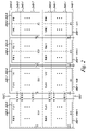
- FIG. 4 illustrates another previous approach to memory block management.
- the example shown in FIG. 4 includes a number of memory arrays 402 - 0 , 402 - 1 , 402 - 2 , . . . , 402 -(K- 1 ).
- the memory arrays 402 - 0 , 402 - 1 , 402 - 2 , . . . , 402 -(K- 1 ) can be analogous to memory arrays such as array 102 shown in FIG. 1 and memory arrays 202 - 0 and 202 - 1 shown in FIG. 2 .
- 402 -(K- 1 ) can be a portion of a memory unit such as memory unit 925 described below in connection with FIG. 9 .
- one or more of the arrays 402 - 0 , 402 - 1 , 402 - 2 , . . . , 402 -(K- 1 ) can be from different memory devices, e.g., from different flash memory dies or chips.
- the arrays 402 - 0 , 402 - 1 , 402 - 2 , . . . , 402 -(K- 1 ) each include a number of physical blocks of memory cells, with the blocks of each array organized into planes, e.g., PLANE 0 and PLANE 1 as shown in this example.
- the physical blocks within each of the arrays 402 - 0 , 402 - 1 , 402 - 2 , . . . , 402 -(K- 1 ) can have a block position 422 associated therewith.
- the block position 422 of a block can indicate the block's physical location within its respective plane.
- each memory array 402 - 0 , 402 - 1 , 402 - 2 , . . . , 402 -(K- 1 ) includes two physical blocks (one per plane) at the same block position 422 .
- each of the arrays 402 - 0 , 402 - 1 , 402 - 2 , . . . , 402 -(K- 1 ) include two blocks at block position BP 0 , two blocks at block position BP 1 , etc.
- the planes (Plane 0 and Plane 1 ) from each of the arrays 402 - 0 through 402 -(K- 1 ) are collectively organized as a single Group of planes.
- FIG. 4 illustrates a block status associated with the physical memory blocks within the arrays 402 - 0 , 402 - 1 , 402 - 2 , . . . , 402 -(K- 1 ).
- the arrays 402 - 0 , 402 - 1 , 402 - 2 , . . . , 402 -(K- 1 ) include a number of bad blocks 447 (labeled as BAD BLK) as well as a number of forced bad blocks 449 (labeled as FBB).
- the example shown in FIG. 4 also illustrates a number of Super Blocks, e.g., 445 - 1 (SUPER BLOCK 1 ) and 445 - 2 (SUPER BLOCK 2 ).
- the Super Blocks can be collections of physical blocks from each of at least two different planes with no more than one physical block from a particular plane.
- the Super Blocks, e.g., 445 - 1 and 445 - 2 are each a collection of “N” physical blocks across the multiple arrays 402 - 0 , 402 - 1 , 402 - 2 , . . . , 402 -(K- 1 ).
- each physical block within a Super Block has a particular block number 424 , e.g., the “N” physical blocks within the Super Blocks are numbered Block 0 through Block (N- 1 ) across the arrays 402 - 0 , 402 - 1 , 402 - 2 , . . . , 402 -(K- 1 ).
- each Super Block e.g., 445 - 1 and 445 - 2
- N total physical blocks e.g., two physical blocks (one from each of PLANE 0 and PLANE 1 ) from each of the memory arrays 402 - 0 , 402 - 1 , 402 - 2 , . . . , 402 -(K- 1 ).
- the physical blocks are assigned to Super Blocks such that the physical blocks corresponding to a particular Super Block are each at the same block position 422 . That is, each physical block, e.g., Block 0 through Block (N- 1 ), of a particular Super Block, is at the same block position 422 within its plane.
- Super Block 445 - 1 includes all the physical blocks at block position BP 0 across the arrays 402 - 0 through 402 -(K- 1 ).
- Super Block 445 - 2 includes all the physical blocks at block position BP 5 across the arrays 402 - 0 through 402 -(K- 1 ).
- the physical blocks assigned to the Super Blocks in the example shown in FIG. 4 each share the same block position 422 , if one of the arrays 402 - 0 through 402 -(K- 1 ) includes a bad block 447 at a particular block position, such as block position BP 2 , then all of the other physical blocks in a prospective Super Block including bad block 447 will be forced as bad blocks 449 . Accordingly, the physical blocks at that particular position 422 will not be assigned to a Super Block. For example, since the physical block located at BP 2 of Plane 1 within array 402 - 0 includes a bad block 447 , no physical blocks at the BP 2 position will be assigned to a Super Block.
- each of the physical blocks at block positions BP 3 , BP 7 , BP 8 , and BP 11 are also not assigned to a Super Block (since there is a bad block 447 at each of those block positions). As such, otherwise non-defective physical blocks associated at those block positions are treated as defective for purposes of Super Block assignment.
- Assigning N physical blocks to a Super Block, e.g., 445 - 1 or 445 - 2 , in the manner illustrated in FIG. 4 can reduce the amount of available Super Blocks within the Group of planes associated with arrays 402 - 0 , 402 - 1 , 402 - 2 , . . . , 402 -(K- 1 ). For instance, in the example illustrated in FIG. 4 , physical blocks at five of the twelve block positions, e g., BP 2 , BP 3 , BP 7 , BP 8 , and BP 11 , are unavailable for assignment of a Super Block thereto.
- each Super Block e.g., 445 - 1 and 445 - 2
- the size of the LUT can be smaller than the example described in connection with FIG. 3
- the time to reconstruct a Super Block is reduced since a single table search can result in the appropriate physical location of the physical blocks corresponding to a particular Super Block.
- Assigning N physical blocks to a Super Block, e.g., 445 - 1 or 445 - 2 , in the manner illustrated in FIG. 4 can reduce the LUT storage space and the Super Block reconstruction time by a factor of N/2 as compared to the example described in connection with FIG. 3 .
- FIG. 5 illustrates memory block management in accordance with one or more embodiments of the present disclosure.
- the embodiment shown in FIG. 5 includes a number of memory arrays 502 - 0 , 502 - 1 , 502 - 2 , . . . , 502 -(K- 1 ).
- the memory arrays 502 - 0 , 502 - 1 , 502 - 2 , . . . , 502 -(K- 1 ) can be analogous to memory arrays such as array 102 shown in FIG. 1 and memory arrays 202 - 0 and 202 - 1 shown in FIG. 2 .
- 502 -(K- 1 ) can be a portion of a memory unit such as memory unit 925 described below in connection with FIG. 9 .
- one or more of the arrays 502 - 0 , 502 - 1 , 502 - 2 , . . . , 502 -(K- 1 ) can be from different memory devices, e.g., from different flash memory dies or chips.
- the arrays 502 - 0 , 502 - 1 , 502 - 2 , . . . , 502 -(K- 1 ) each include a number of physical blocks of memory cells, with the blocks of each array organized into planes, e.g., PLANE 0 and PLANE 1 as shown.
- the physical blocks within each of the arrays 502 - 0 , 502 - 1 , 502 - 2 , . . . , 502 -(K- 1 ) can have a block position 522 associated therewith.
- the block position 522 of a block can indicate the block's physical location within its respective plane.
- each memory array 502 - 0 , 502 - 1 , 502 - 2 , . . . , 502 -(K- 1 ) includes two physical blocks (one per plane) at the same block position 522 .
- each of the arrays 502 - 0 , 502 - 1 , 502 - 2 , . . . , 502 -(K- 1 ) include two blocks at block position number BP 0 , two blocks at block position BP 1 , etc.
- the planes (Plane 0 and Plane 1 ) from each of the arrays 502 - 0 through 502 -(K- 1 ) are collectively organized as a single Group of planes.
- the embodiment shown in FIG. 5 includes a block status associated with the physical memory blocks within the arrays 502 - 0 , 502 - 1 , 502 - 2 , . . . , 502 -(K- 1 ).
- the arrays 502 - 0 , 502 - 1 , 502 - 2 , . . . , 502 -(K- 1 ) include a number of bad blocks 547 (labeled as BAD BLK).
- empty blocks represent non-defective physical blocks
- shaded blocks represent physical blocks assigned to a particular Super Block.
- a Super Block can be a collection of physical blocks from each of at least two different planes and having no more than one physical block from a particular one of those planes.
- the Super Blocks are each a collection of “N” physical blocks across the multiple arrays 502 - 0 , 502 - 1 , 502 - 2 , . . . , 502 -(K- 1 ).
- each physical block within a Super Block has a particular block number 524 , e.g., the “N” physical blocks within the Super Blocks are numbered Block 0 through Block (N- 1 ) across the arrays 502 - 0 , 502 - 1 , 502 - 2 , . . .
- each Super Block e.g., 545 - 1 , 545 - 2 A, and 545 - 2 B, is a collection of N total physical blocks, e.g., two physical blocks (one from each of PLANE 0 and PLANE 1 ) from each of the memory arrays 502 - 0 , 502 - 1 , 502 - 2 , . . . , 502 -(K- 1 ).
- each of the Super Blocks includes each physical block at the same particular block position 522 of at least two different planes that has not been determined to be defective (hereinafter a “non-defective block”) and a replacement physical block for each bad physical block at the same particular block position as the non-defective physical blocks, with the replacement physical block being at a different block position than the non-defective physical blocks.
- non-defective block a replacement physical block for each bad physical block at the same particular block position as the non-defective physical blocks, with the replacement physical block being at a different block position than the non-defective physical blocks.
- each of the non-defective blocks at that particular block position 522 are assigned to a particular Super Block, e.g., 545 - 2 A, in which one or more replacement physical blocks are assigned to the particular Super Block, e.g., 545 - 2 A, as replacements for the one or more bad physical blocks 547 at the particular block position.
- a particular Super Block e.g., 545 - 2 A
- replacement physical blocks are assigned to the particular Super Block, e.g., 545 - 2 A, as replacements for the one or more bad physical blocks 547 at the particular block position.
- the replacement physical block is from the same plane as the bad physical block 547 which it is replacing in the particular Super Block, e.g., 545 - 2 A and 545 - 2 B.
- control circuitry coupled to the memory arrays e.g., 502 - 0 through 502 -(K- 1 ), is configured to map the bad physical blocks 547 at the particular block position 522 to the replacement physical blocks at the different block position.
- the embodiment illustrated in FIG. 5 includes two types of Super Blocks.
- the physical blocks at a particular block position 522 that has no bad blocks 547 associated therewith are assigned to a first type of Super Block, e.g., Super Block 545 - 1 .
- all of the physical blocks at block position BP 0 are assigned to Super Block 545 - 1 .
- the non-defective physical blocks at a particular block position 522 which has one or more bad blocks 547 associated therewith, are assigned to a second type of Super Block that also includes replacement physical blocks assigned thereto, e.g., Super Blocks 545 - 2 A or 545 - 2 B.
- a second type of Super Block that also includes replacement physical blocks assigned thereto, e.g., Super Blocks 545 - 2 A or 545 - 2 B.
- the physical block located at block position BP 2 within Plane 0 of array 502 - 0 is a bad block 547 .
- a replacement block e.g., the physical block located at block position BP 12 within Plane 0 of array 502 - 0 , is assigned to Super Block 545 - 2 A along with the non-defective blocks at block position BP 2 . That is block number Block 0 of Super Block 545 - 2 A is a replacement block.
- the physical blocks at block position BP 3 include two bad blocks 547 , e.g., the block within Plane 0 of array 502 - 1 and the block within Plane 1 of array 502 -(K- 1 ).
- block number Block 2 and block number Block (N- 1 ) of Super Block 545 - 2 B are replacement blocks, e.g., the physical block located at block position BP 12 within Plane 0 of array 502 - 1 and the physical block located at block position BP 12 within Plane 1 of array 502 -(K- 1 ) are assigned to Super Block 545 - 2 B as replacement blocks for the respective bad blocks 547 at block position BP 3 .
- the physical blocks are assigned to Super Blocks in such a way that the physical blocks assigned to a first type, e.g., 545 - 1 , of Super Block are each at the same block position 522 . That is, each physical block, e.g., Block 0 through Block (N- 1 ), of a particular first type of Super Block are at the same block position 522 .
- physical blocks are also assigned to Super Blocks in such a way that at least one of the physical blocks assigned to a second type, e.g., 545 - 2 A or 545 - 2 B, of Super Block are at a different block position 522 . That is, the replacement physical block(s) assigned to a particular second type of Super Block are at a different block position 522 than the non-defective blocks assigned to that particular Super Block.
- a memory controller e.g., memory controller 920 described in connection with FIG. 9
- the arrays 502 - 0 through 502 -(K- 1 ) include a portion 533 assigned for remapping.
- each of the physical blocks at block positions BP 12 , BP 13 , and BP 14 are assigned for replacing a bad block 547 in their respective plane and can be assigned to a particular Super Block of type 2 , e.g., 545 - 2 A or 545 - 2 B.
- the replacement physical blocks can be used for remapping bad blocks to non-defective physical blocks.
- the control circuitry can be configured to assign a predetermined number of physical blocks within each plane to be used to replace bad physical blocks 547 within the plane.
- the particular number of physical blocks assigned to be used to replace bad physical blocks is based, at least partially, on an uppermost expected number of defective blocks per plane. For instance, a manufacturer of the memory arrays 502 - 0 through 502 -(K- 1 ) may indicate that not more than about 2% to about 4% of the physical blocks per plane will be defective over the life of the arrays. For example, not more than about 2% to about 4% of the physical blocks in the arrays 502 - 0 through 502 -(K- 1 ) will be bad blocks 547 . In various embodiments, the particular number of physical blocks assigned for remapping 533 does not exceed the uppermost expected number of defective blocks per plane.
- the portion 533 assigned for remapping may be about 2% to about 4% of the total number of physical blocks per plane.
- Embodiments of the present disclosure are not limited to a particular expected percentage of, or number of, defective blocks per plane.
- the number of expected defective blocks per plane can include “original” defective blocks (e.g., blocks that are defective at the time of manufacture and/or by preliminary testing) as well as blocks which are functionally good at the time of manufacture and preliminary testing, but become defective during the life of a memory device (e.g., a flash memory device). Blocks which become defective after preliminary testing (e.g., during the life of the device) can be referred to as “grown” defective blocks.
- the number of expected defective blocks associated with a particular plane can include the original defective blocks as well as the grown defective blocks from each plane.
- a replacement block from the portion 533 for remapping can also be used to replace blocks that are determined to be defective during use of the memory device (e.g., to replace grown defective blocks).
- the Super Block which contained the grown defective block can remain the same; however, the grown defective physical block will be dynamically replaced with a physical block from the portion 533 for remapping.
- Assigning N physical blocks to a Super Block, e.g., 545 - 1 , 545 - 2 A or 545 - 2 B, in the manner illustrated in FIG. 5 can provide improved block management efficiency as compared to the previous approaches described in connection with FIGS. 3 and 4 .
- a single LBA to PBA mapping entry in a LUT can be used to locate the physical blocks assigned to a Super Block of type 1 , e.g., 545 - 1 , since the physical blocks corresponding to a Super Block of type 1 are at a common block position 522 .
- a single LBA to PBA mapping entry in a LUT can be used to locate the physical blocks assigned to a Super Block of type 1 , e.g., 545 - 1 , since the physical blocks corresponding to a Super Block of type 1 are at a common block position 522 .
- physical blocks that share a block position n with one or more bad blocks 547 can be assigned to a Super Block of type 2 , e.g., 545 - 2 A or 545 - 2 B, which can reduce the inefficiency associated with forced bad blocks.
- a separate LUT can be used to map LBAs to PBAs for Super Blocks of type 2 .
- the storage space used for storing the LUT used to map LBAs to PBAs for Super Blocks of type 2 can be small as compared to the LUT used to map LBAs to PBAs for Super Blocks of type 1 . For instance, since there can be a relatively small number, e.g., 2-4%, of bad blocks 547 , the number of Super Blocks of type 2 can be small as compared to the number of Super Blocks of type 1 .
- FIG. 6 illustrates memory block management in accordance with one or more embodiments of the present disclosure.
- the embodiment shown in FIG. 6 includes a number of memory arrays 602 - 0 , 602 - 1 , 602 - 2 , . . . , 602 -(K- 1 ).
- the memory arrays 602 - 0 , 602 - 1 , 602 - 2 , . . . , 602 -(K- 1 ) can be analogous to memory arrays such as array 102 shown in FIG. 1 and memory arrays 202 - 0 and 202 - 1 shown in FIG. 2 .
- 602 -(K- 1 ) can be a portion of a memory unit such as memory unit 925 described below in connection with FIG. 9 .
- one or more of the arrays 602 - 0 , 602 - 1 , 602 - 2 , . . . , 602 -(K- 1 ) can be from different memory devices, e.g., from different flash memory dies or chips.
- the arrays 602 - 0 , 602 - 1 , 602 - 2 , . . . , 602 -(K- 1 ) each include a number of physical blocks of memory cells, with the blocks of each array organized into planes, e.g., PLANE 0 and PLANE 1 as shown.
- the physical blocks within each plane of the arrays 602 - 0 , 602 - 1 , 602 - 2 , . . . , 602 -(K- 1 ) are at a different block position 622 associated therewith.
- the block position 622 of a block can indicate the block's physical location within its respective plane.
- each memory array 602 - 0 , 602 - 1 , 602 - 2 , . . . , 602 -(K- 1 ) includes two physical blocks (one per plane) at the same block position 622 .
- each of the arrays 602 - 0 , 602 - 1 , 602 - 2 , . . . , 602 -(K- 1 ) include two blocks at block position BP 0 , two blocks having position number BP 1 , etc.
- the planes (Plane 0 and Plane 1 ) from each of the arrays 602 - 0 through 602 -(K- 1 ) are collectively organized as a single Group of planes (e.g., Group 240 - 0 or 240 - 1 shown in FIG. 2 ).
- the embodiment shown in FIG. 6 includes a block status associated with the physical memory blocks within the arrays 602 - 0 , 602 - 1 , 602 - 2 , . . . , 602 -(K- 1 ).
- the arrays 602 - 0 , 602 - 1 , 602 - 2 , . . . , 602 -(K- 1 ) include a number of bad blocks 647 (labeled as BAD BLK) as well as a number of forced bad blocks 649 (labeled as FBB).
- BAD BLK bad blocks
- FBB forced bad blocks
- a Super Block can be a collection of physical blocks from each of at least two different planes and have no more than one physical block from a particular one of the planes.
- non-defective physical blocks at a common block position 622 within a particular array as a bad block 647 are forced bad blocks 649 .
- the physical block of Plane 1 at block position BP 2 is a forced bad block 649 since it shares block position BP 2 with bad block 647 of Plane 0 .
- the embodiment illustrated in FIG. 6 includes two types of Super Blocks, e.g., type 1 645 - 1 and type 2 645 - 2 .
- Each Super Block is a collection of “N” physical blocks across the multiple arrays 602 - 0 , 602 - 1 , 602 - 2 , . . . , 602 -(K- 1 ).
- FIG. 6 illustrates two types of Super Blocks, e.g., type 1 645 - 1 and type 2 645 - 2 .
- Each Super Block is a collection of “N” physical blocks across the multiple arrays 602 - 0 , 602 - 1 , 602 - 2 , . . . , 602 -(K- 1 ).
- each physical block within a Super Block has a particular block number 624 , e.g., the “N” physical blocks within the Super Blocks are numbered Block 0 through Block (N- 1 ) across the arrays 602 - 0 , 602 - 1 , 602 - 2 , . . . , 602 -(K- 1 ).
- the “N” physical blocks within the Super Blocks are numbered Block 0 through Block (N- 1 ) across the arrays 602 - 0 , 602 - 1 , 602 - 2 , . . . , 602 -(K- 1 ).
- each Super Block e.g., 645 - 1 and 645 - 2
- N total physical blocks e.g., two physical blocks (one from each of PLANE 0 and PLANE 1 ) from each of the memory arrays 602 - 0 , 602 - 1 , 602 - 2 , . . . , 602 -(K- 1 ).
- each of the Super Blocks of the first type e.g., 645 - 1 includes all of the non-defective physical blocks at a same particular block position 622 of at least two different memory arrays. That is, there are no bad blocks 647 or forced bad blocks 649 at the block position 622 of the physical blocks assigned to a Super Block of type 1 , e.g., 645 - 1 .
- non-defective physical blocks at the same block position 622 as a bad block 647 are available for assignment to a Super Block of type 2 , e.g., 645 - 2 .
- the non-defective physical blocks located at block position BP 3 within Plane 0 and Plane 1 of array 602 - 0 are assigned to Super Block 645 - 2 , e.g., as Block 0 and Block 1 of Super Block 645 - 2 .
- the non-defective physical blocks located at block position BP 7 within Plane 0 and Plane 1 of array 602 - 1 are also assigned to Super Block 645 - 2 , e.g., as Block 2 and Block 3 of Super Block 645 - 2 .
- non-defective physical blocks located at block position BP 8 within Plane 0 and Plane 1 of array 602 - 2 are assigned to Super Block 645 - 2 , e.g., as Block 4 and Block 5 of Super Block 645 - 2 .
- the non-defective physical blocks located at block position BP 7 within Plane 0 and Plane 1 of array 602 -(K- 1 ) (where a bad block 647 is also located at block position BP 7 within Plane 1 of array 602 - 0 ) is assigned to Super Block 645 - 2 , e.g., as Block (N- 2 ) and Block (N- 1 ) of Super Block 645 - 2 .
- a memory controller e.g., memory controller 920 described in FIG. 9
- Assigning N physical blocks to a Super Block, e.g., 645 - 1 or 645 - 2 , in the manner illustrated in FIG. 6 can provide improved block management efficiency as compared to the previous approaches described in connection with FIGS. 3 and 4 .
- a single LBA to PBA mapping entry in a LUT can be used to locate the physical blocks assigned to a Super Block of type 1 , e.g., 645 - 1 , since the physical blocks corresponding to a Super Block of type 1 share a common block position 622 .
- non-defective physical blocks that share a common block position with one or more bad blocks 647 are available to be assigned to a Super Block of type 2 , e.g., 645 - 2 .
- a separate LUT can be used to map LBAs to PBAs for Super Blocks of type 2 .
- the storage space used for storing the LUT used to map LBAs to PBAs for Super Blocks of type 2 can be small as compared to the LUT used to map LBAs to PBAs for Super Blocks of type 1 . For instance, since there can be a relatively small number, e.g., 2-4%, of bad blocks 647 , the number of Super Blocks of type 2 can be small as compared to the number of Super Blocks of type 1 .
- FIG. 7 illustrates memory block management in accordance with one or more embodiments of the present disclosure.
- the embodiment shown in FIG. 7 includes a number of memory arrays 702 - 0 , 702 - 1 , 702 - 2 , . . . , 702 -(K- 1 ).
- the memory arrays 702 - 0 , 702 - 1 , 702 - 2 , . . . , 702 -(K- 1 ) can be analogous to memory arrays such as array 102 shown in FIG. 1 and memory arrays 202 - 0 and 202 - 1 shown in FIG. 2 .
- 702 -(K- 1 ) can be a portion of a memory unit such as memory unit 925 described below in connection with FIG. 9 .
- one or more of the arrays 702 - 0 , 702 - 1 , 702 - 2 , . . . , 702 -(K- 1 ) can be from different memory devices, e.g., from different flash memory dies or chips.
- the arrays 702 - 0 , 702 - 1 , 702 - 2 , . . . , 702 -(K- 1 ) each include a number of physical blocks of memory cells, with the blocks of each array organized into planes, e.g., PLANE 0 and PLANE 1 as shown.
- the physical blocks within each of the arrays 702 - 0 , 702 - 1 , 702 - 2 , . . . , 702 -(K- 1 ) can have a block position 722 associated therewith. In this example, there are fifteen block positions: BP 0 to BP 14 .
- the block position 722 of a block can indicate the block's physical location within its respective plane.
- each memory array 702 - 0 , 702 - 1 , 702 - 2 , . . . , 702 -(K- 1 ) includes two physical blocks (one per plane) at the same block position 722 .
- each of the arrays 702 - 0 , 702 - 1 , 702 - 2 , . . . , 702 -(K- 1 ) include two blocks at block position BP 0 , two blocks at block position BP 1 , etc.
- the planes (Plane 0 and Plane 1 ) from each of the arrays 702 - 0 through 702 -(K- 1 ) are organized as two respective Groups of planes.
- the embodiment shown in FIG. 7 includes a block status associated with the physical memory blocks within the arrays 702 - 0 , 702 - 1 , 702 - 2 , . . . , 702 -(K- 1 ).
- the arrays 702 - 0 , 702 - 1 , 702 - 2 , . . . , 702 -(K- 1 ) include a number of bad blocks 747 (labeled as BAD BLK).
- empty blocks represent non-defective physical blocks
- shaded blocks represent physical blocks assigned to a particular Super Block.
- a Super Block can be a collection of physical blocks from each of at least two different planes and have no more than one physical block from a particular one of the planes.
- each physical block within a Super Block has a particular block number 724 , e.g., the “N/2” physical blocks within the Super Blocks are either the even numbered or odd numbered of Block 0 through Block (N- 1 ) across the arrays 702 - 0 , 702 - 1 , 702 - 2 , . . . , 702 -(K- 1 ).
- each Super Block e.g., 745 - 1 A, 745 - 1 B, and 745 - 1 C, 745 - 2 A, 745 - 2 B, and 745 - 2 C
- N/2 total physical blocks e.g., one physical block from either PLANE 0 or PLANE 1 from each of the memory arrays 702 - 0 , 702 - 1 , 702 - 2 , . . . , 702 -(K- 1 ).
- a Super Block of type 1 includes physical blocks located at block position BP 0 within Plane 0 of each of the arrays 702 - 0 through 702 -(K- 1 ).
- Another Super Block of type 1 e.g., 745 - 1 B, includes physical blocks located at block position BP 0 within Plane 1 of each of the arrays 702 - 0 through 702 -(K- 1 ).
- Still another Super Block of type 1 e.g., 745 - 1 C, includes physical blocks located at block position BP 2 within Plane 1 of each of the arrays 702 - 0 through 702 -(K- 1 ).
- each of the non-defective blocks at that particular block position 722 are assigned to a particular Super Block, e.g., 745 - 2 A, in which one or more replacement physical blocks are assigned to the particular Super Block, e.g., 745 - 2 A, as replacements for the one or more bad physical blocks 747 at the particular block position.
- a particular Super Block e.g., 745 - 2 A
- replacement physical blocks are assigned to the particular Super Block, e.g., 745 - 2 A, as replacements for the one or more bad physical blocks 747 at the particular block position.
- the replacement physical block is from the same plane as the bad physical block 747 which it is replacing in the particular Super Block, e.g., 745 - 2 A, 745 - 2 B, or 745 - 2 C.
- control circuitry coupled to the memory arrays e.g., 702 - 0 through 702 -(K- 1 ) is configured to map the bad physical blocks 747 at the particular block position 722 to the replacement physical blocks at the different block position.
- the embodiment illustrated in FIG. 7 includes two types of Super Blocks: 745 - 1 and 745 - 2 .
- non-defective physical blocks that share a particular block position 722 with one or more bad blocks 747 are assigned to a second type of Super Block that also includes a replacement physical block assigned thereto, e.g., Super Blocks 745 - 2 A, 745 - 2 B, or 745 - 2 C.
- a replacement physical block assigned thereto e.g., Super Blocks 745 - 2 A, 745 - 2 B, or 745 - 2 C.
- the physical block located at block position BP 2 within Plane 0 of array 702 - 0 is a bad block 747 .
- a replacement block e.g., the physical block located at block position BP 12 within Plane 0 of array 702 - 0
- Super Block 745 - 2 A is assigned to Super Block 745 - 2 A along with the non-defective blocks at the block position BP 2 within Plane 0 of arrays 702 - 1 through 702 -(K- 1 ). That is block number Block 0 of Super Block 745 - 2 A is a replacement block.
- the physical blocks at block position BP 3 include two bad blocks 747 , e.g., the block within Plane 0 of array 702 - 1 and the block within Plane 1 of array 702 -(K- 1 ).
- block number Block 2 of Super Block 745 - 2 B and block number Block (N- 1 ) of Super Block 745 - 2 C are replacement blocks, e.g., the physical block located at block position BP 12 within Plane 0 of array 702 - 1 and the physical block located at block position BP 12 within Plane 1 of array 702 -(K- 1 ) are assigned to Super Blocks 745 - 2 B and 745 - 2 C, respectively, as replacement blocks for the respective bad blocks 747 at block position BP 3 .
- physical blocks are assigned to Super Blocks of the first type, e.g., 745 - 1 A, 745 - 1 B, and 745 - 1 C, such that the physical blocks corresponding to a particular Super Block are each at the same respective block position 722 . That is, each of the N/2 physical blocks of a particular Super Block shares the same block position 722 .
- Physical blocks are assigned to Super Blocks of the second type, e.g., 745 - 2 A, 745 - 2 B, and 745 - 2 C, such that at least one of the N/2 physical blocks of a particular Super Block of the second type is at a different block position 722 . That is, the replacement physical block(s) assigned to the particular Super Block of the second type is at a different block position 722 than the non-defective blocks assigned to the particular Super Block of the second type.
- a memory controller e.g., memory controller 920 described in connection with FIG. 9
- the arrays 702 - 0 through 702 -(K- 1 ) include a portion 733 assigned for remapping.
- each of the physical blocks at block positions BP 12 , BP 13 , and BP 14 are assigned for replacing a respective bad block 747 and can be assigned to a particular Super Block of type 2 , e.g., 745 - 2 A, 745 - 2 B, or 745 - 2 C.
- Assigning N/2 physical blocks to a Super Block e.g., 745 - 1 A, 745 - 1 B, 745 - 1 C, 745 - 2 A, 745 - 2 B, or 745 - 2 C, in the manner illustrated in FIG. 7 , can provide improved block management efficiency as compared to the previous approaches described in connection with FIGS. 3 and 4 .
- a Super Block e.g., 745 - 1 A, 745 - 1 B, 745 - 1 C, 745 - 2 A, 745 - 2 B, or 745 - 2 C
- a single LBA to PBA mapping entry in a LUT can be used to locate the physical blocks assigned to a Super Block of type 1 , e.g., 745 - 1 A, 745 - 1 B, or 745 - 1 C, since the physical blocks corresponding to a Super Block of type 1 share a common block position 722 .
- non-defective physical blocks that share a common block position with one or more bad blocks 747 can be assigned to a Super Block of type 2 , e.g., 745 - 2 A, 745 - 2 B, or 745 - 2 C, which can reduce the inefficiency associated with forced bad blocks.
- a separate LUT can be used to map LBAs to PBAs for Super Blocks of type 2 .
- the storage space used for storing the LUT used to map LBAs to PBAs for Super Blocks of type 2 can be small as compared to the LUT used to map LBAs to PBAs for Super Blocks of type 1 . For instance, since there can be a relatively small number, e.g., 2-4%, of bad blocks 747 , the number of Super Blocks of type 2 can be small as compared to the number of Super Blocks of type 1 .
- FIGS. 8A , 8 B, and 8 C illustrate tables having mapping information that can be used in accordance with one or more embodiments of the present disclosure.
- LBAs can be received by a memory controller in association with a particular operation, e.g., program, read, erase, etc.
- a look up table (LUT) includes logical block address (LBA) to physical block address (PBA) mappings that can provide the physical locations of the physical blocks assigned to particular Super Blocks based on the received LBA.
- LBA logical block address
- PBA physical block address
- FIG. 8A illustrates an example LUT 842 that includes LBA to PBA mappings corresponding to Super Blocks of different types, e.g., type 1 and type 2 , as described herein in connection with FIGS. 5 , 6 , and 7 .
- the indicator “P” represents the total number of physical blocks per plane within the multiple memory arrays associated with Super Blocks.
- the indicator “M” represents an uppermost number of defective blocks per plane within the multiple memory arrays. As described above, the number “M” can be provided by a manufacturer, for instance, as an expected maximum number of defective blocks per plane over the life of a particular memory array.
- P-M represents the total number of usable physical blocks per plane and, as such, there can be “P-M” Super Blocks. Of the “P-M” Super Blocks, most will be Super Blocks of type 1 , e.g., 545 - 1 or 645 - 1 described in connection with FIGS. 5 and 6 , respectively, since there is a relatively small amount, e.g., 2%-4%, of bad blocks per plane.
- the table 842 includes “P-M” entries corresponding to a number of super LBAs (labeled SUPER LBA 0 through SUPER LBA (P-M- 1 ) as shown).
- table 842 is a single entry table, e.g., each super LBA corresponds to a single entry.
- the entries 850 - 0 , 850 - 1 , 850 - 2 , and 850 - 3 represent entries corresponding to Super Blocks of type 1 . That is, since each of the physical blocks assigned to a Super Block of type 1 share a common block position, e.g., 522 / 622 shown in FIG. 5 / 6 , a single entry can be used to determine the physical location of all of the physical blocks assigned to the particular Super Block of type 1 .
- the entry 852 represents an entry corresponding to a Super Block of type 2 , e.g., a Super Block having one or more physical blocks assigned thereto that have different block positions, as described in connection with FIGS. 5 , 6 , and 7 . Since the physical blocks assigned to a type 2 Super Block can have various block positions across the multiple arrays, unlike the entries 850 - 1 , 850 - 2 , 850 - 2 , and 850 - 3 , the entry 852 does not include direct LBA to PBA mapping. Instead, the entry 852 includes an indication of a different table, e.g., table 860 , which includes LBA to PBA mappings for Super Blocks of type 2 .
- table 860 which includes LBA to PBA mappings for Super Blocks of type 2 .
- a single entry table e.g., 842
- a single entry table can first be searched based on the particular super LBA. If it is determined that the entry within table 842 that corresponds to the particular LBA is an entry corresponding to a PBA associated with a Super Block of type 2 , e.g., 852 , then a table such as table 860 can be searched to determine the appropriate mapping information indicating the physical locations of the physical blocks assigned to the particular type 2 Super Block. That is, the table 860 can include a PBA for each physical block in the collection of physical blocks corresponding to the particular type 2 Super Block. Examples of type 2 tables, such as table 860 , which contain LBA to PBA mappings for Super Blocks of type 2 , are illustrated in FIGS. 8B and 8C .
- FIGS. 8B and SC illustrate example LUTs 844 - 1 and 844 - 2 that each include LBA to PBA mappings corresponding to Super Blocks of type 2 .
- Tables 844 - 1 and 844 - 2 can be tables such as table 860 , which are searched in response to an indication within a table such as table 842 shown in FIG. 8A .
- LUT 844 - 1 includes (M ⁇ N) entries, where “M” represents an uppermost number of expected defective blocks per plane within the multiple memory arrays, and “N” represents the number of physical blocks per Super Block.
- each of the entries 862 - 0 , 862 - 1 , . . . , 862 -(N- 1 ) includes LBA to PBA mapping information corresponding to a particular physical block assigned to a particular type 2 Super Block, e.g., 545 - 2 A or 545 - 2 B described in connection with the embodiment of FIG. 5 .
- LUT 844 - 2 includes [M ⁇ (N/2)] entries, where “M” represents an uppermost number of expected defective blocks per plane within the multiple memory arrays, and “N” represents the number of physical blocks per Super Block.
- each of the entries 864 - 0 , 864 - 1 , . . . , 864 -[(N- 1 )/2] includes LBA to PBA mapping information corresponding to a particular pair of physical blocks (from Plane 0 and Plane 1 of a particular array) assigned to a particular type 2 Super Block, e.g., 645 - 2 described in connection with the embodiment of FIG. 6 .
- some memory systems are configured such that operations are performed on the physical blocks within both planes of a particular array at the same time.
- a physical block that shares a common block position with a bad block within the same array may be forced as unusable by the system.
- physical blocks which share a block position 622 with and are in the same array as a bad block 647 become forced bad blocks 649 .
- the table 844 - 2 of FIG. 8C can have half as many entries as table 844 - 1 of FIG. 8B when the memory system, e.g., 900 shown in FIG. 9 , is configured to perform operations on the physical blocks within both planes of the multiple memory arrays at once.
- FIG. 9 is a functional block diagram of an electronic memory system 900 in accordance with one or more embodiments of the present disclosure.
- the system 900 is a solid state drive (SSD), e.g., a flash SSD. That is, the embodiment of FIG. 9 can illustrate the components and architecture of one embodiment of a solid state drive 900 .
- the system 900 includes a controller 920 , a host interface 924 , an array interface 926 , and solid state memory unit 925 .
- the memory unit 925 includes a number of memory devices 930 - 0 , 930 - 1 , . . . , 930 -D.
- the memory devices can be non-volatile memory devices such as flash memories, e.g., NAND flash or NOR flash devices, among others.
- the memory devices 930 - 0 , 930 - 1 , . . . , 930 -D can be memory devices such as memory devices 230 - 0 , 230 - 1 , 230 - 2 , and 230 - 3 described in connection with FIG. 2 .
- FIG. 9 the memory unit 925 includes a number of memory devices 930 - 0 , 930 - 1 , . . . , 930 -D.
- the memory devices can be non-volatile memory devices such as flash memories, e.g., NAND flash or NOR flash devices, among others.
- each of the memory devices 930 - 0 , 930 - 1 , . . . , 930 -D includes a number of memory arrays 902 - 0 , 902 - 1 , 902 - 3 , . . . , 902 -(K- 1 ).
- the memory arrays 902 - 0 , 902 - 1 , 902 - 3 , . . . , 902 -(K- 1 ) can be arrays such as the memory arrays described in connection with FIGS. 5 , 6 , and 7 .
- each of the memory arrays 902 - 0 , 902 - 1 , 902 - 3 , . . . , 902 -(K- 1 ) can represent a single die, and each of the memory devices 930 - 0 , 930 - 1 , . . . , 930 -D can represent a memory chip having multiple dies per chip.
- the memory unit 925 can be organized into multiple Groups of planes across the memory arrays with each Group being a collection of at least two planes from different memory devices. As described above in connection with FIG. 2 , the Groups can have a number of Super Blocks associated therewith, with the Super Blocks being a collection of a physical block from each of the at least two planes of the Group. In various embodiments, the at least two planes of the Group can be located on at least two different memory arrays.
- the memory unit 925 can be coupled to the controller 920 via an array interface 926 .
- the array interface 926 can be used to communicate information between the memory unit 925 and the controller 920 .
- the controller 920 can be coupled to a memory access device, e.g., a processor of a host device (not shown), via host interface 924 .
- a host device can include a computing device such as a personal computer (PC), a laptop computer, a digital camera, or a cellular telephone, among various other computing devices.
- PC personal computer
- FIG. 9 when the memory unit 925 is used for data storage in a computing device, as illustrated in FIG.
- the host interface 924 can be a serial advanced technology attachment (SATA), among others, e.g., the controller 920 can be a SATA controller or a USB controller, among others. That is, embodiments are not limited to a particular type of controller 920 and/or host interface 924 .
- SATA serial advanced technology attachment
- the controller 920 includes control circuitry 922 .
- the control circuitry 922 can include a processor 923 , a space manager 927 , memory 929 , e.g., a RAM, among other control circuitry (not shown) for operation of memory system 900 .
- the controller 920 is used to write data to and read data from the memory unit 925 .
- the controller 920 can receive logical block addresses (LBAs) 931 from a host device via the host interface 924 .
- the control circuitry 922 can be configured to search one or more look up tables, such as tables 842 , 844 - 1 , and 844 - 2 , to determine the physical location of physical blocks assigned to particular Super Blocks.
- control circuitry 922 can be configured to selectively assign physical blocks to either Super Blocks of a first type or Super Blocks of a second type, with the Super Blocks being collections of physical blocks from each of at least two different planes.
- the at least two different planes can be from different memory arrays.
- the control circuitry 922 can be configured to assign physical blocks to particular Super Blocks as described, for example, in FIGS. 5 , 6 , and 7 .
- the present disclosure includes methods and devices for memory block management in a memory system. Embodiments of the present disclosure can improve the efficiency of memory block management as compared to previous approaches.
- One or more embodiments of the present disclosure include one or more memory devices having at least two planes of physical blocks organized into super blocks, with each super block including a physical block from each of the at least two planes.
- One or more embodiments include determining defective physical blocks within the planes.
- one or more embodiments include assigning the physical blocks at the particular block position to a super block, and if one or more of the physical blocks at a particular block position are determined to be defective, one or more embodiments include: assigning the physical blocks at the particular block position that were not determined to be defective to a super block; and assigning a respective replacement physical block to the super block for each of the one or more physical blocks at the particular block position that were determined to be defective.
- the respective replacement physical block is selected from a number of physical blocks within a respective one of the planes that includes the respective physical block that was determined to be defective.
- One or more embodiments of the present disclosure include determining defective physical blocks within a memory unit having multiple Groups of planes associated therewith, each Group including at least two planes of physical blocks organized into Super Blocks, with each Super Block including a physical block from each of the at least two planes.
- Embodiments can include assigning collections of blocks from each of the at least two planes of a respective Group to respective Super Blocks.
- a Super Block can include: a collection of all non-defective blocks having the same particular position number within each of the at least two planes of a respective Group; and a replacement block for each defective block having the same particular position number as the non-defective blocks.
- the replacement block can be selected from a group of blocks within each plane assigned to be used to replace defective blocks within the respective plane.
Abstract
Description
Claims (30)
Priority Applications (8)
| Application Number | Priority Date | Filing Date | Title |
|---|---|---|---|
| US12/397,396 US8095765B2 (en) | 2009-03-04 | 2009-03-04 | Memory block management |
| CN201080010244.8A CN102341792B (en) | 2009-03-04 | 2010-02-24 | Memory block management |
| EP10749034.4A EP2404240B1 (en) | 2009-03-04 | 2010-02-24 | Memory block management |
| PCT/US2010/000540 WO2010101609A2 (en) | 2009-03-04 | 2010-02-24 | Memory block management |
| JP2011552933A JP2012519900A (en) | 2009-03-04 | 2010-02-24 | Memory block management |
| KR1020117023034A KR101327693B1 (en) | 2009-03-04 | 2010-02-24 | Memory block management |
| TW099106313A TWI424315B (en) | 2009-03-04 | 2010-03-04 | Memory block management |
| US13/347,054 US8312245B2 (en) | 2009-03-04 | 2012-01-10 | Memory block management |
Applications Claiming Priority (1)
| Application Number | Priority Date | Filing Date | Title |
|---|---|---|---|
| US12/397,396 US8095765B2 (en) | 2009-03-04 | 2009-03-04 | Memory block management |
Related Child Applications (1)
| Application Number | Title | Priority Date | Filing Date |
|---|---|---|---|
| US13/347,054 Continuation US8312245B2 (en) | 2009-03-04 | 2012-01-10 | Memory block management |
Publications (2)
| Publication Number | Publication Date |
|---|---|
| US20100228940A1 US20100228940A1 (en) | 2010-09-09 |
| US8095765B2 true US8095765B2 (en) | 2012-01-10 |
Family
ID=42679255
Family Applications (2)
| Application Number | Title | Priority Date | Filing Date |
|---|---|---|---|
| US12/397,396 Active 2030-03-07 US8095765B2 (en) | 2009-03-04 | 2009-03-04 | Memory block management |
| US13/347,054 Active US8312245B2 (en) | 2009-03-04 | 2012-01-10 | Memory block management |
Family Applications After (1)
| Application Number | Title | Priority Date | Filing Date |
|---|---|---|---|
| US13/347,054 Active US8312245B2 (en) | 2009-03-04 | 2012-01-10 | Memory block management |
Country Status (7)
| Country | Link |
|---|---|
| US (2) | US8095765B2 (en) |
| EP (1) | EP2404240B1 (en) |
| JP (1) | JP2012519900A (en) |
| KR (1) | KR101327693B1 (en) |
| CN (1) | CN102341792B (en) |
| TW (1) | TWI424315B (en) |
| WO (1) | WO2010101609A2 (en) |
Cited By (44)
| Publication number | Priority date | Publication date | Assignee | Title |
|---|---|---|---|---|
| US20110035540A1 (en) * | 2009-08-10 | 2011-02-10 | Adtron, Inc. | Flash blade system architecture and method |
| US8312245B2 (en) * | 2009-03-04 | 2012-11-13 | Micron Technology, Inc. | Memory block management |
| US8909851B2 (en) | 2011-02-08 | 2014-12-09 | SMART Storage Systems, Inc. | Storage control system with change logging mechanism and method of operation thereof |
| US8935466B2 (en) | 2011-03-28 | 2015-01-13 | SMART Storage Systems, Inc. | Data storage system with non-volatile memory and method of operation thereof |
| US8949689B2 (en) | 2012-06-11 | 2015-02-03 | SMART Storage Systems, Inc. | Storage control system with data management mechanism and method of operation thereof |
| US9021319B2 (en) | 2011-09-02 | 2015-04-28 | SMART Storage Systems, Inc. | Non-volatile memory management system with load leveling and method of operation thereof |
| US9021231B2 (en) | 2011-09-02 | 2015-04-28 | SMART Storage Systems, Inc. | Storage control system with write amplification control mechanism and method of operation thereof |
| US9043780B2 (en) | 2013-03-27 | 2015-05-26 | SMART Storage Systems, Inc. | Electronic system with system modification control mechanism and method of operation thereof |
| US9063844B2 (en) | 2011-09-02 | 2015-06-23 | SMART Storage Systems, Inc. | Non-volatile memory management system with time measure mechanism and method of operation thereof |
| US9098399B2 (en) | 2011-08-31 | 2015-08-04 | SMART Storage Systems, Inc. | Electronic system with storage management mechanism and method of operation thereof |
| US9123445B2 (en) | 2013-01-22 | 2015-09-01 | SMART Storage Systems, Inc. | Storage control system with data management mechanism and method of operation thereof |
| KR20150103932A (en) * | 2014-03-04 | 2015-09-14 | 삼성전자주식회사 | Nonvolatile memory system and operation method thereof |
| US9146850B2 (en) | 2013-08-01 | 2015-09-29 | SMART Storage Systems, Inc. | Data storage system with dynamic read threshold mechanism and method of operation thereof |
| US9152555B2 (en) | 2013-11-15 | 2015-10-06 | Sandisk Enterprise IP LLC. | Data management with modular erase in a data storage system |
| US9170941B2 (en) | 2013-04-05 | 2015-10-27 | Sandisk Enterprises IP LLC | Data hardening in a storage system |
| US9183137B2 (en) | 2013-02-27 | 2015-11-10 | SMART Storage Systems, Inc. | Storage control system with data management mechanism and method of operation thereof |
| US9214965B2 (en) | 2013-02-20 | 2015-12-15 | Sandisk Enterprise Ip Llc | Method and system for improving data integrity in non-volatile storage |
| US9239781B2 (en) | 2012-02-07 | 2016-01-19 | SMART Storage Systems, Inc. | Storage control system with erase block mechanism and method of operation thereof |
| US9244519B1 (en) | 2013-06-25 | 2016-01-26 | Smart Storage Systems. Inc. | Storage system with data transfer rate adjustment for power throttling |
| US9298252B2 (en) | 2012-04-17 | 2016-03-29 | SMART Storage Systems, Inc. | Storage control system with power down mechanism and method of operation thereof |
| US9313874B2 (en) | 2013-06-19 | 2016-04-12 | SMART Storage Systems, Inc. | Electronic system with heat extraction and method of manufacture thereof |
| US9329928B2 (en) | 2013-02-20 | 2016-05-03 | Sandisk Enterprise IP LLC. | Bandwidth optimization in a non-volatile memory system |
| US9361222B2 (en) | 2013-08-07 | 2016-06-07 | SMART Storage Systems, Inc. | Electronic system with storage drive life estimation mechanism and method of operation thereof |
| US9367353B1 (en) | 2013-06-25 | 2016-06-14 | Sandisk Technologies Inc. | Storage control system with power throttling mechanism and method of operation thereof |
| US9431113B2 (en) | 2013-08-07 | 2016-08-30 | Sandisk Technologies Llc | Data storage system with dynamic erase block grouping mechanism and method of operation thereof |
| US9448946B2 (en) | 2013-08-07 | 2016-09-20 | Sandisk Technologies Llc | Data storage system with stale data mechanism and method of operation thereof |
| US9470720B2 (en) | 2013-03-08 | 2016-10-18 | Sandisk Technologies Llc | Test system with localized heating and method of manufacture thereof |
| US9543025B2 (en) | 2013-04-11 | 2017-01-10 | Sandisk Technologies Llc | Storage control system with power-off time estimation mechanism and method of operation thereof |
| US9671962B2 (en) | 2012-11-30 | 2017-06-06 | Sandisk Technologies Llc | Storage control system with data management mechanism of parity and method of operation thereof |
| US20170177260A1 (en) * | 2015-12-18 | 2017-06-22 | Phison Electronics Corp. | Memory management method, memory control circuit unit and memory storage device |
| US9846542B2 (en) | 2014-04-15 | 2017-12-19 | Samsung Electronics Co., Ltd. | Storage controller, storage device, storage system and method of operating the storage controller |
| US9898056B2 (en) | 2013-06-19 | 2018-02-20 | Sandisk Technologies Llc | Electronic assembly with thermal channel and method of manufacture thereof |
| US10049037B2 (en) | 2013-04-05 | 2018-08-14 | Sandisk Enterprise Ip Llc | Data management in a storage system |
| US10126970B2 (en) * | 2015-12-11 | 2018-11-13 | Sandisk Technologies Llc | Paired metablocks in non-volatile storage device |
| US20190198119A1 (en) * | 2017-12-21 | 2019-06-27 | SK Hynix Inc. | Memory system and operating method thereof |
| US20190220394A1 (en) * | 2018-01-12 | 2019-07-18 | SK Hynix Inc. | Memory system and operating method thereof |
| US10387243B2 (en) | 2017-12-08 | 2019-08-20 | Macronix International Co., Ltd. | Managing data arrangement in a super block |
| US10445230B2 (en) | 2017-12-08 | 2019-10-15 | Macronix International Co., Ltd. | Managing block arrangement of super blocks |
| US10546648B2 (en) | 2013-04-12 | 2020-01-28 | Sandisk Technologies Llc | Storage control system with data management mechanism and method of operation thereof |
| KR20200092414A (en) * | 2017-12-29 | 2020-08-03 | 마이크론 테크놀로지, 인크. | Partial superblock management on NAND devices |
| US10776049B2 (en) * | 2018-06-27 | 2020-09-15 | SK Hynix Inc. | Memory system and method of operating the same |
| US10861580B2 (en) | 2018-06-06 | 2020-12-08 | Toshiba Memory Corporation | Memory system for controlling nonvolatile memory |
| US11204865B2 (en) | 2019-01-07 | 2021-12-21 | SK Hynix Inc. | Data storage device, operation method thereof, and storage system including the same |
| US11385997B2 (en) | 2019-07-02 | 2022-07-12 | SK Hynix Inc. | Controller for managing super block, memory system having the same, and operating method thereof |
Families Citing this family (49)
| Publication number | Priority date | Publication date | Assignee | Title |
|---|---|---|---|---|
| KR101399549B1 (en) * | 2007-09-04 | 2014-05-28 | 삼성전자주식회사 | Semiconductor memory devices and block management method thereof |
| US9026767B2 (en) | 2009-12-23 | 2015-05-05 | Intel Corporation | Adaptive address mapping with dynamic runtime memory mapping selection |
| KR20120003283A (en) * | 2010-07-02 | 2012-01-10 | 삼성전자주식회사 | Data storage device and bad block managing method thereof |
| US8966209B2 (en) * | 2010-08-23 | 2015-02-24 | Apple Inc. | Efficient allocation policies for a system having non-volatile memory |
| TWI420308B (en) * | 2010-10-13 | 2013-12-21 | Phison Electronics Corp | Block management method, memory controller and memory storage apparatus |
| US20150220432A1 (en) * | 2011-09-28 | 2015-08-06 | Mediatek Inc. | Method and apparatus for managing at least one non-volatile memory |
| US9418700B2 (en) * | 2012-06-29 | 2016-08-16 | Intel Corporation | Bad block management mechanism |
| KR101659922B1 (en) * | 2012-07-30 | 2016-09-26 | 엠파이어 테크놀로지 디벨롭먼트 엘엘씨 | Bad block compensation for solid state storage devices |
| US9032244B2 (en) * | 2012-11-16 | 2015-05-12 | Microsoft Technology Licensing, Llc | Memory segment remapping to address fragmentation |
| US9443616B2 (en) * | 2014-04-02 | 2016-09-13 | Seagate Technology Llc | Bad memory unit detection in a solid state drive |
| KR102415385B1 (en) | 2015-07-22 | 2022-07-01 | 삼성전자주식회사 | Nonvolatile memory device and storage device comprising the same, method for storing bad block management information into the same |
| US9766814B2 (en) * | 2015-08-10 | 2017-09-19 | Intel Corporation | Method and apparatus for defect management in a non-volatile memory device |
| US10331569B2 (en) * | 2016-01-05 | 2019-06-25 | Friday Harbor Llc | Packet router buffer management |
| KR102529696B1 (en) * | 2016-07-14 | 2023-05-10 | 에스케이하이닉스 주식회사 | Memory system and operating method of memory system |
| US10466902B2 (en) * | 2016-07-18 | 2019-11-05 | SK Hynix Inc. | Memory system and operation method for the same |
| US10340010B2 (en) * | 2016-08-16 | 2019-07-02 | Silicon Storage Technology, Inc. | Method and apparatus for configuring array columns and rows for accessing flash memory cells |
| KR20180026876A (en) * | 2016-09-05 | 2018-03-14 | 에스케이하이닉스 주식회사 | Memory system and operation method for the same |
| KR102645572B1 (en) * | 2016-11-29 | 2024-03-11 | 에스케이하이닉스 주식회사 | Memory system and operating method thereof |
| US10223022B2 (en) * | 2017-01-27 | 2019-03-05 | Western Digital Technologies, Inc. | System and method for implementing super word line zones in a memory device |
| KR102409760B1 (en) * | 2017-03-17 | 2022-06-17 | 에스케이하이닉스 주식회사 | Memory system |
| KR102420025B1 (en) * | 2017-06-19 | 2022-07-13 | 에스케이하이닉스 주식회사 | Memory system and operation method for the same |
| KR20190000662A (en) * | 2017-06-23 | 2019-01-03 | 에스케이하이닉스 주식회사 | Memory system and operating method thereof |
| TWI617917B (en) * | 2017-08-28 | 2018-03-11 | 慧榮科技股份有限公司 | Data storage method for optimizing data storage device and its data storage device |
| US11436154B2 (en) | 2017-12-01 | 2022-09-06 | Micron Technology, Inc. | Logical block mapping based on an offset |
| US10977182B2 (en) * | 2017-12-01 | 2021-04-13 | Micron Technology, Inc. | Logical block mapping based on an offset |
| KR102492729B1 (en) * | 2017-12-13 | 2023-01-27 | 마이크론 테크놀로지, 인크. | Variable width superblock addressing |
| KR20190073125A (en) * | 2017-12-18 | 2019-06-26 | 에스케이하이닉스 주식회사 | Memory system and operating method thereof |
| US10949113B2 (en) | 2018-01-10 | 2021-03-16 | SK Hynix Inc. | Retention aware block mapping in flash-based solid state drives |
| US10831596B2 (en) | 2018-01-22 | 2020-11-10 | Micron Technology, Inc. | Enhanced error correcting code capability using variable logical to physical associations of a data block |
| KR102559528B1 (en) | 2018-03-20 | 2023-07-26 | 에스케이하이닉스 주식회사 | Memory system and operation method thereof |
| KR102524432B1 (en) * | 2018-04-09 | 2023-04-24 | 에스케이하이닉스 주식회사 | Memory system and operation method thereof |
| KR102530369B1 (en) * | 2018-04-23 | 2023-05-10 | 에스케이하이닉스 주식회사 | Storage device and operating method thereof |
| TWI661299B (en) * | 2018-04-30 | 2019-06-01 | 大陸商深圳大心電子科技有限公司 | Memory management method and storage controller |
| CN110471612B (en) * | 2018-05-09 | 2022-09-16 | 深圳大心电子科技有限公司 | Memory management method and memory controller |
| CN110489051A (en) * | 2018-05-14 | 2019-11-22 | 慧荣科技股份有限公司 | The programmed method of data memory device and system information |
| KR102611566B1 (en) * | 2018-07-06 | 2023-12-07 | 삼성전자주식회사 | Solid state drive and its memory allocation method |
| US20210333999A1 (en) * | 2018-08-30 | 2021-10-28 | SK Hynix Inc. | Data storage device, operation method thereof and storage system having the same |
| KR102592803B1 (en) * | 2018-10-31 | 2023-10-24 | 에스케이하이닉스 주식회사 | Data storage device and operating method thereof |
| CN111161781A (en) | 2018-11-07 | 2020-05-15 | 爱思开海力士有限公司 | Memory system for processing programming error and method thereof |
| WO2020142431A1 (en) * | 2019-01-02 | 2020-07-09 | Formulus Black Corporation | Systems and methods for memory failure prevention, management, and mitigation |
| WO2020151002A1 (en) * | 2019-01-25 | 2020-07-30 | 华为技术有限公司 | Data repair method and device |
| CN110109627A (en) * | 2019-05-21 | 2019-08-09 | 深圳市时创意电子有限公司 | A kind of effective method for promoting Nand flash memory device and producing sufficient capacity rate |
| US11354051B2 (en) | 2019-10-16 | 2022-06-07 | SK Hynix Inc. | Memory system for efficiently managing memory block and operating method thereof |
| KR20210099943A (en) | 2020-02-05 | 2021-08-13 | 에스케이하이닉스 주식회사 | Memory system and operating method thereof |
| US11640259B2 (en) * | 2020-05-21 | 2023-05-02 | Western Digital Technologies, Inc. | Use of surplus erase block pairs in super block formation |
| KR20220036468A (en) * | 2020-09-16 | 2022-03-23 | 에스케이하이닉스 주식회사 | Storage device and operating method thereof |
| KR20220096013A (en) * | 2020-12-30 | 2022-07-07 | 에스케이하이닉스 주식회사 | Controller and memory system including the same |
| JP2023001573A (en) * | 2021-06-21 | 2023-01-06 | キオクシア株式会社 | Memory system and control method |
| CN116400869B (en) * | 2023-06-06 | 2023-09-29 | 深圳大普微电子科技有限公司 | Bad block replacement method of flash memory device, flash memory device controller and flash memory device |
Citations (9)
| Publication number | Priority date | Publication date | Assignee | Title |
|---|---|---|---|---|
| US6134151A (en) | 1999-04-01 | 2000-10-17 | Lexar Media, Inc. | Space management for managing high capacity nonvolatile memory |
| US6141249A (en) | 1999-04-01 | 2000-10-31 | Lexar Media, Inc. | Organization of blocks within a nonvolatile memory unit to effectively decrease sector write operation time |
| US6262918B1 (en) | 1999-04-01 | 2001-07-17 | Lexar Media, Inc. | Space management for managing high capacity nonvolatile memory |
| US6327639B1 (en) | 1997-12-11 | 2001-12-04 | Lexar Media, Inc. | Method and apparatus for storing location identification information within non-volatile memory devices |
| US20040268084A1 (en) * | 2003-06-30 | 2004-12-30 | Steve Longerbeam | Protected RAM filesystem |
| WO2005066974A1 (en) | 2003-12-30 | 2005-07-21 | Sandisk Corporation | Adaptive deterministic grouping of blocks into multi-block units |
| US20080052446A1 (en) * | 2006-08-28 | 2008-02-28 | Sandisk Il Ltd. | Logical super block mapping for NAND flash memory |
| US20080155175A1 (en) | 2006-12-26 | 2008-06-26 | Sinclair Alan W | Host System That Manages a LBA Interface With Flash Memory |
| US7424587B2 (en) | 2006-05-23 | 2008-09-09 | Dataram, Inc. | Methods for managing data writes and reads to a hybrid solid-state disk drive |
Family Cites Families (13)
| Publication number | Priority date | Publication date | Assignee | Title |
|---|---|---|---|---|
| US6756672B1 (en) * | 2001-02-06 | 2004-06-29 | Advanced Micro Devices, Inc. | Use of sic for preventing copper contamination of low-k dielectric layers |
| US6831018B2 (en) * | 2001-08-21 | 2004-12-14 | Matsushita Electric Industrial Co., Ltd. | Method for fabricating semiconductor device |
| US7026714B2 (en) * | 2003-03-18 | 2006-04-11 | Cunningham James A | Copper interconnect systems which use conductive, metal-based cap layers |
| US7365001B2 (en) * | 2003-12-16 | 2008-04-29 | International Business Machines Corporation | Interconnect structures and methods of making thereof |
| US6949457B1 (en) * | 2004-01-21 | 2005-09-27 | Kla-Tencor Technologies Corporation | Barrier enhancement |
| KR100608592B1 (en) * | 2004-01-27 | 2006-08-03 | 삼성전자주식회사 | Data managing device and method thereof |
| US7259463B2 (en) * | 2004-12-03 | 2007-08-21 | Taiwan Semiconductor Manufacturing Company, Ltd. | Damascene interconnect structure with cap layer |
| DE102005046975A1 (en) * | 2005-09-30 | 2007-04-05 | Advanced Micro Devices, Inc., Sunnyvale | Process to manufacture a semiconductor component with aperture cut through a dielectric material stack |
| JP4171749B2 (en) * | 2006-04-17 | 2008-10-29 | Tdk株式会社 | Memory controller and flash memory system |
| US7613060B2 (en) * | 2007-05-21 | 2009-11-03 | Micron Technology, Inc. | Methods, circuits, and systems to select memory regions |
| CN100576181C (en) * | 2008-06-11 | 2009-12-30 | 华中科技大学 | A kind of data re-establishing method of disk array |
| US8095765B2 (en) * | 2009-03-04 | 2012-01-10 | Micron Technology, Inc. | Memory block management |
| US8860695B2 (en) * | 2011-08-05 | 2014-10-14 | Pixart Imaging Inc. | Optical touch system and electronic apparatus including the same |
-
2009
- 2009-03-04 US US12/397,396 patent/US8095765B2/en active Active
-
2010
- 2010-02-24 JP JP2011552933A patent/JP2012519900A/en active Pending
- 2010-02-24 KR KR1020117023034A patent/KR101327693B1/en not_active IP Right Cessation
- 2010-02-24 EP EP10749034.4A patent/EP2404240B1/en active Active
- 2010-02-24 WO PCT/US2010/000540 patent/WO2010101609A2/en active Application Filing
- 2010-02-24 CN CN201080010244.8A patent/CN102341792B/en active Active
- 2010-03-04 TW TW099106313A patent/TWI424315B/en active
-
2012
- 2012-01-10 US US13/347,054 patent/US8312245B2/en active Active
Patent Citations (9)
| Publication number | Priority date | Publication date | Assignee | Title |
|---|---|---|---|---|
| US6327639B1 (en) | 1997-12-11 | 2001-12-04 | Lexar Media, Inc. | Method and apparatus for storing location identification information within non-volatile memory devices |
| US6134151A (en) | 1999-04-01 | 2000-10-17 | Lexar Media, Inc. | Space management for managing high capacity nonvolatile memory |
| US6141249A (en) | 1999-04-01 | 2000-10-31 | Lexar Media, Inc. | Organization of blocks within a nonvolatile memory unit to effectively decrease sector write operation time |
| US6262918B1 (en) | 1999-04-01 | 2001-07-17 | Lexar Media, Inc. | Space management for managing high capacity nonvolatile memory |
| US20040268084A1 (en) * | 2003-06-30 | 2004-12-30 | Steve Longerbeam | Protected RAM filesystem |
| WO2005066974A1 (en) | 2003-12-30 | 2005-07-21 | Sandisk Corporation | Adaptive deterministic grouping of blocks into multi-block units |
| US7424587B2 (en) | 2006-05-23 | 2008-09-09 | Dataram, Inc. | Methods for managing data writes and reads to a hybrid solid-state disk drive |
| US20080052446A1 (en) * | 2006-08-28 | 2008-02-28 | Sandisk Il Ltd. | Logical super block mapping for NAND flash memory |
| US20080155175A1 (en) | 2006-12-26 | 2008-06-26 | Sinclair Alan W | Host System That Manages a LBA Interface With Flash Memory |
Non-Patent Citations (1)
| Title |
|---|
| International Search Report and Written Opinion for related PCT Application PCT/US2010/000540, mailed Sep. 30, 2010 (9 pgs.). |
Cited By (51)
| Publication number | Priority date | Publication date | Assignee | Title |
|---|---|---|---|---|
| US8312245B2 (en) * | 2009-03-04 | 2012-11-13 | Micron Technology, Inc. | Memory block management |
| US20110035540A1 (en) * | 2009-08-10 | 2011-02-10 | Adtron, Inc. | Flash blade system architecture and method |
| US8909851B2 (en) | 2011-02-08 | 2014-12-09 | SMART Storage Systems, Inc. | Storage control system with change logging mechanism and method of operation thereof |
| US8935466B2 (en) | 2011-03-28 | 2015-01-13 | SMART Storage Systems, Inc. | Data storage system with non-volatile memory and method of operation thereof |
| US9098399B2 (en) | 2011-08-31 | 2015-08-04 | SMART Storage Systems, Inc. | Electronic system with storage management mechanism and method of operation thereof |
| US9021319B2 (en) | 2011-09-02 | 2015-04-28 | SMART Storage Systems, Inc. | Non-volatile memory management system with load leveling and method of operation thereof |
| US9021231B2 (en) | 2011-09-02 | 2015-04-28 | SMART Storage Systems, Inc. | Storage control system with write amplification control mechanism and method of operation thereof |
| US9063844B2 (en) | 2011-09-02 | 2015-06-23 | SMART Storage Systems, Inc. | Non-volatile memory management system with time measure mechanism and method of operation thereof |
| US9239781B2 (en) | 2012-02-07 | 2016-01-19 | SMART Storage Systems, Inc. | Storage control system with erase block mechanism and method of operation thereof |
| US9298252B2 (en) | 2012-04-17 | 2016-03-29 | SMART Storage Systems, Inc. | Storage control system with power down mechanism and method of operation thereof |
| US8949689B2 (en) | 2012-06-11 | 2015-02-03 | SMART Storage Systems, Inc. | Storage control system with data management mechanism and method of operation thereof |
| US9671962B2 (en) | 2012-11-30 | 2017-06-06 | Sandisk Technologies Llc | Storage control system with data management mechanism of parity and method of operation thereof |
| US9123445B2 (en) | 2013-01-22 | 2015-09-01 | SMART Storage Systems, Inc. | Storage control system with data management mechanism and method of operation thereof |
| US9329928B2 (en) | 2013-02-20 | 2016-05-03 | Sandisk Enterprise IP LLC. | Bandwidth optimization in a non-volatile memory system |
| US9214965B2 (en) | 2013-02-20 | 2015-12-15 | Sandisk Enterprise Ip Llc | Method and system for improving data integrity in non-volatile storage |
| US9183137B2 (en) | 2013-02-27 | 2015-11-10 | SMART Storage Systems, Inc. | Storage control system with data management mechanism and method of operation thereof |
| US9470720B2 (en) | 2013-03-08 | 2016-10-18 | Sandisk Technologies Llc | Test system with localized heating and method of manufacture thereof |
| US9043780B2 (en) | 2013-03-27 | 2015-05-26 | SMART Storage Systems, Inc. | Electronic system with system modification control mechanism and method of operation thereof |
| US9170941B2 (en) | 2013-04-05 | 2015-10-27 | Sandisk Enterprises IP LLC | Data hardening in a storage system |
| US10049037B2 (en) | 2013-04-05 | 2018-08-14 | Sandisk Enterprise Ip Llc | Data management in a storage system |
| US9543025B2 (en) | 2013-04-11 | 2017-01-10 | Sandisk Technologies Llc | Storage control system with power-off time estimation mechanism and method of operation thereof |
| US10546648B2 (en) | 2013-04-12 | 2020-01-28 | Sandisk Technologies Llc | Storage control system with data management mechanism and method of operation thereof |
| US9313874B2 (en) | 2013-06-19 | 2016-04-12 | SMART Storage Systems, Inc. | Electronic system with heat extraction and method of manufacture thereof |
| US9898056B2 (en) | 2013-06-19 | 2018-02-20 | Sandisk Technologies Llc | Electronic assembly with thermal channel and method of manufacture thereof |
| US9244519B1 (en) | 2013-06-25 | 2016-01-26 | Smart Storage Systems. Inc. | Storage system with data transfer rate adjustment for power throttling |
| US9367353B1 (en) | 2013-06-25 | 2016-06-14 | Sandisk Technologies Inc. | Storage control system with power throttling mechanism and method of operation thereof |
| US9146850B2 (en) | 2013-08-01 | 2015-09-29 | SMART Storage Systems, Inc. | Data storage system with dynamic read threshold mechanism and method of operation thereof |
| US9448946B2 (en) | 2013-08-07 | 2016-09-20 | Sandisk Technologies Llc | Data storage system with stale data mechanism and method of operation thereof |
| US9431113B2 (en) | 2013-08-07 | 2016-08-30 | Sandisk Technologies Llc | Data storage system with dynamic erase block grouping mechanism and method of operation thereof |
| US9665295B2 (en) | 2013-08-07 | 2017-05-30 | Sandisk Technologies Llc | Data storage system with dynamic erase block grouping mechanism and method of operation thereof |
| US9361222B2 (en) | 2013-08-07 | 2016-06-07 | SMART Storage Systems, Inc. | Electronic system with storage drive life estimation mechanism and method of operation thereof |
| US9152555B2 (en) | 2013-11-15 | 2015-10-06 | Sandisk Enterprise IP LLC. | Data management with modular erase in a data storage system |
| US9484104B2 (en) | 2014-03-04 | 2016-11-01 | Samsung Electronics Co., Ltd. | Nonvolatile memory system with block managing unit and method of operating the same |
| KR102225989B1 (en) | 2014-03-04 | 2021-03-10 | 삼성전자주식회사 | Nonvolatile memory system and operation method thereof |
| KR20150103932A (en) * | 2014-03-04 | 2015-09-14 | 삼성전자주식회사 | Nonvolatile memory system and operation method thereof |
| US9846542B2 (en) | 2014-04-15 | 2017-12-19 | Samsung Electronics Co., Ltd. | Storage controller, storage device, storage system and method of operating the storage controller |
| US10126970B2 (en) * | 2015-12-11 | 2018-11-13 | Sandisk Technologies Llc | Paired metablocks in non-volatile storage device |
| US20170177260A1 (en) * | 2015-12-18 | 2017-06-22 | Phison Electronics Corp. | Memory management method, memory control circuit unit and memory storage device |
| US10067677B2 (en) * | 2015-12-18 | 2018-09-04 | Phison Electronics Corp. | Memory management method for configuring super physical units of rewritable non-volatile memory modules, memory control circuit unit and memory storage device |
| US10445230B2 (en) | 2017-12-08 | 2019-10-15 | Macronix International Co., Ltd. | Managing block arrangement of super blocks |
| US10387243B2 (en) | 2017-12-08 | 2019-08-20 | Macronix International Co., Ltd. | Managing data arrangement in a super block |
| US10915442B2 (en) | 2017-12-08 | 2021-02-09 | Macronix International Co., Ltd. | Managing block arrangement of super blocks |
| US10622076B2 (en) * | 2017-12-21 | 2020-04-14 | SK Hynix Inc. | Memory system and operation method thereof |
| US20190198119A1 (en) * | 2017-12-21 | 2019-06-27 | SK Hynix Inc. | Memory system and operating method thereof |
| KR20200092414A (en) * | 2017-12-29 | 2020-08-03 | 마이크론 테크놀로지, 인크. | Partial superblock management on NAND devices |
| US10528465B2 (en) * | 2018-01-12 | 2020-01-07 | SK Hynix Inc. | Memory system and operating method thereof |
| US20190220394A1 (en) * | 2018-01-12 | 2019-07-18 | SK Hynix Inc. | Memory system and operating method thereof |
| US10861580B2 (en) | 2018-06-06 | 2020-12-08 | Toshiba Memory Corporation | Memory system for controlling nonvolatile memory |
| US10776049B2 (en) * | 2018-06-27 | 2020-09-15 | SK Hynix Inc. | Memory system and method of operating the same |
| US11204865B2 (en) | 2019-01-07 | 2021-12-21 | SK Hynix Inc. | Data storage device, operation method thereof, and storage system including the same |
| US11385997B2 (en) | 2019-07-02 | 2022-07-12 | SK Hynix Inc. | Controller for managing super block, memory system having the same, and operating method thereof |
Also Published As
| Publication number | Publication date |
|---|---|
| US20120124304A1 (en) | 2012-05-17 |
| WO2010101609A2 (en) | 2010-09-10 |
| KR20110127729A (en) | 2011-11-25 |
| EP2404240A4 (en) | 2012-09-05 |
| EP2404240B1 (en) | 2018-07-18 |
| EP2404240A2 (en) | 2012-01-11 |
| KR101327693B1 (en) | 2013-11-11 |
| CN102341792B (en) | 2014-05-07 |
| CN102341792A (en) | 2012-02-01 |
| US8312245B2 (en) | 2012-11-13 |
| TW201040721A (en) | 2010-11-16 |
| JP2012519900A (en) | 2012-08-30 |
| TWI424315B (en) | 2014-01-21 |
| WO2010101609A3 (en) | 2010-11-25 |
| US20100228940A1 (en) | 2010-09-09 |
Similar Documents
| Publication | Publication Date | Title |
|---|---|---|
| US8095765B2 (en) | Memory block management | |
| US8239614B2 (en) | Memory super block allocation | |
| EP1700313B1 (en) | Adaptive deterministic grouping of blocks into multi-block units | |
| US10102119B2 (en) | Garbage collection based on queued and/or selected write commands | |
| US8407397B2 (en) | Block management method for flash memory and controller and storage system using the same | |
| US9239781B2 (en) | Storage control system with erase block mechanism and method of operation thereof | |
| US9274973B2 (en) | Memory address translation | |
| US9626287B2 (en) | Solid state memory formatting | |
| US8074128B2 (en) | Block management and replacement method, flash memory storage system and controller using the same | |
| CN112463647A (en) | Reducing the size of the forward mapping table using hashing | |
| US8954653B1 (en) | Mechanisms for efficient management of system data in data storage systems | |
| US11113205B2 (en) | Die addressing using a reduced size translation table entry |
Legal Events
| Date | Code | Title | Description |
|---|---|---|---|
| AS | Assignment |
Owner name: MICRON TECHNOLOGY, INC., IDAHO Free format text: ASSIGNMENT OF ASSIGNORS INTEREST;ASSIGNORS:ASNAASHARI, MEHDI;CHEN, ALAN;NEMAZIE, SIAMACK;REEL/FRAME:022340/0448 Effective date: 20090302 |
|
| FEPP | Fee payment procedure |
Free format text: PAYOR NUMBER ASSIGNED (ORIGINAL EVENT CODE: ASPN); ENTITY STATUS OF PATENT OWNER: LARGE ENTITY |
|
| STCF | Information on status: patent grant |
Free format text: PATENTED CASE |
|
| CC | Certificate of correction | ||
| FPAY | Fee payment |
Year of fee payment: 4 |
|
| AS | Assignment |
Owner name: U.S. BANK NATIONAL ASSOCIATION, AS COLLATERAL AGENT, CALIFORNIA Free format text: SECURITY INTEREST;ASSIGNOR:MICRON TECHNOLOGY, INC.;REEL/FRAME:038669/0001 Effective date: 20160426 Owner name: U.S. BANK NATIONAL ASSOCIATION, AS COLLATERAL AGEN Free format text: SECURITY INTEREST;ASSIGNOR:MICRON TECHNOLOGY, INC.;REEL/FRAME:038669/0001 Effective date: 20160426 |
|
| AS | Assignment |
Owner name: MORGAN STANLEY SENIOR FUNDING, INC., AS COLLATERAL AGENT, MARYLAND Free format text: PATENT SECURITY AGREEMENT;ASSIGNOR:MICRON TECHNOLOGY, INC.;REEL/FRAME:038954/0001 Effective date: 20160426 Owner name: MORGAN STANLEY SENIOR FUNDING, INC., AS COLLATERAL Free format text: PATENT SECURITY AGREEMENT;ASSIGNOR:MICRON TECHNOLOGY, INC.;REEL/FRAME:038954/0001 Effective date: 20160426 |
|
| AS | Assignment |
Owner name: U.S. BANK NATIONAL ASSOCIATION, AS COLLATERAL AGENT, CALIFORNIA Free format text: CORRECTIVE ASSIGNMENT TO CORRECT THE REPLACE ERRONEOUSLY FILED PATENT #7358718 WITH THE CORRECT PATENT #7358178 PREVIOUSLY RECORDED ON REEL 038669 FRAME 0001. ASSIGNOR(S) HEREBY CONFIRMS THE SECURITY INTEREST;ASSIGNOR:MICRON TECHNOLOGY, INC.;REEL/FRAME:043079/0001 Effective date: 20160426 Owner name: U.S. BANK NATIONAL ASSOCIATION, AS COLLATERAL AGEN Free format text: CORRECTIVE ASSIGNMENT TO CORRECT THE REPLACE ERRONEOUSLY FILED PATENT #7358718 WITH THE CORRECT PATENT #7358178 PREVIOUSLY RECORDED ON REEL 038669 FRAME 0001. ASSIGNOR(S) HEREBY CONFIRMS THE SECURITY INTEREST;ASSIGNOR:MICRON TECHNOLOGY, INC.;REEL/FRAME:043079/0001 Effective date: 20160426 |
|
| AS | Assignment |
Owner name: JPMORGAN CHASE BANK, N.A., AS COLLATERAL AGENT, ILLINOIS Free format text: SECURITY INTEREST;ASSIGNORS:MICRON TECHNOLOGY, INC.;MICRON SEMICONDUCTOR PRODUCTS, INC.;REEL/FRAME:047540/0001 Effective date: 20180703 Owner name: JPMORGAN CHASE BANK, N.A., AS COLLATERAL AGENT, IL Free format text: SECURITY INTEREST;ASSIGNORS:MICRON TECHNOLOGY, INC.;MICRON SEMICONDUCTOR PRODUCTS, INC.;REEL/FRAME:047540/0001 Effective date: 20180703 |
|
| AS | Assignment |
Owner name: MICRON TECHNOLOGY, INC., IDAHO Free format text: RELEASE BY SECURED PARTY;ASSIGNOR:U.S. BANK NATIONAL ASSOCIATION, AS COLLATERAL AGENT;REEL/FRAME:047243/0001 Effective date: 20180629 |
|
| MAFP | Maintenance fee payment |
Free format text: PAYMENT OF MAINTENANCE FEE, 8TH YEAR, LARGE ENTITY (ORIGINAL EVENT CODE: M1552); ENTITY STATUS OF PATENT OWNER: LARGE ENTITY Year of fee payment: 8 |
|
| AS | Assignment |
Owner name: MICRON TECHNOLOGY, INC., IDAHO Free format text: RELEASE BY SECURED PARTY;ASSIGNOR:MORGAN STANLEY SENIOR FUNDING, INC., AS COLLATERAL AGENT;REEL/FRAME:050937/0001 Effective date: 20190731 |
|
| AS | Assignment |
Owner name: MICRON TECHNOLOGY, INC., IDAHO Free format text: RELEASE BY SECURED PARTY;ASSIGNOR:JPMORGAN CHASE BANK, N.A., AS COLLATERAL AGENT;REEL/FRAME:051028/0001 Effective date: 20190731 Owner name: MICRON SEMICONDUCTOR PRODUCTS, INC., IDAHO Free format text: RELEASE BY SECURED PARTY;ASSIGNOR:JPMORGAN CHASE BANK, N.A., AS COLLATERAL AGENT;REEL/FRAME:051028/0001 Effective date: 20190731 |
|
| MAFP | Maintenance fee payment |
Free format text: PAYMENT OF MAINTENANCE FEE, 12TH YEAR, LARGE ENTITY (ORIGINAL EVENT CODE: M1553); ENTITY STATUS OF PATENT OWNER: LARGE ENTITY Year of fee payment: 12 |