US8095094B2 - Communication semiconductor integrated circuit, communication electronic component and wireless communication system - Google Patents
Communication semiconductor integrated circuit, communication electronic component and wireless communication system Download PDFInfo
- Publication number
- US8095094B2 US8095094B2 US12/263,571 US26357108A US8095094B2 US 8095094 B2 US8095094 B2 US 8095094B2 US 26357108 A US26357108 A US 26357108A US 8095094 B2 US8095094 B2 US 8095094B2
- Authority
- US
- United States
- Prior art keywords
- variable gain
- gain amplifier
- signal
- gain
- amplifier
- Prior art date
- Legal status (The legal status is an assumption and is not a legal conclusion. Google has not performed a legal analysis and makes no representation as to the accuracy of the status listed.)
- Expired - Fee Related, expires
Links
Images


Classifications
-
- H—ELECTRICITY
- H03—ELECTRONIC CIRCUITRY
- H03F—AMPLIFIERS
- H03F3/00—Amplifiers with only discharge tubes or only semiconductor devices as amplifying elements
- H03F3/20—Power amplifiers, e.g. Class B amplifiers, Class C amplifiers
- H03F3/21—Power amplifiers, e.g. Class B amplifiers, Class C amplifiers with semiconductor devices only
- H03F3/211—Power amplifiers, e.g. Class B amplifiers, Class C amplifiers with semiconductor devices only using a combination of several amplifiers
-
- H—ELECTRICITY
- H03—ELECTRONIC CIRCUITRY
- H03F—AMPLIFIERS
- H03F3/00—Amplifiers with only discharge tubes or only semiconductor devices as amplifying elements
- H03F3/45—Differential amplifiers
- H03F3/45071—Differential amplifiers with semiconductor devices only
- H03F3/45076—Differential amplifiers with semiconductor devices only characterised by the way of implementation of the active amplifying circuit in the differential amplifier
- H03F3/4508—Differential amplifiers with semiconductor devices only characterised by the way of implementation of the active amplifying circuit in the differential amplifier using bipolar transistors as the active amplifying circuit
- H03F3/45085—Long tailed pairs
-
- H—ELECTRICITY
- H03—ELECTRONIC CIRCUITRY
- H03G—CONTROL OF AMPLIFICATION
- H03G3/00—Gain control in amplifiers or frequency changers without distortion of the input signal
- H03G3/20—Automatic control
- H03G3/30—Automatic control in amplifiers having semiconductor devices
- H03G3/3036—Automatic control in amplifiers having semiconductor devices in high-frequency amplifiers or in frequency-changers
- H03G3/3042—Automatic control in amplifiers having semiconductor devices in high-frequency amplifiers or in frequency-changers in modulators, frequency-changers, transmitters or power amplifiers
-
- H—ELECTRICITY
- H03—ELECTRONIC CIRCUITRY
- H03G—CONTROL OF AMPLIFICATION
- H03G3/00—Gain control in amplifiers or frequency changers without distortion of the input signal
- H03G3/20—Automatic control
- H03G3/30—Automatic control in amplifiers having semiconductor devices
- H03G3/3052—Automatic control in amplifiers having semiconductor devices in bandpass amplifiers (H.F. or I.F.) or in frequency-changers used in a (super)heterodyne receiver
-
- H—ELECTRICITY
- H03—ELECTRONIC CIRCUITRY
- H03F—AMPLIFIERS
- H03F2200/00—Indexing scheme relating to amplifiers
- H03F2200/78—A comparator being used in a controlling circuit of an amplifier
Definitions
- the present invention relates to a technique for correcting dispersion of a communication semiconductor integrated circuit having a modulation function of a transmission signal and a technique for reducing variation in characteristics due to dispersion in a gain of an amplitude control loop in a communication semiconductor integrated circuit having a phase control loop for phase modulation and the amplitude control loop for amplitude modulation. More particularly, the present invention relates to a technique effectively applicable to a semiconductor integrated circuit for high-frequency signal processing (high-frequency IC) having a modulation/demodulation function provided in a wireless or radio communication apparatus such as, for example, a portable telephone and an electronic component (RF module) using it.
- high-frequency IC high-frequency signal processing
- RF module electronic component
- GSM global system for mobile communication
- GMSK Gaussian Minimum Shift Keying
- an evolved system of the GSM system to enhance data rates that is, a system of enhanced data rates for GSM evolution (EDGE) has been proposed, the EDGE system having a dual-mode communication function in which an audio signal is communicated in the GMSK modulation and data is communicated in 3.pi./8 rotating 8-PSK (phase shift keying) modulation.
- the 8-PSK modulation is a modulation implemented by adding amplitude shift to the carrier phase shift in the GMSK modulation.
- information of three bits is transmitted per symbol in the 8-PSK modulation. Therefore, communication can be made at a higher transmission rate in the EDGE than in the GSM.
- circuits constituting the amplitude control loop have dispersion of the gains due to dispersion in characteristics of constituent elements of the circuits in production and a loop gain is deviated from a design value. Accordingly, there is a possibility that the modulation precision of a transmission waveform (error vector magnitude (EVM)) and the noise suppression degree do not satisfy requirements of specifications.
- EVM error vector magnitude
- calibration of dispersion in gain of the amplitude control loop in the invention disclosed in the Publication GB0212725.6 is made by taking data for calibrating a gain characteristic to a control signal outputted by a variable gain amplifier connected on the way of the amplitude control loop on the basis of a measured value to eliminate the dispersion and storing the calibration data in a nonvolatile memory in a baseband LSI circuit. Accordingly, the writing work of the calibration data in the nonvolatile memory is required to increase the burden on the set maker.
- a circuit for adjusting dispersion of the gain is provided for each circuit having large dispersion of the gain so that the gain is adjusted by the adjusting circuit on the basis of the measured result, although since such a method requires measurement and adjustment processes of dispersion for each chip, a cost of the integrated circuit is increased.
- an electronic component e.g. RF module
- a communication semiconductor integrated circuit e.g. high-frequency IC
- a communication semiconductor integrated circuit (high-frequency integrated circuit (IC)) includes a phase control loop for controlling a phase of a transmission signal, an amplitude control loop for controlling an amplitude of the transmission signal, and variable gain amplifier circuits disposed on a forward path and a feedback path of the amplitude control loop, wherein gains of the amplifier circuits are controlled to control a gain of the amplitude control loop.
- the communication semiconductor integrated circuit includes change-over means disposed on the forward path to change over an output of the variable gain amplifier circuit and a predetermined DC voltage and a comparator disposed in a succeeding stage of an amplitude comparison circuit of the amplitude control loop to decide amplitudes of a reference signal and a feedback signal.
- the DC voltage is changed over to another value and a second gain of the variable gain amplifier circuit at the time when it is detected from the output of the comparator that amplitudes of the reference signal and the feedback signal are equal to each other while the gain of the variable gain amplifier circuit on the feedback path is gradually varied is detected.
- the gain of the variable gain amplifier circuit on the forward path is decided on the basis of the second gain and the gain held in the register and is held in the register. It is preferable that the calibration is executed in response to a command supplied externally upon turning on of a power supply.
- the calibration can be automatically executed in the actual system to set the gain of the amplitude control loop to a desired value regardless of dispersion in characteristics of constituent elements. Accordingly, it is not necessary to measure dispersion of each chip in the manufacturing process, so that the modulation precision of transmission waveform and the spectral re-growth can be improved and noise in the reception frequency band can be suppressed sufficiently while avoiding increased cost and burden on a set maker.
- the modulation precision of transmission waveform and the spectral re-growth can be improved and noise in the reception frequency band can be suppressed sufficiently.
- the reliable communication semiconductor integrated circuit high-frequency IC
- the wireless communication apparatus which can prevent deviation of the gain of the amplitude control loop from the design value due to dispersion in characteristics of constituent elements in production and reduction of the modulation precision and the noise suppression degree caused by the deviation.
- the gain of the amplitude control loop in the communication semiconductor integrated circuit (high-frequency IC) including the phase control loop for phase modulation and the amplitude control loop for amplitude modulation can be calibrated while avoiding increased cost and burden on a set maker.
- FIG. 1 is a block diagram schematically illustrating an embodiment of a high-frequency integrated circuit (IC) to which the present invention is applied and which has a modulation/demodulation function of a transmission/reception signal and can make GMSK modulation in GSM system and 8-PSK modulation in EDGE system;
- IC high-frequency integrated circuit
- FIG. 2 is a block diagram illustrating a more concrete example of a transmitting circuit TXC in the high-frequency integrated circuit IC of the embodiment
- FIGS. 3A and 3B are circuit diagrams illustrating definite examples of a variable gain amplifier disposed on a feedback path and a forward path of an amplitude control loop;
- FIG. 4 is a flow chart showing a procedure of calibration of an amplitude control loop in the high-frequency integrated circuit of the embodiment
- FIG. 5 is a graph showing an input/output characteristic of a variable gain amplifier (DM B) disposed in the succeeding stage of a transmission oscillation circuit of the high-frequency integrated circuit of the embodiment;
- DM B variable gain amplifier
- FIG. 6 is a flow chart showing a procedure of calibration in case where transmission is made in a GMSK modulation mode in which only a phase modulation is made;
- FIG. 7 is a block diagram illustrating a configuration example of a wireless communication system using the high-frequency integrated circuit of the embodiment.
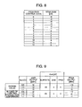
- FIG. 8 is a table showing the correspondence relation between control gains and gain control codes of FPGA stored in a register 252 ;
- FIG. 9 is a table showing the relation of input voltages of an amplifier 249 , output levels of amplifiers 242 a and 242 b and output levels of FPGA 246 ;
- FIG. 10 is a table showing an example of relation of gain control codes, control gains and output levels of FPGA.
- FIG. 11 is a table showing an example of relation of gain control codes, gains deviated from a design value and output levels of FPGA.
- FIG. 1 schematically illustrates an embodiment of a high-frequency integrated circuit (IC) to which the present invention is applied and which has a modulation/demodulation function of a transmission/reception signal and can make GMSK modulation in GSM system and 8-PSK modulation in EDGE system.
- the high-frequency IC 200 of the embodiment is constituted as a high-frequency IC of a multi-band system capable of making modulation/demodulation of signals in four frequency bands using three communication systems of GSM 850 and 900 , DCS (digital cellular system) 1800 and PCS (personal communications system) 1900 , although it is not limited thereto.
- the high-frequency IC 200 of the embodiment includes, when divided broadly, a receiving circuit RXC, a transmitting circuit TXC and a control circuit CTC including other circuits common to the transmitting and receiving circuits such as a controller and a clock generator.
- the receiving circuit RXC includes low-noise amplifiers 211 a , 211 b , 211 c and 211 d which amplify received signals of frequency bands for PCS, DCS and GSM, a frequency dividing and phase shifting circuit 210 which frequency-divides a local oscillation signal .phi.RF generated by a high-frequency oscillation circuit (RFVCO) described later to generate orthogonal signals having phases shifted by 90.degree.
- RFVCO high-frequency oscillation circuit
- a demodulation and frequency conversion unit 212 composed of mixers MIXa 1 , MIXa 2 , MIXb 1 , MIXb 2 , MIXc 1 , MIXc 2 , MIXd 1 and MIXd 2 which mix the received signals amplified by the low-noise amplifiers 211 a , 211 b , 211 c and 211 d with the orthogonal signals generated by the frequency-dividing and phase shifting circuit 210 to thereby make demodulation and down-conversion, high-gain amplifier circuits 213 A and 213 B which amplify demodulated I and Q signals, respectively, to be outputted to a baseband circuit 300 and are common to each band, and filters 214 A and 214 B which eliminate noise from the signals amplified by the high-gain amplifier circuits 213 A and 213 B.
- the receiving circuit RXC of the embodiment adopts a direct conversion system for down-converting the received signals to signals in the frequency band of the baseband directly.
- the control circuit CTC includes a controller (control logic) 260 which controls the whole chip, a reference oscillation circuit (DCXO) 261 which generates a reference oscillation signal .phi.ref, a high-frequency oscillation circuit (RFVCO) 262 constituting a local oscillation circuit which generates a high-frequency oscillation signal .phi.RF for frequency conversion, an RF synthesizer 263 constituting a PLL circuit together with the high-frequency oscillation circuit (RFVCO) 262 and a frequency dividing circuit 264 which frequency-divides the oscillation signal .phi.RF generated by the RFVCO 262 .
- a controller control logic
- DCXO reference oscillation circuit
- RFVCO high-frequency oscillation circuit
- RF synthesizer 263 constituting a PLL circuit together with the high-frequency oscillation circuit (RFVCO) 262 and a frequency dividing circuit 264 which frequency-divides the oscillation signal .phi.RF generated by the RFVCO 262 .
- the frequency dividing circuit 264 is controlled by a signal from the controller 260 and frequency-divides the oscillation signal .phi.RF by four in the GSM mode that transmission/reception is made in accordance with the GSM system and by two in the DCS or PCS system to be supplied to the transmitting circuit TXC.
- the controller 260 is supplied with a clock signal CLK for synchronization and a data signal DATA supplied from the baseband circuit and a load enable signal LEN supplied therefrom as a control signal.
- the load enable signal LEN is changed to an effective level, the controller 260 successively takes in the data signal DATA transmitted from the baseband circuit in synchronism with the clock signal CLK and generates a control signal used in chip in response to a command contained in the data signal DATA.
- the data signal DATA is transmitted serially, although it is not limited thereto.
- the RF synthesizer 263 is constituted by a frequency dividing circuit, a phase comparison circuit, a charging pump, a loop filter and the like.
- the transmitting circuit TXC includes an IFVCO 231 which generates an oscillation signal .phi.IF having an intermediate frequency such as, for example, 640 MHz, an IF synthesizer 232 constituting a PLL circuit together with the IFVCO 231 , a frequency dividing circuit 233 which frequency-divides the oscillation signal .phi.IF generated by the IFVCO 232 , a frequency dividing and phase shifting circuit 234 which further frequency-divides the signal frequency-divided by the frequency dividing circuit 233 and generates orthogonal signals (80 MHz) having phases shifted by 90.degree.
- an IFVCO 231 which generates an oscillation signal .phi.IF having an intermediate frequency such as, for example, 640 MHz
- an IF synthesizer 232 constituting a PLL circuit together with the IFVCO 231
- a frequency dividing circuit 233 which frequency-divides the oscillation signal .phi.IF generated by the IFVCO 232
- modulation circuits mixers
- 235 a and 235 b which modulate the generated orthogonal signals by I and Q signals supplied from the baseband circuit
- an adder 236 which combines the modulated signals
- a low pass filter (LPF) low pass filter
- TXVCO transmission oscillation circuit
- a frequency-dividing circuit 241 which frequency-divides the transmission signal .phi.TX outputted by the transmission oscillation circuit 240 to generate a transmission signal for the GSM system
- variable gain amplifiers (DMB) 242 a and 242 b which amplify the transmission signal
- output amplifiers TXVGA
- 243 a and 243 b constituted by variable gain amplifiers which further amplify the signals amplified by the variable gain amplifiers 242 a and 242 b to be outputted outside of a chip 200 .
- the transmitting circuit TXC includes buffers (attenuators) 244 a and 244 b which adjust (attenuate) amplitudes of the signals amplified by the variable gain amplifiers 242 a and 242 b to be fed back, an offset mixer 245 which mixes the feedback signal with a signal .phi.RF′ obtained by frequency-dividing the high-frequency oscillation signal .phi.RF generated by the high-frequency oscillation circuit (RFVCO) 262 to thereby generate a signal having a frequency corresponding to a difference between the frequencies thereof, a variable gain amplifier (FPGA) 246 which amplifies an output of the offset mixer 245 , a phase comparison circuit 237 which compares the feedback signal amplified by the variable gain amplifier (FPGA) 246 with a signal TXIF combined by the adder 236 to detect a phase difference, and a loop filter 238 which generates a voltage corresponding to an output of the phase detector 237 and supplies it to the transmission oscillation circuit (TXVCO) 240 as
- the phase comparison circuit 237 , the TXVCO 240 , the variable gain amplifiers 242 a , 242 b , the buffers 244 a , 244 b , the offset mixer 245 and the variable gain amplifier 246 constitute a phase control loop.
- the transmitting circuit TXC includes an amplitude comparison circuit 239 which compares the feedback signal amplified by the variable gain amplifier 246 with the signal TXIF combined by the adder 236 to detect an amplitude difference therebetween, a loop filter 247 for an amplitude control loop which limits a band of an output of the amplitude comparison circuit 239 , a variable gain amplifier (IPGA) 248 which amplifies a signal of the amplitude control loop, a fixed gain amplifier (LDO) 249 which is supplied with an output of the variable gain amplifier 248 and generates a control voltage supplied to the variable gain amplifier 242 a and 242 b connected to a succeeding stage of the TXVCO 240 , and a calibration execution circuit 250 which executes calibration of the amplitude control loop in accordance with the control signal supplied from the controller 260 .
- IPGA variable gain amplifier
- LDO fixed gain amplifier
- variable gain amplifier 242 a is to amplify the transmission signal on the low band side, that is, in the GSM of 850 to 900 MHz and the variable gain amplifier 242 b is to amplify the transmission signal on the high band side, that is, in the DCS of 1800 MHz and in the PCS of 1900 MHz.
- the transmitting circuit TXC of the embodiment adopts the offset PLL method in which the I and Q signals for transmission are orthogonally modulated by the carrier wave having the intermediate frequency and the feedback signal from the output side of the TXVCO 240 is mixed with the signal .phi.RF′ obtained by frequency-dividing the high-frequency oscillation signal .phi.RF of the RFVCO 262 to thereby be down-converted to the signal having the intermediate frequency corresponding to a frequency difference (offset), which signal is then phase-compared with the orthogonally modulated signal to control the TXVCO 240 in accordance with the phase difference.
- the transmitting circuit TXC of the embodiment further includes an error amplifier 270 which compares a signal RAMP indicating an output level from the baseband circuit with a detection signal DET from an output level detection circuit provided in a power module which power-amplifies the transmission signal outputted from the output amplifiers 243 a and 243 b to generate a control voltage Vapc which controls a gain of the output amplifiers 243 a and 243 b in accordance with a potential difference.
- the output amplifiers 243 a and 243 b has the variable gain width of about 60 dB.
- the controller 260 changes the frequency .phi.RF of the oscillation signal of the high-frequency oscillation circuit 262 upon transmission/reception in accordance with a band and a channel to be used in response to a command from the baseband circuit and changes a frequency ratio of the frequency dividing circuit 264 in accordance with the GSM mode or the DCS/PCS mode so that the frequency of the oscillation signal supplied to the receiving circuit RXC or the transmitting circuit TXC is changed to thereby change the frequency for transmission or reception.
- the oscillation frequency of the IFVCO 231 is set by the control signal from the controller 260 in accordance with the frequency to be used upon transmission.
- the controller 260 supplies the control signal for starting the calibration to the calibration execution circuit 250 .
- FIG. 2 is a block diagram showing a more concrete configuration example of the transmitting circuit TXC in the high-frequency IC of the embodiment.
- the transmitting circuit TXC of the embodiment includes two control loops of a feedback loop for phase control (phase control loop) and a feedback loop for amplitude control (amplitude control loop).
- phase control loop phase control loop
- amplitude control loop amplitude control loop
- FIG. 2 the configuration of the amplitude control loop characterizing the present invention is shown but the phase control loop is omitted.
- FIG. 2 the like circuits and elements to those shown in FIG. 1 are designated by like reference numeral and duplicated description thereof is omitted.
- the transmitting circuit TXC further includes, as circuits and elements not shown in FIG. 1 but shown in FIG. 2 , a calibration controller 251 , a register 252 which sets gains of the variable gain amplifier (IPGA) 248 on a forward path and the variable gain amplifier (FPGA) 246 on a feedback path and holds a measured value, an arithmetic circuit 253 which calculates the gain of the variable gain amplifier 246 from the measured value, a comparator 254 which detects an amplitude difference between a reference signal and the feedback signal, a change-over switch SW 1 which is disposed among a latch circuit 255 which holds a comparison result, the loop filter 247 and the variable gain amplifier (IPGA) 248 , and a change-over switch SW 2 which is connected between the variable gain amplifier (IPGA) 248 and the amplifier (LDO) 249 and can supply to the amplifier 249 a fixed DC voltage VDC instead of the output of the variable gain amplifier 248 .
- the switches SW 1 and SW 2 are formed of semiconductor.
- the calibration controller 251 , the register 252 , the arithmetic circuit 253 , the comparator 254 , the latch 255 and the change-over switches SW 1 and SW 2 constitutes the calibration execution circuit 250 of FIG. 1 .
- the calibration controller 251 may be integrated with the controller 260 of FIG. 1 .
- the change-over switches SW 1 and SW 2 are connected to form the amplitude control loop upon the normal operation (upon transmission) and the respective contacts of the switches SW 1 and SW 2 are connected to the comparator 254 and the fixed DC voltage VDC upon execution of the calibration, respectively.
- variable gain amplifier 242 b which amplifies the transmission signal on the high band, that is, in DCS and PCS is shown in FIG. 1 , although it is not shown in FIG. 2 . Since the amplitude control loop of the embodiment acts similarly even for the variable gain amplifier 242 b , only the variable gain amplifier (DMB) 242 a which amplifies the transmission signal on the low band, that is, in GSM is shown and the configuration and the operation of the calibration circuit of the amplitude control loop are now described.
- DMB variable gain amplifier
- Circuits on the amplitude control loop in the transmitting circuit TXC of the embodiment are constituted by differential circuits and signals on the forward path and the feedback path are transmitted as differential signals, although not clear in the drawing.
- dispersion in characteristic of an output voltage to a control voltage in the variable gain amplifier (DMB) 242 a having the gain controlled by a voltage from the forward path exerts largest influence on change of the loop band.
- DMB variable gain amplifier
- the IPGA 248 on the forward path utilizes the circuit using a variable current source as a current source of a general differential amplifier circuit composed of operation transistors Q 1 and Q 2 , collector resistors R 1 and R 2 and a constant current source CI as shown in FIG. 3A , for example, the gain thereof is difficult to be influenced by dispersion in characteristics of constituent elements in production. Further, since the IPGA 248 is operated in a relative low frequency band equal to or smaller than several MHz, deviation in characteristic from a design value is small and variation in gain upon operation is also small.
- the FPGA 246 Since the FPGA 246 has a higher operation frequency band as compared with the IPGA 248 , variation in gain upon operation is larger than the IPGA as far as the FPGA 246 is constituted by the same circuit as the IPGA.
- the FPGA 246 utilizes a differential amplifier circuit having emitter resistors R 3 and R 4 as shown in FIG. 3B , the gain thereof depends on a ratio of the emitter resistors R 3 , R 4 and the collector resistors R 1 , R 2 . Even if values of resistors on a chip of a semiconductor integrated circuit are dispersed, dispersion in a ratio of resistors is small and accordingly in the embodiment the FPGA 246 utilizes the differential amplifier circuit of FIG. 3B to thereby reduce variation in gain.
- the change-over switches SW 1 and SW 2 are disposed in the preceding stage and the succeeding stage of the IPGA 248 , respectively, to separate the IPGA 248 from the amplitude control loop upon calibration to make measurement. Consequently, it is not entirely necessary to consider how the gain of the IPGA is set upon calibration and calibration is made easily.
- the fixed gain amplifier (LDO) 249 can also utilizes a general differential amplifier circuit and the gain thereof is difficult to be influenced by dispersion in characteristics of constituent elements in production. Since the gain of the amplifier 249 is fixed, it is not necessary to consider change in gain upon calibration. Accordingly, the fixed DC voltage VDC is applied to the fixed gain amplifier (DMB) 242 a through the amplifier 249 to thereby make calibration in consideration of dispersion in gain of the amplifier 249 .
- two kinds of voltages of, for example, 0.9 V and 1.1 V are provided as the fixed DC voltage VDC supplied to the amplifier 249 by means of the switch SW 2 upon execution of calibration instead of the output voltage of the IPGA 248 .
- the gain of the amplitude control loop can be calibrated on the basis of the measured results at two voltage points of 0.9 V and 1.1 V to thereby execute relatively correct calibration in a short time.
- calibration of the gain of the amplitude control loop based on the measured results is attained by correcting values of gain control codes for the FPGA 246 and the IPGA 248 set to the register 252 .
- the comparator 254 compares the output voltage of the amplitude comparison circuit 239 with a predetermined reference voltage Vref to decide which amplitude of the reference signal and the feedback signal is larger.
- the amplitude comparison circuit 239 is a kind of mixer and outputs a voltage according to a difference between the reference signal and an amplitude component (envelope) of the feedback signal.
- the reference signal upon execution of calibration is a carrier signal which is obtained by inputting only the orthogonal signal from the frequency dividing and phase shifting circuit 234 to the modulation circuits (mixers) 235 a and 235 b and which is not subjected to modulation by the I and Q signals.
- calibration of the amplitude control loop may be automatically started in accordance with a micro-sequence in the calibration controller 251 by starting the calibration controller 251 by a reset signal produced in the chip in response to turning on of a power supply, for example.
- the calibration is started in response to a command supplied to the controller 260 from the external baseband circuit. Accordingly, in the high-frequency IC of the embodiment, the command can be inputted to thereby execute the calibration of the amplitude control loop at any time, although there is generally considered that it is sufficient that the calibration is executed only once upon turning on of the power supply.
- FIG. 4 shows a procedure of the calibration.
- the calibration according to the flow chart is started when a predetermined command code is supplied to the controller 260 from the baseband circuit. It is supposed that when an initialization command and initial values are supplied to the controller 260 from the baseband circuit before the calibration is started, a default value designating a gain of the variable gain amplifier (FPGA) 246 on the feedback path and a default value designating a gain of the variable gain amplifier (IPGA) 248 on the forward path are stored in the register 252 by the controller 260 .
- FPGA variable gain amplifier
- IPGA variable gain amplifier
- the default values are control codes designating gains decided as optimum values on the basis of characteristics of circuits constituting the amplitude control loop upon design of the circuits and there are four default values containing default values “FPGAG” and “IPGAG” for the circuit on the low band side and default values “FPGAD” and “IPGAD” for the circuit on the high band side. Further, it is supposed that a carrier signal which is not modulated is supplied to the amplitude comparison circuit 239 as a reference signal before the calibration is started.
- variable gain amplifier 242 b on the high band side is set to a stopped state and only the variable gain amplifier 242 a on the low band side is operated by the control signal from the calibration controller 251 (step S 1 ). Further, the control code “0” for setting the gain of FPGA 246 to be a minimum value is supplied to FPGA 246 (step S 2 ).
- the contacts of the change-over switches SW 1 and SW 2 which are usually connected to form the amplitude control loop are connected to the comparator 254 and the DC voltage VDC, respectively, to open the amplitude control loop.
- the DC voltage VDC is selectively set to a fixed voltage V such as 0.9 V which is a lower voltage within the range of voltages inputted to the amplifier (LDO) 249 upon usual operation and is applied to an input terminal of the amplifier 249 (step S 3 ).
- a fixed voltage V such as 0.9 V which is a lower voltage within the range of voltages inputted to the amplifier (LDO) 249 upon usual operation and is applied to an input terminal of the amplifier 249 (step S 3 ).
- the gain of FPGA 246 is first set to the minimum value by the control code “0”, the output of the comparator 254 is a low level.
- the control code designating the gain of FPGA 246 is increased by one level in step S 5 and the process is returned to step S 4 , in which whether the output polarity of the comparator 254 is inverted or not is decided.
- the control code at the time when the output polarity of the comparator 254 is inverted is stored in the register 252 as “FPGAG_V 1 ” (step S 6 ).
- control code “0” for setting the gain of FPGA 246 to be the minimum value is supplied to FPGA 246 (step S 7 ). Further, a fixed voltage V 2 such as 1.1V higher than the fixed voltage V 1 is selected as the DC voltage VDC and is supplied to the input terminal of the amplifier 249 (step S 8 ). In this state, whether the output voltage of the amplitude comparison circuit 239 which compares the reference signal with the feedback signal is larger than or equal to the reference voltage or not is decided on the basis of the output level of the comparator 254 (step S 9 ).
- step S 10 When the output of the comparator 254 is a low level, the control code designating the gain of FPGA 246 is increased by one level in step S 10 and then the process is returned to step S 9 , in which it is decided whether the output polarity of the comparator 254 is inverted or not.
- the control code at this time is stored in the register 252 as “FFPGAG_V 2 ” (step S 11 )
- the arithmetic circuit 253 calculates a difference Y from the codes “FPGAG_V 1 ” and “FPGAG_V 2 ” stored in the register 252 and also calculates a difference X between the difference Y of the measured values and the difference Y 0 of the design values (step S 12 ).
- the difference X is added to the default value “IPGAG” for the variable gain amplifier (IPGA) 248 on the forward path and its added result is stored in the register 252 as the gain setting code “IPGAG” for the IPGA 248 upon transmission operation (step S 13 ).
- the gain setting code of IPGA newly obtained may be overwritten on the default value previously stored in the register 252 or may be stored in a separate area.
- step S 14 the band in which the calibration is made is changed, that is, the variable gain amplifier 242 a on the low band side is set to the stopped state and the variable gain amplifier 242 b on the high band side is set to an operation state. Then, the process is returned to step S 2 and the above operation is repeated, so that the control codes “FPGAD_V 1 ” and “FPGAD_V 2 ” at the time when the output polarity of the comparator 254 is inverted is detected to be stored in the register 252 and the gain setting code “IPGAD” for the variable gain amplifier 242 b used upon transmission on the high band side is calculated from the codes “FPGAD_V 1 ” and “FPGAD_V 2 ” to be stored in the register 252 .
- the calibration is completed by the foregoing operation.
- the default values “FPGAG” and “FPGAD” are set as the gain control codes of FPGA 246 (step S 15 ). Consequently, even if the gain of the amplitude control loop is dispersed due to dispersion in characteristics of constituent elements in production, the gain of the IPGA 248 in the transmission operation is set so that deviation of the gain of the whole loop excluding the IPGA 248 is calibrated by the above calibration. Accordingly, the band of the amplitude control loop can approach a target value upon design, so that the modulation precision upon transmission can be enhanced and the noise suppression degree can be improved.
- the output level of the transmission oscillation circuit (TXVCO) 240 is +10 dBm
- the gain of the offset mixer 245 0 dB and the center gain of the FPGA 246 0 dB and the FPGA 246 has the gain control range of .+ ⁇ .6 dB in which the gain can be controlled in unit of 1 dB as shown in Table in FIG. 8 .
- the gain of the FPGA 246 is set to 0 dB of the center by the control code and when the gains of the respective circuits on the amplitude control loop are set as described above, the level of the feedback signal FB is ⁇ 5 dBm and can be matched to the level of the reference signal.
- the number of bits of the control code designating the gain of the FPGA 246 is decided in consideration of dispersion in gain of the amplitude control loop in production, the output levels of the amplifiers (DMB) 242 a , 242 b , the fixed voltage VDC applied through the switch SW 2 upon calibration and the gain control range and the unit of a controllable minimum gain (calibration precision) of the FPGA 246 .
- the gains of the circuits on the amplitude control loop are set as described above and the gain control range of the FPGA 246 is .+ ⁇ .6 dB in which the gain can be controlled in unit of 1 dB, the number of bits of the control code is 4.
- the gain control range and the unit of the controllable minimum gain of the IPGA 248 are preferably matched to those of the FPGA 246 and in this case the numbers of bits of the control loop for both of them are also equal to each other.
- FIG. 5 is a graph showing the relation between an input voltage VLDO of the amplifier (LDO) 249 and output amplitudes of the amplifier (DMB) 242 a , 242 b .
- solid line A represents a design value, that is, the characteristic at the time that it is assumed that there is no dispersion in characteristics of constituent elements in production
- one-dot chain line B represents the characteristic in case where the characteristic of the output voltage to the control voltage of the amplifiers (DMB) 242 a , 242 b is shifted or deviated to the low sensitivity due to dispersion in characteristics of constituent elements in production.
- FIG. 9 is a table showing the relation of the input voltage VLDO of the amplifier (LDO), the output level of the amplifiers (DMB) 242 a , 242 b and the output level of the FPGA 246 .
- the output levels of the amplifier (DMB) are 10, 13 and 15 dBm and the output levels of the FPGA are ⁇ 10, ⁇ 7 and ⁇ 5 dBm, respectively, whereas it is supposed that when the output voltage characteristic of the amplifier (DMB) is shifted or deviated as shown by one-dot chain line B due to dispersion in characteristics of constituent elements in production, the output levels of the amplifier (DMB) are as smaller than the design value as 10, 12 and 13 dBm and the output levels of the FPGA are also as smaller than the design value as ⁇ 10, ⁇ 8 and ⁇ 7 dBm, respectively.
- FIG. 10 shows an example of the relation of the control codes of FPGA, the gains of FPGA for the design values and the output levels of FPGA for the design values at the time that 0.9 and 1.1 V are inputted as the input voltages VLDC of the amplifier (LDO) 249 .
- FIG. 11 shows an example of the relation of the control codes of FPGA, the gains of FPGA when shifted or deviated from the design values and the measured output levels of FPGA at the time that 0.9 and 1.1 V are inputted to the amplifier (LDO) 249 .
- the gain control range and the unit of a controllable minimum gain of the IPGA 248 are matched to those of the FPGA 246 and accordingly when the gain setting code “IPGAG” of the IPGA is set to “8”, the gain of the IPGA is +2 dB from the table of FIG. 10 . That is, it is understood that when the gain of the FPGA 246 is reduced by ⁇ 2 dB due to dispersion in characteristics of constituent elements in production, the gain of the IPGA 248 is increased by 2 dB.
- the gain of the whole amplitude control loop that is, the loop band is kept substantially constant by the calibration regardless of dispersion in characteristics of constituent elements in production. Further, in the embodiment, since the calibration is automatically executed in the high-frequency IC upon turning on of a power supply or the like, it is not necessary to adjust the gain of the amplitude control loop individually after it is mounted in the system such as a portable telephone and the cost thereof can be reduced.
- the high-frequency IC is operated while maintained to a predetermined gain, that is, in the state where the input of the amplifier (LDO) 249 is not varied by applying a fixed voltage to the variable gain amplifier 242 a (or 242b) in the succeeding stage of the TXVCO 240 through the amplifier (LDO) 249 on the forward path of the amplitude control loop.
- the gains of the variable gain amplifier (PMB) 242 a and the variable gain amplifier (FPGA) 246 on the feedback path are deviated from the design values due to dispersion in characteristics of constituent elements in production, the phase control cannot be made with high accuracy and accordingly the calibration is required.
- the calibration according to the flow chart of FIG. 6 is executed.
- the calibration can be started by supplying a predetermined command code from the baseband circuit to the controller 260 . Further, similarly to the case of the EGDE modulation mode, it is supposed that the default value designating the gain of the variable gain amplifier (FPGA) 246 on the feedback path and the default value designating the gain of the variable gain amplifier (IPGA) 248 on the forward path are stored in the register 252 by the controller 260 before the calibration is started.
- FPGA variable gain amplifier
- IPGA variable gain amplifier
- variable gain amplifier 242 b on the high band side is set to the stopped state and the variable gain amplifier (DMB) 242 a on the low band side is set to the operation state by the control signal from the controller 251 (step S 21 ). Further, the control code “0” for setting the gain of the FPGA 246 to a minimum value is supplied to the FPGA 246 (step S 22 ).
- the contacts of the change-over switches SW 1 and SW 2 which are usually connected to form the amplitude control loop are connected to the comparator 254 and the DC voltage VDC, respectively, to open the amplitude control loop.
- the DC voltage VDC is selectively set to a value V 3 close to the voltage inputted to the amplifier (LDO) 249 when the transmission is made in the GMSK modulation mode and is applied to the input terminal of the amplifier 249 (step S 23 ).
- step S 24 whether the output voltage of the amplitude comparison circuit 239 which compares the reference signal with the feedback signal is larger than or equal to the reference voltage or not is decided on the basis of the output level of the comparator 254 (step S 24 ). Since the gain of the FPGA 246 is first set to a minimum value by the control code “0”, the output of the comparator 254 is a low level. In this case, the control code designating the gain of the FPGA 246 is increased by one level in step S 25 and the process is returned to step S 24 , in which it is decided whether the output polarity of the comparator 254 is inverted or not.
- the control code “FPGAG_V 3 ” of the gain of the FPGA 246 at this time is stored in the register 252 as the gain setting code “FPGAG” of the FPGA 246 in the transmission operation in the low band (step S 26 ).
- step S 21 the process is returned to step S 21 and the above operation is repeated, so that the control codes “FPGAD_V 3 ” at the time when the output polarity of the comparator 254 is inverted is stored in the register 252 as the gain setting code “FPGAD” of the FPGA 246 in the transmission operation in the high band.
- the design value of the output level of the FPGA 246 is ⁇ 5 dBm and if it is supposed that the actual gain of the FPGA 246 at this time is deviated by ⁇ 2 dB as shown by thick character in the table of FIG. 11 , the gain control code “FPGAG_V 3 ” at the time that the output polarity of the comparator 254 is inverted is “8”.
- the gain of the FPGA 246 is +2 dB and the output level of the FPGA is ⁇ 5 dBm.
- the gain of the FPGA 246 upon the transmission operation in the GMSK modulation mode is increased by 2 dB.
- the gain control code of the IPGA 248 upon the transmission operation in the GMSK modulation mode is the default value. Even if the gain of the FPGA 246 is dispersed due to dispersion in characteristics of constituent elements in production, the gain on the feedback path of the amplitude control loop is kept substantially constant by the calibration regardless of dispersion in characteristics of constituent elements in production.
- the difference X between the design value and the measured value calculated from the gain control codes “FPGAG_V 1 ” and “FPGAG_V 2 ” obtained by the calibration for the EDGE modulation mode is added to the default value “IPGAG” of the IPGA 248 on the forward path and its added result is used as the gain setting code “IPGAG” for the IPGA 248 .
- the gain control code “FPGAG_V 2 ” obtained by the calibration for the EDGE modulation mode is used as the gain control code of the FPGA 246 in the GMSK modulation mode.
- the IPGA 248 on the forward path is set to the off state even upon transmission and the switch SW 2 is connected to the DC voltage VDC similarly to the case where the calibration is made, so that the variable gain amplifier 242 a ( 242 b ) is supplied with the fixed voltage VLDO through the amplifier 249 to be operated with the gain fixed, while the FPGA 246 on the feedback path is set to the operation state since the phase control loop is required to be operated even in the GMSK modulation mode.
- FIG. 7 is a block diagram illustrating an example of a wireless communication system using the high-frequency IC of the embodiment.
- the wireless communication system includes a transmitting/receiving antenna 100 of radio signals, a switch 110 which changes over the antenna to make transmission and reception, high-frequency filters 120 a to 120 d constituted by SAW filters which remove unnecessary waves from a received signal, a high-frequency power amplifier circuit (power module) 130 which amplifies a transmission signal, the high-frequency IC 200 of the embodiment which demodulates a received signal and modulates a transmission signal, and a baseband circuit 300 which makes baseband processing such as conversion of audio signal and data signal to be transmitted into I signal of in-phase component to reference wave and Q signal of orthogonal component and conversion of received and modulated I and Q signals into audio signal and data signal and transmits a signal for controlling the high-frequency IC 200 .
- baseband circuit 300 which makes baseband processing such as conversion of audio signal and data signal to be transmitted into I signal of in-phase component to reference wave and Q signal of orthogonal component and conversion of received and modulated I and Q signals into audio signal and data signal and transmits a signal for controlling
- the high-frequency filters includes a filter 120 a for passing through a received signal in the frequency band of PCS 1900 , a filter 120 b for passing though a received signal in the frequency band of DCS 1800 , and filters 120 c and 120 d for passing through a received signal in the frequency band of GSM system.
- an SAW filter 140 is connected between a terminal of the high-frequency IC 200 from which a transmission signal of GSM system is outputted and the power module 130 .
- the high-frequency IC 200 and the baseband circuit 300 are formed on separate semiconductor chips as semiconductor integrated circuits.
- the high-frequency IC 200 and the filters 120 a to 120 d and 140 are mounted on an insulating substrate such as a ceramic substrate to be formed into a module 400 .
- a plurality of semiconductor chips and discrete components are mounted on an insulating substrate such as a ceramic substrate or a package having the surface and the inside in which printed wiring is formed and are connected by the printed wiring or bonding wire to fulfill a predetermined role to thereby be formed to be treated as one electronic component, which is named a module.
- the present invention made by the inventor has been described concretely on the basis of the embodiment, although it is needless to say that the present invention is not limited to the embodiment and various variations may be made thereto without departing from the spirit and scope of the invention.
- the default values of the control codes designating the gains of the variable gain amplifiers FPGA and IPGA in the high-frequency IC 200 are stored in the non-volatile memory in the baseband circuit 300 and are supplied to the high-frequency IC from the baseband circuit upon turning on of the power supply to be stored in the register 252 , although a non-volatile memory for storing the default values of the control codes designating the gains of the variable gain amplifiers FPGA and IPGA may be provided in the high-frequency IC.
- the calibration of the amplitude control loop is executed only once upon turning on of the power supply, although the calibration may be executed at any time during the period that transmitting/receiving operation is not made, such as a waiting time.
- the present invention is applied to a quadruple band system formed to be able to make communication for four bands in accordance with three communication systems of GSM 850 and 900 , DSC 1800 and PCS 1900 , although the present invention can be applied to a single band system which makes only communication in GSM system using modulation by GMSK modulation mode and 8-PSK modulation mode.
Abstract
Description
Claims (5)
Priority Applications (1)
| Application Number | Priority Date | Filing Date | Title |
|---|---|---|---|
| US12/263,571 US8095094B2 (en) | 2005-03-09 | 2008-11-03 | Communication semiconductor integrated circuit, communication electronic component and wireless communication system |
Applications Claiming Priority (5)
| Application Number | Priority Date | Filing Date | Title |
|---|---|---|---|
| GBP0504875.6 | 2005-03-09 | ||
| GB0504875A GB2424133B (en) | 2005-03-09 | 2005-03-09 | Communication semiconductor integrated circuit, communication electronic component and wireless communication system |
| GB0504875.6 | 2005-03-09 | ||
| US11/371,108 US7463876B2 (en) | 2005-03-09 | 2006-03-09 | Communication semiconductor integrated circuit, communication electronic component and wireless communication system |
| US12/263,571 US8095094B2 (en) | 2005-03-09 | 2008-11-03 | Communication semiconductor integrated circuit, communication electronic component and wireless communication system |
Related Parent Applications (1)
| Application Number | Title | Priority Date | Filing Date |
|---|---|---|---|
| US11/371,108 Continuation US7463876B2 (en) | 2005-03-09 | 2006-03-09 | Communication semiconductor integrated circuit, communication electronic component and wireless communication system |
Publications (2)
| Publication Number | Publication Date |
|---|---|
| US20090068967A1 US20090068967A1 (en) | 2009-03-12 |
| US8095094B2 true US8095094B2 (en) | 2012-01-10 |
Family
ID=34452089
Family Applications (2)
| Application Number | Title | Priority Date | Filing Date |
|---|---|---|---|
| US11/371,108 Expired - Fee Related US7463876B2 (en) | 2005-03-09 | 2006-03-09 | Communication semiconductor integrated circuit, communication electronic component and wireless communication system |
| US12/263,571 Expired - Fee Related US8095094B2 (en) | 2005-03-09 | 2008-11-03 | Communication semiconductor integrated circuit, communication electronic component and wireless communication system |
Family Applications Before (1)
| Application Number | Title | Priority Date | Filing Date |
|---|---|---|---|
| US11/371,108 Expired - Fee Related US7463876B2 (en) | 2005-03-09 | 2006-03-09 | Communication semiconductor integrated circuit, communication electronic component and wireless communication system |
Country Status (3)
| Country | Link |
|---|---|
| US (2) | US7463876B2 (en) |
| JP (1) | JP2006254405A (en) |
| GB (1) | GB2424133B (en) |
Cited By (2)
| Publication number | Priority date | Publication date | Assignee | Title |
|---|---|---|---|---|
| US20130094612A1 (en) * | 2009-12-21 | 2013-04-18 | Dali Systems Co. Ltd., Maples Corporate Services Limited | Multi-band wide band power amplifier digital predistortion system |
| US9548709B2 (en) | 2012-12-19 | 2017-01-17 | Qualcomm Incorporated | Independent gain control for multiple receive circuits concurrently processing different transmitted signals |
Families Citing this family (9)
| Publication number | Priority date | Publication date | Assignee | Title |
|---|---|---|---|---|
| GB2389251B (en) * | 2002-05-31 | 2005-09-07 | Hitachi Ltd | A communication semiconductor integrated circuit, a wireless communication apparatus, and a loop gain calibration method |
| GB2424133B (en) | 2005-03-09 | 2008-07-30 | Renesas Tech Corp | Communication semiconductor integrated circuit, communication electronic component and wireless communication system |
| US8457259B2 (en) * | 2006-07-17 | 2013-06-04 | Samsung Electronics Co., Ltd. | Method and system for partitioning gain for wireless radio frequency integrated circuits |
| US7729671B2 (en) * | 2006-12-06 | 2010-06-01 | Broadcom Corporation | Method and system for enhancing efficiency by modulating power amplifier gain |
| US8195105B1 (en) * | 2007-10-10 | 2012-06-05 | Rockwell Collins, Inc. | Power amplifier adaptive preset gain control |
| US7825740B2 (en) * | 2008-10-29 | 2010-11-02 | Texas Instruments Incorporated | Systems and methods for tracking communication parameters over a plurality of frequency bands |
| CN102324991B (en) * | 2011-08-16 | 2013-11-06 | 惠州Tcl移动通信有限公司 | Method for calibrating mobile terminal to transmit power in global system for mobile communication (GSM) frequency band |
| US20130043924A1 (en) * | 2011-08-16 | 2013-02-21 | The Aerospace Corporation | Systems, Methods, and Apparatus for High-Speed Signal Buffer Circuitry |
| US9190975B2 (en) * | 2013-09-27 | 2015-11-17 | Silicon Laboratories Inc. | Receiver chip with multiple independent loop-through paths |
Citations (8)
| Publication number | Priority date | Publication date | Assignee | Title |
|---|---|---|---|---|
| GB2389251A (en) | 2002-05-31 | 2003-12-03 | Hitachi Ltd | A polar-loop wireless communication apparatus, a semiconductor integrated circuit and a loop gain calibration method |
| GB2390495A (en) | 2002-07-05 | 2004-01-07 | Motorola Inc | Calibration of a transmitter or receiver in a transceiver wherein transmitter signals may be detected via the receiver or a separate detection arrangement |
| US20040012441A1 (en) | 2002-07-18 | 2004-01-22 | Mackey Christopher David | RF power amplifier digital gain flattening over multiband frequencies |
| GB2393595A (en) | 2002-09-26 | 2004-03-31 | Qualcomm | Calibration and control of gain and current of transmitter amplifier to improve linearity and efficiency |
| WO2004042919A1 (en) | 2002-11-04 | 2004-05-21 | Research In Motion Limited | Method and apparatus for regulating the transmitted power in multi-rate wireless communication systems |
| GB2424133A (en) | 2005-03-09 | 2006-09-13 | Renesas Tech Corp | Enhanced EDGE modulation precision through calibration of an aplitude control loop |
| US7132900B2 (en) | 2003-08-22 | 2006-11-07 | Renesas Technology Corp. | High frequency semiconductor integrated circuit device, wireless electric unit and wireless communication system |
| US7366481B2 (en) | 2002-05-31 | 2008-04-29 | Renesas Technology Corporation | Apparatus for radio telecommunication system and method of building up output power |
-
2005
- 2005-03-09 GB GB0504875A patent/GB2424133B/en not_active Expired - Fee Related
- 2005-10-26 JP JP2005310587A patent/JP2006254405A/en not_active Withdrawn
-
2006
- 2006-03-09 US US11/371,108 patent/US7463876B2/en not_active Expired - Fee Related
-
2008
- 2008-11-03 US US12/263,571 patent/US8095094B2/en not_active Expired - Fee Related
Patent Citations (9)
| Publication number | Priority date | Publication date | Assignee | Title |
|---|---|---|---|---|
| GB2389251A (en) | 2002-05-31 | 2003-12-03 | Hitachi Ltd | A polar-loop wireless communication apparatus, a semiconductor integrated circuit and a loop gain calibration method |
| US7082290B2 (en) | 2002-05-31 | 2006-07-25 | Renesas Technology Corp. | Communication semiconductor integrated circuit, a wireless communication apparatus, and a loop gain calibration method |
| US7366481B2 (en) | 2002-05-31 | 2008-04-29 | Renesas Technology Corporation | Apparatus for radio telecommunication system and method of building up output power |
| GB2390495A (en) | 2002-07-05 | 2004-01-07 | Motorola Inc | Calibration of a transmitter or receiver in a transceiver wherein transmitter signals may be detected via the receiver or a separate detection arrangement |
| US20040012441A1 (en) | 2002-07-18 | 2004-01-22 | Mackey Christopher David | RF power amplifier digital gain flattening over multiband frequencies |
| GB2393595A (en) | 2002-09-26 | 2004-03-31 | Qualcomm | Calibration and control of gain and current of transmitter amplifier to improve linearity and efficiency |
| WO2004042919A1 (en) | 2002-11-04 | 2004-05-21 | Research In Motion Limited | Method and apparatus for regulating the transmitted power in multi-rate wireless communication systems |
| US7132900B2 (en) | 2003-08-22 | 2006-11-07 | Renesas Technology Corp. | High frequency semiconductor integrated circuit device, wireless electric unit and wireless communication system |
| GB2424133A (en) | 2005-03-09 | 2006-09-13 | Renesas Tech Corp | Enhanced EDGE modulation precision through calibration of an aplitude control loop |
Cited By (5)
| Publication number | Priority date | Publication date | Assignee | Title |
|---|---|---|---|---|
| US20130094612A1 (en) * | 2009-12-21 | 2013-04-18 | Dali Systems Co. Ltd., Maples Corporate Services Limited | Multi-band wide band power amplifier digital predistortion system |
| US8467747B2 (en) * | 2009-12-21 | 2013-06-18 | Dali Systems Co. Ltd. | Multi-band wide band power amplifier digital predistortion system |
| US8903337B2 (en) | 2009-12-21 | 2014-12-02 | Dali Systems Co. Ltd. | Multi-band wide band power amplifier digital predistortion system |
| US9379745B2 (en) | 2009-12-21 | 2016-06-28 | Dali Systems Co. Ltd. | Multi-band wide band power amplifier digital predistortion system |
| US9548709B2 (en) | 2012-12-19 | 2017-01-17 | Qualcomm Incorporated | Independent gain control for multiple receive circuits concurrently processing different transmitted signals |
Also Published As
| Publication number | Publication date |
|---|---|
| US20090068967A1 (en) | 2009-03-12 |
| GB0504875D0 (en) | 2005-04-13 |
| GB2424133B (en) | 2008-07-30 |
| GB2424133A (en) | 2006-09-13 |
| US20060234656A1 (en) | 2006-10-19 |
| US7463876B2 (en) | 2008-12-09 |
| JP2006254405A (en) | 2006-09-21 |
Similar Documents
| Publication | Publication Date | Title |
|---|---|---|
| US8095094B2 (en) | Communication semiconductor integrated circuit, communication electronic component and wireless communication system | |
| US7082290B2 (en) | Communication semiconductor integrated circuit, a wireless communication apparatus, and a loop gain calibration method | |
| US7257385B2 (en) | Wireless communication semiconductor integrated circuit device and wireless communication system | |
| US7248842B2 (en) | Wireless communication apparatus having a phase control loop shared by first and second modulation modes and an amplitude control loop | |
| US7209717B2 (en) | Apparatus for radio telecommunication system and method of building up output power | |
| US7215215B2 (en) | Phase modulation apparatus, polar modulation transmission apparatus, wireless transmission apparatus and wireless communication apparatus | |
| US8315579B2 (en) | Semiconductor integrated circuit for communication | |
| US7454176B2 (en) | Semiconductor integrated circuit for communication and terminal device for mobile communication | |
| US7424276B2 (en) | Transmitter and wireless communication apparatus using the transmitter | |
| US20060234668A1 (en) | Communication semiconductor integrated circuit | |
| KR101498285B1 (en) | Transmitter and rf transmission signal processing circuit therefor, and transmitter operating method | |
| US20060234661A1 (en) | Semiconductor integrated circuit for communication and portable communication terminal | |
| US7515886B2 (en) | Digital broadcast receiving tuner and receiving device incorporating it | |
| KR20080059261A (en) | Single chip gsm/edge transceiver architecture with closed loop power control | |
| JP4245391B2 (en) | Wireless communication system and communication semiconductor integrated circuit | |
| US8131244B2 (en) | Method and system for dynamically adjusting intermediate frequency (IF) and filtering for microwave circuits | |
| JP2007174325A (en) | Semiconductor integrated circuit, calibration means of transmitter provided in same, and mobile communication equipment using same | |
| US20040266385A1 (en) | Semiconductor integrated circuit device and portable terminal system | |
| JP2002232318A (en) | Local oscillation circuit | |
| JPH10322237A (en) | Reception circuit |
Legal Events
| Date | Code | Title | Description |
|---|---|---|---|
| AS | Assignment |
Owner name: RENESAS ELECTRONICS CORPORATION, JAPAN Free format text: MERGER AND CHANGE OF NAME;ASSIGNOR:RENESAS TECHNOLOGY CORP.;REEL/FRAME:026287/0075 Effective date: 20100401 |
|
| STCF | Information on status: patent grant |
Free format text: PATENTED CASE |
|
| AS | Assignment |
Owner name: GOOGLE TECHNOLOGY HOLDINGS LLC, CALIFORNIA Free format text: ASSIGNMENT OF ASSIGNORS INTEREST;ASSIGNOR:MOTOROLA MOBILITY LLC;REEL/FRAME:035379/0116 Effective date: 20141028 |
|
| FPAY | Fee payment |
Year of fee payment: 4 |
|
| AS | Assignment |
Owner name: RENESAS ELECTRONICS CORPORATION, JAPAN Free format text: CHANGE OF ADDRESS;ASSIGNOR:RENESAS ELECTRONICS CORPORATION;REEL/FRAME:044928/0001 Effective date: 20150806 |
|
| FEPP | Fee payment procedure |
Free format text: MAINTENANCE FEE REMINDER MAILED (ORIGINAL EVENT CODE: REM.); ENTITY STATUS OF PATENT OWNER: LARGE ENTITY |
|
| LAPS | Lapse for failure to pay maintenance fees |
Free format text: PATENT EXPIRED FOR FAILURE TO PAY MAINTENANCE FEES (ORIGINAL EVENT CODE: EXP.); ENTITY STATUS OF PATENT OWNER: LARGE ENTITY |
|
| STCH | Information on status: patent discontinuation |
Free format text: PATENT EXPIRED DUE TO NONPAYMENT OF MAINTENANCE FEES UNDER 37 CFR 1.362 |
|
| FP | Lapsed due to failure to pay maintenance fee |
Effective date: 20200110 |