US8093579B2 - Semiconductor chip having a reduced band offset in its p-doped region and method for producing the semiconductor chip - Google Patents
Semiconductor chip having a reduced band offset in its p-doped region and method for producing the semiconductor chip Download PDFInfo
- Publication number
- US8093579B2 US8093579B2 US12/154,552 US15455208A US8093579B2 US 8093579 B2 US8093579 B2 US 8093579B2 US 15455208 A US15455208 A US 15455208A US 8093579 B2 US8093579 B2 US 8093579B2
- Authority
- US
- United States
- Prior art keywords
- interlayer
- material component
- semiconductor chip
- concentration
- contact layer
- Prior art date
- Legal status (The legal status is an assumption and is not a legal conclusion. Google has not performed a legal analysis and makes no representation as to the accuracy of the status listed.)
- Expired - Fee Related, expires
Links
- 239000004065 semiconductor Substances 0.000 title claims abstract description 106
- 238000004519 manufacturing process Methods 0.000 title claims abstract description 16
- 239000010410 layer Substances 0.000 claims abstract description 147
- 239000011229 interlayer Substances 0.000 claims abstract description 146
- 239000000463 material Substances 0.000 claims abstract description 104
- 238000005253 cladding Methods 0.000 claims abstract description 58
- 230000007423 decrease Effects 0.000 claims description 16
- 150000001875 compounds Chemical class 0.000 claims description 13
- 238000000034 method Methods 0.000 claims description 13
- OAICVXFJPJFONN-UHFFFAOYSA-N Phosphorus Chemical group [P] OAICVXFJPJFONN-UHFFFAOYSA-N 0.000 claims description 10
- 239000011777 magnesium Substances 0.000 claims description 10
- 229910052698 phosphorus Inorganic materials 0.000 claims description 10
- 239000011574 phosphorus Substances 0.000 claims description 10
- 229910052785 arsenic Inorganic materials 0.000 claims description 9
- RQNWIZPPADIBDY-UHFFFAOYSA-N arsenic atom Chemical compound [As] RQNWIZPPADIBDY-UHFFFAOYSA-N 0.000 claims description 9
- 229910052749 magnesium Inorganic materials 0.000 claims description 7
- 229910052725 zinc Inorganic materials 0.000 claims description 7
- 239000011701 zinc Substances 0.000 claims description 7
- 229910052782 aluminium Inorganic materials 0.000 claims description 6
- XAGFODPZIPBFFR-UHFFFAOYSA-N aluminium Chemical group [Al] XAGFODPZIPBFFR-UHFFFAOYSA-N 0.000 claims description 6
- 229910001218 Gallium arsenide Inorganic materials 0.000 claims description 5
- FYYHWMGAXLPEAU-UHFFFAOYSA-N Magnesium Chemical compound [Mg] FYYHWMGAXLPEAU-UHFFFAOYSA-N 0.000 claims description 5
- HCHKCACWOHOZIP-UHFFFAOYSA-N Zinc Chemical compound [Zn] HCHKCACWOHOZIP-UHFFFAOYSA-N 0.000 claims description 5
- 230000007704 transition Effects 0.000 claims description 5
- OKTJSMMVPCPJKN-UHFFFAOYSA-N Carbon Chemical compound [C] OKTJSMMVPCPJKN-UHFFFAOYSA-N 0.000 claims description 4
- GYHNNYVSQQEPJS-UHFFFAOYSA-N Gallium Chemical group [Ga] GYHNNYVSQQEPJS-UHFFFAOYSA-N 0.000 claims description 4
- RBFQJDQYXXHULB-UHFFFAOYSA-N arsane Chemical compound [AsH3] RBFQJDQYXXHULB-UHFFFAOYSA-N 0.000 claims description 4
- 229910052799 carbon Inorganic materials 0.000 claims description 4
- 229910052733 gallium Inorganic materials 0.000 claims description 4
- 229910052738 indium Inorganic materials 0.000 claims description 4
- APFVFJFRJDLVQX-UHFFFAOYSA-N indium atom Chemical group [In] APFVFJFRJDLVQX-UHFFFAOYSA-N 0.000 claims description 4
- 229910000980 Aluminium gallium arsenide Inorganic materials 0.000 claims description 3
- 239000002019 doping agent Substances 0.000 description 9
- 230000004888 barrier function Effects 0.000 description 8
- 230000008859 change Effects 0.000 description 7
- XYFCBTPGUUZFHI-UHFFFAOYSA-N Phosphine Chemical compound P XYFCBTPGUUZFHI-UHFFFAOYSA-N 0.000 description 6
- 230000009467 reduction Effects 0.000 description 5
- 229910000073 phosphorus hydride Inorganic materials 0.000 description 4
- 230000005855 radiation Effects 0.000 description 4
- 230000008901 benefit Effects 0.000 description 3
- 239000013078 crystal Substances 0.000 description 3
- 230000007547 defect Effects 0.000 description 3
- 239000000126 substance Substances 0.000 description 3
- 230000006978 adaptation Effects 0.000 description 1
- 230000002411 adverse Effects 0.000 description 1
- 230000001427 coherent effect Effects 0.000 description 1
- 239000000470 constituent Substances 0.000 description 1
- 238000001816 cooling Methods 0.000 description 1
- 238000000151 deposition Methods 0.000 description 1
- 238000010348 incorporation Methods 0.000 description 1
- 230000002045 lasting effect Effects 0.000 description 1
- 230000003446 memory effect Effects 0.000 description 1
- 229910052751 metal Inorganic materials 0.000 description 1
- 239000002184 metal Substances 0.000 description 1
- 238000001465 metallisation Methods 0.000 description 1
- 230000003287 optical effect Effects 0.000 description 1
- 230000000704 physical effect Effects 0.000 description 1
- 230000008569 process Effects 0.000 description 1
- 239000002096 quantum dot Substances 0.000 description 1
- 229910052710 silicon Inorganic materials 0.000 description 1
- 239000010703 silicon Substances 0.000 description 1
- 239000000758 substrate Substances 0.000 description 1
- 229910052714 tellurium Inorganic materials 0.000 description 1
- PORWMNRCUJJQNO-UHFFFAOYSA-N tellurium atom Chemical compound [Te] PORWMNRCUJJQNO-UHFFFAOYSA-N 0.000 description 1
- 238000000927 vapour-phase epitaxy Methods 0.000 description 1
Images


Classifications
-
- H—ELECTRICITY
- H01—ELECTRIC ELEMENTS
- H01S—DEVICES USING THE PROCESS OF LIGHT AMPLIFICATION BY STIMULATED EMISSION OF RADIATION [LASER] TO AMPLIFY OR GENERATE LIGHT; DEVICES USING STIMULATED EMISSION OF ELECTROMAGNETIC RADIATION IN WAVE RANGES OTHER THAN OPTICAL
- H01S5/00—Semiconductor lasers
- H01S5/30—Structure or shape of the active region; Materials used for the active region
- H01S5/305—Structure or shape of the active region; Materials used for the active region characterised by the doping materials used in the laser structure
-
- B—PERFORMING OPERATIONS; TRANSPORTING
- B82—NANOTECHNOLOGY
- B82Y—SPECIFIC USES OR APPLICATIONS OF NANOSTRUCTURES; MEASUREMENT OR ANALYSIS OF NANOSTRUCTURES; MANUFACTURE OR TREATMENT OF NANOSTRUCTURES
- B82Y20/00—Nanooptics, e.g. quantum optics or photonic crystals
-
- H—ELECTRICITY
- H01—ELECTRIC ELEMENTS
- H01L—SEMICONDUCTOR DEVICES NOT COVERED BY CLASS H10
- H01L29/00—Semiconductor devices adapted for rectifying, amplifying, oscillating or switching, or capacitors or resistors with at least one potential-jump barrier or surface barrier, e.g. PN junction depletion layer or carrier concentration layer; Details of semiconductor bodies or of electrodes thereof ; Multistep manufacturing processes therefor
- H01L29/02—Semiconductor bodies ; Multistep manufacturing processes therefor
- H01L29/12—Semiconductor bodies ; Multistep manufacturing processes therefor characterised by the materials of which they are formed
- H01L29/20—Semiconductor bodies ; Multistep manufacturing processes therefor characterised by the materials of which they are formed including, apart from doping materials or other impurities, only AIIIBV compounds
- H01L29/201—Semiconductor bodies ; Multistep manufacturing processes therefor characterised by the materials of which they are formed including, apart from doping materials or other impurities, only AIIIBV compounds including two or more compounds, e.g. alloys
- H01L29/205—Semiconductor bodies ; Multistep manufacturing processes therefor characterised by the materials of which they are formed including, apart from doping materials or other impurities, only AIIIBV compounds including two or more compounds, e.g. alloys in different semiconductor regions, e.g. heterojunctions
-
- H—ELECTRICITY
- H01—ELECTRIC ELEMENTS
- H01L—SEMICONDUCTOR DEVICES NOT COVERED BY CLASS H10
- H01L33/00—Semiconductor devices with at least one potential-jump barrier or surface barrier specially adapted for light emission; Processes or apparatus specially adapted for the manufacture or treatment thereof or of parts thereof; Details thereof
- H01L33/02—Semiconductor devices with at least one potential-jump barrier or surface barrier specially adapted for light emission; Processes or apparatus specially adapted for the manufacture or treatment thereof or of parts thereof; Details thereof characterised by the semiconductor bodies
- H01L33/14—Semiconductor devices with at least one potential-jump barrier or surface barrier specially adapted for light emission; Processes or apparatus specially adapted for the manufacture or treatment thereof or of parts thereof; Details thereof characterised by the semiconductor bodies with a carrier transport control structure, e.g. highly-doped semiconductor layer or current-blocking structure
-
- H—ELECTRICITY
- H01—ELECTRIC ELEMENTS
- H01S—DEVICES USING THE PROCESS OF LIGHT AMPLIFICATION BY STIMULATED EMISSION OF RADIATION [LASER] TO AMPLIFY OR GENERATE LIGHT; DEVICES USING STIMULATED EMISSION OF ELECTROMAGNETIC RADIATION IN WAVE RANGES OTHER THAN OPTICAL
- H01S5/00—Semiconductor lasers
- H01S5/30—Structure or shape of the active region; Materials used for the active region
- H01S5/32—Structure or shape of the active region; Materials used for the active region comprising PN junctions, e.g. hetero- or double- heterostructures
-
- H—ELECTRICITY
- H01—ELECTRIC ELEMENTS
- H01L—SEMICONDUCTOR DEVICES NOT COVERED BY CLASS H10
- H01L2924/00—Indexing scheme for arrangements or methods for connecting or disconnecting semiconductor or solid-state bodies as covered by H01L24/00
- H01L2924/0001—Technical content checked by a classifier
- H01L2924/0002—Not covered by any one of groups H01L24/00, H01L24/00 and H01L2224/00
-
- H—ELECTRICITY
- H01—ELECTRIC ELEMENTS
- H01L—SEMICONDUCTOR DEVICES NOT COVERED BY CLASS H10
- H01L33/00—Semiconductor devices with at least one potential-jump barrier or surface barrier specially adapted for light emission; Processes or apparatus specially adapted for the manufacture or treatment thereof or of parts thereof; Details thereof
- H01L33/02—Semiconductor devices with at least one potential-jump barrier or surface barrier specially adapted for light emission; Processes or apparatus specially adapted for the manufacture or treatment thereof or of parts thereof; Details thereof characterised by the semiconductor bodies
- H01L33/025—Physical imperfections, e.g. particular concentration or distribution of impurities
-
- H—ELECTRICITY
- H01—ELECTRIC ELEMENTS
- H01L—SEMICONDUCTOR DEVICES NOT COVERED BY CLASS H10
- H01L33/00—Semiconductor devices with at least one potential-jump barrier or surface barrier specially adapted for light emission; Processes or apparatus specially adapted for the manufacture or treatment thereof or of parts thereof; Details thereof
- H01L33/02—Semiconductor devices with at least one potential-jump barrier or surface barrier specially adapted for light emission; Processes or apparatus specially adapted for the manufacture or treatment thereof or of parts thereof; Details thereof characterised by the semiconductor bodies
- H01L33/26—Materials of the light emitting region
- H01L33/30—Materials of the light emitting region containing only elements of group III and group V of the periodic system
-
- H—ELECTRICITY
- H01—ELECTRIC ELEMENTS
- H01S—DEVICES USING THE PROCESS OF LIGHT AMPLIFICATION BY STIMULATED EMISSION OF RADIATION [LASER] TO AMPLIFY OR GENERATE LIGHT; DEVICES USING STIMULATED EMISSION OF ELECTROMAGNETIC RADIATION IN WAVE RANGES OTHER THAN OPTICAL
- H01S2304/00—Special growth methods for semiconductor lasers
- H01S2304/04—MOCVD or MOVPE
-
- H—ELECTRICITY
- H01—ELECTRIC ELEMENTS
- H01S—DEVICES USING THE PROCESS OF LIGHT AMPLIFICATION BY STIMULATED EMISSION OF RADIATION [LASER] TO AMPLIFY OR GENERATE LIGHT; DEVICES USING STIMULATED EMISSION OF ELECTROMAGNETIC RADIATION IN WAVE RANGES OTHER THAN OPTICAL
- H01S5/00—Semiconductor lasers
- H01S5/30—Structure or shape of the active region; Materials used for the active region
- H01S5/305—Structure or shape of the active region; Materials used for the active region characterised by the doping materials used in the laser structure
- H01S5/3054—Structure or shape of the active region; Materials used for the active region characterised by the doping materials used in the laser structure p-doping
- H01S5/3063—Structure or shape of the active region; Materials used for the active region characterised by the doping materials used in the laser structure p-doping using Mg
-
- H—ELECTRICITY
- H01—ELECTRIC ELEMENTS
- H01S—DEVICES USING THE PROCESS OF LIGHT AMPLIFICATION BY STIMULATED EMISSION OF RADIATION [LASER] TO AMPLIFY OR GENERATE LIGHT; DEVICES USING STIMULATED EMISSION OF ELECTROMAGNETIC RADIATION IN WAVE RANGES OTHER THAN OPTICAL
- H01S5/00—Semiconductor lasers
- H01S5/30—Structure or shape of the active region; Materials used for the active region
- H01S5/32—Structure or shape of the active region; Materials used for the active region comprising PN junctions, e.g. hetero- or double- heterostructures
- H01S5/321—Structure or shape of the active region; Materials used for the active region comprising PN junctions, e.g. hetero- or double- heterostructures having intermediate bandgap layers
-
- H—ELECTRICITY
- H01—ELECTRIC ELEMENTS
- H01S—DEVICES USING THE PROCESS OF LIGHT AMPLIFICATION BY STIMULATED EMISSION OF RADIATION [LASER] TO AMPLIFY OR GENERATE LIGHT; DEVICES USING STIMULATED EMISSION OF ELECTROMAGNETIC RADIATION IN WAVE RANGES OTHER THAN OPTICAL
- H01S5/00—Semiconductor lasers
- H01S5/30—Structure or shape of the active region; Materials used for the active region
- H01S5/32—Structure or shape of the active region; Materials used for the active region comprising PN junctions, e.g. hetero- or double- heterostructures
- H01S5/3211—Structure or shape of the active region; Materials used for the active region comprising PN junctions, e.g. hetero- or double- heterostructures characterised by special cladding layers, e.g. details on band-discontinuities
- H01S5/3213—Structure or shape of the active region; Materials used for the active region comprising PN junctions, e.g. hetero- or double- heterostructures characterised by special cladding layers, e.g. details on band-discontinuities asymmetric clading layers
-
- H—ELECTRICITY
- H01—ELECTRIC ELEMENTS
- H01S—DEVICES USING THE PROCESS OF LIGHT AMPLIFICATION BY STIMULATED EMISSION OF RADIATION [LASER] TO AMPLIFY OR GENERATE LIGHT; DEVICES USING STIMULATED EMISSION OF ELECTROMAGNETIC RADIATION IN WAVE RANGES OTHER THAN OPTICAL
- H01S5/00—Semiconductor lasers
- H01S5/30—Structure or shape of the active region; Materials used for the active region
- H01S5/32—Structure or shape of the active region; Materials used for the active region comprising PN junctions, e.g. hetero- or double- heterostructures
- H01S5/3211—Structure or shape of the active region; Materials used for the active region comprising PN junctions, e.g. hetero- or double- heterostructures characterised by special cladding layers, e.g. details on band-discontinuities
- H01S5/3215—Structure or shape of the active region; Materials used for the active region comprising PN junctions, e.g. hetero- or double- heterostructures characterised by special cladding layers, e.g. details on band-discontinuities graded composition cladding layers
-
- H—ELECTRICITY
- H01—ELECTRIC ELEMENTS
- H01S—DEVICES USING THE PROCESS OF LIGHT AMPLIFICATION BY STIMULATED EMISSION OF RADIATION [LASER] TO AMPLIFY OR GENERATE LIGHT; DEVICES USING STIMULATED EMISSION OF ELECTROMAGNETIC RADIATION IN WAVE RANGES OTHER THAN OPTICAL
- H01S5/00—Semiconductor lasers
- H01S5/30—Structure or shape of the active region; Materials used for the active region
- H01S5/34—Structure or shape of the active region; Materials used for the active region comprising quantum well or superlattice structures, e.g. single quantum well [SQW] lasers, multiple quantum well [MQW] lasers or graded index separate confinement heterostructure [GRINSCH] lasers
- H01S5/343—Structure or shape of the active region; Materials used for the active region comprising quantum well or superlattice structures, e.g. single quantum well [SQW] lasers, multiple quantum well [MQW] lasers or graded index separate confinement heterostructure [GRINSCH] lasers in AIIIBV compounds, e.g. AlGaAs-laser, InP-based laser
- H01S5/34346—Structure or shape of the active region; Materials used for the active region comprising quantum well or superlattice structures, e.g. single quantum well [SQW] lasers, multiple quantum well [MQW] lasers or graded index separate confinement heterostructure [GRINSCH] lasers in AIIIBV compounds, e.g. AlGaAs-laser, InP-based laser characterised by the materials of the barrier layers
- H01S5/3436—Structure or shape of the active region; Materials used for the active region comprising quantum well or superlattice structures, e.g. single quantum well [SQW] lasers, multiple quantum well [MQW] lasers or graded index separate confinement heterostructure [GRINSCH] lasers in AIIIBV compounds, e.g. AlGaAs-laser, InP-based laser characterised by the materials of the barrier layers based on InGa(Al)P
Definitions
- the invention relates to a semiconductor chip and a method for producing a semiconductor chip of this type.
- a p-side contact layer can comprise p-doped GaAs.
- the p-doped GaAs is usually deposited at a temperature that is lower than the production temperature of preceding layers. Cooling to this temperature is typically effected under PH 3 supporting pressure. A high charge of PH 3 into a reactor chamber which is caused in this way can have adverse consequences for the crystal quality of the further growth on account of the high vapour pressure of phosphorus.
- a high band offset typically occurs at a transition from the contact layer to a cladding layer. Said band offset is generally reduced by a p-doped interlayer containing InGaP. Nevertheless, stepped barriers can still occur which make hole conduction more difficult (cf. FIG. 7A ). This is because although an extent of the barriers can be reduced by means of doping, the height of said barriers cannot be reduced.
- a further object of the present invention is to provide a simplified method for producing a semiconductor chip of this type.
- a semiconductor chip comprising a p-doped region having a cladding layer and a contact layer, wherein a first interlayer and a second interlayer are arranged between the cladding layer and the contact layer, and wherein a concentration y of a first material component within the first and the second interlayer changes in such a way that the band gap within the first and the second interlayer varies in a range lying between the band gap of the cladding layer and the band gap of the contact layer.
- An abrupt change in the size of the band gap at the transition from the contact layer to the cladding layer can advantageously be prevented by means of the first and second interlayers. This is because the first and the second interlayer enable a gradual adaptation of the size of the band gap between the contact layer and the cladding layer.
- the size of the band gap within the first interlayer decreases proceeding from the cladding layer toward the second interlayer. This can be achieved in particular by virtue of the fact that the concentration y of the first material component within the first interlayer decreases proceeding from the cladding layer toward the second interlayer. This configuration has the consequence that the voltage drop in the current flow direction is reduced and the series resistance of the semiconductor chip is significantly smaller than in the case of a conventional semiconductor chip.
- the band gap within the second interlayer preferably decreases proceeding from the first interlayer toward the contact layer. Particularly preferably, this is achieved by virtue of the fact that the concentration y of the first material component within the second interlayer decreases proceeding from the first interlayer toward the contact layer. In this case, too, a gradual change in the size of the band gap or in the concentration of the first material component can bring about a reduction of the series resistance of the semiconductor chip.
- a respective compound semiconductor material is used for the cladding layer, the first interlayer, the second interlayer and the contact layer.
- Said compound semiconductor material can be a III-V compound semiconductor material, in particular.
- the compound semiconductor material of the first interlayer is a quaternary compound semiconductor material, in particular a phosphide-based semiconductor material
- the compound semiconductor material of the second interlayer is a ternary compound semiconductor material, in particular an arsenide-based semiconductor material.
- the cladding layer can comprise a phosphide-based semiconductor material, while the contact layer contains an arsenide-based semiconductor material.
- a composition of the respective compound semiconductor material can be described by the following formula: C x B y(1-x) E (1-y)(1-x) A, where 0 ⁇ x ⁇ 1 and 0 ⁇ y ⁇ 1.
- the letters A, B, C, E stand for the individual material components of which the compound semiconductor material is composed. In this case, this material need not necessarily have a mathematically exact composition according to the above formula. Rather, it can have one or more dopants and additional constituents which essentially do not change the physical properties, in particular the crystal structure or band structure, of the material.
- the first material component (B) can be aluminum
- a second material component (E) can be gallium
- a third material component (C) can be indium
- a fourth material component (A) can be phosphorus or arsenic.
- the concentration x of the third material component can be constant in this case.
- the concentration x of the third material component can vary.
- the concentration of the first material component and that of the second material component are understood to mean the parameters y and 1-y respectively. It is apparent that the parameter x must also be taken into account for precise calculation of the material composition.
- the cladding layer can contain InAlP, while the contact layer comprises GaAs.
- the band gap can be varied in a range lying between the band gap of the cladding layer and that of the contact layer.
- the content of the first material component or the aluminum content at the interface between the first and the second interlayer is preferably chosen in such a way that an energy barrier that has to be surmounted by the holes is comparatively small.
- the cladding layer contains InAlP
- the first interlayer contains InAlGaP
- the second interlayer contains AlGaAs
- the contact layer contains GaAs.
- the concentration y of the first material component within the first interlayer, on a side facing the cladding layer is between 20% and 100% inclusive.
- the concentration y can be between 70% and 90% inclusive.
- the concentration y of the first material component within the first interlayer, on a side facing the second interlayer falls to a value of between 0% and 50% inclusive.
- the concentration y of the first material component within the first interlayer, on a side facing the second interlayer can fall to a value of between 10% and 40% inclusive.
- a valence band has a continuous profile proceeding from the cladding layer towards the contact layer.
- the profile of the concentration y of the first material component in a growth direction in which the layers have grown, within the first interlayer can be like a straight line having a gradient not equal to zero, that is to say that the concentration changes continuously in the growth direction and has a linear profile, in particular.
- a stepped change in the concentration is also conceivable.
- the concentration y of the first material component within the second interlayer, on a side facing the first interlayer is between 10% and 100% inclusive.
- the concentration y of the first material component within the second interlayer, on a side facing the first interlayer can be between 60% and 80% inclusive.
- the concentration y of the first material component within the second interlayer, on a side facing the contact layer preferably falls to a value of between 0% and 50% inclusive.
- the concentration y of the first material component within the second interlayer, on a side facing the contact layer can fall to a value of between 2% and 5% inclusive.
- the concentration y can decrease continuously, in particular linearly, or in stepped fashion.
- the semiconductor chip has, in particular, an active region arranged between the p-doped region and an n-doped region.
- radiation is generated in the active region during operation of the semiconductor chip. Consequently, the semiconductor chip can be referred to as a radiation-emitting semiconductor chip.
- the active region preferably comprises a radiation-generating pn junction.
- said pn junction can be formed by means of a p-conducting and an n-conducting semiconductor layer that directly adjoin one another.
- the actual radiation-generating layer for instance in the form of a doped or undoped quantum layer, is formed between the p-conducting and the n-conducting active layer.
- the quantum layer can be shaped as a single quantum well structure (SQW) or multiple quantum well structure (MQW) or else as a quantum wire or quantum dot structure.
- the semiconductor chip is a laser diode chip.
- the semiconductor chip generates coherent radiation in this case.
- the semiconductor chip can generate incoherent radiation for example in the configuration as a light-emitting diode.
- Another aspect of the present invention is directed to a method for producing a semiconductor chip in accordance with one of the variants described above.
- the method comprises the following steps:
- the second interlayer is grown onto the first interlayer without any interruption of growth.
- the production time for the semiconductor chip can advantageously be shortened as a result of this.
- the second interlayer can also be grown onto the first interlayer with interruption of growth.
- the semiconductor chip is preferably produced by means of MOVPE.
- the atmosphere in which the first interlayer is grown is free of arsenic-containing substances.
- the atmosphere in which the second interlayer is grown is preferably free of phosphorus-containing substances.
- the first and the second interlayer can be grown at the same temperature.
- the temperature can be approximately 700° C.
- An interruption of growth preferably takes place after the second interlayer has been grown, the temperature being reduced within said interruption of growth.
- the interruption of growth can last for a number of minutes.
- the temperature reduction does not take under phosphine supporting pressure with the disadvantages mentioned at the beginning, but rather under arsine supporting pressure.
- This has the advantage, firstly, that the semiconductor chip has an improved morphology and, secondly, that a memory effect is significantly suppressed.
- the contact layer is grown after the interruption of growth. This can be carried out at a temperature of approximately 550° C.
- a temperature reduction can begin as early as when growing the first and/or second interlayer. This has the advantage that it is possible to dispense with the interruption of growth prior to growing the contact layer, or that the interruption of growth can be shortened.
- the p-doped region can be doped by means of various dopants.
- the cladding layer and the first interlayer can be doped with magnesium or zinc.
- carbon as well as zinc or magnesium are particularly suitable as dopants for the second interlayer and the contact layer.
- the growth of the second interlayer which preferably contains AlGaAs, even at high temperatures advantageously enables a sufficiently high incorporation of carbon, magnesium or zinc into the second interlayer. Therefore, the changeover from phosphorus-based growth to arsenic-based growth can take place at high temperatures without any interruption of growth. As a result, the electrical properties of the semiconductor chip can be significantly improved since hole conduction is improved and the series resistance is reduced.
- the concentration of the first material component in the atmosphere is reduced continuously in the course of growing the first and the second interlayer.
- FIG. 1 shows a schematic cross-sectional view of an exemplary embodiment of a semiconductor chip according to the invention
- FIG. 2 shows a schematic cross-sectional view of an exemplary embodiment of a conventional semiconductor chip
- FIG. 3 shows a graph illustrating the defect density D of the semiconductor chip according to the invention and of the conventional semiconductor chip
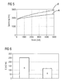
- FIG. 5 shows a graph illustrating current-voltage curves of the semiconductor chip according to the invention and of the conventional semiconductor chip
- FIGS. 8A to 8D show a schematic illustration of different method steps for producing a semiconductor chip according to the invention.
- the semiconductor chip 1 illustrated in FIG. 1 comprises a semiconductor layer sequence 23 , which on the rear side is arranged on a carrier 2 and on the front side is provided with a contact metallization 3 for making electrical contact with the semiconductor chip 1 .
- the carrier 2 can be a growth substrate used for growing the layer sequence 23 or alternatively a mounting body to which the layer sequence 23 was applied after production. Furthermore, a further electrical contact can be provided on the carrier 2 .
- the p-doped region I comprises a cladding layer 18 , a first interlayer 19 , a second interlayer 20 and a contact layer 21 .
- the active region II comprises an undoped quantum well layer 16 and barrier layers 15 and 17 , which are likewise undoped.
- Adjacent to the active region II is the n-doped region III, which has a doped barrier layer 14 , a cladding layer 13 and also an interlayer 12 and a contact layer 11 .
- Preferred dopants for the n-type doping are silicon and tellurium.
- Mg or Zn is used for the p-type doping in the cladding layer 18 and in the first interlayer 19
- C is used for the p-type doping of the second interlayer 20 and of the contact layer 21 . It is also possible, however, to use Mg or Zn in the second interlayer 20 and the contact layer 21 .
- the Al concentration y is at a maximum with 100% in the cladding layer 18 , while it assumes a minimum value of 0% in the contact layer 21 .
- the Al concentration y decreases proceeding from the cladding layer 18 towards the second interlayer 20 from 70% to 20%. The decrease preferably takes place continuously within the first interlayer 19 and does not continue right into the second interlayer 20 . Rather, in the second interlayer 20 the Al concentration y starts at a new value that is higher than the final value of the Al concentration y in the first interlayer 19 and is 60% here. In the second interlayer 20 the Al concentration y decreases, preferably continuously, down to a value of 5%.
- first interlayer 19 and the second interlayer 20 it is possible to reduce a band offset between the cladding layer 18 and the contact layer 21 , that is to say the size difference in the band gap between the cladding layer 18 and the contact layer 21 , in comparison with a conventional semiconductor chip.
- FIG. 2 illustrates a conventional semiconductor chip 1 for comparison, said chip having a p-doped interlayer 24 with no Al content instead of the first and the second interlayer.
- FIG. 3 shows a graph with values of the defect density D which occur in the case (A) of the semiconductor chip according to the invention in accordance with the exemplary embodiment illustrated in FIG. 1 and in the case (B) of the conventional semiconductor chip in accordance with the exemplary embodiment illustrated in FIG. 2 .
- the value in the case of the semiconductor chip illustrated in FIG. 2 (26 cm ⁇ 2 ) is approximately a factor of 5 higher than in the case of the semiconductor chip in accordance with FIG. 1 (5 cm ⁇ 2 ).
- a lower defect density D has the advantage that the lifetime of the semiconductor chip can be increased.
- the graph of FIG. 5 shows current-voltage characteristic curves for the semiconductor chip in accordance with the exemplary embodiment (A) illustrated in FIG. 1 and the semiconductor chip in accordance with the exemplary embodiment (B) illustrated in FIG. 2 .
- a smaller rise in the voltage as the current increases can be noted in the case of the semiconductor chip in accordance with FIG. 1 . Consequently, the semiconductor chip in accordance with FIG. 1 requires a lower electrical power for the same optical output power.
- the graph of FIG. 6 plots values for the electrical resistance E of the semiconductor chip in accordance with the exemplary embodiment (A) illustrated in FIG. 1 and the semiconductor chip in accordance with the exemplary embodiment (B) illustrated in FIG. 2 . From the graph, a value (252 mohms) that is approximately double the value (119 mohms) of the semiconductor chip in accordance with FIG. 1 can be inferred for the semiconductor chip in accordance with FIG. 2 .
- a reduction of the electrical resistance E leads to the reduction, already mentioned in connection with FIG. 5 , of the electrical power consumption in the case of the semiconductor chip in accordance with FIG. 1 .
- the epitaxial layers are grown by means of MOVPE.
- FIG. 8A shows a production step for growing the p-doped cladding layer (cf. FIG. 1 , cladding layer 18 ).
- the material components A, B, C and D required for this are introduced in a gaseous state into a reactor chamber 22 through corresponding supply lines.
- the material component A corresponds to a phosphorus-containing gas, in particular phosphine
- the material component B corresponds to an aluminum-containing gas
- the material component C corresponds to an indium-containing gas
- the material component D corresponds to a first p-type dopant, in particular Mg.
- the p-doped cladding layer is grown at a temperature of between approximately 700° C. and 800° C.
- the layers 11 to 17 , on which the p-doped cladding layer is deposited, are also produced at said temperature.
- the resulting p-doped cladding layer has the properties indicated in the table for the layer 18 .
- FIG. 8B schematically illustrates a production step for depositing the first interlayer (cf. FIG. 1 , first interlayer 19 ).
- a further material component E is supplied, which corresponds to a gallium-containing gas.
- the growth temperature does not change in comparison with the preceding production step ( Figure A).
- the concentration of the material component B as emerges from the table for the first interlayer 19 , continuously decreases.
- the concentration of the material component E is simultaneously increased.
- the concentration of the material component D that is to say of the p-type dopant, is increased.
- the second interlayer (cf. FIG. 1 , second interlayer 20 ) is grown in a next production step, illustrated in FIG. 8C .
- the material components B and E continue to be introduced into the reactor chamber 22 .
- the material component C is omitted, by contrast.
- the material component A is replaced by the material component F, which need not necessarily be passed through the same supply line as the material component A.
- the material component F is an arsenic-containing gas, in particular arsine.
- the changeover from phosphorus-based growth to arsenic-based growth is performed instantaneously, that is to say that the switching off of a phosphorus-containing gas source takes place at the same time as the switching on of an arsenic-containing gas source.
- the concentration of the material component B is continuously reduced and the concentration of the material component E is continuously increased (cf. table, second interlayer 20 ).
- the material component G is added, which corresponds to a second dopant, in particular carbon. As can be seen from the table, the material component G is continuously increased.
- a growth pause, lasting a few minutes, of preferably 3 min to 5 min is introduced between the production steps illustrated in FIG. 8C and FIG. 8D .
- the temperature is reduced to approximately 540° C., which is preferably done under arsine supporting pressure.
- the p-doped contact layer (cf. FIG. 1 , contact layer 21 ) is then grown from the material components G and E and p-doped with the material component F. More detailed information in this respect can be found in the table.
Abstract
Description
| Dopant | |||||
| Al concen- | Ga concen- | Thickness | concentration | ||
| tration y [%] | tration 1-y [%] | [nm] | [n/cm3] | ||
| |
200 | 2.4*1018 (Si) | ||
| |
40 | 60 | 200 | 2.9*1018 (Si) |
| |
100 | 0 | 800 | 2.0*1018 (Si) |
| |
40 | 60 | 20 | 2.1*1018 (Si) |
| |
40 | 60 | 230 | |
| |
5 | |||
| |
40 | 60 | 250 | |
| |
100 | 0 | 800 | 2.9*1017 (Mg) |
| |
70 → 20 | 30 → 80 | 20 | 1.1*1017 → |
| 2.9*1017 (Mg) | ||||
| |
60 → 5 | 40 → 95 | 60 | 3.7*1018 → |
| 1.1*1019 (C) | ||||
| |
0 | 100 | 400 | 1*1020-2*1020 (C) |
Claims (31)
CxBy(1-x)E(1-y)(1-x)A, where 0≦x≦1 and 0≦y≦1;
CxBy(1-x)E(1-y)(1-x)A, where 0≦x≦1 and 0≦y≦1;
Applications Claiming Priority (3)
| Application Number | Priority Date | Filing Date | Title |
|---|---|---|---|
| DE102007023878A DE102007023878A1 (en) | 2007-05-23 | 2007-05-23 | Semiconductor chip and method for producing a semiconductor chip |
| DE102007023878.0 | 2007-05-23 | ||
| DE102007023878 | 2007-05-23 |
Publications (2)
| Publication Number | Publication Date |
|---|---|
| US20090010290A1 US20090010290A1 (en) | 2009-01-08 |
| US8093579B2 true US8093579B2 (en) | 2012-01-10 |
Family
ID=39577752
Family Applications (1)
| Application Number | Title | Priority Date | Filing Date |
|---|---|---|---|
| US12/154,552 Expired - Fee Related US8093579B2 (en) | 2007-05-23 | 2008-05-23 | Semiconductor chip having a reduced band offset in its p-doped region and method for producing the semiconductor chip |
Country Status (4)
| Country | Link |
|---|---|
| US (1) | US8093579B2 (en) |
| EP (1) | EP1995836B1 (en) |
| JP (1) | JP2008294444A (en) |
| DE (1) | DE102007023878A1 (en) |
Cited By (2)
| Publication number | Priority date | Publication date | Assignee | Title |
|---|---|---|---|---|
| US20130049042A1 (en) * | 2011-08-31 | 2013-02-28 | Yi Chieh Lin | Light emitting device |
| US9853188B2 (en) | 2010-04-12 | 2017-12-26 | Osram Opto Semiconductors Gmbh | Light-emitting diode chip with current spreading layer |
Families Citing this family (7)
| Publication number | Priority date | Publication date | Assignee | Title |
|---|---|---|---|---|
| JP2011192816A (en) * | 2010-03-15 | 2011-09-29 | Panasonic Corp | Semiconductor light emitting device |
| JP6271934B2 (en) | 2012-11-02 | 2018-01-31 | キヤノン株式会社 | Nitride semiconductor surface emitting laser and manufacturing method thereof |
| KR102376468B1 (en) * | 2014-12-23 | 2022-03-21 | 엘지이노텍 주식회사 | Red light emitting device and lighting system |
| JP6487236B2 (en) * | 2015-02-18 | 2019-03-20 | 日本オクラロ株式会社 | Semiconductor optical device and manufacturing method thereof |
| EP3073538B1 (en) * | 2015-03-25 | 2020-07-01 | LG Innotek Co., Ltd. | Red light emitting device and lighting system |
| US11228160B2 (en) * | 2018-11-15 | 2022-01-18 | Sharp Kabushiki Kaisha | AlGaInPAs-based semiconductor laser device and method for producing same |
| JP2022166454A (en) * | 2021-04-21 | 2022-11-02 | 浜松ホトニクス株式会社 | surface emitting laser element |
Citations (11)
| Publication number | Priority date | Publication date | Assignee | Title |
|---|---|---|---|---|
| US5204284A (en) | 1989-01-19 | 1993-04-20 | Hewlett-Packard Company | Method of making a high band-gap opto-electronic device |
| US5274656A (en) | 1991-06-12 | 1993-12-28 | Sumitomo Electric Industries, Ltd. | Semiconductor laser |
| JPH0677587A (en) | 1992-08-25 | 1994-03-18 | Oki Electric Ind Co Ltd | Semiconductor laser |
| US5479427A (en) | 1993-02-15 | 1995-12-26 | Sumitomo Electric Industries, Ltd. | Semiconductor laser and method of manufacturing the same |
| US5619519A (en) | 1988-09-29 | 1997-04-08 | Sanyo Electric Co. Ltd. | Semiconductor laser device |
| US5714014A (en) | 1994-09-12 | 1998-02-03 | Showa Denko K.K. | Semiconductor heterojunction material |
| US6148013A (en) * | 1996-05-20 | 2000-11-14 | Sdl, Inc. | Visible wavelength, semiconductor optoelectronic device with a high power broad, significantly laterally uniform, diffraction limited output beam |
| US20030118066A1 (en) * | 2001-12-21 | 2003-06-26 | Xerox Corporation | Graded semiconductor layers for reducing threshold voltage for a nitride-based laser diode structure |
| US20050271104A1 (en) | 2004-06-08 | 2005-12-08 | Mitsubishi Denki Kabushiki Kaisha | Semiconductor laser device and method for manufacturing the same |
| US20060091421A1 (en) | 2004-10-28 | 2006-05-04 | Mitsubishi Denki Kabushiki Kaisha | Semiconductor laser device |
| US20060273329A1 (en) | 2005-06-07 | 2006-12-07 | Rohm Co., Ltd. | Semiconductor device |
Family Cites Families (3)
| Publication number | Priority date | Publication date | Assignee | Title |
|---|---|---|---|---|
| JPH0485981A (en) * | 1990-07-27 | 1992-03-18 | Victor Co Of Japan Ltd | Semiconductor laser |
| JP2911260B2 (en) * | 1991-06-20 | 1999-06-23 | 三洋電機株式会社 | Manufacturing method of semiconductor laser |
| JP3053955B2 (en) * | 1992-04-02 | 2000-06-19 | シャープ株式会社 | AlGaAsP semiconductor laser device |
-
2007
- 2007-05-23 DE DE102007023878A patent/DE102007023878A1/en not_active Withdrawn
-
2008
- 2008-05-20 EP EP08009304.0A patent/EP1995836B1/en not_active Expired - Fee Related
- 2008-05-21 JP JP2008132744A patent/JP2008294444A/en active Pending
- 2008-05-23 US US12/154,552 patent/US8093579B2/en not_active Expired - Fee Related
Patent Citations (11)
| Publication number | Priority date | Publication date | Assignee | Title |
|---|---|---|---|---|
| US5619519A (en) | 1988-09-29 | 1997-04-08 | Sanyo Electric Co. Ltd. | Semiconductor laser device |
| US5204284A (en) | 1989-01-19 | 1993-04-20 | Hewlett-Packard Company | Method of making a high band-gap opto-electronic device |
| US5274656A (en) | 1991-06-12 | 1993-12-28 | Sumitomo Electric Industries, Ltd. | Semiconductor laser |
| JPH0677587A (en) | 1992-08-25 | 1994-03-18 | Oki Electric Ind Co Ltd | Semiconductor laser |
| US5479427A (en) | 1993-02-15 | 1995-12-26 | Sumitomo Electric Industries, Ltd. | Semiconductor laser and method of manufacturing the same |
| US5714014A (en) | 1994-09-12 | 1998-02-03 | Showa Denko K.K. | Semiconductor heterojunction material |
| US6148013A (en) * | 1996-05-20 | 2000-11-14 | Sdl, Inc. | Visible wavelength, semiconductor optoelectronic device with a high power broad, significantly laterally uniform, diffraction limited output beam |
| US20030118066A1 (en) * | 2001-12-21 | 2003-06-26 | Xerox Corporation | Graded semiconductor layers for reducing threshold voltage for a nitride-based laser diode structure |
| US20050271104A1 (en) | 2004-06-08 | 2005-12-08 | Mitsubishi Denki Kabushiki Kaisha | Semiconductor laser device and method for manufacturing the same |
| US20060091421A1 (en) | 2004-10-28 | 2006-05-04 | Mitsubishi Denki Kabushiki Kaisha | Semiconductor laser device |
| US20060273329A1 (en) | 2005-06-07 | 2006-12-07 | Rohm Co., Ltd. | Semiconductor device |
Non-Patent Citations (1)
| Title |
|---|
| Mesrine M. et al. "Indium Surface Segregation During Chemical Beam Epitaxy of Ga1-xInxAs/GaAs and Ga1-xInxP/GaAs Heterostructures", Journal of Crystal Growth, vol. No. 1, pp. 175-176, May 1997 (8 pages). |
Cited By (3)
| Publication number | Priority date | Publication date | Assignee | Title |
|---|---|---|---|---|
| US9853188B2 (en) | 2010-04-12 | 2017-12-26 | Osram Opto Semiconductors Gmbh | Light-emitting diode chip with current spreading layer |
| US20130049042A1 (en) * | 2011-08-31 | 2013-02-28 | Yi Chieh Lin | Light emitting device |
| US9130107B2 (en) * | 2011-08-31 | 2015-09-08 | Epistar Corporation | Light emitting device |
Also Published As
| Publication number | Publication date |
|---|---|
| EP1995836A1 (en) | 2008-11-26 |
| JP2008294444A (en) | 2008-12-04 |
| US20090010290A1 (en) | 2009-01-08 |
| DE102007023878A1 (en) | 2008-11-27 |
| EP1995836B1 (en) | 2013-09-04 |
Similar Documents
| Publication | Publication Date | Title |
|---|---|---|
| US8093579B2 (en) | Semiconductor chip having a reduced band offset in its p-doped region and method for producing the semiconductor chip | |
| US8183557B2 (en) | (Al,In,Ga,B)N device structures on a patterned substrate | |
| US8981340B2 (en) | Nitride semiconductor device and production method thereof | |
| US6020602A (en) | GaN based optoelectronic device and method for manufacturing the same | |
| US9099572B2 (en) | Semiconductor light emitting element and method of manufacturing semiconductor light emitting element | |
| JPH0715041A (en) | Light emitting element of gallium nitride based compound semiconductor | |
| US9209361B2 (en) | Nitride semiconductor light-emitting element | |
| US7230281B2 (en) | Semiconductor light emitting device | |
| JP2008118049A (en) | GaN-BASED SEMICONDUCTOR LIGHT EMITTING DEVICE | |
| US20070278474A1 (en) | Semiconductor light emitting element | |
| US7893446B2 (en) | Nitride semiconductor light-emitting device providing efficient light extraction | |
| US20110175057A1 (en) | Semiconductor light-emitting device | |
| JP7428627B2 (en) | Nitride semiconductor light emitting device and method for manufacturing the nitride semiconductor light emitting device | |
| US7564076B2 (en) | Semiconductor device and manufacturing method therefor | |
| JP3216596B2 (en) | Gallium nitride based compound semiconductor light emitting device | |
| JP2008227103A (en) | GaN-BASED SEMICONDUCTOR LIGHT EMITTING ELEMENT | |
| JP2002164569A (en) | Light emitting element and epitaxial wafer therefor | |
| JP2001320083A (en) | AlGaInP LIGHT EMITTING ELEMENT AND EPITAXIAL WAFER THEREFOR | |
| US20230395750A1 (en) | Light emitting element | |
| US10971653B2 (en) | Radiation-emitting semiconductor body and method of producing a semiconductor layer sequence | |
| JP3543295B2 (en) | Crystal growth method for compound semiconductor and semiconductor light emitting device | |
| JP2010258283A (en) | Epitaxial wafer for light-emitting device and manufacturing method thereof | |
| JP2010245435A (en) | Epitaxial wafer for light-emitting element, and method of manufacturing the same | |
| JP4376373B2 (en) | Epitaxial wafer for semiconductor light emitting device, manufacturing method thereof, and semiconductor light emitting device | |
| JP2005136273A (en) | Semiconductor laser diode and its manufacturing method |
Legal Events
| Date | Code | Title | Description |
|---|---|---|---|
| AS | Assignment |
Owner name: OSRAM OPTO SEMICONDUCTORS GMBH, GERMANY Free format text: ASSIGNMENT OF ASSIGNORS INTEREST;ASSIGNOR:MAYER, BERND;REEL/FRAME:021545/0173 Effective date: 20080901 |
|
| AS | Assignment |
Owner name: OSRAM OPTO SEMICONDUCTORS GMBH, GERMANY Free format text: CORRECTIVE ASSIGNMENT TO CORRECT THE ADD THE NAME OF THE SECOND INVENTOR PREVIOUSLY RECORDED ON REEL 021545 FRAME 0173;ASSIGNORS:MAYER, BERND;SCHMID, WOLFGANG;REEL/FRAME:021986/0512 Effective date: 20080901 Owner name: OSRAM OPTO SEMICONDUCTORS GMBH, GERMANY Free format text: CORRECTIVE ASSIGNMENT TO CORRECT THE ADD THE NAME OF THE SECOND INVENTOR PREVIOUSLY RECORDED ON REEL 021545 FRAME 0173. ASSIGNOR(S) HEREBY CONFIRMS THE ASSIGNMENT;ASSIGNORS:MAYER, BERND;SCHMID, WOLFGANG;REEL/FRAME:021986/0512 Effective date: 20080901 |
|
| ZAAA | Notice of allowance and fees due |
Free format text: ORIGINAL CODE: NOA |
|
| ZAAB | Notice of allowance mailed |
Free format text: ORIGINAL CODE: MN/=. |
|
| STCF | Information on status: patent grant |
Free format text: PATENTED CASE |
|
| FEPP | Fee payment procedure |
Free format text: PAYOR NUMBER ASSIGNED (ORIGINAL EVENT CODE: ASPN); ENTITY STATUS OF PATENT OWNER: LARGE ENTITY |
|
| FPAY | Fee payment |
Year of fee payment: 4 |
|
| MAFP | Maintenance fee payment |
Free format text: PAYMENT OF MAINTENANCE FEE, 8TH YEAR, LARGE ENTITY (ORIGINAL EVENT CODE: M1552); ENTITY STATUS OF PATENT OWNER: LARGE ENTITY Year of fee payment: 8 |
|
| AS | Assignment |
Owner name: OSRAM OLED GMBH, GERMANY Free format text: ASSIGNMENT OF ASSIGNORS INTEREST;ASSIGNOR:OSRAM OPTO SEMICONDUCTORS GMBH;REEL/FRAME:051467/0906 Effective date: 20191218 |
|
| FEPP | Fee payment procedure |
Free format text: MAINTENANCE FEE REMINDER MAILED (ORIGINAL EVENT CODE: REM.); ENTITY STATUS OF PATENT OWNER: LARGE ENTITY |
|
| LAPS | Lapse for failure to pay maintenance fees |
Free format text: PATENT EXPIRED FOR FAILURE TO PAY MAINTENANCE FEES (ORIGINAL EVENT CODE: EXP.); ENTITY STATUS OF PATENT OWNER: LARGE ENTITY |
|
| STCH | Information on status: patent discontinuation |
Free format text: PATENT EXPIRED DUE TO NONPAYMENT OF MAINTENANCE FEES UNDER 37 CFR 1.362 |
|
| FP | Lapsed due to failure to pay maintenance fee |
Effective date: 20240110 |