US8089687B2 - Electro-optical display systems - Google Patents
Electro-optical display systems Download PDFInfo
- Publication number
- US8089687B2 US8089687B2 US12/643,742 US64374209A US8089687B2 US 8089687 B2 US8089687 B2 US 8089687B2 US 64374209 A US64374209 A US 64374209A US 8089687 B2 US8089687 B2 US 8089687B2
- Authority
- US
- United States
- Prior art keywords
- colorant particles
- electrodes
- electrode
- color
- coplanar
- Prior art date
- Legal status (The legal status is an assumption and is not a legal conclusion. Google has not performed a legal analysis and makes no representation as to the accuracy of the status listed.)
- Expired - Fee Related
Links
Images


Classifications
-
- G—PHYSICS
- G02—OPTICS
- G02F—OPTICAL DEVICES OR ARRANGEMENTS FOR THE CONTROL OF LIGHT BY MODIFICATION OF THE OPTICAL PROPERTIES OF THE MEDIA OF THE ELEMENTS INVOLVED THEREIN; NON-LINEAR OPTICS; FREQUENCY-CHANGING OF LIGHT; OPTICAL LOGIC ELEMENTS; OPTICAL ANALOGUE/DIGITAL CONVERTERS
- G02F1/00—Devices or arrangements for the control of the intensity, colour, phase, polarisation or direction of light arriving from an independent light source, e.g. switching, gating or modulating; Non-linear optics
- G02F1/01—Devices or arrangements for the control of the intensity, colour, phase, polarisation or direction of light arriving from an independent light source, e.g. switching, gating or modulating; Non-linear optics for the control of the intensity, phase, polarisation or colour
- G02F1/165—Devices or arrangements for the control of the intensity, colour, phase, polarisation or direction of light arriving from an independent light source, e.g. switching, gating or modulating; Non-linear optics for the control of the intensity, phase, polarisation or colour based on translational movement of particles in a fluid under the influence of an applied field
- G02F1/166—Devices or arrangements for the control of the intensity, colour, phase, polarisation or direction of light arriving from an independent light source, e.g. switching, gating or modulating; Non-linear optics for the control of the intensity, phase, polarisation or colour based on translational movement of particles in a fluid under the influence of an applied field characterised by the electro-optical or magneto-optical effect
- G02F1/167—Devices or arrangements for the control of the intensity, colour, phase, polarisation or direction of light arriving from an independent light source, e.g. switching, gating or modulating; Non-linear optics for the control of the intensity, phase, polarisation or colour based on translational movement of particles in a fluid under the influence of an applied field characterised by the electro-optical or magneto-optical effect by electrophoresis
-
- G—PHYSICS
- G02—OPTICS
- G02F—OPTICAL DEVICES OR ARRANGEMENTS FOR THE CONTROL OF LIGHT BY MODIFICATION OF THE OPTICAL PROPERTIES OF THE MEDIA OF THE ELEMENTS INVOLVED THEREIN; NON-LINEAR OPTICS; FREQUENCY-CHANGING OF LIGHT; OPTICAL LOGIC ELEMENTS; OPTICAL ANALOGUE/DIGITAL CONVERTERS
- G02F1/00—Devices or arrangements for the control of the intensity, colour, phase, polarisation or direction of light arriving from an independent light source, e.g. switching, gating or modulating; Non-linear optics
- G02F1/01—Devices or arrangements for the control of the intensity, colour, phase, polarisation or direction of light arriving from an independent light source, e.g. switching, gating or modulating; Non-linear optics for the control of the intensity, phase, polarisation or colour
- G02F1/165—Devices or arrangements for the control of the intensity, colour, phase, polarisation or direction of light arriving from an independent light source, e.g. switching, gating or modulating; Non-linear optics for the control of the intensity, phase, polarisation or colour based on translational movement of particles in a fluid under the influence of an applied field
- G02F1/1675—Constructional details
- G02F1/1677—Structural association of cells with optical devices, e.g. reflectors or illuminating devices
-
- G—PHYSICS
- G02—OPTICS
- G02F—OPTICAL DEVICES OR ARRANGEMENTS FOR THE CONTROL OF LIGHT BY MODIFICATION OF THE OPTICAL PROPERTIES OF THE MEDIA OF THE ELEMENTS INVOLVED THEREIN; NON-LINEAR OPTICS; FREQUENCY-CHANGING OF LIGHT; OPTICAL LOGIC ELEMENTS; OPTICAL ANALOGUE/DIGITAL CONVERTERS
- G02F1/00—Devices or arrangements for the control of the intensity, colour, phase, polarisation or direction of light arriving from an independent light source, e.g. switching, gating or modulating; Non-linear optics
- G02F1/01—Devices or arrangements for the control of the intensity, colour, phase, polarisation or direction of light arriving from an independent light source, e.g. switching, gating or modulating; Non-linear optics for the control of the intensity, phase, polarisation or colour
- G02F1/13—Devices or arrangements for the control of the intensity, colour, phase, polarisation or direction of light arriving from an independent light source, e.g. switching, gating or modulating; Non-linear optics for the control of the intensity, phase, polarisation or colour based on liquid crystals, e.g. single liquid crystal display cells
- G02F1/133—Constructional arrangements; Operation of liquid crystal cells; Circuit arrangements
- G02F1/1333—Constructional arrangements; Manufacturing methods
- G02F1/1343—Electrodes
- G02F1/134309—Electrodes characterised by their geometrical arrangement
- G02F1/134381—Hybrid switching mode, i.e. for applying an electric field with components parallel and orthogonal to the substrates
-
- G—PHYSICS
- G02—OPTICS
- G02F—OPTICAL DEVICES OR ARRANGEMENTS FOR THE CONTROL OF LIGHT BY MODIFICATION OF THE OPTICAL PROPERTIES OF THE MEDIA OF THE ELEMENTS INVOLVED THEREIN; NON-LINEAR OPTICS; FREQUENCY-CHANGING OF LIGHT; OPTICAL LOGIC ELEMENTS; OPTICAL ANALOGUE/DIGITAL CONVERTERS
- G02F1/00—Devices or arrangements for the control of the intensity, colour, phase, polarisation or direction of light arriving from an independent light source, e.g. switching, gating or modulating; Non-linear optics
- G02F1/01—Devices or arrangements for the control of the intensity, colour, phase, polarisation or direction of light arriving from an independent light source, e.g. switching, gating or modulating; Non-linear optics for the control of the intensity, phase, polarisation or colour
- G02F1/165—Devices or arrangements for the control of the intensity, colour, phase, polarisation or direction of light arriving from an independent light source, e.g. switching, gating or modulating; Non-linear optics for the control of the intensity, phase, polarisation or colour based on translational movement of particles in a fluid under the influence of an applied field
- G02F1/1675—Constructional details
- G02F1/1676—Electrodes
- G02F1/16761—Side-by-side arrangement of working electrodes and counter-electrodes
Definitions
- Electrokinetic display systems are electro-optical information displays that form visible images using one or more of electrophoresis, electro-convection, electrochemical interaction and/or other electrokinetic phenomena.
- Those display systems may have a plurality of states, including a transparent (or clear) state and a colored (or dark) state.
- electro-optical display systems that use electrophoretic phenomena to translate or move colorant particles may collect those particles at least substantially out of the viewing area of the display system to create a transparent state. The colorant particles also may be spread across the viewing area of the display to create a colored state.
- FIG. 1 is a block diagram of a display element of an electro-optical display system in accordance with an embodiment of the invention.
- FIG. 2 is a block diagram of an example of the display element of the electro-optical display system of FIG. 1 , shown in a colored state with opposed electrodes in accordance with an embodiment of the invention.
- FIG. 3 is a block diagram of the display element of FIG. 2 , shown in a transparent state with opposed electrodes in accordance with an embodiment of the invention.
- FIG. 4 is a block diagram of an example of the display element of FIG. 2 , showing a dot structure in accordance with an embodiment of the invention.
- FIG. 5 is a block diagram of an example of the display element of FIG. 2 , showing a line structure in accordance with an embodiment of the invention.
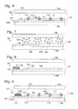
- FIG. 6 is a block diagram of an example of the display element of FIG. 2 , shown in a transparent state with coplanar electrodes and colorant particles compacted in recessed regions in accordance with an embodiment of the invention.
- FIG. 7 is a block diagram of the display element of FIG. 6 , shown in a colored state with colorant particles spread into a viewing area of the display system in accordance with an embodiment of the invention.
- FIG. 8 is a block diagram of the display element of FIG. 6 , shown in a transparent state with colorant particles adjacent one of the coplanar electrodes in accordance with an embodiment of the invention.
- FIG. 9 is a block diagram of an example of the display element of FIG. 2 , shown in a transparent state with coplanar electrodes, first colorant particles adjacent one of the coplanar electrodes, and second colorant particles compacted in recessed regions in accordance with an embodiment of the invention.
- FIG. 10 is a block diagram of the display element of FIG. 9 , shown in a colored state with the first colorant particles adjacent one of the coplanar electrodes and the second colorant particles spread into a viewing area of the display element in accordance with an embodiment of the invention.
- FIG. 11 is a block diagram of the display element of FIG. 9 , shown in a colored state with first and second colorant particles spread into the viewing area of the display system in accordance with an embodiment of the invention.
- FIG. 13 is a block diagram of the display element of FIG. 6 or FIG. 9 shown with coplanar electrodes and an opposed electrode in accordance with an embodiment of the invention.
- FIG. 14 is a block diagram of an example of the display element of FIG. 1 , shown with an example of a filter in accordance with an embodiment of the invention.
- FIG. 15 is a block diagram of the display element of FIG. 14 , shown with another example of a filter in accordance with an embodiment of the invention.
- FIG. 16 is a block diagram of the display element of FIG. 14 , shown with an example of a reflector in accordance with an embodiment of the invention.
- FIG. 17 is a block diagram of the display element of FIG. 14 , shown with another example of a reflector in accordance with an embodiment of the invention.
- FIG. 18 is a block diagram of the display element of FIG. 14 , shown with the filter of FIG. 14 and the reflector of FIG. 16 in accordance with an embodiment of the invention.
- FIG. 19 is a block diagram of the display element of FIG. 14 , shown with the filter of FIG. 14 and the reflector of FIG. 17 in accordance with an embodiment of the invention.
- FIG. 20 is a block diagram of the display element of FIG. 14 , shown with the filter of FIG. 15 and the reflector of FIG. 16 in accordance with an embodiment of the invention.
- FIG. 21 is a block diagram of the display element of FIG. 14 , shown with the filter of FIG. 15 and the reflector of FIG. 17 in accordance with an embodiment of the invention.
- FIG. 22 is a block diagram of an example of the display element of FIG. 4 or FIG. 5 , shown with filters and reflectors in accordance with an embodiment of the invention.
- FIG. 23 is a block diagram of the display element of FIG. 13 , shown with coplanar and opposed electrodes, a filter and a reflector in accordance with an embodiment of the invention.
- FIG. 1 shows an example of an electro-optical display system 30 having one or more display elements 32 .
- Display element 32 may be a segment, a pixel, a sub-pixel, or a super-pixel having two or more pixels.
- Display element 32 may include a display volume 34 , a source 36 and a sink 38 .
- Display volume 34 , source 36 and sink 38 may be fluidly connected and may contain a carrier fluid 40 having a plurality of colorant particles 42 .
- Source 36 may include colorant particles 42 that may be selectively controlled to enter display volume 34 .
- Sink 38 may receive colorant particles 42 from display volume 34 .
- the roles of source 36 and sink 38 may be reversed during operation of display element 32 . In other words, source 36 may become sink 38 , and vice-versa.
- Flow lines 44 may illustrate movement of colorant particles 42 from source 36 to sink 38 with convective movement of carrier fluid 40 .
- Colorant particles 42 may have any suitable size, such as between several nanometers and several microns. Additionally, colorant particles 42 may have the property of changing the spectral composition of the incident light by absorbing and/or scattering certain portions of the spectrum. As a result, colorant particles 42 may appear colored which provides a desired optical effect.
- Carrier fluid 40 may have colorant particles 42 with a single color or may have two or more sets of colorant particles 42 with each set having a different color from the other sets.
- display system 30 is shown to include colorant particles 42 , the display system may alternatively, or additionally, include one or more other suitable colorant technologies, such as dyed fluids, charged inks, oil films, etc.
- the convective currents illustrated by flow lines 44 of display element 32 may lead to any suitable movement of colorant particles 42 , such as out-of-plane movement (substantially transverse to substrate) as well as in-plane movement (substantially parallel to substrate), to provide the desired optical appearance.
- the convective currents may be generated in one or more suitable ways. For example, the convective currents may be generated by unbalanced volumetric forces inside the fluids that cause different parts of carrier fluid 40 to move relative to each other. Additionally, the convective currents may occur under gravity if different parts of carrier fluid 40 have different density caused, for example, by localized heating.
- convective currents may be generated by pressure or concentration gradients inside carrier fluid 40 produced by localized chemical reactions, localized heating or other disturbances. Furthermore, convective currents may occur if there are ionic currents in carrier fluid 40 caused by external electric fields (AC or DC) and there is charge injection into the carrier fluid. The moving ions may then create a pressure gradient through viscous drag and excluded volume effects.
- AC or DC external electric fields
- Such convective currents may sometimes be referred to as “electro-convective currents.”
- display system 30 may alternatively, or additionally, use any suitable physical principles to repel, attract, move, compress, concentrate or disperse colorants, such as electrokinetics, electrophoretics, electrowetting and electrofluidics.
- FIGS. 2-3 illustrate an example of a display element 48 for electro-optical display system 30 .
- display element 48 may include one or more components and/or one or more functions of the other display elements in this disclosure.
- Display element 48 may be a segment, a pixel, a sub-pixel, or a super-pixel having two or more pixels of electro-optical display system 30 .
- the layers of display element 48 shown in FIGS. 2-3 are for illustration only and may not represent the relative size or thickness of each layer.
- Display element 48 may include a plurality of electrodes 49 , such as a first electrode 50 and a second electrode 52 .
- First electrode 50 may be the conceptual “source” and may be made of transparent or opaque material(s)
- second electrode 52 may be the conceptual “sink” and may be made of transparent or opaque material(s).
- a dielectric layer 54 may be disposed, deposited or formed on second electrode 52 .
- Dielectric layer 54 may be transparent.
- dielectric layer 54 may include one or more colored dyes and/or one or more colorant particles.
- Dielectric layer 54 may include recessed regions 56 , which may be any suitable size(s) and/or shape(s). For example, recessed regions 56 may be sized to contain a plurality of colorant particles of display element 48 .
- dielectric layer 54 is shown to be formed on second electrode 52 , the dielectric layer may alternatively, or additionally, be formed on first electrode 50 .
- First electrode 50 may be fixed a distance apart from dielectric layer 54 and second electrode 52 to define a display volume 58 that holds a carrier fluid 60 having a plurality of colorant particles 62 .
- Carrier fluid 60 may include one or more polar fluids (e.g., water) and/or one or more non-polar fluids (e.g., dodecane). Additionally, or alternatively, carrier fluid 60 may include one or more anisotropic fluids, such as liquid crystal. Carrier fluid 60 also may include one or more surfactants (such as salts), charging agents, stabilizers, and dispersants. Carrier fluid 60 may include one or more dyed fluids, which may have a color different from the color of colorant particles 62 .
- First and second electrodes 50 , 52 may be configured to selectively move plurality of colorant particles 62 between a spread position S (as shown in FIG. 2 ) in which all or nearly all of the plurality of colorant particles may be out of recessed regions 56 and/or distributed or spread across display volume 58 to absorb and/or scatter incident light thereby creating a colored optical appearance (“colored state”), and a compacted position C (as shown in FIG. 3 ) in which all or nearly all of plurality of colorant particles 62 may be in recessed regions 56 thereby producing a clear optical appearance (“transparent state”).
- a spread position S as shown in FIG. 2
- a compacted position C as shown in FIG. 3
- first and second electrodes 50 , 52 may apply an electric potential difference, which may result in moving plurality of colorant particles 62 to compacted position C.
- Transverse solid lines of arrows in FIG. 3 may indicate electric field lines, while dashed lines of arrows leading into recessed regions 56 may indicate the flow of plurality of colorant particles 62 following the electrostatic and convective flows.
- the polarity of the voltage may be reversed. That reversal may induce convective flow in the opposite direction and colorant particles 62 may no longer be electrically contained in recessed regions 56 .
- plurality of colorant particles 62 may be mass transported to display volume 58 and then may spread relatively evenly throughout the display volume.
- the convective flow may be induced by ionic mass transport in carrier fluid 60 and charge transfer between the carrier fluid and the electrodes.
- the charge transfer may occur when carrier fluid 60 is coupled to the electrodes either through direct contact with the electrodes or separated from the electrodes by an intermediate layer comprising one or more materials. In the latter case, charge transfer may be facilitated by the internal electrical conductivity of the intermediate layer, either volumetric or via pinholes and other defects.
- the convective flow may be a transient effect caused by the ionic mass transport in carrier fluid 60 , but without charge transfer between the carrier fluid and the electrode.
- the convective flow may proceed for a finite amount of time and may facilitate the compaction of colorant particles 62 in recessed regions 56 . After that colorant particles 62 may be contained in recessed regions 56 by electrostatic forces generated by a coupling with the electrodes.
- Convection within display element 48 may also be induced by other means.
- convective flow can be induced by an electrokinetic means, a mechanical means (e.g., mechanical pistons), temperature gradients (e.g., heating of the sources and sinks, focused radiation), chemical potential gradients, as well as other means.
- FIG. 4 shows an example of a display element, which is generally indicated at 64 , having a dot structure for the recessed regions.
- display element 64 may include one or more components and/or one or more functions of the other display elements in this disclosure. Additionally, the layers of display element 64 shown in FIG. 4 are for illustration only and may not represent the relative size or thickness of each layer.
- FIG. 4 shows a top view 66 and a cross-sectional view 68 of display element 64 .
- Display element 64 may be a segment, a pixel, a sub-pixel, or a super-pixel having two or more pixels of electro-optical display system 30 .
- Display element 64 may include a display volume 69 defined by a first electrode 70 , a dielectric layer 72 having a plurality of recessed regions 74 , a second electrode 76 and a substrate 78 . As shown in FIG. 4 , recessed regions 74 may be shaped as dots and may be periodically distributed. Each dot-shaped recess region patterned into dielectric layer 72 may connect display volume 69 to second electrode 76 . Display element 64 also may include another substrate (not shown) on which first electrode 70 is disposed. Although recessed regions 74 are shown to be periodically distributed, the recessed regions may alternatively, or additionally, be aperiodically or stochastically distributed.
- FIG. 5 shows a top view 80 and a cross-sectional view 82 of a display element 84 having a dielectric layer with recessed regions that are in the form of lines or linear channels, which may be periodically or aperiodically distributed.
- display element 84 may include one or more components and/or one or more functions of the other display elements in this disclosure.
- the layers of display element 84 shown in FIG. 5 are for illustration only and may not represent the relative size or thickness of each layer.
- Display element 84 may include a first electrode 86 , a dielectric layer 88 having a plurality of recessed regions 90 , a second electrode 92 and a substrate 94 . Additionally, display element 84 may include another substrate (not shown) on which first electrode 86 is disposed.
- FIGS. 6-8 show another example of a display element, generally indicated at 134 , for electro-optical display system 30 .
- Display element 134 may be a segment, a pixel, a sub-pixel, or a super-pixel having two or more pixels of electro-optical display system 30 .
- display element 134 may include one or more components and/or one or more functions of the other display elements in this disclosure.
- the layers of the display element shown in FIGS. 6-8 are for illustration only and may not represent the relative size or thickness of each layer.
- Display element 134 may include a first substrate 136 , a second substrate 138 and a plurality of coplanar electrodes 140 .
- Plurality of coplanar electrodes 140 may include any suitable number of coplanar electrodes.
- plurality of coplanar electrodes 140 may include a first coplanar electrode 142 and a second coplanar electrode 144 .
- coplanar electrodes 140 may be any suitable size(s).
- first coplanar electrode 142 may be smaller than second coplanar electrode 144 , or vice-versa.
- a dielectric layer 146 having recessed regions 148 may be disposed on at least one of coplanar electrodes 140 .
- dielectric layer 146 may be disposed or formed on second coplanar electrode 144 .
- First substrate 136 , the coplanar electrodes and dielectric layer 146 may define a display volume 150 that holds or contains a carrier fluid 152 having a plurality of colorant particles 154 .
- Carrier fluid 152 may be a clear or dyed fluid, and plurality of colorant particles 154 may be any suitable color.
- colorant particles 154 shown in FIGS. 6-8 are for illustration only and may not reflect the actual number of colorant particles in display element 134 or the size of the colorant particles relative to each other or to the layers of the display element.
- Coplanar electrodes 140 may be configured to selectively move plurality of colorant particles 154 between compacted position C (as shown in FIG. 6 ) in which all or nearly all of the plurality of colorant particles may be in recessed regions 148 , and spread position S (as shown in FIG. 7 ) in which all or nearly all of the plurality of colorant particles may be out of the recessed regions and/or distributed or spread across display volume 150 relative to the compacted position (and collected position as described below).
- first electrode 142 may have a negative polarity and second electrode 144 may have a positive polarity to move colorant particles 154 to compacted position C.
- first and second electrodes 142 , 144 may provide the opposite bias (such as a positive bias for the first electrode and/or a negative bias for the second electrode), a pulsed bias and/or a pulsed waveform.
- Coplanar electrodes 140 may additionally be configured to move plurality of colorant particles 154 to a collected position A (as shown in FIG. 8 ) in which all or nearly all of the plurality of colorant particles may be collected adjacent one of the coplanar electrodes, such as first coplanar electrode 142 , and spaced from the other coplanar electrodes, such as second coplanar electrode 144 .
- first coplanar electrode 142 may have a positive polarity
- second coplanar electrode 144 may have a negative polarity to move colorant particles 154 to collected position A.
- Colorant particles 154 may alternatively be positively charged and the polarities discussed above may be reversed to move those particles accordingly.
- Display element 134 may include a backplane 155 , as shown in FIG. 6 , which may include plurality of coplanar electrodes 140 and/or second substrate 138 .
- FIGS. 9-12 show another example of a display element, generally indicated at 156 , for electro-optical display system 30 .
- Display element 156 may be a segment, a pixel, a sub-pixel, or a super-pixel having two or more pixels of electro-optical display system 30 .
- display element 156 may include one or more components and/or one or more functions of the other display elements in this disclosure.
- the layers of display element 156 shown in FIGS. 9-12 are for illustration only and may not represent the relative size or thickness of each layer.
- the colorant particles shown in FIGS. 9-12 are for illustration only and may not reflect the actual number of colorant particles in the display element or the size of the colorant particles relative to each other or to the layers of display element 156 .
- Display element 156 may include a first substrate 158 , a second substrate 160 and a plurality of coplanar electrodes 162 .
- Plurality of coplanar electrodes 162 may include any suitable number of coplanar electrodes.
- plurality of coplanar electrodes 162 may include a first coplanar electrode 164 and a second coplanar electrode 166 .
- coplanar electrodes 162 may be any suitable size(s).
- first coplanar electrode 164 may be smaller than second coplanar electrode 166 , or vice-versa.
- a dielectric layer 168 having recessed regions 170 may be disposed on at least one of coplanar electrodes 162 .
- dielectric layer 168 may be disposed or formed on second electrode 166 .
- First substrate 158 , coplanar electrodes 162 and dielectric layer 168 may define a display volume 172 that holds or contains a carrier fluid 174 having a plurality of colorant particles 176 .
- Carrier fluid 174 may be a clear or dyed fluid.
- Plurality of colorant particles 176 may include first colorant particles 178 having a first color, and second colorant particles 180 having a second color different from the first color.
- the first and second colors may be any suitable colors, such as black and magenta, magenta and cyan, cyan and yellow, green and magenta, or any other suitable combinations, including combinations of red, green, blue, cyan, magenta, yellow, white and/or spot color(s).
- Coplanar electrodes 162 may be configured to selectively move plurality of colorant particles 176 among a first compacted position C 1 (as shown in FIG. 9 ) in which all or nearly all of first colorant particles 178 may be adjacent first electrode 164 and all or nearly all of second colorant particles 180 may be in recessed regions 170 , a first spread position S 1 (as shown in FIG. 10 ) in which all or nearly all of the second colorant particles may be out of the recessed regions and/or all or nearly all of the second colorant particles may be distributed or spread across display volume 172 relative to the first compacted position (and the second compacted position as described below), and a second spread position S 2 (as shown in FIG.
- first electrode 164 may have a negative polarity and second electrode 166 may have a positive polarity to move colorant particles 176 to first compacted position C 1 .
- first and second electrodes 164 , 166 may provide the opposite bias (such as a positive bias for the first electrode and/or a negative bias for the second electrode), a pulsed bias and/or a pulsed waveform.
- Asymmetric travel distances for first and second colorant particles 178 , 180 may be used for independent control of those particles.
- the colorant particles adjacent to the smaller electrode may respond slower to an applied bias due to travel distance of those particles from the smaller electrode to display volume 172 .
- First and second colorant particles 178 , 180 may thus move to first spread position S 1 , as shown in FIG. 10 , on an initial application of a bias, and then may move to second spread position S 2 , as shown in FIG. 11 , on a continued or second application of a bias.
- Coplanar electrodes 162 may additionally be configured to move plurality of colorant particles 176 to a second compacted position C 2 in which all or nearly all of second colorant particles 180 may be adjacent first electrode 164 and all or nearly all of the first colorant particles may be in recessed regions 170 (as shown in FIG. 12 ).
- first colorant particles 178 are positively charged and second colorant particles 180 are negatively charged
- first electrode 164 may have a positive polarity
- second electrode 166 may have a negative polarity to move colorant particles 176 to second compacted position C 2 .
- First and second colorant particles 178 , 180 may alternatively be negatively and positively charged, respectively, and the polarities discussed above may be reversed to move those particles accordingly.
- Display element 156 may include a backplane 181 , as shown in FIG. 9 , which may additionally include plurality of coplanar electrodes 162 and/or second substrate 160 .
- colorant particles 176 are shown to include particles of two different colors, the colorant particles may alternatively include particles of three, four, five or more different colors.
- Display element 156 may include additional structure discussed in this disclosure.
- the display element may include one or more electrodes that are not within the same plane as the coplanar electrodes, such as at least one opposed electrode 181 , as shown in FIG. 13 .
- Opposed electrode 181 and coplanar electrodes 162 may be configured to move all or nearly all of the colorant particles out of and/or into the recessed regions, such as rate(s) faster than with only the coplanar electrodes.
- opposed electrode 181 may serve as a reference electrode to build up potential between coplanar electrodes 162 .
- FIGS. 14-21 show examples of a display element for electro-optical display system 30 , generally indicated at 182 .
- Display element 182 may be a segment, a pixel, a sub-pixel, or a super-pixel having two or more pixels of electro-optical display system 30 .
- display element 182 may include one or more components and/or one or more functions of the other display elements in this disclosure.
- the layers of display element 182 shown in FIGS. 14-21 are for illustration only and may not represent the relative size or thickness of each layer.
- Display element 182 may include a display volume 184 and one or more color elements 185 , which may include any suitable structure configured to modulate at least one wavelength of light.
- color elements 185 may include one or more filters 186 and/or one or more reflectors 188 .
- display element 182 may include other components, such as electrodes, substrates, colorant particles, fluids, dielectric layers, etc., those components are not shown to primarily illustrate the different combinations of colorant particles, filters and/or reflectors that may be used with a display element for an electro-optical display system that may be used to create various color embodiments.
- Display element 182 may include a single filter 186 , generally indicated at 190 in FIG. 14 .
- Filter 190 may be any suitable color, such as red, green, blue, cyan, magenta, yellow, white, spot color(s) (color(s) matched to specific application(s)), a color different from the color of the colorant particles and/or fluid, and/or other suitable color(s).
- display element 182 may include a plurality of filters 192 (also may be referred to as a “segmented filter” or “pixelated filter”), as shown in FIG. 15 .
- Those filters may be any suitable colors, such as red, blue, green, cyan, magenta, yellow and/or white filters.
- Display element 182 also may include a single reflector 188 , generally indicated at 194 in FIG. 16 .
- Reflector 194 may be configured to reflect at least one wavelength of light.
- reflector 194 may be configured to reflect the wavelengths of light corresponding to the color white (may be referred to as a “white reflector”).
- reflector 194 may be configured to reflect the wavelengths of light corresponding to the color red, blue, green (“a red reflector,” “a blue reflector” and “a green reflector,” respectively), cyan, magenta, yellow, white, spot color(s) and/or other suitable color(s).
- display element 182 may include a plurality of reflectors 196 (also may be referred to as a “segmented reflector” or “pixelated reflector”), as shown in FIG. 17 .
- Reflectors 196 may be any suitable colors, such as one or more of the colors discussed above for reflector 194 .
- Display element 182 may be configured with different transparent and colored states by using different colorant particles, different filters and/or different reflectors. For example, display element 182 may switch between a spot color and a white color by using colorant particles having the spot color and a white reflector 194 (or segmented white reflector 196 ). Additionally, display element 182 may switch between first and second colors by using colorant particles with a third color (where the third color combined with the first color results in the second color) and reflector 194 (or segmented reflector 196 ) configured to reflect the first color. Moreover, display element 182 may provide full color by various color reflectors 196 , such as reflectors that reflect the color red, green, blue, white, cyan, magenta, yellow, and/or spot color(s).
- various color reflectors 196 such as reflectors that reflect the color red, green, blue, white, cyan, magenta, yellow, and/or spot color(s).
- Display element 182 may alternatively include both filter 186 and reflector 188 .
- display element 182 may include filter 190 and reflector 194 , as shown in FIG. 18 .
- display element 182 may include filter 190 and segmented reflector 196 , as shown in FIG. 19 .
- Display element 182 such as shown in FIG. 18 or 19 , may be configured with different transparent and colored states by using different colorant particles, different filters and/or different reflectors.
- display element 182 may switch between a spot color and a black color by using a spot color filter 190 and a white reflector 194 (or segmented white reflector 196 ) with black colorant particles.
- display element 182 may switch between first and second colors by using a filter 190 with the first color, colorant particles with a third color (where the third color combined with the first color results in the second color), and a white reflector 194 (or segmented white reflector 196 ).
- Display element 182 may alternatively include segmented filter 192 with reflector 194 , as shown in FIG. 20 .
- display element 182 may include segmented filter 192 and segmented reflector 196 , as shown in FIG. 21 .
- Display element 182 such as shown in FIGS. 20-21 , may be configured with different transparent and colored states by using different colorant particles, different filters and/or different reflectors.
- display element 182 may provide full color by using various color filters 192 , such as red, green, blue and white filters, and a white reflector 194 (or segmented white reflector 196 ). Further variations of the above also are possible by using a transparent dielectric layer, a dyed dielectric layer or a dielectric layer with colorant particles.
- Display element 286 may be a segment, a pixel, a sub-pixel, or a super-pixel having two or more pixels of electro-optical display system 30 .
- display element 286 may include one or more components and/or one or more functions of the other display elements in this disclosure.
- the layers of display element 286 shown in FIG. 22 are for illustration only and may not represent the relative size or thickness of each layer.
- the colorant particles shown in FIG. 22 are for illustration only and may not reflect the actual number of colorant particles in the display element or the size of the colorant particles relative to each other or to the layers of the display element.
- Display element 286 includes a first substrate 288 , a plurality of electrodes 290 , a dielectric layer 292 having recessed regions 294 , and a second substrate 296 .
- Plurality of electrodes 290 includes a first opposed electrode 297 and coplanar electrodes 298 .
- Plurality of electrodes 290 and dielectric layer 292 defines a display volume 300 that holds or contains a carrier fluid 302 having a plurality of colorant particles 304 .
- Coplanar electrodes 290 include pixel plate electrodes. Those electrodes may sometimes be referred to as a segmented or pixelated second electrode 298 .
- segmented second electrode 298 includes a first segment 306 , a second segment 308 and a third segment 310 . Those segments are electrically disconnected such that each segment has a different electrical polarity than an adjacent segment.
- plurality of colorant particles 304 may be negatively charged and may include a first portion 312 , a second portion 314 and a third portion 316 .
- First and third segments 306 , 310 may be negatively charged to move first and third portions 312 , 316 of colorant particles 304 to the spread position, while second segment 308 may be positively charged to move second portion 314 of the colorant particles to the compacted position, as shown in FIG. 22 .
- Segmented second electrode 298 includes at least one reflector or reflector layer 318 .
- Reflector layer 318 is configured to reflect at least one wavelength of light, such as when plurality of colorant particles 304 are in recessed regions 294 and/or display element 286 is in the transparent or clear state.
- reflector layer 318 may include a white reflector layer that is configured to reflect the wavelengths of light corresponding to the color white.
- reflector layer 318 may include one or more non-white reflector layers that may be configured to reflect the wavelengths of light corresponding to the color red, blue, green, cyan, magenta, yellow, white, spot color(s) and/or other suitable color(s).
- first segment 306 includes a first reflector layer 320
- second segment 308 includes a second reflector layer 322
- third segment 310 includes a third reflector layer 324 .
- First, second and/or third reflector layers 320 , 322 , 324 are configured to reflect wavelengths of light corresponding to the same or different colors.
- each of those reflector layers may be configured to reflect wavelengths of light corresponding to any suitable color, such as the color white.
- first, second, and third reflector layers 320 , 322 , 324 may be configured to reflect wavelengths of light corresponding to the colors red, blue and green.
- Display element 286 includes a backplane 325 (such as an active matrix backplane) that includes coplanar electrodes (or segmented second electrode) 298 and/or second substrate 296 .
- first electrode 297 may alternatively, or additionally, be segmented or pixelated.
- second electrode 298 is shown to include three segments, the second electrode may include any suitable number of segments, such as two, four, five, six, seven, etc.
- segmented second electrode 298 may include four or more segments each with a reflector layer configured to reflect wavelengths of light corresponding to the colors red, blue, green or white.
- colorant particles 304 are discussed to be negatively charged, those particles may be positively charged.
- a single recess region is shown above each segment, there may be two or more recess regions per segment.
- segmented second electrode 298 is shown to include a reflector layer, first electrode 297 and/or dielectric layer 292 may alternatively include or incorporate the reflector layer.
- Display element 286 also includes at least one filter 326 , which may include any suitable structure configured to absorb at least one wavelength of light.
- Filter 326 is formed or incorporated on top of the first substrate and/or between the first substrate and the first electrode.
- Filter 326 may be a color filter of any suitable color(s), such as red, blue, green, white, cyan, magenta, yellow, any suitable spot color(s) and/or any other color(s).
- Display element 286 may include, for example, a first filter 328 , a second filter 330 and a third filter 332 , as shown in FIG. 22 .
- Those filters may be any suitable size(s).
- Each filter may include a different color, such as red, blue and green.
- display element 286 may include a color filter for each electrode, such as shown in FIG. 22 for each segment of segmented second electrode 298 .
- Reflector 318 and filter 326 may be generally referred to as color elements of display element 286 .
- display element 286 is shown to include three filters, the display element may include any suitable number of filters, such as one, two, four, five or more filters. Additionally, although display element 286 is shown to include red, blue and green filters, those filters may include any suitable color(s), such as cyan, magenta, yellow, white, spot color(s), color(s) different from the color of the colorant particles, and/or red, blue, green and white colors. Moreover, although display element 286 is shown to include a filter for each segmented electrode, there may be more than one filter for each segmented electrode or more than one segmented electrode for each filter. For example, display element 286 may include a single color filter of any suitable color.
- Display element 356 may be a segment, a pixel, a sub-pixel, or a super-pixel having two or more pixels of electro-optical display system 30 .
- display element 356 may include one or more components and/or one or more functions of the other display elements in this disclosure. Additionally, the layers of display element 356 shown in FIG. 23 are for illustration only and may not represent the relative size or thickness of each layer.
- Display element 356 may include a first substrate 358 , a second substrate 360 and a plurality of coplanar electrodes 362 .
- Plurality of coplanar electrodes 362 may include any suitable number of coplanar electrodes.
- plurality of coplanar electrodes 362 may include a first coplanar electrode 364 and a second coplanar electrode 366 .
- coplanar electrodes 362 may be any suitable size(s).
- first coplanar electrode 364 may be smaller than second coplanar electrode 366 , or vice-versa.
- a dielectric layer 368 having recessed regions 370 may be disposed or formed on at least one of coplanar electrodes 362 .
- dielectric layer 368 may be disposed or formed on second electrode 366 .
- display element 356 may include at least one opposed electrode 382 .
- display element 356 may include at least one color filter 384 and/or at least one reflector layer 386 , as shown in FIG. 23 .
- Filter 384 may be any suitable color(s), and reflector layer 386 may reflect any suitable color(s).
- the display elements may alternatively, or additionally, include electrokinetic elements, heating elements, microfluidic elements, micro-electromechanical elements, etc.
Abstract
Description
Claims (20)
Priority Applications (1)
| Application Number | Priority Date | Filing Date | Title |
|---|---|---|---|
| US12/643,742 US8089687B2 (en) | 2009-12-21 | 2009-12-21 | Electro-optical display systems |
Applications Claiming Priority (1)
| Application Number | Priority Date | Filing Date | Title |
|---|---|---|---|
| US12/643,742 US8089687B2 (en) | 2009-12-21 | 2009-12-21 | Electro-optical display systems |
Publications (2)
| Publication Number | Publication Date |
|---|---|
| US20110149376A1 US20110149376A1 (en) | 2011-06-23 |
| US8089687B2 true US8089687B2 (en) | 2012-01-03 |
Family
ID=44150676
Family Applications (1)
| Application Number | Title | Priority Date | Filing Date |
|---|---|---|---|
| US12/643,742 Expired - Fee Related US8089687B2 (en) | 2009-12-21 | 2009-12-21 | Electro-optical display systems |
Country Status (1)
| Country | Link |
|---|---|
| US (1) | US8089687B2 (en) |
Cited By (9)
| Publication number | Priority date | Publication date | Assignee | Title |
|---|---|---|---|---|
| US20110248909A1 (en) * | 2010-04-12 | 2011-10-13 | Seiko Epson Corporation | Electrophoretic display device and electronic apparatus |
| US20110304529A1 (en) * | 2010-06-15 | 2011-12-15 | Jong-Souk Yeo | Display element |
| US20130033740A1 (en) * | 2011-08-01 | 2013-02-07 | Hong Seok-Joon | Electrophoretic Display Device |
| WO2013181649A1 (en) * | 2012-06-01 | 2013-12-05 | E Ink Corporation | Methods for driving electro-optic displays |
| US8698734B2 (en) | 2010-04-12 | 2014-04-15 | Seiko Epson Corporation | Electrophoretic display device, driving method of the same, and electronic apparatus |
| US10282033B2 (en) | 2012-06-01 | 2019-05-07 | E Ink Corporation | Methods for updating electro-optic displays when drawing or writing on the display |
| US11708720B2 (en) | 2013-10-22 | 2023-07-25 | E Ink Corporation | Light-modulating electrophoretic device |
| US11733557B2 (en) | 2013-03-22 | 2023-08-22 | E Ink Corporation | Electrophoretic device having a transparent light state |
| US11762258B2 (en) | 2019-09-30 | 2023-09-19 | E Ink Corporation | Electrically-actuated variable transmission film having very low haze and a visible grid in a clear state |
Families Citing this family (5)
| Publication number | Priority date | Publication date | Assignee | Title |
|---|---|---|---|---|
| KR101495414B1 (en) * | 2010-06-02 | 2015-02-24 | 이 잉크 코포레이션 | Color electro-optic displays |
| US8179590B1 (en) * | 2010-11-22 | 2012-05-15 | Hewlett-Packard Development Company, L.P. | Electro-optical display |
| JP2015096873A (en) * | 2012-02-28 | 2015-05-21 | シャープ株式会社 | Display panel and display device |
| GB201506147D0 (en) | 2015-04-10 | 2015-05-27 | Hanna Moore & Curley | A Micro-Fastened, Sealed Light Modulator |
| JP2022517262A (en) * | 2019-01-16 | 2022-03-07 | クラウン エレクトロキネティクス コーポレイション | Application of electrokinetic devices for imaging systems |
Citations (129)
| Publication number | Priority date | Publication date | Assignee | Title |
|---|---|---|---|---|
| US3668106A (en) | 1970-04-09 | 1972-06-06 | Matsushita Electric Ind Co Ltd | Electrophoretic display device |
| US3806893A (en) | 1971-07-29 | 1974-04-23 | Matsushita Electric Ind Co Ltd | Method of electrically detecting colloidal memory |
| US3850627A (en) | 1971-01-06 | 1974-11-26 | Xerox Corp | Electrophoretic imaging method |
| US3892568A (en) | 1969-04-23 | 1975-07-01 | Matsushita Electric Ind Co Ltd | Electrophoretic image reproduction process |
| US4041481A (en) | 1974-10-05 | 1977-08-09 | Matsushita Electric Industrial Co., Ltd. | Scanning apparatus for an electrophoretic matrix display panel |
| US4045327A (en) | 1974-08-28 | 1977-08-30 | Matsushita Electric Industrial Co., Ltd. | Electrophoretic matrix panel |
| US4068927A (en) | 1976-09-01 | 1978-01-17 | North American Philips Corporation | Electrophoresis display with buried lead lines |
| US4071430A (en) | 1976-12-06 | 1978-01-31 | North American Philips Corporation | Electrophoretic image display having an improved switching time |
| US4088395A (en) | 1976-05-27 | 1978-05-09 | American Cyanamid Company | Paper counter-electrode for electrochromic devices |
| US4123346A (en) | 1976-05-11 | 1978-10-31 | Thomson-Csf | Electrophoretic device |
| US4126854A (en) | 1976-05-05 | 1978-11-21 | Xerox Corporation | Twisting ball panel display |
| US4149149A (en) | 1976-02-20 | 1979-04-10 | Hitachi, Ltd. | Circuit for actuating a display with an improved comparator |
| US4203106A (en) | 1977-11-23 | 1980-05-13 | North American Philips Corporation | X-Y addressable electrophoretic display device with control electrode |
| JPS5596922A (en) | 1979-01-19 | 1980-07-23 | Sharp Corp | Liquid crystal display element |
| US4218302A (en) | 1979-08-02 | 1980-08-19 | U.S. Philips Corporation | Electrophoretic display devices |
| US4305807A (en) | 1980-03-13 | 1981-12-15 | Burroughs Corporation | Electrophoretic display device using a liquid crystal as a threshold device |
| US4408202A (en) | 1979-11-13 | 1983-10-04 | Fales John D | Electrokinetic display system |
| US4418346A (en) | 1981-05-20 | 1983-11-29 | Batchelder J Samuel | Method and apparatus for providing a dielectrophoretic display of visual information |
| US4430648A (en) | 1980-01-22 | 1984-02-07 | Citizen Watch Company Limited | Combination matrix array display and memory system |
| US4450440A (en) | 1981-12-24 | 1984-05-22 | U.S. Philips Corporation | Construction of an epid bar graph |
| US4522472A (en) | 1982-02-19 | 1985-06-11 | North American Philips Corporation | Electrophoretic image display with reduced drives and leads |
| US4648956A (en) | 1984-12-31 | 1987-03-10 | North American Philips Corporation | Electrode configurations for an electrophoretic display device |
| JPS6258222A (en) | 1985-09-09 | 1987-03-13 | Ricoh Co Ltd | Matrix type display device |
| US4726662A (en) | 1985-09-24 | 1988-02-23 | Talig Corporation | Display including a prismatic lens system or a prismatic reflective system |
| US4732456A (en) | 1984-08-28 | 1988-03-22 | Taliq Corporation | Scattering display for contrast enhancement including target |
| US4741604A (en) | 1985-02-01 | 1988-05-03 | Kornfeld Cary D | Electrode arrays for cellular displays |
| US4772102A (en) | 1987-05-18 | 1988-09-20 | Taliq Corporation | Display with light traps between reflector and scattering means |
| US4824208A (en) | 1984-08-28 | 1989-04-25 | Talig Corporation | Display for contrast enhancement |
| US4832458A (en) | 1984-08-28 | 1989-05-23 | Talig Corporation | Display for contrast enhancement |
| EP0361420A2 (en) | 1988-09-28 | 1990-04-04 | Ube Industries, Ltd. | Liquid crystal display device |
| EP0404545A2 (en) | 1989-06-20 | 1990-12-27 | Japan Synthetic Rubber Co., Ltd. | Active matrix substrate for liquid crystal display device |
| EP0443571A2 (en) | 1990-02-23 | 1991-08-28 | Ube Industries, Ltd. | Liquid crystal display panel |
| US5057244A (en) | 1983-10-20 | 1991-10-15 | Ricoh Company, Ltd. | Transparent, electrically conductive film |
| US5105185A (en) | 1989-07-12 | 1992-04-14 | Alps Electric Co., Ltd. | Display method, device for realizing same and displaying medium used therefor |
| EP0186710B1 (en) | 1984-06-18 | 1992-10-07 | Nissha Printing Co., Ltd. | Liquid-crystal multi-color display device |
| WO1992017873A1 (en) | 1991-03-27 | 1992-10-15 | Copytele, Inc. | Electrophoretic display panel with semiconductor coated elements |
| WO1992020060A1 (en) | 1991-05-06 | 1992-11-12 | Copytele, Inc. | Electrophoretic display panel with tapered grid insulators and associated methods |
| WO1992021733A1 (en) | 1991-05-30 | 1992-12-10 | Copytele, Inc. | Methods of fabricating dual anode, flat panel electrophoretic displays |
| WO1993002443A1 (en) | 1991-07-15 | 1993-02-04 | Copytele, Inc. | Electrophoretic display employing grey scale capability utilizing area modulation |
| WO1993004458A1 (en) | 1991-08-23 | 1993-03-04 | Copytele, Inc. | Electrophoretic display with single character erasure |
| WO1993004459A1 (en) | 1991-08-19 | 1993-03-04 | Copytele, Inc. | Electrophoretic display panel with interleaved local anode |
| WO1993005425A1 (en) | 1991-08-29 | 1993-03-18 | Copytele, Inc. | Electrophoretic display panel with internal mesh background screen |
| WO1993007608A1 (en) | 1991-10-07 | 1993-04-15 | Copytele, Inc. | Electrode structure for an electrophoretic display apparatus |
| US5223823A (en) | 1991-03-11 | 1993-06-29 | Copytele, Inc. | Electrophoretic display panel with plural electrically independent anode elements |
| WO1993017414A1 (en) | 1992-02-25 | 1993-09-02 | Copytele, Inc. | Electrophoretic display panel and associated methods providing single pixel erase capability |
| US5250932A (en) | 1988-04-13 | 1993-10-05 | Ube Industries, Ltd. | Liquid crystal display device |
| US5250938A (en) | 1990-12-19 | 1993-10-05 | Copytele, Inc. | Electrophoretic display panel having enhanced operation |
| US5254981A (en) | 1989-09-15 | 1993-10-19 | Copytele, Inc. | Electrophoretic display employing gray scale capability utilizing area modulation |
| US5302235A (en) | 1989-05-01 | 1994-04-12 | Copytele, Inc. | Dual anode flat panel electrophoretic display apparatus |
| US5315312A (en) | 1991-05-06 | 1994-05-24 | Copytele, Inc. | Electrophoretic display panel with tapered grid insulators and associated methods |
| US5345251A (en) | 1993-01-11 | 1994-09-06 | Copytele, Inc. | Electrophoretic display panel with interleaved cathode and anode |
| US5359346A (en) | 1992-02-25 | 1994-10-25 | Copytele, Inc. | Electrophoretic display panel and associated methods for blinking displayed characters |
| US5389945A (en) | 1989-11-08 | 1995-02-14 | Xerox Corporation | Writing system including paper-like digitally addressed media and addressing device therefor |
| WO1995006307A1 (en) | 1993-08-26 | 1995-03-02 | Copytele, Inc. | Electrophoretic display having reduced writing time |
| WO1995007527A1 (en) | 1993-09-09 | 1995-03-16 | Copytele, Inc. | Electrophoretic display panel with selective character addressability |
| US5402145A (en) | 1993-02-17 | 1995-03-28 | Copytele, Inc. | Electrophoretic display panel with arc driven individual pixels |
| WO1995010107A1 (en) | 1993-10-01 | 1995-04-13 | Copytele, Inc. | Electrophoretic display panel with selective character addressability |
| US5412398A (en) | 1992-02-25 | 1995-05-02 | Copytele, Inc. | Electrophoretic display panel and associated methods for blinking displayed characters |
| EP0684579A2 (en) | 1994-05-23 | 1995-11-29 | International Business Machines Corporation | Touchpad |
| DE4431441C1 (en) | 1994-09-03 | 1996-02-15 | Licentia Gmbh | Communication circuitry with remotely located system having sensors and control devices |
| US5499038A (en) | 1991-11-21 | 1996-03-12 | Copytele, Inc. | Method of operation for reducing power, increasing life and improving performance of EPIDs |
| EP0525852B1 (en) | 1991-07-09 | 1996-05-22 | Koninklijke Philips Electronics N.V. | Display device |
| DE19500694A1 (en) | 1995-01-12 | 1996-08-08 | Martin Hauck | HF image reproduction device |
| US5565885A (en) | 1990-05-16 | 1996-10-15 | Kabushiki Kaisha Toshiba | Liquid crystal display panel and liquid crystal display device |
| US5575554A (en) | 1991-05-13 | 1996-11-19 | Guritz; Steven P. W. | Multipurpose optical display for articulating surfaces |
| GB2306229A (en) | 1995-10-13 | 1997-04-30 | Ibm | Diffusely reflective display cell |
| US5684501A (en) | 1994-03-18 | 1997-11-04 | U.S. Philips Corporation | Active matrix display device and method of driving such |
| US5717515A (en) | 1995-12-15 | 1998-02-10 | Xerox Corporation | Canted electric fields for addressing a twisting ball display |
| US5729663A (en) | 1995-12-07 | 1998-03-17 | Xerox Corporation | Method and apparatus for gray screening |
| US5739801A (en) | 1995-12-15 | 1998-04-14 | Xerox Corporation | Multithreshold addressing of a twisting ball display |
| US5745094A (en) | 1994-12-28 | 1998-04-28 | International Business Machines Corporation | Electrophoretic display |
| JPH10149118A (en) | 1996-11-21 | 1998-06-02 | Nok Corp | Electrophoresis display device |
| US5786875A (en) | 1996-03-15 | 1998-07-28 | Brader; Lawrence Allen | Thermal liquid crystal display using thermoelectric link |
| US6130774A (en) | 1998-04-27 | 2000-10-10 | E Ink Corporation | Shutter mode microencapsulated electrophoretic display |
| US6177921B1 (en) | 1997-08-28 | 2001-01-23 | E Ink Corporation | Printable electrode structures for displays |
| US6225971B1 (en) | 1998-09-16 | 2001-05-01 | International Business Machines Corporation | Reflective electrophoretic display with laterally adjacent color cells using an absorbing panel |
| US6271823B1 (en) | 1998-09-16 | 2001-08-07 | International Business Machines Corporation | Reflective electrophoretic display with laterally adjacent color cells using a reflective panel |
| US6323989B1 (en) | 1996-07-19 | 2001-11-27 | E Ink Corporation | Electrophoretic displays using nanoparticles |
| US20030013238A1 (en) | 2000-10-11 | 2003-01-16 | Canon Kabushiki Kaisha | Display device and manufacturing method therefor |
| US6574034B1 (en) | 2002-01-16 | 2003-06-03 | Xerox Corporation | Electrophoretic displays, display fluids for use therein, and methods of displaying images |
| US6577433B1 (en) | 2002-01-16 | 2003-06-10 | Xerox Corporation | Electrophoretic displays, display fluids for use therein, and methods of displaying images |
| US6639580B1 (en) | 1999-11-08 | 2003-10-28 | Canon Kabushiki Kaisha | Electrophoretic display device and method for addressing display device |
| US6710540B1 (en) | 1995-07-20 | 2004-03-23 | E Ink Corporation | Electrostatically-addressable electrophoretic display |
| US6741385B2 (en) | 2001-06-26 | 2004-05-25 | Canon Kabushiki Kaisha | Electrophoretic display device |
| US6781745B2 (en) | 2001-09-12 | 2004-08-24 | Sipix Imaging, Inc. | Electrophoretic display with gating electrodes |
| US6806995B2 (en) | 2001-10-29 | 2004-10-19 | Sipix Imaging, Inc. | Electrophoretic display with holding electrodes |
| US6822783B2 (en) | 2001-06-26 | 2004-11-23 | Canon Kabushiki Kaisha | Electrophoretic display unit, and driving method thereof |
| US20050052402A1 (en) | 2001-11-21 | 2005-03-10 | Hajime Kitano | Reversible image display sheet and image display |
| US6897996B2 (en) | 2001-09-12 | 2005-05-24 | Canon Kabushiki Kaisha | Electrophoretic display device |
| WO2005093508A1 (en) | 2004-03-23 | 2005-10-06 | Koninklijke Philips Electronics N.V. | Electrophoretic display panel |
| US6967763B2 (en) | 2003-03-11 | 2005-11-22 | Fuji Photo Film Co., Ltd. | Display device |
| US20050266590A1 (en) | 2004-05-28 | 2005-12-01 | Nam-Seok Roh | Electrophoretic display device |
| US20050285816A1 (en) | 1999-02-26 | 2005-12-29 | Micron Technology, Inc. | Electrowetting display |
| WO2006016302A2 (en) | 2004-08-10 | 2006-02-16 | Koninklijke Philips Electronics N.V. | Electrophoretic color display panel |
| US7034987B2 (en) | 2002-02-19 | 2006-04-25 | Koninklijke Philips Electronics N.V. | Electrophoretic display device |
| US20060087489A1 (en) | 2002-07-17 | 2006-04-27 | Ryou Sakurai | Image display |
| US7038656B2 (en) | 2002-08-16 | 2006-05-02 | Sipix Imaging, Inc. | Electrophoretic display with dual-mode switching |
| US7053882B2 (en) | 2003-07-21 | 2006-05-30 | Er Display Limited | Display apparatus |
| EP1370904B1 (en) | 2001-03-14 | 2006-07-05 | Koninklijke Philips Electronics N.V. | Electrophoretic display device |
| US7116466B2 (en) | 2004-07-27 | 2006-10-03 | E Ink Corporation | Electro-optic displays |
| US7123238B2 (en) | 2002-01-16 | 2006-10-17 | Xerox Corporation | Spacer layer for electrophoretic display device |
| US20070075941A1 (en) | 2003-10-08 | 2007-04-05 | Koninklijke Philips Electronics N.V. | Electrowetting display device |
| WO2007042950A2 (en) | 2005-10-14 | 2007-04-19 | Koninklijke Philips Electronics N.V. | In-plane switching display devices |
| US20070103428A1 (en) | 2005-11-04 | 2007-05-10 | Xerox Corporation | Display device |
| US20070109622A1 (en) | 2003-09-30 | 2007-05-17 | Canon Kabushiki Kaisha | Display apparatus |
| US7230751B2 (en) | 2005-01-26 | 2007-06-12 | E Ink Corporation | Electrophoretic displays using gaseous fluids |
| US20070205979A1 (en) | 2006-03-02 | 2007-09-06 | Bigelow Donald O | Electro-optical modulating display devices comprising and array of microcells and a method for making such devices |
| US7277219B2 (en) | 2004-12-07 | 2007-10-02 | Canon Kabushiki Kaisha | Particle movement-type display device and particle movement-type display apparatus |
| EP1714186B1 (en) | 2004-02-06 | 2007-11-14 | Koninklijke Philips Electronics N.V. | Electrophoretic display panel |
| US20070268560A1 (en) | 2006-05-19 | 2007-11-22 | Xerox Corporation | Electrophoretic display device and method of displaying image |
| WO2008007300A1 (en) | 2006-07-11 | 2008-01-17 | Koninklijke Philips Electronics N.V. | An improved electrode layout for a display |
| US7352353B2 (en) | 1995-07-20 | 2008-04-01 | E Ink Corporation | Electrostatically addressable electrophoretic display |
| US7365732B2 (en) | 2002-05-13 | 2008-04-29 | Canon Kabushiki Kaisha | Display device employing electrophoretic migration |
| US20080100906A1 (en) | 2006-10-30 | 2008-05-01 | Xerox Corporation | Color display device |
| US20080117165A1 (en) | 2006-11-17 | 2008-05-22 | Fuji Xerox Co., Ltd. | Display device, writing device, and display medium recorded with display program |
| US7408699B2 (en) | 2005-09-28 | 2008-08-05 | Sipix Imaging, Inc. | Electrophoretic display and methods of addressing such display |
| US20080225374A1 (en) | 2004-04-05 | 2008-09-18 | Hayes Robert A | Display Device Based on Electrowetting Effect |
| US7433113B2 (en) | 2006-05-19 | 2008-10-07 | Xerox Corporation | Electrophoretic display medium and device |
| US7440159B2 (en) | 2006-05-19 | 2008-10-21 | Xerox Corporation | Electrophoretic display and method of displaying images |
| US20080261159A1 (en) | 2006-05-19 | 2008-10-23 | Xerox Corporation | Electrophoretic Display Device |
| US7443570B2 (en) | 2006-05-19 | 2008-10-28 | Xerox Corporation | Electrophoretic display medium and device |
| US20080266646A1 (en) | 1995-07-20 | 2008-10-30 | E Ink Corporation | Electrophoretic displays with controlled amounts of pigment |
| US20090015545A1 (en) * | 2007-07-11 | 2009-01-15 | Hitachi, Ltd. | Imaging apparatus and operation method of the same |
| US20090103159A1 (en) | 2007-10-18 | 2009-04-23 | Industrial Technology Research Institute | Electrowetting Display Devices |
| US20090122390A1 (en) | 2001-08-17 | 2009-05-14 | Rong-Chang Liang | Electrophoretic display with dual mode switching |
| US7554716B2 (en) | 2005-11-09 | 2009-06-30 | Bridgestone Corporation | Information display panel |
| US20090201570A1 (en) * | 2008-02-08 | 2009-08-13 | Raytheon Company | Electrophoretic Light Modulator |
| US20090232509A1 (en) | 2008-03-17 | 2009-09-17 | University Of Cincinnati | Electrowetting retroreflector devices, systems, and methods |
| US20100156780A1 (en) * | 1998-07-08 | 2010-06-24 | E Ink Corporation | Methods for achieving improved color in microencapsulated electrophoretic devices |
-
2009
- 2009-12-21 US US12/643,742 patent/US8089687B2/en not_active Expired - Fee Related
Patent Citations (138)
| Publication number | Priority date | Publication date | Assignee | Title |
|---|---|---|---|---|
| US3892568A (en) | 1969-04-23 | 1975-07-01 | Matsushita Electric Ind Co Ltd | Electrophoretic image reproduction process |
| US3668106A (en) | 1970-04-09 | 1972-06-06 | Matsushita Electric Ind Co Ltd | Electrophoretic display device |
| US3850627A (en) | 1971-01-06 | 1974-11-26 | Xerox Corp | Electrophoretic imaging method |
| US3806893A (en) | 1971-07-29 | 1974-04-23 | Matsushita Electric Ind Co Ltd | Method of electrically detecting colloidal memory |
| US4045327A (en) | 1974-08-28 | 1977-08-30 | Matsushita Electric Industrial Co., Ltd. | Electrophoretic matrix panel |
| US4041481A (en) | 1974-10-05 | 1977-08-09 | Matsushita Electric Industrial Co., Ltd. | Scanning apparatus for an electrophoretic matrix display panel |
| US4149149A (en) | 1976-02-20 | 1979-04-10 | Hitachi, Ltd. | Circuit for actuating a display with an improved comparator |
| US4126854A (en) | 1976-05-05 | 1978-11-21 | Xerox Corporation | Twisting ball panel display |
| US4123346A (en) | 1976-05-11 | 1978-10-31 | Thomson-Csf | Electrophoretic device |
| US4088395A (en) | 1976-05-27 | 1978-05-09 | American Cyanamid Company | Paper counter-electrode for electrochromic devices |
| US4068927A (en) | 1976-09-01 | 1978-01-17 | North American Philips Corporation | Electrophoresis display with buried lead lines |
| US4071430A (en) | 1976-12-06 | 1978-01-31 | North American Philips Corporation | Electrophoretic image display having an improved switching time |
| US4203106A (en) | 1977-11-23 | 1980-05-13 | North American Philips Corporation | X-Y addressable electrophoretic display device with control electrode |
| JPS5596922A (en) | 1979-01-19 | 1980-07-23 | Sharp Corp | Liquid crystal display element |
| US4218302A (en) | 1979-08-02 | 1980-08-19 | U.S. Philips Corporation | Electrophoretic display devices |
| US4408202A (en) | 1979-11-13 | 1983-10-04 | Fales John D | Electrokinetic display system |
| US4430648A (en) | 1980-01-22 | 1984-02-07 | Citizen Watch Company Limited | Combination matrix array display and memory system |
| US4305807A (en) | 1980-03-13 | 1981-12-15 | Burroughs Corporation | Electrophoretic display device using a liquid crystal as a threshold device |
| US4418346A (en) | 1981-05-20 | 1983-11-29 | Batchelder J Samuel | Method and apparatus for providing a dielectrophoretic display of visual information |
| US4450440A (en) | 1981-12-24 | 1984-05-22 | U.S. Philips Corporation | Construction of an epid bar graph |
| US4522472A (en) | 1982-02-19 | 1985-06-11 | North American Philips Corporation | Electrophoretic image display with reduced drives and leads |
| US5057244A (en) | 1983-10-20 | 1991-10-15 | Ricoh Company, Ltd. | Transparent, electrically conductive film |
| EP0186710B1 (en) | 1984-06-18 | 1992-10-07 | Nissha Printing Co., Ltd. | Liquid-crystal multi-color display device |
| US4732456A (en) | 1984-08-28 | 1988-03-22 | Taliq Corporation | Scattering display for contrast enhancement including target |
| US4824208A (en) | 1984-08-28 | 1989-04-25 | Talig Corporation | Display for contrast enhancement |
| US4832458A (en) | 1984-08-28 | 1989-05-23 | Talig Corporation | Display for contrast enhancement |
| US4648956A (en) | 1984-12-31 | 1987-03-10 | North American Philips Corporation | Electrode configurations for an electrophoretic display device |
| US4741604A (en) | 1985-02-01 | 1988-05-03 | Kornfeld Cary D | Electrode arrays for cellular displays |
| JPS6258222A (en) | 1985-09-09 | 1987-03-13 | Ricoh Co Ltd | Matrix type display device |
| US4726662A (en) | 1985-09-24 | 1988-02-23 | Talig Corporation | Display including a prismatic lens system or a prismatic reflective system |
| US4772102A (en) | 1987-05-18 | 1988-09-20 | Taliq Corporation | Display with light traps between reflector and scattering means |
| US5250932A (en) | 1988-04-13 | 1993-10-05 | Ube Industries, Ltd. | Liquid crystal display device |
| EP0361420A2 (en) | 1988-09-28 | 1990-04-04 | Ube Industries, Ltd. | Liquid crystal display device |
| US5460688A (en) | 1989-05-01 | 1995-10-24 | Copytele, Inc. | Dual anode flat panel electrophoretic display apparatus |
| US5302235A (en) | 1989-05-01 | 1994-04-12 | Copytele, Inc. | Dual anode flat panel electrophoretic display apparatus |
| EP0404545A2 (en) | 1989-06-20 | 1990-12-27 | Japan Synthetic Rubber Co., Ltd. | Active matrix substrate for liquid crystal display device |
| US5105185A (en) | 1989-07-12 | 1992-04-14 | Alps Electric Co., Ltd. | Display method, device for realizing same and displaying medium used therefor |
| US5254981A (en) | 1989-09-15 | 1993-10-19 | Copytele, Inc. | Electrophoretic display employing gray scale capability utilizing area modulation |
| US5389945A (en) | 1989-11-08 | 1995-02-14 | Xerox Corporation | Writing system including paper-like digitally addressed media and addressing device therefor |
| EP0443571A2 (en) | 1990-02-23 | 1991-08-28 | Ube Industries, Ltd. | Liquid crystal display panel |
| US5565885A (en) | 1990-05-16 | 1996-10-15 | Kabushiki Kaisha Toshiba | Liquid crystal display panel and liquid crystal display device |
| US5250938A (en) | 1990-12-19 | 1993-10-05 | Copytele, Inc. | Electrophoretic display panel having enhanced operation |
| US5223823A (en) | 1991-03-11 | 1993-06-29 | Copytele, Inc. | Electrophoretic display panel with plural electrically independent anode elements |
| WO1992017873A1 (en) | 1991-03-27 | 1992-10-15 | Copytele, Inc. | Electrophoretic display panel with semiconductor coated elements |
| US5315312A (en) | 1991-05-06 | 1994-05-24 | Copytele, Inc. | Electrophoretic display panel with tapered grid insulators and associated methods |
| WO1992020060A1 (en) | 1991-05-06 | 1992-11-12 | Copytele, Inc. | Electrophoretic display panel with tapered grid insulators and associated methods |
| US5575554A (en) | 1991-05-13 | 1996-11-19 | Guritz; Steven P. W. | Multipurpose optical display for articulating surfaces |
| US5223115A (en) | 1991-05-13 | 1993-06-29 | Copytele, Inc. | Electrophoretic display with single character erasure |
| WO1992021733A1 (en) | 1991-05-30 | 1992-12-10 | Copytele, Inc. | Methods of fabricating dual anode, flat panel electrophoretic displays |
| EP0525852B1 (en) | 1991-07-09 | 1996-05-22 | Koninklijke Philips Electronics N.V. | Display device |
| US5689282A (en) | 1991-07-09 | 1997-11-18 | U.S. Philips Corporation | Display device with compensation for stray capacitance |
| WO1993002443A1 (en) | 1991-07-15 | 1993-02-04 | Copytele, Inc. | Electrophoretic display employing grey scale capability utilizing area modulation |
| US5304439A (en) | 1991-08-19 | 1994-04-19 | Copytele, Inc. | Method of making an electrophoretic display panel with interleaved local anode |
| WO1993004459A1 (en) | 1991-08-19 | 1993-03-04 | Copytele, Inc. | Electrophoretic display panel with interleaved local anode |
| WO1993004458A1 (en) | 1991-08-23 | 1993-03-04 | Copytele, Inc. | Electrophoretic display with single character erasure |
| WO1993005425A1 (en) | 1991-08-29 | 1993-03-18 | Copytele, Inc. | Electrophoretic display panel with internal mesh background screen |
| WO1993007608A1 (en) | 1991-10-07 | 1993-04-15 | Copytele, Inc. | Electrode structure for an electrophoretic display apparatus |
| US5499038A (en) | 1991-11-21 | 1996-03-12 | Copytele, Inc. | Method of operation for reducing power, increasing life and improving performance of EPIDs |
| US5359346A (en) | 1992-02-25 | 1994-10-25 | Copytele, Inc. | Electrophoretic display panel and associated methods for blinking displayed characters |
| US5293528A (en) | 1992-02-25 | 1994-03-08 | Copytele, Inc. | Electrophoretic display panel and associated methods providing single pixel erase capability |
| US5412398A (en) | 1992-02-25 | 1995-05-02 | Copytele, Inc. | Electrophoretic display panel and associated methods for blinking displayed characters |
| WO1993017414A1 (en) | 1992-02-25 | 1993-09-02 | Copytele, Inc. | Electrophoretic display panel and associated methods providing single pixel erase capability |
| US5345251A (en) | 1993-01-11 | 1994-09-06 | Copytele, Inc. | Electrophoretic display panel with interleaved cathode and anode |
| US5561443A (en) | 1993-02-17 | 1996-10-01 | Copytele, Inc. | Electrophoretic display panel with arc driven individual pixels |
| US5402145A (en) | 1993-02-17 | 1995-03-28 | Copytele, Inc. | Electrophoretic display panel with arc driven individual pixels |
| WO1995006307A1 (en) | 1993-08-26 | 1995-03-02 | Copytele, Inc. | Electrophoretic display having reduced writing time |
| WO1995007527A1 (en) | 1993-09-09 | 1995-03-16 | Copytele, Inc. | Electrophoretic display panel with selective character addressability |
| US5627561A (en) | 1993-09-09 | 1997-05-06 | Copytele, Inc. | Electrophoretic display panel with selective character addressability |
| WO1995010107A1 (en) | 1993-10-01 | 1995-04-13 | Copytele, Inc. | Electrophoretic display panel with selective character addressability |
| US5467107A (en) | 1993-10-01 | 1995-11-14 | Copytele, Inc. | Electrophoretic display panel with selective character addressability |
| US5684501A (en) | 1994-03-18 | 1997-11-04 | U.S. Philips Corporation | Active matrix display device and method of driving such |
| EP0684579A2 (en) | 1994-05-23 | 1995-11-29 | International Business Machines Corporation | Touchpad |
| DE4431441C1 (en) | 1994-09-03 | 1996-02-15 | Licentia Gmbh | Communication circuitry with remotely located system having sensors and control devices |
| US5745094A (en) | 1994-12-28 | 1998-04-28 | International Business Machines Corporation | Electrophoretic display |
| DE19500694A1 (en) | 1995-01-12 | 1996-08-08 | Martin Hauck | HF image reproduction device |
| US20080266646A1 (en) | 1995-07-20 | 2008-10-30 | E Ink Corporation | Electrophoretic displays with controlled amounts of pigment |
| US7352353B2 (en) | 1995-07-20 | 2008-04-01 | E Ink Corporation | Electrostatically addressable electrophoretic display |
| US6710540B1 (en) | 1995-07-20 | 2004-03-23 | E Ink Corporation | Electrostatically-addressable electrophoretic display |
| GB2306229A (en) | 1995-10-13 | 1997-04-30 | Ibm | Diffusely reflective display cell |
| US5729663A (en) | 1995-12-07 | 1998-03-17 | Xerox Corporation | Method and apparatus for gray screening |
| US5739801A (en) | 1995-12-15 | 1998-04-14 | Xerox Corporation | Multithreshold addressing of a twisting ball display |
| US5717515A (en) | 1995-12-15 | 1998-02-10 | Xerox Corporation | Canted electric fields for addressing a twisting ball display |
| US5786875A (en) | 1996-03-15 | 1998-07-28 | Brader; Lawrence Allen | Thermal liquid crystal display using thermoelectric link |
| US6323989B1 (en) | 1996-07-19 | 2001-11-27 | E Ink Corporation | Electrophoretic displays using nanoparticles |
| JPH10149118A (en) | 1996-11-21 | 1998-06-02 | Nok Corp | Electrophoresis display device |
| US6177921B1 (en) | 1997-08-28 | 2001-01-23 | E Ink Corporation | Printable electrode structures for displays |
| US6130774A (en) | 1998-04-27 | 2000-10-10 | E Ink Corporation | Shutter mode microencapsulated electrophoretic display |
| US20100156780A1 (en) * | 1998-07-08 | 2010-06-24 | E Ink Corporation | Methods for achieving improved color in microencapsulated electrophoretic devices |
| US6225971B1 (en) | 1998-09-16 | 2001-05-01 | International Business Machines Corporation | Reflective electrophoretic display with laterally adjacent color cells using an absorbing panel |
| US6271823B1 (en) | 1998-09-16 | 2001-08-07 | International Business Machines Corporation | Reflective electrophoretic display with laterally adjacent color cells using a reflective panel |
| US20050285816A1 (en) | 1999-02-26 | 2005-12-29 | Micron Technology, Inc. | Electrowetting display |
| US6639580B1 (en) | 1999-11-08 | 2003-10-28 | Canon Kabushiki Kaisha | Electrophoretic display device and method for addressing display device |
| US20030013238A1 (en) | 2000-10-11 | 2003-01-16 | Canon Kabushiki Kaisha | Display device and manufacturing method therefor |
| EP1370904B1 (en) | 2001-03-14 | 2006-07-05 | Koninklijke Philips Electronics N.V. | Electrophoretic display device |
| US6741385B2 (en) | 2001-06-26 | 2004-05-25 | Canon Kabushiki Kaisha | Electrophoretic display device |
| US6822783B2 (en) | 2001-06-26 | 2004-11-23 | Canon Kabushiki Kaisha | Electrophoretic display unit, and driving method thereof |
| US20090122390A1 (en) | 2001-08-17 | 2009-05-14 | Rong-Chang Liang | Electrophoretic display with dual mode switching |
| US6897996B2 (en) | 2001-09-12 | 2005-05-24 | Canon Kabushiki Kaisha | Electrophoretic display device |
| US6781745B2 (en) | 2001-09-12 | 2004-08-24 | Sipix Imaging, Inc. | Electrophoretic display with gating electrodes |
| US6806995B2 (en) | 2001-10-29 | 2004-10-19 | Sipix Imaging, Inc. | Electrophoretic display with holding electrodes |
| US20050052402A1 (en) | 2001-11-21 | 2005-03-10 | Hajime Kitano | Reversible image display sheet and image display |
| US6574034B1 (en) | 2002-01-16 | 2003-06-03 | Xerox Corporation | Electrophoretic displays, display fluids for use therein, and methods of displaying images |
| US7123238B2 (en) | 2002-01-16 | 2006-10-17 | Xerox Corporation | Spacer layer for electrophoretic display device |
| US6577433B1 (en) | 2002-01-16 | 2003-06-10 | Xerox Corporation | Electrophoretic displays, display fluids for use therein, and methods of displaying images |
| US7034987B2 (en) | 2002-02-19 | 2006-04-25 | Koninklijke Philips Electronics N.V. | Electrophoretic display device |
| US7365732B2 (en) | 2002-05-13 | 2008-04-29 | Canon Kabushiki Kaisha | Display device employing electrophoretic migration |
| US20060087489A1 (en) | 2002-07-17 | 2006-04-27 | Ryou Sakurai | Image display |
| US7038656B2 (en) | 2002-08-16 | 2006-05-02 | Sipix Imaging, Inc. | Electrophoretic display with dual-mode switching |
| US6967763B2 (en) | 2003-03-11 | 2005-11-22 | Fuji Photo Film Co., Ltd. | Display device |
| US7053882B2 (en) | 2003-07-21 | 2006-05-30 | Er Display Limited | Display apparatus |
| US20070109622A1 (en) | 2003-09-30 | 2007-05-17 | Canon Kabushiki Kaisha | Display apparatus |
| US20070075941A1 (en) | 2003-10-08 | 2007-04-05 | Koninklijke Philips Electronics N.V. | Electrowetting display device |
| EP1714186B1 (en) | 2004-02-06 | 2007-11-14 | Koninklijke Philips Electronics N.V. | Electrophoretic display panel |
| WO2005093508A1 (en) | 2004-03-23 | 2005-10-06 | Koninklijke Philips Electronics N.V. | Electrophoretic display panel |
| US20080225374A1 (en) | 2004-04-05 | 2008-09-18 | Hayes Robert A | Display Device Based on Electrowetting Effect |
| US20050266590A1 (en) | 2004-05-28 | 2005-12-01 | Nam-Seok Roh | Electrophoretic display device |
| US7304787B2 (en) | 2004-07-27 | 2007-12-04 | E Ink Corporation | Electro-optic displays |
| US7116466B2 (en) | 2004-07-27 | 2006-10-03 | E Ink Corporation | Electro-optic displays |
| WO2006016302A2 (en) | 2004-08-10 | 2006-02-16 | Koninklijke Philips Electronics N.V. | Electrophoretic color display panel |
| US7277219B2 (en) | 2004-12-07 | 2007-10-02 | Canon Kabushiki Kaisha | Particle movement-type display device and particle movement-type display apparatus |
| US7230751B2 (en) | 2005-01-26 | 2007-06-12 | E Ink Corporation | Electrophoretic displays using gaseous fluids |
| US7408699B2 (en) | 2005-09-28 | 2008-08-05 | Sipix Imaging, Inc. | Electrophoretic display and methods of addressing such display |
| WO2007042950A2 (en) | 2005-10-14 | 2007-04-19 | Koninklijke Philips Electronics N.V. | In-plane switching display devices |
| US20070103428A1 (en) | 2005-11-04 | 2007-05-10 | Xerox Corporation | Display device |
| US7554716B2 (en) | 2005-11-09 | 2009-06-30 | Bridgestone Corporation | Information display panel |
| US20070205979A1 (en) | 2006-03-02 | 2007-09-06 | Bigelow Donald O | Electro-optical modulating display devices comprising and array of microcells and a method for making such devices |
| US7433113B2 (en) | 2006-05-19 | 2008-10-07 | Xerox Corporation | Electrophoretic display medium and device |
| US7440159B2 (en) | 2006-05-19 | 2008-10-21 | Xerox Corporation | Electrophoretic display and method of displaying images |
| US20080261159A1 (en) | 2006-05-19 | 2008-10-23 | Xerox Corporation | Electrophoretic Display Device |
| US7443570B2 (en) | 2006-05-19 | 2008-10-28 | Xerox Corporation | Electrophoretic display medium and device |
| US20070268560A1 (en) | 2006-05-19 | 2007-11-22 | Xerox Corporation | Electrophoretic display device and method of displaying image |
| WO2008007300A1 (en) | 2006-07-11 | 2008-01-17 | Koninklijke Philips Electronics N.V. | An improved electrode layout for a display |
| US20080100906A1 (en) | 2006-10-30 | 2008-05-01 | Xerox Corporation | Color display device |
| US20080117165A1 (en) | 2006-11-17 | 2008-05-22 | Fuji Xerox Co., Ltd. | Display device, writing device, and display medium recorded with display program |
| US20090015545A1 (en) * | 2007-07-11 | 2009-01-15 | Hitachi, Ltd. | Imaging apparatus and operation method of the same |
| US20090103159A1 (en) | 2007-10-18 | 2009-04-23 | Industrial Technology Research Institute | Electrowetting Display Devices |
| US20090201570A1 (en) * | 2008-02-08 | 2009-08-13 | Raytheon Company | Electrophoretic Light Modulator |
| US20090232509A1 (en) | 2008-03-17 | 2009-09-17 | University Of Cincinnati | Electrowetting retroreflector devices, systems, and methods |
Non-Patent Citations (3)
| Title |
|---|
| Kishi, E. et al., "5.1: Development of In-Plane EPD", SID 2000 Digest, p. 24-27. |
| Lenssen, Kars-Michiel H. et al., "46.1: Invited Paper: Novel Design for Full-Color Electronic Paper", SID 2008 Digest, p. 685-688. |
| Swanson, Sally A. et al, "5.2: High Performance Electrophoretic Displays", SID 2000 Digest, p. 29-31. |
Cited By (13)
| Publication number | Priority date | Publication date | Assignee | Title |
|---|---|---|---|---|
| US8698734B2 (en) | 2010-04-12 | 2014-04-15 | Seiko Epson Corporation | Electrophoretic display device, driving method of the same, and electronic apparatus |
| US20110248909A1 (en) * | 2010-04-12 | 2011-10-13 | Seiko Epson Corporation | Electrophoretic display device and electronic apparatus |
| US20110304529A1 (en) * | 2010-06-15 | 2011-12-15 | Jong-Souk Yeo | Display element |
| US8384659B2 (en) * | 2010-06-15 | 2013-02-26 | Hewlett-Packard Development Company, L.P. | Display element including electrodes and a fluid with colorant particles |
| US8810894B2 (en) * | 2011-08-01 | 2014-08-19 | Samsung Display Co., Ltd. | Electrophoretic display device |
| US20130033740A1 (en) * | 2011-08-01 | 2013-02-07 | Hong Seok-Joon | Electrophoretic Display Device |
| WO2013181649A1 (en) * | 2012-06-01 | 2013-12-05 | E Ink Corporation | Methods for driving electro-optic displays |
| US9996195B2 (en) | 2012-06-01 | 2018-06-12 | E Ink Corporation | Line segment update method for electro-optic displays |
| US10282033B2 (en) | 2012-06-01 | 2019-05-07 | E Ink Corporation | Methods for updating electro-optic displays when drawing or writing on the display |
| US11733557B2 (en) | 2013-03-22 | 2023-08-22 | E Ink Corporation | Electrophoretic device having a transparent light state |
| US11846838B2 (en) | 2013-03-22 | 2023-12-19 | E Ink Corporation | Electrophoretic device having a transparent light state |
| US11708720B2 (en) | 2013-10-22 | 2023-07-25 | E Ink Corporation | Light-modulating electrophoretic device |
| US11762258B2 (en) | 2019-09-30 | 2023-09-19 | E Ink Corporation | Electrically-actuated variable transmission film having very low haze and a visible grid in a clear state |
Also Published As
| Publication number | Publication date |
|---|---|
| US20110149376A1 (en) | 2011-06-23 |
Similar Documents
| Publication | Publication Date | Title |
|---|---|---|
| US8089687B2 (en) | Electro-optical display systems | |
| TWI589976B (en) | Color display devices | |
| US8089686B2 (en) | Electronic display device providing static grayscale image | |
| US8384659B2 (en) | Display element including electrodes and a fluid with colorant particles | |
| US9217906B2 (en) | In-plane electro-optical display | |
| KR101704983B1 (en) | Multi-color electro-optic displays | |
| US8917439B2 (en) | Shutter mode for color display devices | |
| US8120838B2 (en) | Electrophoretic display device | |
| US20110304905A1 (en) | Electro-optical display | |
| KR101431940B1 (en) | Multi-color electrophoretic displays | |
| US8797634B2 (en) | Multi-color electrophoretic displays | |
| CN103026294A (en) | Display pixels, displays, and methods of operating display pixels | |
| US20110304652A1 (en) | Electronic display | |
| US20110304902A1 (en) | Display element | |
| WO2019161642A1 (en) | Color display device | |
| US7957054B1 (en) | Electro-optical display systems | |
| US8183757B2 (en) | Display element | |
| US8179590B1 (en) | Electro-optical display | |
| EP1904891A2 (en) | Light modulator | |
| US20120113501A1 (en) | Electronic display | |
| JP2003121887A (en) | Electrophoresis display device | |
| JP2011186004A (en) | Electrophoretic display device | |
| JP2017040896A (en) | Color display device for electronic paper | |
| US20110286079A1 (en) | Pumped pixel display | |
| TW201321880A (en) | Multi-color electrophoretic displays |
Legal Events
| Date | Code | Title | Description |
|---|---|---|---|
| AS | Assignment |
Owner name: HEWLETT-PACKARD DEVELOPMENT COMPANY, L.P., TEXAS Free format text: ASSIGNMENT OF ASSIGNORS INTEREST;ASSIGNORS:MABECK, JEFFREY T.;YEO, JONG-SOUK;KOCH, TIM R.;AND OTHERS;SIGNING DATES FROM 20091214 TO 20091215;REEL/FRAME:023727/0109 |
|
| STCF | Information on status: patent grant |
Free format text: PATENTED CASE |
|
| FPAY | Fee payment |
Year of fee payment: 4 |
|
| SULP | Surcharge for late payment | ||
| FEPP | Fee payment procedure |
Free format text: MAINTENANCE FEE REMINDER MAILED (ORIGINAL EVENT CODE: REM.); ENTITY STATUS OF PATENT OWNER: LARGE ENTITY |
|
| LAPS | Lapse for failure to pay maintenance fees |
Free format text: PATENT EXPIRED FOR FAILURE TO PAY MAINTENANCE FEES (ORIGINAL EVENT CODE: EXP.); ENTITY STATUS OF PATENT OWNER: LARGE ENTITY |
|
| STCH | Information on status: patent discontinuation |
Free format text: PATENT EXPIRED DUE TO NONPAYMENT OF MAINTENANCE FEES UNDER 37 CFR 1.362 |
|
| FP | Lapsed due to failure to pay maintenance fee |
Effective date: 20200103 |