US8089441B2 - Liquid crystal display apparatus and driving method therefor - Google Patents
Liquid crystal display apparatus and driving method therefor Download PDFInfo
- Publication number
- US8089441B2 US8089441B2 US11/710,185 US71018507A US8089441B2 US 8089441 B2 US8089441 B2 US 8089441B2 US 71018507 A US71018507 A US 71018507A US 8089441 B2 US8089441 B2 US 8089441B2
- Authority
- US
- United States
- Prior art keywords
- data
- level
- image signal
- gray
- color
- Prior art date
- Legal status (The legal status is an assumption and is not a legal conclusion. Google has not performed a legal analysis and makes no representation as to the accuracy of the status listed.)
- Active, expires
Links
Images


Classifications
-
- G—PHYSICS
- G09—EDUCATION; CRYPTOGRAPHY; DISPLAY; ADVERTISING; SEALS
- G09G—ARRANGEMENTS OR CIRCUITS FOR CONTROL OF INDICATING DEVICES USING STATIC MEANS TO PRESENT VARIABLE INFORMATION
- G09G3/00—Control arrangements or circuits, of interest only in connection with visual indicators other than cathode-ray tubes
- G09G3/20—Control arrangements or circuits, of interest only in connection with visual indicators other than cathode-ray tubes for presentation of an assembly of a number of characters, e.g. a page, by composing the assembly by combination of individual elements arranged in a matrix no fixed position being assigned to or needed to be assigned to the individual characters or partial characters
- G09G3/34—Control arrangements or circuits, of interest only in connection with visual indicators other than cathode-ray tubes for presentation of an assembly of a number of characters, e.g. a page, by composing the assembly by combination of individual elements arranged in a matrix no fixed position being assigned to or needed to be assigned to the individual characters or partial characters by control of light from an independent source
- G09G3/36—Control arrangements or circuits, of interest only in connection with visual indicators other than cathode-ray tubes for presentation of an assembly of a number of characters, e.g. a page, by composing the assembly by combination of individual elements arranged in a matrix no fixed position being assigned to or needed to be assigned to the individual characters or partial characters by control of light from an independent source using liquid crystals
- G09G3/3607—Control arrangements or circuits, of interest only in connection with visual indicators other than cathode-ray tubes for presentation of an assembly of a number of characters, e.g. a page, by composing the assembly by combination of individual elements arranged in a matrix no fixed position being assigned to or needed to be assigned to the individual characters or partial characters by control of light from an independent source using liquid crystals for displaying colours or for displaying grey scales with a specific pixel layout, e.g. using sub-pixels
-
- G—PHYSICS
- G09—EDUCATION; CRYPTOGRAPHY; DISPLAY; ADVERTISING; SEALS
- G09G—ARRANGEMENTS OR CIRCUITS FOR CONTROL OF INDICATING DEVICES USING STATIC MEANS TO PRESENT VARIABLE INFORMATION
- G09G3/00—Control arrangements or circuits, of interest only in connection with visual indicators other than cathode-ray tubes
- G09G3/20—Control arrangements or circuits, of interest only in connection with visual indicators other than cathode-ray tubes for presentation of an assembly of a number of characters, e.g. a page, by composing the assembly by combination of individual elements arranged in a matrix no fixed position being assigned to or needed to be assigned to the individual characters or partial characters
- G09G3/34—Control arrangements or circuits, of interest only in connection with visual indicators other than cathode-ray tubes for presentation of an assembly of a number of characters, e.g. a page, by composing the assembly by combination of individual elements arranged in a matrix no fixed position being assigned to or needed to be assigned to the individual characters or partial characters by control of light from an independent source
- G09G3/36—Control arrangements or circuits, of interest only in connection with visual indicators other than cathode-ray tubes for presentation of an assembly of a number of characters, e.g. a page, by composing the assembly by combination of individual elements arranged in a matrix no fixed position being assigned to or needed to be assigned to the individual characters or partial characters by control of light from an independent source using liquid crystals
-
- G—PHYSICS
- G02—OPTICS
- G02F—OPTICAL DEVICES OR ARRANGEMENTS FOR THE CONTROL OF LIGHT BY MODIFICATION OF THE OPTICAL PROPERTIES OF THE MEDIA OF THE ELEMENTS INVOLVED THEREIN; NON-LINEAR OPTICS; FREQUENCY-CHANGING OF LIGHT; OPTICAL LOGIC ELEMENTS; OPTICAL ANALOGUE/DIGITAL CONVERTERS
- G02F1/00—Devices or arrangements for the control of the intensity, colour, phase, polarisation or direction of light arriving from an independent light source, e.g. switching, gating or modulating; Non-linear optics
- G02F1/01—Devices or arrangements for the control of the intensity, colour, phase, polarisation or direction of light arriving from an independent light source, e.g. switching, gating or modulating; Non-linear optics for the control of the intensity, phase, polarisation or colour
- G02F1/13—Devices or arrangements for the control of the intensity, colour, phase, polarisation or direction of light arriving from an independent light source, e.g. switching, gating or modulating; Non-linear optics for the control of the intensity, phase, polarisation or colour based on liquid crystals, e.g. single liquid crystal display cells
- G02F1/133—Constructional arrangements; Operation of liquid crystal cells; Circuit arrangements
-
- G—PHYSICS
- G09—EDUCATION; CRYPTOGRAPHY; DISPLAY; ADVERTISING; SEALS
- G09G—ARRANGEMENTS OR CIRCUITS FOR CONTROL OF INDICATING DEVICES USING STATIC MEANS TO PRESENT VARIABLE INFORMATION
- G09G3/00—Control arrangements or circuits, of interest only in connection with visual indicators other than cathode-ray tubes
- G09G3/20—Control arrangements or circuits, of interest only in connection with visual indicators other than cathode-ray tubes for presentation of an assembly of a number of characters, e.g. a page, by composing the assembly by combination of individual elements arranged in a matrix no fixed position being assigned to or needed to be assigned to the individual characters or partial characters
- G09G3/34—Control arrangements or circuits, of interest only in connection with visual indicators other than cathode-ray tubes for presentation of an assembly of a number of characters, e.g. a page, by composing the assembly by combination of individual elements arranged in a matrix no fixed position being assigned to or needed to be assigned to the individual characters or partial characters by control of light from an independent source
- G09G3/3406—Control of illumination source
- G09G3/3413—Details of control of colour illumination sources
-
- G—PHYSICS
- G09—EDUCATION; CRYPTOGRAPHY; DISPLAY; ADVERTISING; SEALS
- G09G—ARRANGEMENTS OR CIRCUITS FOR CONTROL OF INDICATING DEVICES USING STATIC MEANS TO PRESENT VARIABLE INFORMATION
- G09G3/00—Control arrangements or circuits, of interest only in connection with visual indicators other than cathode-ray tubes
- G09G3/20—Control arrangements or circuits, of interest only in connection with visual indicators other than cathode-ray tubes for presentation of an assembly of a number of characters, e.g. a page, by composing the assembly by combination of individual elements arranged in a matrix no fixed position being assigned to or needed to be assigned to the individual characters or partial characters
- G09G3/34—Control arrangements or circuits, of interest only in connection with visual indicators other than cathode-ray tubes for presentation of an assembly of a number of characters, e.g. a page, by composing the assembly by combination of individual elements arranged in a matrix no fixed position being assigned to or needed to be assigned to the individual characters or partial characters by control of light from an independent source
- G09G3/36—Control arrangements or circuits, of interest only in connection with visual indicators other than cathode-ray tubes for presentation of an assembly of a number of characters, e.g. a page, by composing the assembly by combination of individual elements arranged in a matrix no fixed position being assigned to or needed to be assigned to the individual characters or partial characters by control of light from an independent source using liquid crystals
- G09G3/3611—Control of matrices with row and column drivers
- G09G3/3648—Control of matrices with row and column drivers using an active matrix
-
- G—PHYSICS
- G09—EDUCATION; CRYPTOGRAPHY; DISPLAY; ADVERTISING; SEALS
- G09G—ARRANGEMENTS OR CIRCUITS FOR CONTROL OF INDICATING DEVICES USING STATIC MEANS TO PRESENT VARIABLE INFORMATION
- G09G2300/00—Aspects of the constitution of display devices
- G09G2300/04—Structural and physical details of display devices
- G09G2300/0469—Details of the physics of pixel operation
- G09G2300/0478—Details of the physics of pixel operation related to liquid crystal pixels
- G09G2300/0491—Use of a bi-refringent liquid crystal, optically controlled bi-refringence [OCB] with bend and splay states, or electrically controlled bi-refringence [ECB] for controlling the color
-
- G—PHYSICS
- G09—EDUCATION; CRYPTOGRAPHY; DISPLAY; ADVERTISING; SEALS
- G09G—ARRANGEMENTS OR CIRCUITS FOR CONTROL OF INDICATING DEVICES USING STATIC MEANS TO PRESENT VARIABLE INFORMATION
- G09G2310/00—Command of the display device
- G09G2310/02—Addressing, scanning or driving the display screen or processing steps related thereto
- G09G2310/0235—Field-sequential colour display
-
- G—PHYSICS
- G09—EDUCATION; CRYPTOGRAPHY; DISPLAY; ADVERTISING; SEALS
- G09G—ARRANGEMENTS OR CIRCUITS FOR CONTROL OF INDICATING DEVICES USING STATIC MEANS TO PRESENT VARIABLE INFORMATION
- G09G2310/00—Command of the display device
- G09G2310/02—Addressing, scanning or driving the display screen or processing steps related thereto
- G09G2310/024—Scrolling of light from the illumination source over the display in combination with the scanning of the display screen
-
- G—PHYSICS
- G09—EDUCATION; CRYPTOGRAPHY; DISPLAY; ADVERTISING; SEALS
- G09G—ARRANGEMENTS OR CIRCUITS FOR CONTROL OF INDICATING DEVICES USING STATIC MEANS TO PRESENT VARIABLE INFORMATION
- G09G2310/00—Command of the display device
- G09G2310/06—Details of flat display driving waveforms
- G09G2310/061—Details of flat display driving waveforms for resetting or blanking
-
- G—PHYSICS
- G09—EDUCATION; CRYPTOGRAPHY; DISPLAY; ADVERTISING; SEALS
- G09G—ARRANGEMENTS OR CIRCUITS FOR CONTROL OF INDICATING DEVICES USING STATIC MEANS TO PRESENT VARIABLE INFORMATION
- G09G2310/00—Command of the display device
- G09G2310/08—Details of timing specific for flat panels, other than clock recovery
-
- G—PHYSICS
- G09—EDUCATION; CRYPTOGRAPHY; DISPLAY; ADVERTISING; SEALS
- G09G—ARRANGEMENTS OR CIRCUITS FOR CONTROL OF INDICATING DEVICES USING STATIC MEANS TO PRESENT VARIABLE INFORMATION
- G09G2320/00—Control of display operating conditions
- G09G2320/02—Improving the quality of display appearance
- G09G2320/0261—Improving the quality of display appearance in the context of movement of objects on the screen or movement of the observer relative to the screen
-
- G—PHYSICS
- G09—EDUCATION; CRYPTOGRAPHY; DISPLAY; ADVERTISING; SEALS
- G09G—ARRANGEMENTS OR CIRCUITS FOR CONTROL OF INDICATING DEVICES USING STATIC MEANS TO PRESENT VARIABLE INFORMATION
- G09G2320/00—Control of display operating conditions
- G09G2320/02—Improving the quality of display appearance
- G09G2320/0271—Adjustment of the gradation levels within the range of the gradation scale, e.g. by redistribution or clipping
- G09G2320/0276—Adjustment of the gradation levels within the range of the gradation scale, e.g. by redistribution or clipping for the purpose of adaptation to the characteristics of a display device, i.e. gamma correction
-
- G—PHYSICS
- G09—EDUCATION; CRYPTOGRAPHY; DISPLAY; ADVERTISING; SEALS
- G09G—ARRANGEMENTS OR CIRCUITS FOR CONTROL OF INDICATING DEVICES USING STATIC MEANS TO PRESENT VARIABLE INFORMATION
- G09G2340/00—Aspects of display data processing
- G09G2340/06—Colour space transformation
Definitions
- the present invention relates to a liquid crystal display (LCD) apparatus having enhanced luminance characteristics and a method for driving the LCD apparatus.
- LCD liquid crystal display
- a liquid crystal display (LCD) apparatus includes a color filter LCD apparatus that displays multi-color images or full-color images using light that is selectively transmitted through three color filters of the display pixel elements.
- the use of three color filters reduces the resolution of the display by about 1 ⁇ 3 also reduces light transmittance or luminance compared to a black-and-white LCD apparatus.
- a sequential color LCD apparatus dispenses with the color filters LCD by using a backlight assembly that has a plurality of light-emitting diodes (LEDs). That is, the sequential color driving type LCD apparatus displays a mixture-color image through a red light beam, green light beam and blue light beam during the time interval of each frame.
- the light transmittance of the color filter-less LCD apparatus is lower than that of the color filter LCD apparatus due to the slower response time of the LCD panel because of the shorter charging time determined by a high frequency driving required for the three colors.
- the time interval of each colors is less than about 1 ⁇ 3 frame.
- an optical compensated birefringence (OCB) mode has been suggested in order to improve the viewing angle of the LCD apparatus and the response speed of the LCD apparatus.
- a predetermined time interval is needed in the OCB mode LCD apparatus in order to obtain the bend alignment state. It is known that the OCB mode LCD apparatus has features including high response speed and wide viewing angle after the liquid crystal molecules gradually bend to an orientation substantially perpendicular to opposite substrates.
- the present invention provides a liquid crystal display (LCD) apparatus having enhanced luminance by securing a field time interval of a white data, in a color filter-less LCD apparatus driven by a 4-field driving method.
- LCD liquid crystal display
- an LCD display includes a driving section that provides the LCD panel with a plurality of first image signals based on an original image signal from an external device and a second image signal to enhance luminance during a second field interval that is longer than the first time interval within the frame.
- the second field interval may be earlier or later than the first field interval.
- the liquid crystal layer may advantageously be an optical compensated birefringence (OCB) mode liquid crystal.
- the first image signals may include red, green, and blue data and the second image signal may include white data.
- Each of the first image signals may further include black data.
- two of the red data, the green data and the blue data may be sent to the LCD panel during a field interval.
- a light providing section includes a red light beam emitting element for the red data, a green light beam emitting element for the green data and a blue emitting element emitting a blue light beam for the blue data during three respective field intervals among five field intervals of a frame, and emit a white light beam during the remaining two field intervals.
- the red, green and blue light emitting elements may emit their respective colors during about 2.34 milliseconds (ms) of the three field intervals, and may emit a white light beam through mixing the red, green and blue light beams during about 4.84 ms of the two field intervals.
- a first image signal is sent to the data lines and a gate signal is sent to the gate lines during a plurality of first, equal-length field intervals within the frame.
- the first image signal is generated based on the original image signal that is provided from an external device.
- the gate signal activates the gate line for charging the first image signal to the pixel.
- a second image signal is sent to the data lines and a gate signal is sent to the gate lines during a second field interval that is longer than the first time interval within the frame.
- the second image signal enhances luminance based on the original image signal.
- the gate signal activates the gate line for charging the second image signal to the pixel.
- the original image signal may include red data of a first level, green data of a second level and blue data of a third level, and the second field interval may be defined by data having a minimum level of the first, second and third levels.
- the original image signal may include a red data of a first level, a green data of a second level and a blue data of a third level while the second image signal may have a voltage level corresponding to the minimum level of the first, second and third color data.
- the first image signal may include two color data that are defined by a level exceeding the minimum level data and a charging time exceeding the minimum level data.
- the second image signal is defined by the minimum level and the second field interval.
- first color data having the minimum charging quantity is extracted from the original image data. Then, the charging quantity of the first color data is subtracted from each of a remaining color data of the original image signal. Then, the charging level of the remaining color data is defined by the subtracted charging quantity and the first field interval. Then, the remaining color data having the defined charging level is sent to the data line during the first field interval.
- the color filter-less LCD apparatus having a 4-field driving method that excites RGBW data employs an OCB mode liquid crystal, so that the field time interval corresponded to white data is ensured so that response speed, charging ratio and transmittance of the OCB mode liquid crystal molecules are improved.
- FIG. 1 is a block diagram illustrating a liquid crystal display apparatus according to one exemplary embodiment of the present invention
- FIG. 2 is a block diagram illustrating one exemplary embodiment of the 4-color converting section in FIG. 1 ;
- FIGS. 3A and 3B are graphs for describing extraction of a white component as described in FIG. 2 ;
- FIG. 4 is a block diagram illustrating another exemplary embodiment of the 4-color converting section in FIG. 1 ;
- FIG. 5 is a schematic diagram illustrating a generation of RGBW data according to the present invention with respect to RGB data of an original image signal
- FIG. 6 is a waveform diagram showing a charging characteristic of a liquid crystal layer in accordance with a 3-field driving method and a 4-field driving method;
- FIGS. 7A to 7E are schematic diagrams showing applying methods of various data that is applied to an OCB mode liquid crystal layer
- FIG. 8 is a voltage-transmittance (VT) curve of various data that is applied in FIGS. 7A to 7E ;
- FIG. 9 is a schematic diagram showing an input sequence of RGBW data of the LCD apparatus and an emitting sequence of the RGBW emitting elements
- FIG. 10 is a waveform diagram showing an example of an emitting sequence of the emitting element in FIG. 1 ;
- FIG. 11 is a block diagram illustrating a liquid crystal display apparatus according to another exemplary embodiment of the present invention.
- FIG. 12 is a waveform diagram showing an example of an emitting sequence of the emitting element in FIG. 11 .
- FIG. 1 is a block diagram illustrating a liquid crystal display apparatus according to one exemplary embodiment of the present invention. Particularly, a liquid crystal display apparatus including a backlight assembly with RGB emitting elements is illustrated.
- FIG. 1 shows a timing controller 110 , a data driving section 120 , a gate driving section 130 , an LCD panel 140 , and a light emitting section 150 .
- Timing controller 110 , data driving section 120 and the gate driving section 130 correspond to the driving apparatus that provides the LCD panel 140 with an image signal.
- Timing controller 110 receives an original image signal RGB, various synchronizing signals Hsync and Vsync, a data enable signal DE and a main clock signal MCLK from an external device such as a graphic controller.
- Hsync denotes a horizontal synchronizing signal
- Vsync denotes a vertical synchronizing signal.
- Timing controller 110 provides data driving section 120 with image signals R′′G′′B′′W′′ having an enhanced luminance and data driving signals LOAD and STH for outputting the image signals R′′G′′B′′W′′.
- LOAD controls the loading of the second data signal DATA 2
- STH denotes a horizontal start signal that controls the start of a horizontal line.
- Timing controller 110 includes, for example, a 4-color converting section 112 and a pulse width/level converting section 114 to convert the original image signal RGB into a luminance enhanced image signal R′′G′′B′′W′′.
- the 4-color converting section 112 and pulse width/level converting section 114 are separately described in logical terms for ease of understanding, they are not necessarily separate physical hardware elements.
- the 4-color converting section 112 converts the original image signal RGB into a 4-color image signal R′G′B′W′, and provides pulse width/level converting section 114 with the converted 4-color image signal R′G′B′W′.
- Pulse width/level converting section 114 converts the width and level of the 4-color image signal R′G′B′W′, emphasizes white data, and generates luminance enhanced image signal R′′G′′B′′W′′. Pulse width/level converting section 114 provides data driving section 120 with the luminance enhanced image signal R′′G′′B′′W′′.
- the luminance enhanced image signal R′′G′′B′′W′′ correspond to three first field intervals having the same time interval within a frame and a second field interval that is longer than the first field interval. Particularly, two color data of the red, green and blue data correspond to the two first field intervals, and the white data corresponds to the second field interval.
- Timing controller 110 provides date driving section 130 with gate driving signals GCLK and STV and gate turn-on/off voltages VON and VOFF.
- GCLK denotes a gate clock signal
- STV denotes a vertical start signal representing the start of a frame.
- the gate turn-on voltage VON activates (turns on) a switching element formed on LCD panel 140 .
- the gate turn-off voltage VOFF de-activates (turns off) the switching element.
- the switching element advantageously includes an amorphous silicon thin-film transistor (a-Si TFT).
- Timing controller 100 provides the light emitting section 150 with a red light control signal GC, a green light control signal GC and a blue light control signal BC in response to the vertical start signal STV.
- the vertical start signal STV denotes a synchronization signal that instructs the start of a frame.
- Data driving section 120 converts the luminance enhanced image signal R′′G′′B′′W′′ provided from timing controller 110 into a plurality of data voltages (or pixel voltage) D 1 , . . . , Dm, and provides the plurality of data lines with the data voltages.
- ‘m’ is a natural number or a multiple number of three.
- Gate driving section 130 sequentially provides the plurality of gate lines with the gate signal G 1 , . . . , Gn activating the gate lines in response to the gate driving signals GCLK and STV.
- LCD panel 140 includes an array substrate (not shown), an opposite substrate (not shown) and a liquid crystal layer (not shown) that is disposed between the array substrate and the opposite substrate.
- the array substrate (not shown) includes a plurality of gate lines transferring gate signals (or scan signals) G 1 , . . . , Gn, a plurality of data lines transferring the data signals D 1 , . . . , Dm and pixel sections that are formed in areas that are defined by two adjacent gate lines and two adjacent data lines.
- Each of the pixel sections includes a switching element (TFT) and a pixel electrode (not shown) that is electrically connected to the switching element (TFT).
- the opposite substrate includes a transparent substrate.
- the opposite substrate may further include a common electrode (not shown) facing the pixel electrode.
- the pixel electrode, common electrode and liquid crystal layer that is disposed between the pixel electrode and the common electrode define a liquid crystal capacitor Clc.
- the liquid crystal layer includes OCB mode liquid crystal molecules that are driven after the state of the liquid crystal molecules is converted into a bend state. That is, the initial alignment state of the liquid crystal layer is maintained in a homogenous alignment state.
- the homogenous alignment state of the liquid crystal molecules is successively changed into a transient splay alignment state (Ts), an asymmetric splay alignment state (As) and a bend alignment state (Bs).
- Ts transient splay alignment state
- As asymmetric splay alignment state
- Bs bend alignment state
- the liquid crystal molecules changed into the bend alignment state (Bs) are operated in the OCB mode.
- Light emitting section 150 includes a power supply section 152 and a light emitting part 154 .
- a red light beam, a green light beam and a blue light beam exit from the light emitting section 150 , in response to the red light control signal GC, the green light control signal GC and the blue light control signal BC that are provided from timing controller 110 .
- Power supply section 152 provides a first current Rl for emitting a red light beam, a second current Gl for emitting a green light beam and a third current Bl, respectively, in response to the red, green and blue light beam control signals GC, GC and BC.
- Light emitting part 154 includes a red light emitting element 154 R, a green light emitting element 154 G and a blue light emitting element 154 B.
- a light element includes a light emitting diode (LED).
- the red light emitting element 154 R provides the liquid crystal display panel 140 with a red light beam in response to the first current Rl.
- the green light emitting element 154 G provides the liquid crystal display panel 140 with a green light beam in response to the second current Gl.
- the blue light emitting element 154 B provides the liquid crystal display panel 140 with a blue light beam in response to the third current Bl.
- FIG. 2 is a block diagram illustrating one exemplary embodiment of the 4-color converting section of FIG. 1 .
- FIGS. 3A and 3B are graphs for describing the extraction of a white component as described in FIG. 2 .
- the 4-color converting part 112 includes a gamma converting part 11 , a remapping part 12 , a white extracting part 13 , a data determining part 14 and a reverse-gamma converting part 15 .
- the 4-color converting part 112 receives original RGB gray-scale data and converts it into 4-color RGBW gray-scale data.
- Gamma converting part 11 the remapping part 12 , the white extracting part 13 , the data determining part 14 and the reverse-gamma converting part 15 are separately described in logical terms for ease of understanding, they are not necessarily separate physical hardware elements.
- Gamma converting part 11 receives the original RGB gray-scale data and converts the original RGB gray-scale data into gamma-converted RGB data R ⁇ , G ⁇ and B ⁇ . Then, gamma converting part 11 provides remapping part 12 with gamma-converted RGB data R ⁇ , G ⁇ and B ⁇ , Each color data of the original RGB data is converted into each color data of the gamma-converted RGB data as shown below in Expression 1.
- Expression 1 Expression 1
- R ⁇ , G ⁇ and B ⁇ are normalized luminance data of R color, G color and B color, respectively, with respect to the maximum luminance of a corresponding one of the colors.
- a denotes (1/G max ) ⁇
- R ⁇ , G ⁇ and B ⁇ are gray-scale numbers corresponding to R color, G color and B color, respectively.
- G max denotes a maximum gray-scale level. For example, when the full gray-scale of RGB data is “64,” its G max is “63.”
- Remapping part 12 receives the gamma-converted RGB data and performs multiplication and remapping with respect to each color data of the gamma-converted RGB data. For example, remapping part 12 multiplies each color data R ⁇ , G ⁇ , B ⁇ of the gamma-converted RGB data by scaling factor “2” as shown below in Expression 2. The remapping part 12 then provides the remapped RGB data to the white extracting part 13 and the data determining part 14 .
- S denotes a scaling factor, a ratio of the maximum luminance of white obtained from composition of RGB colors to the maximum luminance of white obtained from composition of RGBW colors.
- the scaling factor S is preferably “2” when a color filter is used.
- White extracting part 13 receives the remapped RGB data and extracts a white color component from the remapped RGB data in consideration of its respective color data R ⁇ ′, G ⁇ ′, B ⁇ ′. The white color component is then provided to data determining part 14 .
- the minimum luminance of the color data R ⁇ ′, G ⁇ ′, B ⁇ ′ of the remapped RGB data is smaller than aG max ⁇
- the minimum luminance of the color data R ⁇ ′, G ⁇ ′, B ⁇ ′ becomes the white color component W ⁇ ′ that is supplied to data determining part 14 .
- the remaining data except the minimum luminance of the color data R ⁇ ′, G ⁇ ′, B ⁇ ′ of the remapped RGB data is obtained by subtracting the white component from the corresponding color data of the remapped RGB data.
- the blue color data B ⁇ ′ has a minimum luminance that is smaller than aG max ⁇ .
- Data determining part 14 receives the remapped RGB data from remapping part 12 and the white color component from white extracting part 13 and determines new RGBW data (R ⁇ *, G ⁇ *, B ⁇ *, W ⁇ *) based on the input data. Each color data of the new RGBW data is obtained by subtracting the white component from the corresponding color data of the remapped RGB data as described in Expression 4 below. The new RGBW data is then provided to the reverse-gamma converting part 15 .
- R ⁇ * R ⁇ ′ ⁇ W ⁇ ′
- G ⁇ * G ⁇ ′ ⁇ W ⁇ ′
- Reverse gamma converting part 15 performs reverse-gamma conversion with respect to the respective color data R ⁇ *, G ⁇ *, B ⁇ * and W ⁇ * of the new RGBW data provided from the data determining part 14 to generate reverse-gamma converted RGBW gray-scale data R ⁇ *, G ⁇ *, B ⁇ * and W ⁇ *.
- Expression 5 shows the reverse-gamma conversion performed in the reverse-gamma converting part 15 .
- the compensated RGBW gray-scale data R′, G′, B′ and W′ are then provided to pulse width/level converting section 114 .
- FIG. 4 is a block diagram illustrating another exemplary embodiment of the 4-color converting section in FIG. 1 .
- the 4-color converting section 112 includes a gamma converting part 16 , a white extracting part 17 , a data determining part 18 , and a reverse-gamma converting part 19 .
- the 4-color converting section 112 converts original RGB gray-scale data into 4-color RGBW gray-scale data.
- Gamma converting part 16 , white extracting part 17 , data determining part 18 and reverse-gamma converting part 19 are separately described in logical terms for ease of understanding, they are not necessarily separate physical hardware elements.
- Gamma converting part 16 receives the original RGB data and converts each color data of the original RGB data into each color data of the gamma-converted RGB data R ⁇ , G ⁇ , B ⁇ as described in Expression 1 above.
- the gamma-converted RGB data R ⁇ , G ⁇ , B ⁇ is then provided to the white extracting part 17 and the data determining part 18 .
- White extracting part 17 receives the gamma-converted RGB data R ⁇ , G ⁇ , B ⁇ and extracts the white color component from the gamma-converted RGB data R ⁇ , G ⁇ , B ⁇ .
- the extracted white color component is then provided to the data determining part 18 . That is, the white color component may be determined as the minimum data of the respective color data R ⁇ , G ⁇ , B ⁇ of the gamma converted RGB data as described in Expression 6 below.
- the white color component W ⁇ is then provided to the data determining part 18 that also receives the gamma-converted RGB data from the gamma converting part 16 .
- W ⁇ Min( R ⁇ , G ⁇ , B ⁇ ) Expression 6
- Data determining part 18 determines each color data R ⁇ ′, G ⁇ ′, B ⁇ ′, W ⁇ ′ of the new RGBW data based on corresponding color data of the gamma-converted RGB data and the white color component as described in Expression 7 below.
- the new RGBW data R ⁇ ′, G ⁇ ′, B ⁇ ′, W ⁇ ′ obtained by the data determining part 18 is then provided to the reverse-gamma compensation part 19 .
- Reverse-gamma compensation part 19 converts each color data R ⁇ ′, G ⁇ ′, B ⁇ ′, W ⁇ ′ of the RGBW data to generate the corresponding color data R′, G′, B′, W′ of the reverse-gamma converted RGBW gray-scale data as described in Expression 8 below.
- the reverse-gamma converted RGBW data R′, G′, B′, W′ is then provided to pulse width/level converting section 114 .
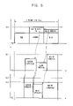
- FIG. 5 is a schematic diagram illustrating a generation of RGBW data according to the present invention with respect to RGB data of an original image signal.
- the upper graph represents an original image signal
- the medium graph represents a 4-color image signal
- a lower graph represents a luminance enhanced image signal according to the present invention.
- X-axis corresponds to one frame
- Y-axis corresponds to a transmittance according to a voltage that is applied to an OCB mode liquid crystal layer.
- a first critical voltage Vc 1 corresponding to liquid crystal molecules of a conventional OCB mode LCD apparatus is substantially greater than a second critical voltage Vc 2 corresponding to liquid crystal molecules of the OCB mode LCD apparatus according to the present embodiment.
- a transmittance of the second critical voltage Vc 2 is greater than that of the first critical voltage Vc 1 .
- RGB data of the original image signals that are adopted for the 3-field driving method are, respectively, to three field intervals divided into same interval during one frame, that is about 16.7 millisecond (ms).
- the one frame corresponding to the conventional 4-field driving method includes four field intervals that are divided into same intervals.
- the RGB data of the same area of the original RGB data are corresponding to the same area of the white data.
- the RGB data corresponding to a difference of the area are displayed during RGB fields corresponding to the 4-field driving.
- the area of the RGB data is defined by a field time interval and a threshold voltage, and substantially corresponds to a transmittance.
- a color data may not correspond to a red field interval of the R data
- G data corresponding to a first difference area “g” corresponds to a green field interval of the G data
- B data corresponding to a second difference area “b” corresponds to a blue field interval of a B data
- the same W data corresponds to a white field interval corresponding to W data.
- the black voltage is applied to the liquid crystal layer such that a black image is displayed.
- a relatively high voltage is applied to the liquid crystal layer to display black image.
- a green field interval following the red field interval a green LED emits, a predetermined voltage corresponding to the first difference area “g” is applied to the liquid crystal layer such that a green image is displayed.
- a blue field interval following the green field interval a blue LED emits, a predetermined voltage corresponding to the second difference area “b” is applied to the liquid crystal layer such that a blue image is displayed.
- a predetermined voltage corresponding to the third difference area “w” is applied to the liquid crystal layer such that a white image is displayed.
- RGB colors that is, 3 colors are displayed just when the LCD apparatus is driven by a 3-field driving method
- 2 colors are displayed just when the LCD apparatus is driven by a 4-field driving method. Therefore, when the LCD apparatus is driven by the 4-field driving method, the color breaking is decreased. Furthermore, the display interval of the white image is greater than the display interval of any given color, so that the luminance of the LCD apparatus is improved.
- the LCD apparatus of the 4-field driving method has a relatively reduced charging time so the time for the liquid crystal layer to respond is reduced.
- the response time of the liquid crystal layer will be described in the following FIG. 6 .
- FIG. 6 is a waveform diagram showing a charging characteristic of a liquid crystal layer in accordance with a 3-field driving method and a 4-field driving method.
- the upper waveform is the charging characteristics of the 3-field driving method and the lower waveform is the charging characteristics of the 4-field driving method.
- the liquid crystal layer that is driven by the 3-field driving method has a response time of a first time x 1 and a first transmittance y 1 .
- the liquid crystal layer that is driven by the 4-field driving method has a shorter response time x 2 to achieve the second transmittance y 2 (that is less than y 1 ).
- the transmittance may be enhanced. This is due to the fact that a field of a black voltage exists in the 4-field driving method. When a field corresponding to the black voltage is applied to the OCB mode LCD apparatus, a critical voltage Vc is decreased such that the transmittance may be enhanced.
- FIGS. 7A to 7E are schematic diagrams showing applying methods of various data that is applied to an OCB mode liquid crystal layer.
- FIG. 8 is a voltage-transmittance (VT) curve of various data that is applied in FIGS. 7A to 7E .
- VT voltage-transmittance
- a normal degradation data NOM corresponding to n-numbered frame data is sent to the LCD panel during one frame, that is about 16.7 ms.
- a white gradation voltage is defined as a minimum voltage (about 2V) that is greater than a critical voltage Vc (about 1.8V) and that remains in a bend alignment state.
- a black gradation voltage is defined as a maximum voltage (about 6V) that remains in a bend alignment state. That is, the white gradation voltage should be greater than the critical voltage Vc in order to drive the LCD apparatus in a static OCB mode.
- the normal gradation voltage NOM is sent to the LCD panel during an earlier 1 ⁇ 2 frame period (about 8.35 ms), and a black gradation voltage BLA is sent to the LCD panel during a later 1 ⁇ 2 frame period (about 8.35 ms).
- the normal gradation voltage NOM corresponds to n-numbered frame data.
- the black gradation voltage BLA is used for enhancing a visibility of a moving image. Referring to the VT curve corresponded to a duty cycle of about 1:1 as shown in FIG. 8 , the bend state is maintained even though the white gradation voltage is 0V.
- the duty cycle is defined as a display ratio between a normal image and a black image displayed in a display area of one frame period.
- the normal gradation voltage NOM is sent to the LCD panel during an earlier 2 ⁇ 3 frame period (about 12.52 ms), and a black gradation voltage BLA is sent to the LCD panel during a later 1 ⁇ 3 frame period (about 4.18 ms).
- the normal gradation voltage NOM corresponds to n-numbered frame data.
- the black gradation voltage BLA is used for enhancing a visibility of a moving image.
- the bend state is maintained even though the white gradation voltage is 0V. Furthermore, luminance characteristics of the duty cycle of about 2:1 are increased than that of the duty cycle of about 1:1.
- the normal gradation voltage NOM is sent to the LCD panel during an earlier 4 ⁇ 5 frame period (about 13.36 ms), and a black gradation voltage BLA is sent to the LCD panel during a later 1 ⁇ 5 frame period (about 3.34 ms).
- the normal gradation voltage NOM corresponds to n-numbered frame data.
- the black gradation voltage BLA is used for enhancing the visibility of the moving image.
- the bend state is maintained even though the white gradation voltage is 0V. Furthermore, luminance characteristics of the duty cycle of about 4:1 are increased than that of the duty cycle of about 1:1.
- the normal gradation voltage NOM is sent to the LCD panel during an earlier 8/9 frame period (about 14.8 ms), and a black gradation voltage BLA is sent to the LCD panel during a later 1/9 frame period (about 1.86 ms).
- the normal gradation voltage NOM corresponds to n-numbered frame data.
- the black gradation voltage BLA is used for enhancing the visibility of the moving image.
- the bend state is maintained even though the white gradation voltage is 0V. Furthermore, luminance characteristics of the duty cycle of about 8:1 are increased than that of the duty cycle of about 1:1.
- a time interval sent the black gradation voltage BLA is about 1.5 ms to about 8 ms.
- the normal gradation voltage is sent to the LCD panel, and then the black gradation voltage is sent to the LCD panel.
- the black gradation voltage may be sent to the LCD panel, and then the normal gradation voltage may be sent to the LCD panel.
- the bend state is maintained even though the white gradation voltage is 0V.
- the black gradation voltage is inserted into the one frame.
- the transmittance of the OCB mode LCD apparatus is enhanced.
- a number of conditions should be satisfied to extend the white field. This is because a transmittance increasing factor and a transmittance decreasing factor coexist in the OCB mode LCD apparatus.
- the critical voltage Vc may be decreased or removed. Therefore, a condition that maintains a bend alignment state is satisfied, so that the transmittance of the OCB mode LCD apparatus is increased.
- the field time interval corresponding to the other colors data, except the white color data is decreased, however a critical voltage Vc corresponding to the other colors data is fixed.
- the size that is defined by the field time interval and the critical voltage is decreased.
- the size corresponds to a transmittance, so that decreasing the size corresponds to decreasing the transmittance.
- the inserting time of the black data is about 8.3 ms, and the critical voltage of the OCB mode liquid crystal molecules is about 0.2V.
- the inserting time of the black data is about 5.6 ms, and the critical voltage of the OCB mode liquid crystal molecules is about 0.2V.
- the inserting time of the black data is about 3.3 ms, and the critical voltage of the OCB mode liquid crystal molecules is about 0.2V.
- the inserting time of the black data is about 1.9 ms, and the critical voltage of the OCB mode liquid crystal molecules is about 0.3V.
- a field time interval of each sub-field is about 4.17 ms.
- a response speed of the liquid crystal is about 0.5 ms to about 1 ms, no more than about 3 ms is substantially an applying time of the black voltage. That is, a duty cycle of the black interval is about 4:1.
- each of the field intervals of the RGB data should be maintained at about 2 ms.
- ‘1.9 ms’ is an allowable time to insert the black data in the duty cycle 8:1
- ‘1 ms’ is a response time of a liquid crystal
- ‘3’ is a number of sub-fields corresponding to each of the RGB data.
- ‘16.7 ms’ is a time of one frame when the LCD apparatus is driven with a normal operation frequency, such as 60 Hz
- ‘8.7 ms’ is a total of minimum requiring time interval of each of the RGB frame
- ‘8 ms’ is a maximum allowable time interval of the white frame.
- the white field may be extended to about 8 ms.
- a conventional OCB mode LCD apparatus is driven by a full-white voltage of about 2.0V for full-white gradation, because the critical voltage Vc exists in the conventional OCB mode LCD apparatus, which is established for maintaining a bend alignment state of the liquid crystal layer.
- the OCB mode LCD apparatus is driven by a full-white voltage of about 0.2V to about 0.6V.
- the luminance of the full-white gradation is about 580 cd/m 2 in the conventional OCB mode LCD apparatus, however that of the full-white gradation is about 840 cd/m 2 in the OCB mode LCD apparatus employing the impulsive driving method. Therefore, a luminance of RGB data according to the present invention is increased to about 44.8% in comparison to a luminance of RGB data according to the conventional OCB mode LCD apparatus.
- FIG. 9 is a schematic diagram showing an input sequence of RGBW data of the LCD apparatus and an emitting sequence of the RGBW emitting elements.
- one frame is divided in to five numbers of field intervals.
- timing controller 110 provides the light emitting section 150 with a red light control signal RC, a green light control signal GC and a blue light control signal BC having a ground level, during a first field interval of the first frame.
- Timing controller 110 provides the light emitting section 150 with the green light control signal GC having a relatively high level, during a second field interval of the first frame.
- Timing controller 110 provides the light emitting section 150 with the blue light control signal BC having a relatively low level, during a third field interval of the first frame.
- Timing controller 110 provides the light emitting section 150 with red, green and blue light control signals RC, GC and BC having a relatively medium level, during the fourth field interval and the fifth field interval of the first frame.
- a total of the first to third field intervals is about 8.7 ms, and a total of the fourth and fifth field intervals is about 8 ms.
- timing controller 110 provides light emitting section 150 with a green light control signal GC having a relatively low level, during a first field interval of a second frame.
- Timing controller 110 provides the light emitting section 150 with a red light control signal RC, a green light control signal GC and a blue light control signal BC having a ground level, during a second field interval of the second frame.
- Timing controller 110 provides the light emitting section 150 with a red light control signal RC, a green light control signal GC and a blue light control signal BC having a relatively medium level, during a third field interval and a fourth field interval of the second frame.
- Timing controller 110 provides the light emitting section 150 with the red control signals RC having a relatively high level, during fifth field interval of the second frame.
- a total of the first, second and fifth field interval is about 8.7 ms
- a total of the third and fourth field interval is about 8 ms.
- timing controller 110 provides the light emitting section 150 with a blue light control signal BC having a relatively medium level, during a first field interval of a third frame.
- Timing controller 110 provides the light emitting section 150 with a red light control signal RC, a green light control signal GC and a blue light control signal BC having a relatively medium level, during a second field interval and a third field interval of the third frame.
- Timing controller 110 provides the light emitting section 150 with the blue light control signal BC having a relatively high level, during a third field interval of the fourth frame.
- Timing controller 110 provides the light emitting section 150 with a red light control signal RC, a green light control signal GC and a In blue light control signal BC having a ground level, during fifth field interval of the third frame.
- a total of the first, fourth and fifth field interval is about 8.7 ms
- a total of the second and third field interval is about 8 ms.
- FIG. 10 is a waveform diagram showing an example of an emitting sequence of the emitting elements in FIG. 1 .
- the upper graph shows a providing time of the RGB data to a LCD panel 140 including 8 ⁇ 8 pixels, during one frame “T”, and the lower graph shows a light emitting sequence of the RGB light emitting elements synchronized to the RGB data.
- the one frame period “T” includes a first field interval, a second field interval, a third field interval and a fourth field interval.
- no data is applied to the LCD panel 140 during a first field interval of a first frame period.
- the light emitting elements that are disposed rear of the LCD panel 140 is not emitted.
- a plurality of green data is provided to the LCD panel 140 during a second field interval of the first frame period.
- a charging ratio corresponded to the green data of the liquid crystal capacitor Clc is about 90%, the green light emitting element emits a green light beam.
- the green light emitting element emits the green light beam.
- the green light emitting element emits the green light beam.
- the green light emitting element emits the green light beam.
- a plurality of blue data is provided to the LCD panel 140 during a third field interval of the first frame period.
- a charging ratio corresponding to the blue data of the liquid crystal capacitor Clc is about 90%, the blue light emitting element emits a blue light beam.
- the blue light emitting element emits the blue light beam.
- the blue light emitting element emits the blue light beam.
- the blue light emitting element emits the blue light beam.
- a plurality of white data is provided to the LCD panel 140 during a fourth field interval of the first frame period.
- a charging ration corresponded to the white data of the liquid crystal capacitor Clc is about 90%
- the red, green and blue light emitting elements 154 R, 154 G and 154 B simultaneously emit the red, green and blue light beams.
- FIG. 11 is a block diagram illustrating a liquid crystal display apparatus according to another exemplary embodiment of the present invention.
- FIG. 12 is a waveform diagram showing an example of an emitting sequence of the emitting element in FIG. 11 .
- an LCD apparatus including a backlight assembly having RGBW light emitting elements is illustrated.
- an LCD apparatus includes a timing controller 210 , a data driving section 120 , a gate driving section 130 , an LCD panel 140 and a light extracting section 250 .
- the timing controller 210 receives an original image signal RGB, various synchronizing signals Hsync and Vsync, a data enable signal DE and a main clock signal MCLK from an external device such as a graphic controller.
- Hsync denotes a horizontal synchronizing signal
- Vsync denotes a vertical synchronizing signal.
- the timing controller 210 provides data driving section 120 with image signals R′′G′′B′′W′′ having an enhanced luminance and data driving signals LOAD and STH for outputting the image signals R′′G′′B′′W′′.
- LOAD controls a loading of the second data signal DATA 2
- STH denotes a horizontal start signal that controls a start of one horizontal line.
- the timing controller 210 includes, for example, a 4-color converting section 112 and a pulse width/level converting section 114 for converting the original image signal RGB into a luminance enhanced image signal R′′G′′B′′W′′.
- the 4-color converting section 112 and pulse width/level converting section 114 of the present embodiment are the same as in FIG. 1 .
- the same reference numerals will be used to refer to the same or like parts as those described in FIG. 1 and any further explanation concerning the above elements will be omitted.
- Timing controller 210 provides the date driving section 130 with gate driving signals GCLK and STV and gate turn-on/off voltages VON and VOFF.
- GCLK denotes a gate clock signal
- STV denotes a vertical start signal representing a start of one frame.
- Timing controller 210 provides light emitting section 250 with a red light control signal RC, a green light control signal GC, a blue light control signal BC and a white light control signal WC in response to the vertical start signal STV.
- the vertical start signal STV is a synchronization signal that induces a start of one frame.
- the one frame includes a first field interval, a second field interval, a third field interval and a fourth field interval.
- a total of the first to third field intervals is about 8.7 ms
- the fourth field is about 8 ms.
- timing controller 210 provides the light emitting section 250 with the red, green, blue and white light control signals RC, GC, BC and WC having a ground level, during the first field interval of the first frame.
- Timing controller 210 provides the light emitting section 250 with the green light control signal GC having a high level, during the second field interval of the first frame.
- the timing controller 210 provides the light emitting section 250 with the blue light control signal BC having a high level, during the third field interval of the first frame.
- Timing controller 210 provides the light emitting section 250 with the white light control signal WC having a high level, during the fourth field interval of the first frame.
- timing controller 210 provides the light emitting section 250 with the green light control signal GC having a high level, during the first field interval of the second frame.
- Timing controller 210 provides the light emitting section 250 with the red, green, blue and white light control signals RC, GC, BC and WC having a ground level, during the second field interval of the second frame.
- Timing controller 210 provides the light emitting section 250 with the white light control signal WC having a high level, during the third field interval of the second frame.
- Timing controller 210 provides the light emitting section 250 with the blue light control signal BC having a high level, during the fourth field interval of the second frame.
- timing controller 210 provides the light emitting section 250 with the blue light control signal BC having a high level, during the first field interval of the third frame.
- Timing controller 210 provides light emitting section 250 with the white light control signal WC having a high level, during the second field interval of the third frame.
- Timing controller 210 provides light emitting section 250 with the red light control signal RC having a high level, during the third field interval of the third frame.
- Timing controller 210 provides light emitting section 250 with the red, green, blue and white light control signals RC, GC, BC and WC having a ground level, during the fourth field interval of the third frame.
- Light emitting section 250 includes a power supplying section 252 and a light emitting part 254 .
- Light emitting section 250 non-sequentially emits a red light beam, a green light beam, a blue light beam and a white light beam in response to the red, green, blue and white light control signals RC, GC, BC and WC provided by the timing controller 210 .
- light emitting section 250 may emit a predetermined light beam during a third field interval of the previous frame, and may emit the predetermined light beam during a second field interval of the present frame. Continuously, light emitting section 250 may emit the predetermined light beam during the first field interval of the next frame.
- Power supplying section 252 provides light emitting part 254 with a first current Rl for emitting a red light beam, a second current Gl for emitting a green light beam, a third current Bl for emitting a blue light beam and a fourth current Wl for emitting a white light beam in response to the red, green, blue and white light control signals RC, GC, BC and WC provided by timing controller 210 .
- Light emitting part 254 includes a red light emitting element 254 R, a green light emitting element 254 G, a blue light emitting element 254 B and a white light emitting element 254 W.
- Light emitting element includes a light emitting diode (LED).
- the red light emitting element 254 R provides the LCD panel 140 with a red light beam in response to the first current Rl.
- the green light emitting element 254 G provides the LCD panel 140 with a green light beam in response to the second current Gl.
- the blue light emitting element 254 B provides the LCD panel 140 with a blue light beam in response to the third current Bl.
- the white light emitting element 254 W provides the LCD panel 140 with a white light beam in response to the fourth current Wl.
- the color filter-less LCD apparatus having a 4-field driving method that emits RGBW data employs an OCB mode liquid crystal, so that the field time interval corresponding to white data is assured. Therefore, response speed, charging ratio and transmittance of the OCB mode liquid crystal molecules are improved.
Abstract
Description
Rγ=aR γ
Gγ=aR γ
Rγ=aB γ Expression 1
Rγ′=SRγ
Gγ′=SGγ
Bγ′=
Wγ′=aGmaxγ,ifMin(R′γ,Gγ,Bγ)≧aGmaxγ
Wγ′=Min(R′γ, Gγ,Bγ),
Rγ*=Rγ′−Wγ′
Gγ*=Gγ′−Wγ′
Bγ*=Bγ′−Wγ′
Wγ*=Wγ′
Wγ=Min(Rγ, Gγ, Bγ) Expression 6
Rγ′=Rγ−Wγ
Gγ′=Gγ′Wγ
Bγ′=Bγ−Wγ
Wγ′=
| TABLE 1 | ||
| Ratio of a black | Inserting time of | Critical |
| interval (DUTY CYCLE) | a black data | voltage (Vc) |
| 50% (1:1) | 8.3 ms | 0.2 V |
| 33% (2:1) | 5.6 ms | 0.2 V |
| 20% (4:1) | 3.3 ms | 0.2 |
| 11% (8:1) | 1.9 ms | 0.3 V |
(1.9 ms+1 ms)×3=8.7 ms
16.7 ms−8.7 ms=8 ms
Claims (20)
Applications Claiming Priority (3)
| Application Number | Priority Date | Filing Date | Title |
|---|---|---|---|
| KR1020060018061A KR101219143B1 (en) | 2006-02-24 | 2006-02-24 | Liquid crystal display apparatus and method of driving thereof |
| KR2006-18061 | 2006-02-24 | ||
| KR10-2006-0018061 | 2006-02-24 |
Publications (2)
| Publication Number | Publication Date |
|---|---|
| US20070200807A1 US20070200807A1 (en) | 2007-08-30 |
| US8089441B2 true US8089441B2 (en) | 2012-01-03 |
Family
ID=38443509
Family Applications (1)
| Application Number | Title | Priority Date | Filing Date |
|---|---|---|---|
| US11/710,185 Active 2029-08-17 US8089441B2 (en) | 2006-02-24 | 2007-02-23 | Liquid crystal display apparatus and driving method therefor |
Country Status (2)
| Country | Link |
|---|---|
| US (1) | US8089441B2 (en) |
| KR (1) | KR101219143B1 (en) |
Families Citing this family (19)
| Publication number | Priority date | Publication date | Assignee | Title |
|---|---|---|---|---|
| US7750887B2 (en) * | 2006-12-21 | 2010-07-06 | Itt Manufacturing Enterprises, Inc. | Displays with large dynamic range |
| KR101604482B1 (en) * | 2008-08-14 | 2016-03-25 | 엘지디스플레이 주식회사 | Liquid Crystal Display and Driving Method Thereof |
| KR101399304B1 (en) * | 2009-10-08 | 2014-05-28 | 엘지디스플레이 주식회사 | Liquid crystal display device and method of driving the same |
| US9077915B2 (en) * | 2010-04-07 | 2015-07-07 | Projectiondesign As | Interweaving of IR and visible images |
| KR20120133432A (en) * | 2011-05-31 | 2012-12-11 | 삼성디스플레이 주식회사 | Organic Light Emitting Display Device and Driving Method Thereof |
| KR101859481B1 (en) * | 2011-12-26 | 2018-06-29 | 엘지디스플레이 주식회사 | Display device and method for driving the same |
| KR101914936B1 (en) * | 2011-12-29 | 2018-11-06 | 삼성디스플레이 주식회사 | Method and circuit for compensating gamma reference voltages |
| US9093036B2 (en) * | 2012-05-14 | 2015-07-28 | Samsung Display Co., Ltd. | Determining size of sub pixels in a multi primary display for maximizing white point luminance level |
| KR101489639B1 (en) * | 2012-09-25 | 2015-02-06 | 엘지디스플레이 주식회사 | Timing controller, its driving method, flat panel display device |
| KR101489637B1 (en) | 2012-09-25 | 2015-02-04 | 엘지디스플레이 주식회사 | Timing controller, its driving method, and flat panel display device |
| JP2014074752A (en) * | 2012-10-03 | 2014-04-24 | Sony Corp | Image display device and method of driving image display device, signal generation device, signal generation program and signal generation method |
| US9230345B2 (en) * | 2013-10-02 | 2016-01-05 | Pixtronix, Inc. | Display apparatus configured for display of lower resolution composite color subfields |
| KR102106271B1 (en) * | 2013-10-24 | 2020-05-06 | 삼성디스플레이 주식회사 | Display apparatus and driving method thereof |
| WO2015072213A1 (en) * | 2013-11-13 | 2015-05-21 | シャープ株式会社 | Field sequential liquid crystal display device and method for driving same |
| KR102150290B1 (en) * | 2014-01-10 | 2020-09-02 | 삼성디스플레이 주식회사 | Liquid display device |
| TWI559730B (en) * | 2014-08-25 | 2016-11-21 | 群創光電股份有限公司 | 3d flame display system and its method |
| WO2018062091A1 (en) * | 2016-09-30 | 2018-04-05 | シャープ株式会社 | Field sequential image display device and image display method |
| US20200027418A1 (en) * | 2018-07-17 | 2020-01-23 | Samsung Display Co., Ltd. | Display device and driving method of the same |
| JP2022136571A (en) * | 2021-03-08 | 2022-09-21 | セイコーエプソン株式会社 | display system |
Citations (9)
| Publication number | Priority date | Publication date | Assignee | Title |
|---|---|---|---|---|
| US6317112B1 (en) * | 1994-12-22 | 2001-11-13 | Displaytech, Inc. | Active matrix liquid crystal image generator with hybrid writing scheme |
| US20020057253A1 (en) * | 2000-11-09 | 2002-05-16 | Lim Moo-Jong | Method of color image display for a field sequential liquid crystal display device |
| US6392620B1 (en) * | 1998-11-06 | 2002-05-21 | Canon Kabushiki Kaisha | Display apparatus having a full-color display |
| US6570554B1 (en) * | 1999-11-08 | 2003-05-27 | Fujitsu Limited | Liquid crystal display |
| US6803894B1 (en) * | 2000-03-08 | 2004-10-12 | Hitachi, Ltd. | Liquid crystal display apparatus and method using color field sequential driving method |
| US20040246275A1 (en) * | 2003-01-29 | 2004-12-09 | Fujitsu Limited | Display device and display method |
| US20060017713A1 (en) * | 2004-07-23 | 2006-01-26 | Lg Philips Lcd Co., Ltd. | Driving circuit of liquid crystal display device and method for driving the same |
| US20070222743A1 (en) * | 2006-03-22 | 2007-09-27 | Fujifilm Corporation | Liquid crystal display |
| US20100103205A1 (en) * | 2008-10-28 | 2010-04-29 | Seiko Epson Corporation | Driving method and electro-optical apparatus |
-
2006
- 2006-02-24 KR KR1020060018061A patent/KR101219143B1/en active IP Right Grant
-
2007
- 2007-02-23 US US11/710,185 patent/US8089441B2/en active Active
Patent Citations (9)
| Publication number | Priority date | Publication date | Assignee | Title |
|---|---|---|---|---|
| US6317112B1 (en) * | 1994-12-22 | 2001-11-13 | Displaytech, Inc. | Active matrix liquid crystal image generator with hybrid writing scheme |
| US6392620B1 (en) * | 1998-11-06 | 2002-05-21 | Canon Kabushiki Kaisha | Display apparatus having a full-color display |
| US6570554B1 (en) * | 1999-11-08 | 2003-05-27 | Fujitsu Limited | Liquid crystal display |
| US6803894B1 (en) * | 2000-03-08 | 2004-10-12 | Hitachi, Ltd. | Liquid crystal display apparatus and method using color field sequential driving method |
| US20020057253A1 (en) * | 2000-11-09 | 2002-05-16 | Lim Moo-Jong | Method of color image display for a field sequential liquid crystal display device |
| US20040246275A1 (en) * | 2003-01-29 | 2004-12-09 | Fujitsu Limited | Display device and display method |
| US20060017713A1 (en) * | 2004-07-23 | 2006-01-26 | Lg Philips Lcd Co., Ltd. | Driving circuit of liquid crystal display device and method for driving the same |
| US20070222743A1 (en) * | 2006-03-22 | 2007-09-27 | Fujifilm Corporation | Liquid crystal display |
| US20100103205A1 (en) * | 2008-10-28 | 2010-04-29 | Seiko Epson Corporation | Driving method and electro-optical apparatus |
Also Published As
| Publication number | Publication date |
|---|---|
| KR20070088000A (en) | 2007-08-29 |
| US20070200807A1 (en) | 2007-08-30 |
| KR101219143B1 (en) | 2013-01-07 |
Similar Documents
| Publication | Publication Date | Title |
|---|---|---|
| US8089441B2 (en) | Liquid crystal display apparatus and driving method therefor | |
| JP4436790B2 (en) | Liquid crystal display device having OCB mode and driving method thereof | |
| US7030848B2 (en) | Liquid crystal display | |
| US7499016B2 (en) | Liquid crystal display device | |
| US8174485B2 (en) | Liquid crystal display device and driving method thereof | |
| US7453430B2 (en) | Field sequential liquid crystal display and a driving method thereof | |
| US20070146299A1 (en) | Liquid crystal display and method for driving the same | |
| KR20200059700A (en) | Display Apparatus and Driving Method of the same | |
| US7429971B2 (en) | Liquid crystal display and a driving method thereof | |
| US7602360B2 (en) | Liquid crystal display and a driving method thereof | |
| US20110102476A1 (en) | Driver of field sequential display and driving method thereof | |
| US7352351B2 (en) | Active matrix-type display device and method of driving the same | |
| JP2010039136A (en) | Liquid crystal display | |
| US20110310136A1 (en) | Liquid crystal display and driving method thereof | |
| JP2003316335A (en) | Liquid crystal display device and method for driving the same | |
| KR20040042402A (en) | Liquid Crystal Display And Driving Method Thereof | |
| KR100848103B1 (en) | Liquid crystal display for performing time division color display and backlight unit therefor | |
| KR101282288B1 (en) | Two color sequential plus driving method | |
| KR100627385B1 (en) | Liquid crystal display | |
| JP3793215B2 (en) | Color LCD device | |
| KR101035916B1 (en) | Circuit for driving of Liquid Crystal Display Device | |
| US20080284717A1 (en) | Electro-optical device, method for driving the same, and electronic machine | |
| KR20060012989A (en) | Liquid crystal display | |
| KR20100124970A (en) | Liquid crystal display device and driving method thereof | |
| KR20170005942A (en) | Liquid crystal display device and driving method thereof |
Legal Events
| Date | Code | Title | Description |
|---|---|---|---|
| AS | Assignment |
Owner name: SAMSUNG ELECTRONICS CO., LTD., KOREA, REPUBLIC OF Free format text: ASSIGNMENT OF ASSIGNORS INTEREST;ASSIGNORS:LEE, CHANG-HUN;HAN, EUN-HEE;LEE, JUN-WOO;REEL/FRAME:019038/0602 Effective date: 20061228 |
|
| FEPP | Fee payment procedure |
Free format text: PAYOR NUMBER ASSIGNED (ORIGINAL EVENT CODE: ASPN); ENTITY STATUS OF PATENT OWNER: LARGE ENTITY |
|
| STCF | Information on status: patent grant |
Free format text: PATENTED CASE |
|
| AS | Assignment |
Owner name: SAMSUNG DISPLAY CO., LTD, KOREA, REPUBLIC OF Free format text: ASSIGNMENT OF ASSIGNORS INTEREST;ASSIGNOR:SAMSUNG ELECTRONICS, CO., LTD;REEL/FRAME:028989/0523 Effective date: 20120904 |
|
| FPAY | Fee payment |
Year of fee payment: 4 |
|
| MAFP | Maintenance fee payment |
Free format text: PAYMENT OF MAINTENANCE FEE, 8TH YEAR, LARGE ENTITY (ORIGINAL EVENT CODE: M1552); ENTITY STATUS OF PATENT OWNER: LARGE ENTITY Year of fee payment: 8 |
|
| MAFP | Maintenance fee payment |
Free format text: PAYMENT OF MAINTENANCE FEE, 12TH YEAR, LARGE ENTITY (ORIGINAL EVENT CODE: M1553); ENTITY STATUS OF PATENT OWNER: LARGE ENTITY Year of fee payment: 12 |