US8089434B2 - Electroded polymer substrate with embedded wires for an electronic display - Google Patents
Electroded polymer substrate with embedded wires for an electronic display Download PDFInfo
- Publication number
- US8089434B2 US8089434B2 US11/609,131 US60913106A US8089434B2 US 8089434 B2 US8089434 B2 US 8089434B2 US 60913106 A US60913106 A US 60913106A US 8089434 B2 US8089434 B2 US 8089434B2
- Authority
- US
- United States
- Prior art keywords
- sheet
- wire
- electroded
- polymer
- display
- Prior art date
- Legal status (The legal status is an assumption and is not a legal conclusion. Google has not performed a legal analysis and makes no representation as to the accuracy of the status listed.)
- Expired - Fee Related, expires
Links
Images


Classifications
-
- G—PHYSICS
- G02—OPTICS
- G02F—OPTICAL DEVICES OR ARRANGEMENTS FOR THE CONTROL OF LIGHT BY MODIFICATION OF THE OPTICAL PROPERTIES OF THE MEDIA OF THE ELEMENTS INVOLVED THEREIN; NON-LINEAR OPTICS; FREQUENCY-CHANGING OF LIGHT; OPTICAL LOGIC ELEMENTS; OPTICAL ANALOGUE/DIGITAL CONVERTERS
- G02F1/00—Devices or arrangements for the control of the intensity, colour, phase, polarisation or direction of light arriving from an independent light source, e.g. switching, gating or modulating; Non-linear optics
- G02F1/01—Devices or arrangements for the control of the intensity, colour, phase, polarisation or direction of light arriving from an independent light source, e.g. switching, gating or modulating; Non-linear optics for the control of the intensity, phase, polarisation or colour
- G02F1/13—Devices or arrangements for the control of the intensity, colour, phase, polarisation or direction of light arriving from an independent light source, e.g. switching, gating or modulating; Non-linear optics for the control of the intensity, phase, polarisation or colour based on liquid crystals, e.g. single liquid crystal display cells
- G02F1/133—Constructional arrangements; Operation of liquid crystal cells; Circuit arrangements
- G02F1/1333—Constructional arrangements; Manufacturing methods
- G02F1/1343—Electrodes
- G02F1/13439—Electrodes characterised by their electrical, optical, physical properties; materials therefor; method of making
-
- B—PERFORMING OPERATIONS; TRANSPORTING
- B82—NANOTECHNOLOGY
- B82Y—SPECIFIC USES OR APPLICATIONS OF NANOSTRUCTURES; MEASUREMENT OR ANALYSIS OF NANOSTRUCTURES; MANUFACTURE OR TREATMENT OF NANOSTRUCTURES
- B82Y20/00—Nanooptics, e.g. quantum optics or photonic crystals
-
- G—PHYSICS
- G02—OPTICS
- G02F—OPTICAL DEVICES OR ARRANGEMENTS FOR THE CONTROL OF LIGHT BY MODIFICATION OF THE OPTICAL PROPERTIES OF THE MEDIA OF THE ELEMENTS INVOLVED THEREIN; NON-LINEAR OPTICS; FREQUENCY-CHANGING OF LIGHT; OPTICAL LOGIC ELEMENTS; OPTICAL ANALOGUE/DIGITAL CONVERTERS
- G02F1/00—Devices or arrangements for the control of the intensity, colour, phase, polarisation or direction of light arriving from an independent light source, e.g. switching, gating or modulating; Non-linear optics
- G02F1/01—Devices or arrangements for the control of the intensity, colour, phase, polarisation or direction of light arriving from an independent light source, e.g. switching, gating or modulating; Non-linear optics for the control of the intensity, phase, polarisation or colour
- G02F1/13—Devices or arrangements for the control of the intensity, colour, phase, polarisation or direction of light arriving from an independent light source, e.g. switching, gating or modulating; Non-linear optics for the control of the intensity, phase, polarisation or colour based on liquid crystals, e.g. single liquid crystal display cells
- G02F1/133—Constructional arrangements; Operation of liquid crystal cells; Circuit arrangements
- G02F1/1333—Constructional arrangements; Manufacturing methods
- G02F1/133305—Flexible substrates, e.g. plastics, organic film
-
- G—PHYSICS
- G02—OPTICS
- G02F—OPTICAL DEVICES OR ARRANGEMENTS FOR THE CONTROL OF LIGHT BY MODIFICATION OF THE OPTICAL PROPERTIES OF THE MEDIA OF THE ELEMENTS INVOLVED THEREIN; NON-LINEAR OPTICS; FREQUENCY-CHANGING OF LIGHT; OPTICAL LOGIC ELEMENTS; OPTICAL ANALOGUE/DIGITAL CONVERTERS
- G02F2202/00—Materials and properties
- G02F2202/36—Micro- or nanomaterials
Definitions
- the invention pertains to the field of electronic displays, in particular creating an electroded plane in the flat panel display.
- An electro-optic material is defined as a material that changes state in an electric field. Some of these materials can be passively addressed or simply addressed by sandwiching the electro-optic material between two orthogonal arrays of electrodes. However, this passive addressing scheme requires that the electro-optic material has a threshold or its optical properties have an abrupt change over a small change in applied voltage. Most liquid crystal (LC) materials have a steep enough threshold that allows them to be passively addressed.
- LC liquid crystal
- the electro-optic material does not have a voltage threshold or its threshold is not steep enough (the voltage to totally modulate the material has to be less than twice the voltage of where the materials electro-optic properties start to change), then the electro-optic material has to be actively addressed.
- Active addressing means that a switch, like a transistor, that has a voltage threshold is used to place the voltage across the electro-optic material.
- Other active addressing switches that have been used are diodes, plasmas, and micro-electro-mechanical systems (MEMS). Active addressing is also used in cases that require video rate images because passive addressing requires that a line at a time addressing scheme is used and therefore the speed to update the image is limited to the number of lines in the display times the minimum response time of the electro-optic media.
- electro-optic materials There are several different types of electro-optic materials.
- the most well known and widely used electro-optic materials are liquid crystal molecules.
- liquid crystal molecules In the liquid crystal family, a vast range of molecules could potentially be used to create the electro-optic modulated material.
- Some of these liquid crystal molecules include, but are not limited to, twisted nematic, cholesteric-nematic, dichroic dye (or guest-host), dynamic scattering mode, smectic, and polymer dispersed. Most of these liquid crystal molecules require other films, such as alignment layers, polarizers, and reflective films.
- Electrophoretic material is a suspension of small charged particles in a liquid solution. If the particles have a similar density as the liquid solution, they are not affected by gravity. Therefore the only way to move the particles is using an electric field. By applying a voltage potential across the electrophoretic solution, the charged particles are forced to move in the suspension to one of the contacts. The opposite charge moves the particles in the other direction.
- the electrophoretic suspension is designed such that the particles are a different color than the liquid solution or there are two different colored particles with opposite charge states.
- twisting ball material Another type of electro-optic material is a twisting ball or Gyricon material. It was initially called twisting ball material because it is composed of small bichromal spheres, one side coated black, the other white with opposite charges on the two halves. Therefore, when the twisting ball material is placed in an electric field, the bichromal spheres all rotate to display one optical property of the material and when the opposite voltage is applied, the material displays the other colored state.
- This Gyricon material can also be made in a cylindrical form.
- SPD suspended particle device
- One potential solution for producing large size displays is to use fibers/tubes to create the plasma cells. Using tubes to create a plasma-addressable plasma cell was first disclosed in U.S. Pat. No. 3,964,050, herein incorporated by reference.
- One potential issue in producing large plasma-addressed tubular displays is creating the top column electrode plate.
- This plate has to be composed of an array of lines to address that set the charge in the plasma tubes.
- these electrode lines When addressing a thin electro-optic material like a LC or electrophoretic material, these electrode lines have to be wide enough to spread the charge across the width of the entire pixel.
- the lines also have to be conductive enough to set the charge in the plasma tube so the display can be addressed at video rates.
- a traditional patterned indium tin oxide (ITO) transparent conductor works fine for smaller panels where processing the panel is easy and the lines are short, however to address very large panels, the ITO lines are not conductive enough and patterning of the lines becomes very expensive.
- top electrode plate of a plasma display Connecting a higher conductive metal film electrode to a transparent conductive film to spread the voltage of the electrode is also traditionally used in the top electrode plate of a plasma display (PDP).
- the top PDP plates use a 50 ⁇ m wide by about 1 ⁇ m thick Cr/Cu/Cr stack to carry current and a thin ITO coating to spread the effect of the voltage, hence spreading the firing of the plasma.
- These electrode coatings are evaporated or sputtered and then photolithograph is used to pattern them and they are then etched into lines using a wet etch or a reactive ion etch (RIE).
- RIE reactive ion etch
- Photovoltaic cells also use conductive metal lines connected to transparent conductive coatings to collect the current from the photovoltaic device.
- the use of wire connected to a transparent conductive coating has been disclosed by Nanosolar in U.S. Pat. Nos. 6,936,761 and 7,022,910, herein incorporated by reference, for solar cell applications.
- the invention is a sheet in an electronic display composed of a substrate containing an array of wire electrodes.
- the wire electrodes are preferably electrically connected to patterned transparent conductive electrode lines, as well as methods of making the sheet.
- the wire electrodes which are defined as a highly conductive thread-like or fiber-like material, are used to carry the bulk of the current.
- the wires are preferably formed using a standard wire forming process; they are free standing entities and are not evaporated or deposited on the substrate.
- the wire electrodes are capable of being extended away from the substrate and connected directly to a printed circuit board.
- the transparent conductive electrode (TCE) is used to spread the charge or voltage from the wire electrode across the pixel.
- the TCE is a patterned film and, in most display applications, must be at least 50% transparent, and is preferably ⁇ 90% transparent.
- the TCE is preferably composed of a transparent conductive polymer, nanotubes, or a PVD material like ITO.
- the TCE must form a good electrical connection with the wire electrode (low interface resistance) and must be electrically connected to the wire electrode along most of the length of the electrode.
- the TCE material does not have to have a high conductivity because it only needs to be conductive enough to spread the charge or voltage across the pixel width.
- the substrate that houses the wires/TCE strips is preferably polymer or glass. Use of a thin polymer substrate yields a light, flexible, rugged sheet that can be curved, bent or rolled.
- the electroded surface is preferably flattened.
- the electroded sheet may be used as an addressing plane in a passive or actively addressed display. Alternatively, it may be used as a sustainer layer or column addressing layer in a tubular plasma display.
- the electroded sheet may be used to capacitively address an electro-optic material or capacitively set-up the charge in a panel.
- the electroded layer may also be used as current carrying strips to address materials such as electrochromic materials or organic light emitting materials.
- FIG. 1 schematically shows an array of wire electrodes electrically connected to transparent conductive lines on a substrate.
- FIG. 2 a schematically shows a cross-section of a substrate with an array of transparent conductive lines on a substrate.
- FIG. 2 b schematically shows a cross-section of the structure in FIG. 2 a with wire electrodes added to the transparent conductive lines.
- FIG. 2 c schematically shows a cross-section of the structure in FIG. 2 b with a lockdown film across the wire electrodes.
- FIG. 3 schematically shows a cross-section of wire electrodes imbedded in the surface of a substrate and electrically connected to transparent conductive electrodes (TCEs).
- TCEs transparent conductive electrodes
- FIG. 4 schematically shows a cross-section of wire electrodes imbedded in the surface of a polymer film on a substrate and the wire electrodes electrically connected to TCEs.
- FIG. 5 schematically shows a cross-section of a structure similar to that in FIG. 4 where the wire electrodes are coated with an electronically conductive film.
- FIG. 6 a schematically shows a method of using glass plates to force wires into the surface of a polymer coated substrate.
- FIG. 6 b schematically shows the wires imbedded in the polymer film using the process shown in FIG. 6 a.
- FIG. 6 c schematically shows a process of patterning TCEs on the surface of a substrate.
- FIG. 6 d schematically shows the final electroded sheet with the wire imbedded in a polymer and electrically connected to TCEs.
- FIG. 7 a illustrates a method of placing wire electrodes over TCEs and forcing them to flow into the surface of a polymer.
- FIG. 7 b schematically shows the wires with TCEs with polymer film after the process of FIG. 7 a.
- FIG. 8 a illustrates a method of placing TCE lines over wire electrodes and forcing them to flow into the surface of a polymer.
- FIG. 8 b schematically shows the wires with TCEs with polymer film after the process of FIG. 8 a.
- FIG. 9 is a photograph of a drum showing the process of imbedding wires into a polymer coated PET sheet.
- FIG. 10 schematically illustrates the process of bending a sheet to force wires to flow into a polymer coated substrate.
- FIG 11 a is a photograph of an electroded sheet with the wire electrodes coming out orthogonal to the imbedded wires in the main body of the panel.
- FIG 11 b is a close-up image of FIG. 11 a.
- FIG. 12 a schematically shows an end of an electroded panel with slices and fold lines.
- FIG. 12 b schematically shows the electroded panel in FIG. 12 a with the end folded such that the wire electrodes are coming out orthogonal to the wires in the main body of the panel.
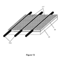
- FIG. 13 schematically represents an electroded sheet formed using a maskless process.
- FIG. 14 a is a schematic of a PET/Polymer sheet with wires positioned on the polymer prior to embedding into the polymer.
- FIG. 14 b is a schematic of the process used to coat the electroded sheet with a transparent conductive electrode.
- FIG. 14 c represents the substrate containing wire electrodes coated with a TCE film using a maskless process.
- FIG. 14 d shows a schematic of the wires embedded into the surface of the polymer substrate.
- FIG. 14 e shows a schematic of the electroded sheet after flattening the surface.
- FIG. 14 f shows a schematic of the electroded sheet after flattening the surface at a higher temperature.
- FIG. 14 g shows the electroded sheet with a film applied to the surface.
- FIG. 15 schematically shows a section of the electroded sheet formed using a web process.
- FIG. 16 a schematically shows a polymer substrate with wires and masks positioned on the surface.
- FIG. 16 b schematically shows the spray process used to coat the transparent conductive electrode material on the wire masked polymer substrate.
- FIG. 16 c schematically shows the electroded sheet after the coating process step.
- FIG. 16 d shows a schematic of the wires and mask embedded into the polymer.
- FIG. 16 e shows a schematic of the wires embedded in the electroded sheet with the mask removed.
- FIG. 16 f shows a schematic of the electroded sheet after flattening the electroded surface.
- FIG. 16 g shows the flattened electroded sheet with a planarizing layer applied to the surface.
- FIG. 16 h shows a planarization layer applied to the surface of the electroded sheet to remove the voids formed between the pairs of wire electrodes.
- FIG. 17 shows islands of transparent conductive polymer interconnected with carbon nanotubes.
- FIG. 18 schematically shows a planar view of an electroded sheet with the wires in a zigzag pattern.
- FIG. 19 schematically shows a planar view of an electroded sheet with the wires in a zigzag pattern formed by tying the wires into a mesh.
- FIG. 20 schematically shows a planar view of an electroded sheet with the wires in a zigzag pattern formed using pins.
- FIG. 21 schematically shows an electroded sheet with a lenticular lens embossed in the surface.
- FIG. 22 schematically shows an electroded sheet with alternating convex and concave lenses embossed into the surface.
- a layer in an electronic display is composed of a substrate 30 containing an array of wire electrodes 31 w electrically connected to patterned transparent conductive electrode 31 f lines, as shown in FIG. 1 .
- the wire electrodes 31 w which are defined as a highly conductive thread-like or fiber-like material, are used to carry the bulk of the current.
- the wires are formed using a standard wire forming process; they are free standing entities and are not evaporated or deposited on the substrate.
- the wire electrodes 31 w are capable of being extended away from the substrate 30 and connected directly to a printed circuit board.
- the transparent conductive electrode (TCE) 31 f is used to spread the charge or voltage from the wire electrode 31 w across a pixel.
- the TCE 31 f is a patterned film that, in most display applications, must be at least 50% transparent, and is preferably over 90% transparent.
- the TCE 31 f must form a good electrical connection with the wire electrode 31 w (low interface resistance) and must be electrically connected to the wire electrode 31 w along most of the length of the electrode.
- the TCE material does not have to have a high conductivity because it only needs to be conductive enough to spread the charge or voltage across the pixel width.
- the substrate 30 that houses the wires/TCEs strips is preferably polymer or glass. Use of a thin polymer substrate 30 yields a light, flexible, rugged sheet that may be curved, bent or rolled.
- the metal has to be deposited using a physical vapor deposition (PVD) process like e-beam evaporation or sputtering, then patterned and etched, which is very costly.
- PVD physical vapor deposition
- Reasonable conductivity may be alternatively achieved using a screen printed silver paste; however, the silver paste has to be fired at elevated temperatures ( ⁇ 400° C.) to achieve any real conductivity, which is much too high a temperature for most polymers.
- Most metal conductive coatings that may be economically applied to polymer substrates have only slightly better conductivity ( ⁇ 5 ⁇ / ⁇ ) compared to the most conductive ITO films ( ⁇ 10 ⁇ / ⁇ ).
- Controlling the addressing of a large display requires that the voltages applied to the electrodes be uniformly brought up to voltage along the entire length of the line especially if grayscale addressing is required.
- the lines have resistance along their length and are capacitively coupled to the orthogonal electrodes.
- the total line capacitance is 62 nF.
- the line was formed using a highly conductive transparent material with a sheet resistance of 100 ⁇ / ⁇ then the resistance of the entire line would be 144 k ⁇ and the line would take 8.9 ms to come up to 98% of the total voltage. If a 0.002′′ diameter copper wire is used to carry the current along the length of the electrode, the line resistance would be reduced to 15 ⁇ and take less than 1 ⁇ s to come up to voltage.
- the wire electrode may be composed of any composition; however using a lower resistivity base material yields the most conductive wire.
- a highly reflective colored material like copper is that it changes the color of the electroded layer.
- One method of removing this reflective copper color is to coat the wire electrode with a black absorbing film. This black absorbing layer has to be electrically conductive so it can make good electrical connection to the transparent conductive electrode (TCE).
- the TCE is preferably composed of one or more of many different materials including, but not limited to, 1) a conductive polymer, such as that sold by Bayer called Baytron®, which also goes by the names of Poly(3,4-ethylenedioxythiophene) poly(styrenesulfonate) or [—CH 2 CH(C 6 H 4 SO 3 H)—] m [—CH 2 CH(C 6 H 4 SO 3 )— 0.33n /[C 6 H 4 O 2 S—] 0.33+ n or PEDT/PSS or PEDOT/PSS; or 2) a nanotube or nanorod coating, such as composed of a single wall carbon nanotube or multiwall carbon nanotubes; or 3) a physical vapor deposited (PVD) film, such as indium tin oxide (ITO) or zinc oxide doped with fluorine (ZnO:F).
- a conductive polymer such as that sold by Bayer called Baytron®, which also goes by the names of Poly(3,4-ethylenedioxythi
- the TCE coatings may be sprayed using a traditional spraying system, however for some of the TCE coatings, like the nanotube solutions, it would be advantageous to use an ultrasonic sprayer to help break the nanotubes apart as they are sprayed.
- the TCE coating may also be sprayed using an airbrush, which is useful in that its spray opening may be very well controlled to only let small particles through, hence controlling any agglomerates.
- the TCE coatings may be printed, which would allow for a low cost method of patterning the lines.
- Some examples of the printing process include, but are not limited to, transfer printing, screen printing, inkjet printing, and intaglio printing.
- the TCE coating may alternatively be brush coated, dip coated, spin coated, extruded, etc. If the TCE coating is a hard coating, like ITO, then a physical vapor deposition (PVD) process is required like e-beam evaporation, sputtering, CVD, arc spraying, etc.
- PVD physical vapor deposition
- the TCE coating has to be patterned into lines to electrically isolate one wire with TCE from its adjacent electrode. If a precision printing process is used, then the TCE coating may be easily patterned during the deposition process. If a directional coating process is used to deposit the TCE film like spraying or some of the PVD processes, then a shadow mask may be used to pattern the TCE film into lines.
- the TCE coating may alternatively be patterned by applying an additional patterned coating, like photoresist, to protect the TCE during an etching process.
- the patterning and etching process may use several different masking films and methods of applying the masking films and may use a wet or dry etching process to pattern the TCE into lines.
- the TCE coating may alternatively be patterned into lines using a lift-off process, where prepattern lines are placed on the substrate at the points where the TCE is to be separated then after the TCE film is deposited, the prepatterned lines are removed separating the TCE film into lines.
- the prepatterned lines may be a polymer, like photoresist, or hard lines like wire, fiber or thread that is removed once coated, which is very similar to a shadow mask.
- the TCE film may alternatively be cut into lines using a scraping tool or cut with a laser. The TCE film could also be cut by forcing wedge shaped line objects down into the coating.
- Adjacent TCE coatings may alternatively be electrically isolated by coating the film along the separation lines with a material the reacts with the TCE to destroy the conductive nature of the film.
- the conductive nature of the TCE film may also be destroyed using heat from a laser beam.
- FIG. 2 shows a method of forming the electroded sheet where the wires 31 w and the TCEs 31 f are placed on a thin polymer or glass substrate 30 and locked down onto the substrate with a film or coating 38 .
- This electrode configuration allows for electrical communication with the rest of the display through the thin polymer or glass substrate 30 .
- This structure requires a voltage drop across the thin substrate, but if the thickness of the substrate is very uniform, then the electric field is very uniform across the pixel and panel.
- FIG. 2 a shows the first step in the process where the TCEs 31 f are deposited in a pattern on the substrate 30 .
- FIG. 2 b shows wire electrodes 31 w applied to the TCEs 31 f .
- a lock down coating 38 is applied over the electrodes to hold them in place, as shown in FIG. 2 c .
- the patterned TCEs 31 f do not have to be wide lines, but may have structure associated with them, such as sometimes used in a sustainer plate for a plasma display like a tubular plasma display discussed below.
- the electrodes are located on the surface that is in contact with the electro-optic material to either supply current to the electro-optic material, such as an electrochromic device or an organic light emitting display (OLED), or to maximize the voltage across the electro-optic material. It is also imperative in most of these displays that the surface of this electroded sheet be flat. Therefore, the wire electrodes 31 w have to be imbedded into the surface of the substrate 30 .
- FIG. 3 shows an example of an electroded sheet where the wire electrodes 31 w are imbedded into the surface of the substrate 30 and TCEs 31 f are applied to the surface of the substrate 30 and electrically connected to the wire electrodes 31 w .
- the substrate 30 may be glass, it is much easier to imbed wire into the surface of a plastic plate.
- FIG. 4 show another example of wire electrodes 31 w imbedded into a substrate.
- a substrate 30 is coated with a polymer layer 38 containing wire electrodes 31 w , which are connected to the TCEs 31 f .
- the polymer layer 38 locking the wire electrodes 31 w to the substrate may be formed using many different processes.
- the wires 31 w may be extruded with the polymer layer 38 directly onto the surface, the wires 31 w could be arrayed on the surface and coated with the polymer layer 38 , or the substrate 30 could contain the polymer layer 38 and the wire electrodes 31 w could be simply pushed into the polymer layer 38 .
- the substrate 30 may be composed of glass, however, if a flexible, rugged electroded sheet is required then it is advantageous to use a polymer substrate.
- a polymer substrate is a polymer coated polyethylene terephthlate (PET, sold by DuPont under the trademark Mylar®) film.
- FIG. 5 shows the wire electrodes 31 w coated with a conductive coating 31 wf in one embodiment of the present invention to lower interface resistance between the wire 31 w and the TCE 31 f .
- This wire conductive coating 31 wf may be formulated to have a lower interface resistance with the wire electrode 31 w . Adding nanotubes or nanorods to the wire conductive coating helps connect the wire electrode 31 w to the transparent conductive electrode 31 f during the subsequent flattening process, discussed below.
- the coating 31 wf may alternatively be black or absorbing to remove any reflection from the wire electrode 31 w . For example, adding a black conductive coating to a copper wire 31 w removes the “copper” tint in the layer.
- a wire coating 31 wf also helps the wire 31 w adhere to the polymer film 38 .
- the wire electrode which may have any cross-sectional shape including, but not limited to, round, oval, square, rectangular, or triangular shape, may also have surface structure to help it stick to polymer film 38 .
- FIG. 6 represents a method of creating the electroded sheet by forcing an array of wire electrodes 31 w onto a polymer coated 38 substrate 30 and then spray coating 31 s TCE 31 f lines onto the wires 31 w using a mask 69 .
- FIG. 6 a shows forcing the wires 31 w into the surface of the polymer film 38 .
- Two flat glass plates 10 a and 10 b are sandwiched around the wires 31 w and polymer coated 38 substrate 30 .
- the wires 31 w may be pushed into the polymer film 38 surface.
- Some examples of applying force to the plates 10 include, but are not limited to, using a ram, a pressurized bladder or a vacuum bag.
- One advantage of using glass plates 10 to push the wires 31 w into the surface of the polymer film 38 is that the glass plates produce a very flat surface with the wire electrode 31 w and the polymer film 38 all in the same plane, as shown in FIG. 6 b .
- This very flat surface provides for a well controlled electro-optic cell gap.
- Several different methods could be used to push the wire electrode 31 w into the polymer 38 surface.
- the wires 31 w and coated 38 substrate 30 may be pulled through a die or they may be pulled through or across rollers. The entire process may alternatively be done in a roll-to-roll process.
- One advantage of using a polymer film 38 on a higher temperature substrate 30 like PET is that the PET substrate 30 will not soften during the wire 31 w imbedding process and thus acts as a backstop for the wire electrodes 31 w . Therefore, the maximum final depth of the wire electrodes 31 w into the polymer film 38 is limited to the total thickness of the polymer film (minus the extra volume that the wires displace). Therefore, if the diameter of the wire electrodes 31 w is larger than the thickness of the polymer film 38 , then the wire electrodes 31 w are not totally imbedded into the polymer film 38 . These protruded wire electrodes 31 w may be used to form spacers for an electro-optic material when the electroded sheet is placed against a second substrate.
- FIG. 6 c shows a method of using a sprayer 98 to spray 31 s a transparent conductive material onto the wire electroded surface.
- the transparent electrode material 31 f is shadowed or blocked from depositing on the surface using a shadow mask 69 .
- the shadow mask include, but are not limited to, wire, fiber, monofilament, or even a thread, which is preferably coated to reduce the “hair” on the sides of the thread.
- the wire 31 w imbedded substrate 30 with the shadow mask 69 onto a curved surface to keep the shadow mask 69 tight against the surface of the polymer film 38 during the spraying 31 s process.
- the shadow mask 69 When the shadow mask 69 is removed, it creates openings 68 in the TCE 31 f material, hence patterning it into lines and electrically isolating each electrode line from its adjacent electrode counterpart, as shown in FIG. 6 d .
- any process may be used to deposit and pattern the TCEs 31 f.
- FIGS. 7 and 8 show methods of creating the electroded sheet which are similar to that explained in FIG. 6 except the TCEs 31 f are placed under or over the wire electrodes 31 w before they are pushed into the surface of the polymer film 38 .
- FIGS. 7 a and 7 b show a method of placing the patterned TCEs 31 f under the wire electrodes 31 w as they are forced into the polymer film 38 coated substrate 30 .
- This method of forming the electroded sheet requires that the TCE 31 f coating is thermoformable or can flow.
- Some conductive polymer films are thermoformable and the nanotube coatings are flowable to some degree, however most of the PVD films like ITO tend to break up when forced to flow.
- FIGS. 8 a and 8 b show a method of covering the wire electrodes 31 w with patterned TCEs 31 f and forcing them to flow into the surface of polymer film 38 .
- Coating the wire electrodes 31 w with a conductive film 31 wf helps keep the wires 31 w electrically connected to the TCEs 31 f during the flowing process.
- the TCE 31 f is composed of carbon nanotubes, then when the flat glass plate 10 pushes against the nanotube coating any nanotubes sticking up will be either forced flat or into the polymer film 38 , such that they do not protrude into electro-optic material and affect the local electric field in the electro-optic layer after display assembly.
- Pushing the wire electrodes 31 w into the substrate 30 or 38 with a plate 10 creates an electroded substrate 30 or 38 where the wire electrodes 31 w are even with the top of the substrate and the plate 10 creates a very flat surface.
- the plate 10 is in contact with the polymer surface 30 or 38 , which may create contamination or cause the polymer substrate 30 or 38 to stick to the plate 10 .
- Another method of placing the wire electrodes 30 w into the polymer surface is to force the polymer 30 or 38 to flow into the wire electrodes 31 w , such as tensioning wires 31 w on a curved polymer 30 or 38 surface.
- FIG. 9 shows a method of using a drum 62 to force a polymer 38 coated substrate 30 out into wrapped wires 31 w .
- the drum 62 is wrapped with a polymer 38 coated substrate 30 (like a PET substrate) with the polymer coating 38 facing outward.
- the wire electrode 31 w is then wrapped around the drum 62 across the surface of the polymer 38 coated PET substrate 30 .
- the wrapped drum 62 is then heated to soften the polymer coating 38 .
- the drum 62 and the wire 31 w expand. Choosing a drum 62 material that has a higher expansion coefficient than the wire 31 w places the wire 31 w under tension and forces the wire 31 w into the surface of the polymer 38 .
- the wire 31 w does not sink into to PET substrate 30 unless the wire 31 w is sufficiently tensioned when wrapped onto the drum 62 .
- the thickness of the polymer film 38 should be added to the substrate 30 thickness t s .
- the drum 62 expands to tension the wire 31 w and the polymer film 38 softens such that the wire 31 w sinks into the polymer film 38 .
- the wire 31 w stops once it 31 w reaches the PET substrate 30 , which does not soften at the elevated temperatures.
- Choosing a polymer film 38 thickness equal to the diameter of the wire 31 w places the surface of the wire 31 w and the surface of the polymer 38 coated PET 30 at the same level.
- the wire 31 w is forced into the polymer film 38 it displaces the same volume of polymer 38 material. Since there is no plate pressing down on the surface, small mounds of polymer material 38 push-up on the sides of the wires.
- a transparent conductive electrode (TCE) 31 f may be patterned onto the wire electrodes 31 w after they are imbedded into the polymer film 38 . Since the wire 31 w containing polymer 38 substrate 30 is already wrapped on a drum 62 , the simplest process to pattern the TCE 31 f is to use a wire masking process. A second wire or a thread mask 69 may be wrapped onto the drum 62 between the wire electrodes 31 w . Wrapping the wire or thread mask 69 under tension places it very tight onto the polymer film 38 . Spraying the drum 62 with the TCE 31 f and unwinding the wire or thread mask 69 creates a patterned TCE 31 f . Note that any areas on the polymer 38 coated PET 30 may be masked before spraying the TCE 31 f to create non-coated areas.
- the wire may alternatively be tensioned on the drum 62 using many other different methods.
- the drum 62 may be composed of two or more pieces and the pieces could be forced outward to place tension on the wire 31 w .
- Force on the wire 31 w may alternatively be applied be pushing or pulling the wires 31 w .
- a slot may be placed in the drum 62 and a printed circuit board may be connected into the wires 31 w and pulled toward the center of the drum 62 in part tensioning the wires 31 w.
- FIG. 10 shows a method of using a bent plate 63 to force a polymer 38 coated substrate 30 out into wrapped wires 31 w .
- This method uses a process similar to the drum process explained above in FIG. 9 .
- a polymer 38 coated PET substrate 30 is placed on a plate 63 and wrapped with the wire electrode 31 w on a set pitch.
- printed circuit boards with an edge connector may be attached to the ends of the plate 63 to set the pitch of the wire 31 w and allow for direct connection to the drive electronics.
- the plate 63 may be bent away from the wires 31 w , which allows the wires 31 w to be strung extremely straight.
- the plate 63 may be bent in many different ways. It may be bent over a mandrel or drum, the center may be pushed out, the plate may be squeezed from the top and bottom, the plate may be sagged, etc.
- the plate 63 After the plate 63 is bent, the plate 63 is placed in an oven and the increased temperature used to soften the polymer 38 places an additional stress on the wire due to the difference in thermal expansions between the plate 63 and wire 31 w materials.
- This stress is identical to that explained above in Equations 1-3 except the diameter of the drum, d D , is replaced by twice the radius of curvature of the plate, 2r p . Therefore, the total stress on the wire 31 w is the combination of the two stresses. Note that the total stress placed on the wire 31 w has to stay well below the yield stress of the wire 31 w material to guarantee that the wire 31 w does not break.
- Two or more plates 63 may alternatively be used in this process. The plates 63 have their perspective polymer 38 coated PET substrates 30 and are placed back-to-back (or in a polygon). Therefore, when the wire 31 w is wrapped on the plates 63 , two or more separate electroded polymer sheets are produced during the process.
- the TCE 31 f may be patterned onto the wire electrodes 31 w .
- a similar process to that just explained to imbed the wire 31 w into the polymer 38 could be used.
- the plate(s) 63 may be flattened and a wire or thread mask 69 may be wrapped around the plate(s) 63 between the wire electrodes 31 w .
- the plate(s) 63 may be bent to spring the wire or thread mask 69 straight and then the plate(s) 63 may be bent to tension the wire or thread mask 69 .
- the wire or thread mask 69 may be unwound to create a patterned TCE 31 f .
- the printed circuit boards may be soldered onto the wire electrodes 31 w to create an electroded sheet with attached electronics for an information display.
- FIG. 11 shows a method of bringing the wire electrodes 31 w out of the electroded sheet 99 orthogonal to the direction of the imbedded of wires 31 w in the main body of the panel.
- a locking film 71 is sealed across the imbedded wire electrodes 31 w at an angle on the edge of the electroded sheet 99 .
- the TCE coating 31 f patterned onto the imbedded wire electrodes 31 w , should be masked during deposition such that the end of the electroded sheet 99 is not coated where the locking film 71 is sealed.
- the imbedded wire electrodes 31 w are then stripped out of the surface of the polymer film 38 back to the locking film 71 and bent 90 degrees and soldered into a printed circuit board 90 on the edge of the electroded sheet 99 .
- a second locking film 71 is placed over the stripped wires 31 sw to electrically isolate them from the surface.
- a third locking film 71 is placed at an angle across the 2 nd bank of 64 wire electrodes 31 w and they are stripped back to the locking film 71 , bent 90 degrees and soldered into a 2 nd circuit board 90 stacked on top of the first circuit board 90 .
- the wires 31 w in the electroded sheet 99 may be stripped, bent and connected to the circuit board 90 in banks of 64 until all the wires 31 w are brought out of the electroded sheet and connected to circuit boards.
- the first bank of 64 wire electrodes 31 sw are covered with n ⁇ 1 layers of stripped wires 31 sw , where n is the number of banks of wires 31 w .
- very thin polymer coated 38 PET 30 may be used as the locking layers 71 .
- alternating banks of 64 wires 31 w out both sides of the electroded sheet minimizes the bending force when the display is rolled.
- the wire electrodes 31 sw may alternatively be brought out all four corners of the electroded sheet 99 , which allows for a solid edge connector on both orthogonal sides to the imbedded wire electrodes 31 w .
- Using two electroded sheets 99 with standard edge connected circuit boards 90 sandwiched around the orthogonal wire 31 sw electroded sheet creates a double sided panel.
- FIGS. 12 a and 12 b show another method of bringing the wire electrodes 31 w out of the electroded sheet 99 orthogonal to the direction of the imbedded wires 31 w in the main body of the panel.
- FIG. 12 a shows the edge of the electroded sheet 99 with a staggered end in banks with the wire electrodes 31 w connected to circuit boards 90 .
- the staggered end is coated with a locking film 71 to electrically isolate the wires from the surface and sliced 96 back between the banks to the edge of the locking film 71 .
- Folding each bank at their fold line 97 routes that bank 90 degrees such that the circuit boards 90 are all stacked on one corner of the electroded sheet 99 as shown in FIG. 12 b.
- FIG. 13 shows a schematic of a section of the electroded sheet.
- the electroded sheet includes a base material 30 such as PET, coated with a polymer 38 , into which the wire electrodes 31 w are embedded.
- a transparent conductive electrode (TCE) coating 31 f is applied to the surface of the polymer 38 and wires 31 w .
- the TCE coating 31 f is patterned such that each strip only contacts one wire 31 w , with a small area of no coating next to the adjacent wire 31 w . This will allow for current to pass through an individual wire 31 w , spread the charge to the side through the TCE 31 f , stopping just before it reaches the adjacent wire 31 w . In this manner, individual lines may be addressed by attaching the individual wires 31 w to a circuit board and separately addressing them as required for the specific images.
- FIG. 14 shows the method of making an electroded sheet using a “maskless” process.
- FIG. 14 a shows wire electrodes 31 w arrayed on the surface of a polymer substrate 38 / 30 .
- the structure in FIG. 14 a is preferably obtained by wrapping a PET 30 /Polymer 38 sheet (preferably preshrunk) on a drum (of higher thermal expansion than the wire) of sufficient diameter to give the length and width of electroded sheet desired.
- the sheet is wrapped such that the PET 30 is against the drum.
- the wire 31 w is wrapped around the covered drum, controlling the tension on the wire 31 w , and traversing either the wire 31 w or the drum to give the desired spacing between the wires 31 w .
- the beginning and the end of the wire 31 w is secured to the polymer or drum for subsequent processing.
- the wire 31 w may be wrapped using guides or any other means desired to control the spacing and uniformity.
- An alternate method to form the structure in FIG. 14 a is to place the PET 30 /Polymer 38 sheet on a stiff plate, and wrap back and forth across the sheet with guides/pins at either end to hold the wire 31 w and give the proper spacing. Tension in the wire 31 w must be controlled. The beginning and the end of the wire 31 w is attached to the polymer or plate by tape or any other means. The wrapped stiff plate is then placed in a fixture and bent to a radius to put the desired tension on the wires 31 w and hold them 31 w tight to the plate.
- FIG. 14 b shows the sheet in FIG. 14 a being coated with the transparent conductive material 31 f .
- the wrapped drum or radiused plate is sprayed with a TCE coating 31 s at an angle across the wire electrodes 31 w . Any area not to be coated should be masked off before spraying.
- the substrate 38 / 30 containing wire electrodes 31 w is positioned so the spray nozzle 98 is at one end of the sheet and positioned to spray at an angle (preferably 1° to 89°) relative to the substrate and normal to the wire electrodes 31 w .
- the preferable spray angle is just shy of 45 degrees.
- the wires 31 w act as a mask 68 preventing coating on one side of the wire 31 w .
- the TCE spray nozzles 98 move across the polymer surface 38 and down the length of the substrate (or the substrate moves under a stationary nozzle) at the speed and spacing necessary to give the desired coating thickness. Multiple coats may be required to achieve the required conductivity and uniformity of the TCE 31 f .
- FIG. 14 c shows the substrate 38 / 30 containing the wire electrodes 31 w from FIG. 14 b after spray coating the TCE 31 f at an angle.
- the transparent conductive electrode 31 f is preferably uniformly coated on the polymer 38 and one side and top of the wire electrodes 31 f .
- the wires 31 w have served as a shadow mask to create patterned TCE strips 31 f and now they 31 w are ready to be embedded into the polymer surface 38 .
- FIG. 14 d shows the sheet from FIG. 14 c after embedding the wires 31 w into the polymer 38 .
- the wires 31 w are embedded into the polymer 38 by placing the drum (or bent plate) with the wire coated electroded sheet into an oven at a temperature above the softening point of the polymer 38 .
- the temperature is chosen to maximize the conductivity of the transparent conductive polymer 31 f and provide the proper tension on the wires 31 w to allow them to embed into the polymer 38 down to the surface of the PET 30 .
- the wires 31 w are embedded into the surface using a contactless process so as not to disturb the electrical connection between the wire 31 w and the TCE 31 f .
- the drum or plate with the electroded sheet is cooled slowly to prevent stresses in the electroded sheet.
- the polymer layer 38 holds the wires 31 w in place. After embedding, there may be some shorts across the uncoated area near the wires 31 w . These shorts may be burnt open by applying a voltage across adjacent wires 31 w.
- the wire electrodes 31 w have to be under tension, such that there is a normal force that presses them 31 w against the polymer substrate 38 / 30 during the entire coating and embedding processes.
- the normal force caused by the tension in the wires 31 w , has to be large enough to hold the wires in place during the spraying process step and has to be large enough to completely embed the wires into the polymer surface 38 .
- the wires 31 w are coated with the TCE 31 f , they could be pressed into the surface using a roller or plate, however the roller or plate would disrupt the coating on top of the wires.
- FIG. 14 e shows an electroded sheet that has been run through a flattening process.
- the electroded surface is pressed against a flat non-stick surface (such as silicone coated glass) and upon heating the electroded sheet above the softening point of the polymer 38 causes the surface to flow. Pressure may be applied by placing the assembly in a vacuum bag or by using a pressure diaphragm against the PET surface 30 .
- a soft flattening process where the temperature is only raised slightly above the softening point for a short period of time flattens the mound 81 around the wires 31 w , but the polymer does not flow enough to fill the voids 82 around the wires.
- the viscosity of the polymer has to be low enough to fill the void or the pressure on the electroded sheet in the flattening machine has to be high enough to flow the polymer 38 .
- Slow cooling of the electroded sheet after flattening minimizes the stresses in the sheet.
- FIG. 14 g shows the electroded sheet with a film 88 applied to the surface.
- the film 88 may be applied before or after the flattening process step.
- the film 88 may be applied as a spray or sheet and may be a polymer or a silicone base material.
- the film 88 may also server as a chemical or physical blocking layer or barrier for a subsequent display manufacturing process.
- the barrier 88 may be designed to stop the penetration of water or ions from the outside environment into an electrooptic layer, such as a liquid crystal or an emissive electrooptic material, like an organic light emitting material (OLED). Note ions coming through the electroded sheet tend to mask charge or voltage applied to a capacitor (switch) that is used to modulate a LC.
- a barrier film 88 to water has to be applied to the surface because water or oxygen tends to destroy the OLED material.
- a barrier film 88 may alternatively be used to stop ion migration from a component inside the panel into the electroded sheet. If an ionic electrooptic material is used, then the ions can randomly migrate around in the display. If the ions migrate to the other side of the electrode, where they are no longer in the presence of an electrostatic field, then they can not be moved. Therefore, these electrostatically immobile ions contain charges which create an electric field of their own and may cause addressing issues.
- Ions or other chemical materials may migrate from inside the panel through the electroded sheet to the outside environment if the proper barrier layer 88 is not applied to the electroded sheet.
- a barrier is needed is to contain a corrosive material like is traditionally in an electrochromic display.
- the barrier may also be placed on the flattening plate and transferred to the electroded sheet.
- the flattening plate may have a release coating on it and the barrier may be deposited on the release film for easy transfer.
- the wire electrodes 31 w or the transparent conductive coating 31 f may also be strung/deposited on a plate and transferred into the surface of the polymer substrate.
- the film 88 may also be an adhesive layer to help the electroded sheet surface bond to another display component.
- the film modified electroded sheet surface used in many different display applications, such as, a tubular plasma display, a plasma-addressed display, a liquid crystal display, an electrochromic display, an OLED, or any other electronic display.
- FIG. 15 shows a schematic of a section of the electroded sheet formed using a web process.
- the electrode sheet includes a polymer substrate with wire electrode pairs 31 w and transparent electrode webs 31 f coated between the wire electrode 31 w pairs.
- the wire electrode 31 w pairs are separated by small gaps 31 g that are formed during the manufacturing process explained below. These small well defined gaps 3 l g are very advantageous when the electroded sheet is used as a sustainer plate in a tubular plasma display.
- FIG. 16 a shows the first step in forming a webbed electroded sheet by arraying wire electrode 31 w pairs with masks 69 between the wire electrode 31 w pairs on the surface of a polymer substrate 38 / 30 .
- One method to form this webbed electroded sheet is to start by wrapping a polymer 38 /PET 30 substrate (preferably preshrunk) on a drum, where the drum has a higher thermal expansion than the wire.
- the polymer substrate 38 / 30 is wrapped such that the PET 30 is against the drum.
- the wire 31 w copper, steel, tungsten, or any other conductive metal
- mask 69 wire, nylon, thread, fiber, or any other material that may be removed before or after embedding
- the tension in the wire 31 w and mask 69 are controlled and the wire 31 w pitch is controlled by traversing either the drum or the wire/mask guiding tool.
- the wire 31 w and mask 69 may be wrapped individually or together using guides or any other means desired to control the spacing and uniformity.
- the mask 69 does not have to be the same material as the wire, nor the same diameter. It must be able to be easily removed from the polymer 38 , and its diameter controls the spacing or gap 31 g between the wire electrode 31 w pairs.
- the webbed electroded sheet is formed by placing the substrate 38 / 30 on a stiff plate and wrapping the wire 31 w and mask 69 back and forth across the substrate between guides/pins at both ends of the plate. Tension in the wire 31 w and mask 69 must be controlled. The beginning and the end of the wire 31 w and mask 69 are attached to the polymer or plate by tape or any other means. The wrapped stiff plate is then placed in a fixture and bent to a radius to put the desired tension on the wires 31 w . Note that the tension in the wires may be controlled by the radius of curvature of the plate; therefore the thermal expansion of the plate does not have to be higher than that of the wire electrodes.
- FIG. 16 b shows the sheet obtained in FIG. 16 a being coated with the transparent conductive material 31 f .
- a spray system 98 is used to coat the surface of the polymer substrate 38 / 30 and the wire electrodes 31 w .
- the transparent conductive material must be sprayed 31 s at a low angle and in both directions normal to the wire electrodes to assure that the TCE coating 31 f covers the entire polymer surface 38 , including under the edges of the wire 31 w .
- the speed, step distance, angle and number of passes of the spray nozzles 98 must be controlled to achieve the electrical connection, conductivity and uniformity of the final TCE coating 31 f .
- the concentration of the TCE, spray pressure, distance between the nozzle 98 and the substrate, and air flow in the spray system also affect the concentration and uniformity of the TCE coating 31 f.
- FIG. 16 c shows the substrate 38 / 30 containing the wire electrodes 31 w from FIG. 16 b after spray coating the TCE 31 f .
- the transparent conductive polymer 31 f is preferably uniformly coated on the polymer 38 and around the wire electrodes 31 f .
- the coated electroded sheet is now ready to have the wires embedded.
- FIG. 16 d shows the sheet from FIG. 16 c after embedding the wires 31 w and mask 69 into the polymer 38 .
- the wires 31 w and mask 69 are preferably embedded into the polymer 38 by placing the drum (or bent plate) with the coated TCE 31 f into an oven at a temperature above the softening point of the polymer 38 .
- the temperature is chosen to maximizes the conductivity of the TCE 31 f and provide the proper tension on the wires 31 w to allow them to embed into the polymer 38 down to the surface of the PET 30 .
- the thermal expansion of the mask 69 may be larger than the drum or plate and the mask 69 does not have to get embedded in to the surface of the polymer film 38 .
- the drum or plate with electroded sheet is cooled slowly to prevent stresses in the electroded sheet.
- the polymer layer 38 holds the wires 31 f in place. Note that the wire electrodes 31 w and mask 69 may be embedded into the polymer 38 surface before the sheet is coated with the TCE 31 f.
- FIG. 16 e shows the electroded sheet from FIG. 16 d after the mask 69 is removed.
- the mask 69 must be removed or stripped out of the polymer 38 surface. This must be done carefully such that the wires 31 w are not pulled from the electroded sheet by the mask 69 , and also such that any TCE 31 f or polymer 38 stripped with the mask 69 does not fall onto the electroded sheet. Stripping the mask 69 from the electroded sheet leaves some shorts 86 between the wires because of the polymer 38 and TCE 31 f over the mask 69 . These shorts 86 may be burned open by applying a voltage across adjacent wire electrode 31 w pairs.
- TCE 31 f forms a web between wire electrode 31 w , no potential is applied across the TCE 31 f coating, therefore causing no harm to the TCE 31 f during the electrical short removal process. If a flat electroded sheet is desired then it is advantageous to burn these shorts 86 open after the flattening process step.
- FIG. 16 f shows the electroded sheet from FIG. 16 e after the electroded surface is flattened.
- the electroded surface may be flattened by pressing it against a flat non-stick surface (such as silicone coated glass or a silicone coated high temperature plastic) while heating the electroded sheet slightly above the softening point of the polymer 38 .
- Pressure is preferably applied by placing the assembly in a vacuum bag, or by using a pressure diaphragm (vacuum press) against the PET surface 30 .
- Flattening under vacuum removes any air pockets that may cause defects or irregularities in the flattened surface.
- the time, temperature and pressure of the flattening process has to be controlled so the wire electrodes 31 w do not move into the void 31 g and come into contract.
- the wires 31 w are pinched between the flattening plate and the rigid lower PET 30 substrate and keeps them from moving together. Slow cooling of the electroded sheet after flattening minimizes the stresses in the electroded sheet. After flattening, there may be some shorts 86 across the area between the wires from where the mask 69 was removed. These shorts 86 may be burned open, as shown in FIG. 16 g , by applying a voltage across adjacent wires 31 w.
- a planarization layer 88 may be applied to the surface of the electroded sheet to remove the voids 31 g formed between the pairs of wire electrodes 31 w , as shown in FIG. 16 h .
- This planarization layer 88 may be added before or after the flattening process step. If the planarization layer 88 is applied before the flattening process step and its 88 softening point is lower than that of the polymer 38 substrate then the planarization layer 88 will flow into the void 31 g before the polymer 38 substrate softens.
- the planarization layer 88 may also serve as an adhesive film to attach another display component to the electroded sheet.
- the web-based electroded sheet is used as a sustainer plate in a tubular plasma display then leaving the void 31 g between the pair of wire sustain electrodes 31 w creates a region with a lower dielectric constant. Therefore, a smaller amount of the voltage drops directly between the wires, thus extending the electric field farther into the plasma tubes.
- Some applications of the present invention require a chemically durable or higher temperature polymer substrate.
- the polyolefin 38 part of the substrate is not chemically durable enough or it softens at too low of a temperature. Therefore, it is desirable to have the wire electrodes embedded directly into the PET 30 substrate.
- some of the processes explained above, such as tensioning the wires into the surface can not be used. Pushing the wires into the surface using a flat plate is difficult because PET does not start to soften until about 200° C. and the viscosity curve is not very steep making it almost impossible for the PET to flow up around the wires before it melts at about 250° C. The PET could be melted and allowed to flow around the wires, but the wires would have to be held to the plate surface and not allowed to penetrate into the surface. This entire process would have to be preformed in a vacuum at high temperatures, which makes the equipment very complicated and expensive.
- the wires may be directly heated using inductive, irradiative or resistive heating. Since the wires are made of metal they will suscept or absorb microwaves and may be inductively heated. If a high enough current flows through the wires, their temperature increases as a result of the resistive heating in the wire.
- the wires can also be irradiated with light (UV, visible or IR) to increase their temperature. In order for the wires to get imbedded in the surface of the PET, the wires have to be heated enough to melt the PET.
- the base temperature of the PET may be elevated to reduce the amount of power applied directly to the wires in order to embed them into the surface of the PET.
- the most simple and efficient process of embedding the wires into PET is to use a vacuum bag or a vacuum press with a microwave heating chamber that may be tuned for the load.
- Wire electrodes may be wrapped around a very flat plate, such as glass, and PET substrates may be placed over the wire electrodes on both sides of the glass plate.
- the entire substrate with wires and PET sheets may be placed in a vacuum bag and a vacuum, preferably below 100 mTorr, may be pulled inside the bag around the wire electrodes.
- the vacuum bag may then be placed in an oven that has both a thermal heater and a microwave heater.
- the temperature of the vacuum bag with enclosed parts may be increased to about 150° C.
- the microwave may be applied to increase the temperature of the wires high enough (>260° C.) to melt the PET and sink into the surface.
- the elevated temperature of the base PET allows the melted PET material from under the wire electrodes to flow around the wires and out across the surface.
- FIG. 17 shows an example of a transparent conductive coating deposited on a surface containing a mixture of transparent conductive polymer 31 p and carbon nanotubes 31 NT. If the concentration of conductive polymer 31 p is low or it has a high surface tension then it forms islands. If these conductive polymer islands 31 p are electrically disconnected, then they will not spread the voltage across the surface. Adding carbon nanotubes 31 NT into the transparent conductive polymer while spraying or depositing the coating allows the nanotubes 31 NT to bridge these polymer islands 31 p and electrically connect them. The carbon nanotubes 31 NT may also be coated over the island polymer 31 p coating after the polymer coating 31 p has been deposited. A very thin transparent electrically connected coating is capable of using this dual component 31 p & 31 NT coating.
- the flatness of the final surface is not very stringent (less than about 25 ⁇ m) and most of the surface roughness may be compensated for in an adhesive layer used to attach the electroded sheet to the plasma tube array.
- other electronics displays especially those including liquid crystals, require that the surface roughness is below 1 ⁇ m to achieve proper addressing and uniformity across the panel. Therefore, a post surface flattening process has to be performed for most if not all of the electroded sheets manufactured. The final flattening step needs to be performed under a vacuum in order to remove any air in the electroded sheet/flattening plate interface.
- the pressure should preferably stay below about 200 mTorr to keep any bubbles from forming in the interface.
- the grooves along side the wire electrodes provide vacuum ports to remove any trapped air in the center of the electroded sheet. These vacuum ports may raise the required minimum vacuum to a couple of Torr.
- One potential issue with creating any patterned electrode structure is shorts between the TCE lines. These shorts are easily found by applying an interlaced voltage to the wire electrodes, that is applying a voltage to all the even electrodes while keeping the odd electrodes at ground potential. If there is a short, current flows between the interlaced connected electrodes. If the voltage and current is high enough and the short is small enough then it may be “burned” open. If the current is regulated, the short area will sink all the current and heat-up. A thermal camera may then be used to spot the location of the short (the area of short will get hot from the current flow) and the short could be repaired or scraped/scratched open.
- the electroded layer may serve as a double-sided addressing layer.
- the electro-optic material on the substrate 30 side would have a voltage drop through the substrate whereas an electro-optic material on the electrode side would be in direct contact with the electrodes.
- a true double-sided electroded sheet may be produced by adding an additional polymer layer 38 with imbedded wire electrodes 31 w connected to TCEs 31 f on the non-electroded side of the substrate 30 .
- the second electroded layer may be parallel to the first or orthogonal to the electrodes on the other side of the substrate 30 .
- Electroded sheet in order to achieve proper firing of the plasma in a tubular plasma display the electroded sheet will have to be aligned to the plasma tube array.
- Each plasma tube will have to be aligned such that the centerline of the plasma tube is attached to the electroded sheet along the line of the close spacing 31 SS of the wire electrodes 31 w . It will be possible to fire the plasma in the plasma tubes and align each tube to the electroded sheet by maximizing the luminous of the plasma generated light. Note that no alignment is required in electroded sheets with straight wires.
- the zigzagged electroded sheet may be fabricated using several different techniques.
- FIG. 19 shows a method of forming the zigzag structure where the wire electrodes 31 w are tied together using small thread-like material 66 to form a wire electrode mesh.
- the wire mesh can be stretched across the surface of the polymer substrate and embedded in the polymer surface 38 .
- the thread-like material 66 can be removed, via heat or chemicals (liquid or gas), once the wires are held against the polymer surface 38 during the embedding process, so they do not move. If the thread-like material 66 is made out of a low melting point polymer than it 66 may be melted into the surface 38 of the electroded sheet. Melting the thread-like material 66 into the electroded sheet surface will eliminate the requirement of removing the material 66 from the electroded sheet.
- FIG. 20 schematically represents a method of using pins 84 to make the wire 31 w zigzag structure.
- the wire electrodes 31 w can be interleaved between rows of pins 84 and when the pins 84 are forced together the wires 31 w will form around the pins 84 to form the zigzag patter.
- the pins 84 on a carrier with the zigzag wires 31 w can then be placed down onto a polymer substrate and the wires can be pushed out of the pin array 84 and into the polymer surface 38 to form an electroded sheet.
- a soft metal material like copper, may be required in some of the zigzag forming processes, so it can be easily stretched and formed into the zigzag pattern.
- the surface of the wire electrodes can also be coated with a film, which may include carbon nanotubes, to spread the effective voltage away from the wire electrode or to remove a reflection from the wire.
- One family of color displays are reflective and bistable or multistable. Bistability means that when an electro-optic material is modulated to a different state it holds that state until it is forced back to its original state, where multistable means the electro-optic material has many stable states.
- These reflective color displays may replace standard color prints.
- There are two methods of creating a reflective color display or electronic sign One method places the red, green and blue (RGB) pixels side-by-side like is presently done in all color video displays.
- a second method stacks the red, green and blue pixels on top of each other. This stacking method requires that the electro-optic material may be modulated from a transparent state to a reflective red, green or blue state. This stacking method also allows for the usage of the entire pixel to reflect the entire visible spectrum.
- RGB stack three layer panel is required to create a high quality reflective color display.
- a cholesteric liquid crystal developed by Kent Displays
- a smectic-A liquid crystal developed by PolyDisplay/TechnoDisplay. Both of these liquid crystals have thresholds and may be passively addressed. Therefore, reflective color electronic signs may be fabricated by using three separate panels consisting of two orthogonal electroded sheets sandwiched between each of the three color liquid crystal materials.
- a reflective color electronic sign may also be formed using two single-sided electroded sheets sandwiching two double-sided electroded sheets with the three primary color liquid crystals layers between each electroded sheet. Note that if the display is reflective then it would be advantageous to use cyan, magenta and yellow instead of red, green and blue for the colored liquid crystal materials.
- RGB color filters may be added to the electrode sheet.
- the RGB colors may be added to the TCE coating such that when they are deposited in a pattern, the color filter is deposited at the same time. In this case the RGB color filter is inherently aligned with the electrodes.
- the color filter may also be applied on top of the electroded sheets.
- An electroded sheet may be used in many different types of displays. It may be used as the two electroded substrates sandwiched around a passively addressable electro-optic material like a liquid crystal (LC). It may alternatively be used in a three-layer stacked RGB liquid crystal display like discussed above.
- An electroded sheet may alternatively be used as the column addressing plane in a plasma-addressed electro-optic display (PA-EO). In this case, the electroded sheet serves to set the charge in the plasma channels and act as a ground plane for modulation of the electro-optic material.
- PA-EO plasma-addressed electro-optic display
- the plated out charge in the plasma channels creates an electric field, which may be used to address several different electro-optic materials: liquid crystals, twisting balls or twisting cylinders (like those being developed by Xerox “Gyricon”), electrophoretic materials (like those being developed by E-Ink or SiPix), or suspended particle devices (such as those being developed by Research Frontiers Incorporated).
- electro-optic materials liquid crystals, twisting balls or twisting cylinders (like those being developed by Xerox “Gyricon”), electrophoretic materials (like those being developed by E-Ink or SiPix), or suspended particle devices (such as those being developed by Research Frontiers Incorporated).
- an electroded sheet may be used to address electro-optic materials that require current such as, electrochromic displays and passive addressed organic light emitting diode (OLED) displays.
- the electroded sheet may also be used to address other electroluminescent materials, such as quantum dots (as being developed by QD Vision, MIT's QD-OLED, Evident Technologies).
- An electroded sheet may alternatively be used as a sustainer plane in plasma tube display or column address electrode plane in a plasma tube display (like the one invented by Owens-Illinois and Control Data and now being developed by Fujitsu), as detailed in Provisional Application Ser. No. 60/827,146, entitled “Tubular Plasma Display”, filed Sep.
- An electroded sheet could also be used for many other types of displays like microelectromechanical (MEMS) displays and 3-D and multi-view displays.
- MEMS microelectromechanical
- the 3-D and multi-view displays may require that a lenticular or other lens shape be embossed into the electroded sheet while it is being formed.
- FIG. 21 shows the lens function to create multiple images or a 3-D image included in the electroded sheet.
- a lenticular lens 80 LL is embossed into the electroded sheet 56 LL.
- the lenses 80 LL are aligned to the electrodes 53 / 50 in the electroded sheet 56 LL.
- These wire electrodes 53 and transparent conductive coatings 50 are preferably the same as the wire electrodes 31 w and transparent conductive electrodes 31 f discussed above.
- the lenses 80 LL may be embossed into the surface of the electroded sheet 56 LL or the lenses 80 LL may be formed in a separate polymer sheet and bonded to an electroded sheet.
- Several different lens functions including concave 80 CC and convex 80 CV may be formed in the surface of an electroded sheet 56 CL, as shown in FIG. 22 .
- Fresnel-based lenses both in lenticular and circular form may be formed in the electroded sheets, however if a circular or rectangular Fresnel-based lens is used it also has to be aligned to the electrodes in the opposite direction, such as a plasma tube array.
- the electroded sheets could also be used to form a display, like a reflective color electronic sign, as discussed above, and the electronic sign may be used in combination with another display, like a color video display.
- Combining more than one display will serve multiple purposes, such as, a reflective electronic sign, color video, three-dimensional display, multiple view display and a double-sided display.
- Combining a reflective bistable color liquid crystal electronic sign with a color video display creates a display that will optimally display static images using the liquid crystal sign section with out phosphor burn-in and large energy consumption and will also be capable of creating full motion video. If a three layer color stacked liquid crystal display is formed using electroded sheets and it is attached to a tubular plasma display formed using plasma tubes attached to an electroded sheet, then the combined display perfectly serves both static and video images and is rollable.
- This example uses an aluminum drum, 9′′OD ⁇ 6.5′′L ⁇ 1 ⁇ 4′′ walls (28.3′′ circumference).
- a piece of polymer coated PET (MacTac TL5100 10 Mil Matte Polyester —7 mil thick Mylar® film with 3 mil thick polymeric adhesive) is cut 6′′ wide by 25′′ long. Double stick tape is used to attach both ends of the TL5100 film to the drum, polymer film facing outward.
- 0.003′′D Kovar wire is wrapped around the drum over the TL5100 film on a 0.100′′ pitch.
- the drum is placed in an oven at 130° C. for 1 ⁇ 2 hour. Calculations show that the 9′′D aluminum drum expands 0.0228′′ in diameter going from 20° C.
- the Kovar wire wrap diameter expands 0.0059′′. This difference of 0.0169′′ easily pushes the wires into the 0.003′′ polymer coating.
- the Kovar wire is stretched 0.0343′′ for each turn on the drum resulting in a total stress on the wire electrode of 24,200 psi. Since the yield stress of Kovar is 50,000 psi, the wire does not break.
- the drum with wire electroded TL5100 sheet is removed from the oven and allowed to cool.
- a 0.002′′ Tungsten wire is wrapped tight around the drum between the 3 mil Kovar wire electrode to serve as a shadow mask.
- Masking tape is placed over the array covering about 1 ⁇ 2′′ of both ends and the sides (to prevent coating this area).
- the drum assembly is then placed on rollers and turned at about 1.5 in/sec.
- a transparent conductive polymer, TCP, coating is then sprayed on the drum.
- the TCP is a 1:1 mixture by weight of Baytron CPP 105D and isopropanol.
- the solution is sprayed using an airbrush at about 1 ml every 15-20 sec. After coating the array, the drum is then placed in a 40° C. oven for 15 min to cure the TCP coating.
- the 2 mil Tungsten mask is then unwrapped from the drum and the TCP coating is further cured with a hot air gun ( ⁇ 70° C. for 5 minutes).
- the Kovar wire electrodes are then taped across the drum to hold them on pitch and the electroded sheet is removed from the drum.
- a narrow piece of TL5100 film is then sealed at both ends to better secure the wires and the wire electrodes in the sheet are soldered into a circuit board.
- the resistance was measured between adjacent wire electrodes and when no shadow mask was used the resistance was about 3 k ⁇ . Across adjacent wires which were shadow masked the resistance was around 1 M ⁇ , however, after applying about 50 volts the resistance would increase to over 30 M ⁇ . Therefore, any small shorts may easily be “burned” open.
Landscapes
- Physics & Mathematics (AREA)
- Chemical & Material Sciences (AREA)
- Nonlinear Science (AREA)
- Crystallography & Structural Chemistry (AREA)
- Optics & Photonics (AREA)
- Mathematical Physics (AREA)
- General Physics & Mathematics (AREA)
- Engineering & Computer Science (AREA)
- Nanotechnology (AREA)
- Life Sciences & Earth Sciences (AREA)
- Biophysics (AREA)
- Devices For Indicating Variable Information By Combining Individual Elements (AREA)
Abstract
Description
-
- 1) Provisional Application No. Provisional Application No. 60/749,446, filed Dec. 12, 2005, entitled “ELECTRODE ADDRESSING PLANE IN AN ELECTRONIC DISPLAY”;
- 2) Provisional Application No. 60/759,704, filed Jan. 18, 2006, entitled “ELECTRODE ADDRESSING PLANE IN AN ELECTRONIC DISPLAY AND PROCESS”;
- 3) Provisional Application No. 60/827,146, filed Sep. 27, 2006, entitled “TUBULAR PLASMA DISPLAY”;
- 4) Provisional Application No. 60/827,152, filed Sep. 27, 2006, entitled “ELECTRODED SHEET”; and
- 5) Provisional Application No. 60/827,170, filed Sep. 27, 2006, entitled “WIRE-BASED FLAT PANEL DISPLAYS”.
L w(ΔT D)=π[d D(1+CTE D ΔT)+2t s+2r w] Equation 1
where dD is the diameter of the
L w(ΔT w)=π[(d D+2(t s +t f)+2r w)(1+CTE w ΔT)]
where CTEw is the coefficient of thermal expansion of the
StressΔT =YM w [L w(ΔT D)−L w(ΔT w)]/L w(ΔT w)
Note that the diameter of the
Stressbend =YM w{[(r p +t s +r w)/(r p −r w)]−1} Equation 4
where rp is the radius of curvature of the plate. The
Claims (24)
Priority Applications (6)
| Application Number | Priority Date | Filing Date | Title |
|---|---|---|---|
| JP2008544676A JP2009519564A (en) | 2005-12-12 | 2006-12-11 | Wire-type flat panel display |
| US11/609,131 US8089434B2 (en) | 2005-12-12 | 2006-12-11 | Electroded polymer substrate with embedded wires for an electronic display |
| EP06846554A EP1966814A4 (en) | 2005-12-12 | 2006-12-11 | Wire-based flat panel displays |
| PCT/US2006/061872 WO2007070778A2 (en) | 2005-12-12 | 2006-12-11 | Wire-based flat panel displays |
| US12/194,839 US8166649B2 (en) | 2005-12-12 | 2008-08-20 | Method of forming an electroded sheet |
| US13/336,093 US20120105370A1 (en) | 2005-12-12 | 2011-12-23 | Electroded Sheet for a Multitude of Products |
Applications Claiming Priority (6)
| Application Number | Priority Date | Filing Date | Title |
|---|---|---|---|
| US74944605P | 2005-12-12 | 2005-12-12 | |
| US75970406P | 2006-01-18 | 2006-01-18 | |
| US82715206P | 2006-09-27 | 2006-09-27 | |
| US82717006P | 2006-09-27 | 2006-09-27 | |
| US82714606P | 2006-09-27 | 2006-09-27 | |
| US11/609,131 US8089434B2 (en) | 2005-12-12 | 2006-12-11 | Electroded polymer substrate with embedded wires for an electronic display |
Related Parent Applications (1)
| Application Number | Title | Priority Date | Filing Date |
|---|---|---|---|
| US11/609,220 Continuation-In-Part US8106853B2 (en) | 2005-12-12 | 2006-12-11 | Wire-based flat panel displays |
Related Child Applications (1)
| Application Number | Title | Priority Date | Filing Date |
|---|---|---|---|
| US11/609,093 Continuation-In-Part US20070132387A1 (en) | 2005-12-12 | 2006-12-11 | Tubular plasma display |
Publications (2)
| Publication Number | Publication Date |
|---|---|
| US20070146862A1 US20070146862A1 (en) | 2007-06-28 |
| US8089434B2 true US8089434B2 (en) | 2012-01-03 |
Family
ID=38193355
Family Applications (1)
| Application Number | Title | Priority Date | Filing Date |
|---|---|---|---|
| US11/609,131 Expired - Fee Related US8089434B2 (en) | 2005-12-12 | 2006-12-11 | Electroded polymer substrate with embedded wires for an electronic display |
Country Status (1)
| Country | Link |
|---|---|
| US (1) | US8089434B2 (en) |
Cited By (5)
| Publication number | Priority date | Publication date | Assignee | Title |
|---|---|---|---|---|
| US20110140995A1 (en) * | 2008-06-06 | 2011-06-16 | Polymer Vision Limited | Protection of Flexible Displays |
| WO2014119851A1 (en) * | 2013-02-01 | 2014-08-07 | LG Display Co.,Ltd. | Flexible display substrate, flexible organic light emitting display device and method of manufacturing the same |
| WO2015095191A1 (en) * | 2013-12-16 | 2015-06-25 | Deluca Oven Technologies, Llc | A continuous renewal system for a wire mesh heating element and a woven angled wire mesh |
| US9930773B2 (en) | 2016-06-21 | 2018-03-27 | Microsoft Technology Licensing, Llc | Flexible interconnect |
| US10660214B2 (en) * | 2012-01-04 | 2020-05-19 | Board Of Regents, The University Of Texas System | Methods for connecting inter-layer conductors and components in 3D structures |
Families Citing this family (16)
| Publication number | Priority date | Publication date | Assignee | Title |
|---|---|---|---|---|
| US9013367B2 (en) * | 2008-01-04 | 2015-04-21 | Nanolumens Acquisition Inc. | Flexible display |
| WO2009089105A1 (en) * | 2008-01-04 | 2009-07-16 | Nanolumens | Flexible display |
| US9655267B2 (en) | 2008-01-04 | 2017-05-16 | Nanolumens Acquisition, Inc. | Retractable display system and method of use |
| US9071809B2 (en) | 2008-01-04 | 2015-06-30 | Nanolumens Acquisition, Inc. | Mobile, personsize display system and method of use |
| US9330589B2 (en) | 2011-11-16 | 2016-05-03 | Nanolumens Acquisition, Inc. | Systems for facilitating virtual presence |
| US8955984B2 (en) | 2008-06-17 | 2015-02-17 | The Invention Science Fund I, Llc | Projection associated methods and systems |
| US8944608B2 (en) | 2008-06-17 | 2015-02-03 | The Invention Science Fund I, Llc | Systems and methods associated with projecting in response to conformation |
| US8936367B2 (en) | 2008-06-17 | 2015-01-20 | The Invention Science Fund I, Llc | Systems and methods associated with projecting in response to conformation |
| US20090309826A1 (en) | 2008-06-17 | 2009-12-17 | Searete Llc, A Limited Liability Corporation Of The State Of Delaware | Systems and devices |
| US20110176119A1 (en) * | 2008-06-17 | 2011-07-21 | Searete Llc, A Limited Liability Corporation Of The State Of Delaware | Methods and systems for projecting in response to conformation |
| US9280020B2 (en) * | 2009-06-19 | 2016-03-08 | Kent State University | Tunable electrode-optic liquid crystal lenses having resistive bridges and methods for forming the lenses |
| US9786444B2 (en) * | 2009-06-25 | 2017-10-10 | Nokia Technologies Oy | Nano-structured flexible electrodes, and energy storage devices using the same |
| US10599006B2 (en) | 2016-04-12 | 2020-03-24 | E-Vision Smart Optics, Inc. | Electro-active lenses with raised resistive bridges |
| JP6781267B2 (en) | 2016-04-12 | 2020-11-04 | イービジョン スマート オプティクス インコーポレイテッド | Electrically activated lens with elevated resistance bridge |
| SE1750878A1 (en) * | 2017-07-05 | 2018-11-20 | Lightlab Sweden Ab | A field emission cathode structure for a field emission arrangement |
| GB202114149D0 (en) * | 2021-10-04 | 2021-11-17 | Univ Swansea | Electrode |
Citations (77)
| Publication number | Priority date | Publication date | Assignee | Title |
|---|---|---|---|---|
| US3602754A (en) | 1969-04-28 | 1971-08-31 | Owens Illinois Inc | Capillary tube gas discharge display panels and devices |
| US3654680A (en) | 1969-04-28 | 1972-04-11 | Owens Illinois Inc | Method of making gas discharge device |
| US3927342A (en) | 1969-04-28 | 1975-12-16 | Owens Illinois Inc | Capillary tube gas discharge device |
| US3964050A (en) | 1975-05-21 | 1976-06-15 | Control Data Corporation | Plasma display panel |
| US4027188A (en) | 1976-06-23 | 1977-05-31 | The United States Of America As Represented By The Secretary Of The Air Force | Tubular plasma display seal design |
| US4038577A (en) | 1969-04-28 | 1977-07-26 | Owens-Illinois, Inc. | Gas discharge display device having offset electrodes |
| US4554537A (en) | 1982-10-27 | 1985-11-19 | At&T Bell Laboratories | Gas plasma display |
| JPS62111234A (en) | 1985-11-08 | 1987-05-22 | Ricoh Co Ltd | Thermal writing type liquid crystal display device |
| US4728864A (en) | 1986-03-03 | 1988-03-01 | American Telephone And Telegraph Company, At&T Bell Laboratories | AC plasma display |
| US4833463A (en) | 1986-09-26 | 1989-05-23 | American Telephone And Telegraph Company, At&T Bell Laboratories | Gas plasma display |
| US4896149A (en) | 1988-01-19 | 1990-01-23 | Tektronix, Inc. | Addressing structure using ionizable gaseous medium |
| US5086297A (en) | 1988-06-14 | 1992-02-04 | Dai Nippon Insatsu Kabushiki Kaisha | Plasma display panel and method of forming fluorescent screen thereof |
| US5162901A (en) | 1989-05-26 | 1992-11-10 | Sharp Kabushiki Kaisha | Active-matrix display device with added capacitance electrode wire and secondary wire connected thereto |
| US5436634A (en) | 1992-07-24 | 1995-07-25 | Fujitsu Limited | Plasma display panel device and method of driving the same |
| US5446344A (en) | 1993-12-10 | 1995-08-29 | Fujitsu Limited | Method and apparatus for driving surface discharge plasma display panel |
| US5661500A (en) | 1992-01-28 | 1997-08-26 | Fujitsu Limited | Full color surface discharge type plasma display device |
| US5745086A (en) | 1995-11-29 | 1998-04-28 | Plasmaco Inc. | Plasma panel exhibiting enhanced contrast |
| US5838105A (en) | 1996-05-09 | 1998-11-17 | Pioneer Electronic Corporation | Plasma display panel including color filters |
| WO1999000695A1 (en) | 1997-06-26 | 1999-01-07 | Gl Displays, Inc. | Wire electrode structure and liquid crystal display employing the structure |
| US5984747A (en) | 1996-03-28 | 1999-11-16 | Corning Incorporated | Glass structures for information displays |
| US5985700A (en) | 1996-11-26 | 1999-11-16 | Corning Incorporated | TFT fabrication on leached glass surface |
| JP2000085068A (en) | 1998-09-14 | 2000-03-28 | Nitto Denko Corp | Antistatic transparent film and optical member thereof |
| US6072276A (en) | 1996-06-21 | 2000-06-06 | Nec Corporation | Color plasma display panel and method of manufacturing the same |
| US6111191A (en) | 1997-03-04 | 2000-08-29 | Astropower, Inc. | Columnar-grained polycrystalline solar cell substrate and improved method of manufacture |
| US6171762B1 (en) | 1996-03-28 | 2001-01-09 | Corning Incorporated | Polarizing glasses having integral non-polarizing regions |
| US6197429B1 (en) | 1998-02-26 | 2001-03-06 | Corning Incorporated | Method for making transparent glass-ceramics with high temperature dimensional stability |
| US6247987B1 (en) | 1999-04-26 | 2001-06-19 | Chad Byron Moore | Process for making array of fibers used in fiber-based displays |
| US20010009352A1 (en) * | 1999-04-26 | 2001-07-26 | Moore Chad Byron | Reflective electro-optic fiber-based displays |
| US20010033483A1 (en) | 2000-03-01 | 2001-10-25 | Moore Chad Byron | Fluorescent lamp composed of arrayed glass structures |
| US6354899B1 (en) | 1999-04-26 | 2002-03-12 | Chad Byron Moore | Frit-sealing process used in making displays |
| US6414433B1 (en) | 1999-04-26 | 2002-07-02 | Chad Byron Moore | Plasma displays containing fibers |
| US6431935B1 (en) | 1999-04-26 | 2002-08-13 | Chad Byron Moore | Lost glass process used in making display |
| US6452332B1 (en) | 1999-04-26 | 2002-09-17 | Chad Byron Moore | Fiber-based plasma addressed liquid crystal display |
| US6459200B1 (en) | 1997-02-27 | 2002-10-01 | Chad Byron Moore | Reflective electro-optic fiber-based displays |
| US20020140133A1 (en) | 2001-03-29 | 2002-10-03 | Moore Chad Byron | Bichromal sphere fabrication |
| US20020149717A1 (en) | 1997-01-29 | 2002-10-17 | Borrelli Nicholas F. | Lens array on LCD panel and method |
| US6472594B1 (en) | 1994-11-04 | 2002-10-29 | Canon Kabushiki Kaisha | Photovoltaic element and method for producing the same |
| US6480253B1 (en) | 1998-07-31 | 2002-11-12 | Sharp Kabushiki Kaisha | LCD device having electrodes comprising conductive resin or conductive color filter and manufacturing method of the same |
| US6507146B2 (en) | 2000-03-01 | 2003-01-14 | Chad Byron Moore | Fiber-based field emission display |
| US6515218B1 (en) | 1999-11-22 | 2003-02-04 | Canon Kabushiki Kaisha | Photovoltaic element, process for the production thereof, method for removing a cover portion of a covered wire, and method for joining a covered wire and a conductor |
| US6524773B1 (en) | 1996-03-28 | 2003-02-25 | Corning Incorporated | Polarizing glasses having integral non-polarizing regions |
| US20030095094A1 (en) * | 2000-04-13 | 2003-05-22 | Canon Kabushiki Kaisha | Electrophoretic display method and device |
| US6570339B1 (en) | 2001-12-19 | 2003-05-27 | Chad Byron Moore | Color fiber-based plasma display |
| US6573880B1 (en) | 1999-11-16 | 2003-06-03 | Xerox Corporation | Applications for electronic reusable paper |
| US6577060B2 (en) | 2000-03-17 | 2003-06-10 | Fujitsu Limited | Display device |
| US20030134506A1 (en) * | 2002-01-14 | 2003-07-17 | Plasmion Corporation | Plasma display panel having trench discharge cell and method of fabricating the same |
| US6611100B1 (en) | 1999-04-26 | 2003-08-26 | Chad Byron Moore | Reflective electro-optic fiber-based displays with barriers |
| US6677704B2 (en) | 2001-08-28 | 2004-01-13 | Fujitsu Limited | AC-type gas discharge display with elliptical discharge tube |
| US6771234B2 (en) | 2000-03-01 | 2004-08-03 | Chad Byron Moore | Medium and large pixel multiple strand array structure plasma display |
| US6785036B1 (en) | 1998-02-04 | 2004-08-31 | Bayer Healthcare Ag | Electrochromic display |
| US6794812B2 (en) | 2002-05-17 | 2004-09-21 | Fujitsu Limited | Light-emitting tube array display device |
| US20040242110A1 (en) | 2002-04-04 | 2004-12-02 | Akihiro Matsuda | Method for manufacturing plasma display panel |
| US6836063B2 (en) | 2001-07-31 | 2004-12-28 | Fujitsu Limited | Display tube and display device |
| US20050003640A1 (en) * | 2003-05-30 | 2005-01-06 | Seiko Epson Corporation | Method for fabricating thin film pattern, device and fabricating method therefor, method for fabricating liquid crystal display, liquid crystal display, method for fabricating active matrix substrate, electro-optical apparatus, and electrical apparatus |
| US6841929B2 (en) | 2002-05-14 | 2005-01-11 | Fujitsu Limited | Display device with a plurality of light-emitting tubes arranged in parallel |
| US20050104509A1 (en) | 2003-11-19 | 2005-05-19 | Fuji Photo Film Co., Ltd. | Electroluminescent device |
| US20050122306A1 (en) | 2003-10-29 | 2005-06-09 | E Ink Corporation | Electro-optic displays with single edge addressing and removable driver circuitry |
| US20050127455A1 (en) | 2002-03-25 | 2005-06-16 | Sharp Kabushiki Kaisha | Transistor array and active-matrix substrate |
| US20050126628A1 (en) | 2002-09-05 | 2005-06-16 | Nanosys, Inc. | Nanostructure and nanocomposite based compositions and photovoltaic devices |
| US20050140893A1 (en) * | 2003-12-29 | 2005-06-30 | Lg.Philips Lcd Co., Ltd. | Array substrate and liquid crystal display device using the same |
| US20050150541A1 (en) | 2002-09-05 | 2005-07-14 | Nanosys, Inc. | Nanostructure and nanocomposite based compositions and photovoltaic devices |
| US6930442B2 (en) | 2002-05-14 | 2005-08-16 | Fujitsu Limited | Display device |
| US6932664B2 (en) | 2001-07-31 | 2005-08-23 | Fujitsu Limited | Gas discharge tube and method for forming electron emission layer in gas discharge tube |
| US6936761B2 (en) | 2003-03-29 | 2005-08-30 | Nanosolar, Inc. | Transparent electrode, optoelectronic apparatus and devices |
| US6939761B2 (en) | 2002-11-22 | 2005-09-06 | Micron Technology, Inc. | Methods of forming buried bit line DRAM circuitry |
| US6950173B1 (en) * | 2003-04-08 | 2005-09-27 | Science Applications International Corporation | Optimizing performance parameters for switchable polymer dispersed liquid crystal optical elements |
| US6969292B2 (en) | 2001-09-14 | 2005-11-29 | Fujitsu Limited | Method for forming phosphor layer of gas discharge tube and method for fabricating phosphor layer supporting member |
| US7022910B2 (en) | 2002-03-29 | 2006-04-04 | Konarka Technologies, Inc. | Photovoltaic cells utilizing mesh electrodes |
| US7034446B2 (en) | 2000-03-01 | 2006-04-25 | Chad Byron Moore | Fluorescent lamp composed of arrayed glass structures |
| US7049748B2 (en) | 2001-12-28 | 2006-05-23 | Fujitsu Limited | Display device employing gas discharge tubes arranged in parallel between front and rear substrates to comprise a display screen, each tube having a light emitting section as part of the display screen and a cleaning section connected to the light emitting section but displaced from the display screen |
| US7082236B1 (en) | 1997-02-27 | 2006-07-25 | Chad Byron Moore | Fiber-based displays containing lenses and methods of making same |
| US20060181763A1 (en) | 2003-04-08 | 2006-08-17 | De Zwart Siebe T | Dispaly and a method of displaying and storing images |
| US20060193031A1 (en) | 2005-02-28 | 2006-08-31 | Moore Chad B | Electrode Enhancements for fiber-based displays |
| US20060214880A1 (en) | 2005-03-28 | 2006-09-28 | Moore Chad B | Double-sided fiber-based displays |
| US20070054730A1 (en) | 2004-01-12 | 2007-03-08 | Igt | Bi-stable downloadable reel strips |
| US20070058178A1 (en) | 2005-09-13 | 2007-03-15 | Fuji Xerox Co., Ltd. | Electronic paper system, image processing apparatus for electronic paper system storage medium storing image processing program, and image writing method using image processing apparatus |
| US7456571B1 (en) | 2002-05-21 | 2008-11-25 | Imaging Systems Technology | Microsphere plasma display |
-
2006
- 2006-12-11 US US11/609,131 patent/US8089434B2/en not_active Expired - Fee Related
Patent Citations (83)
| Publication number | Priority date | Publication date | Assignee | Title |
|---|---|---|---|---|
| US3602754A (en) | 1969-04-28 | 1971-08-31 | Owens Illinois Inc | Capillary tube gas discharge display panels and devices |
| US3654680A (en) | 1969-04-28 | 1972-04-11 | Owens Illinois Inc | Method of making gas discharge device |
| US3927342A (en) | 1969-04-28 | 1975-12-16 | Owens Illinois Inc | Capillary tube gas discharge device |
| US4038577A (en) | 1969-04-28 | 1977-07-26 | Owens-Illinois, Inc. | Gas discharge display device having offset electrodes |
| US3964050A (en) | 1975-05-21 | 1976-06-15 | Control Data Corporation | Plasma display panel |
| US4027188A (en) | 1976-06-23 | 1977-05-31 | The United States Of America As Represented By The Secretary Of The Air Force | Tubular plasma display seal design |
| US4554537A (en) | 1982-10-27 | 1985-11-19 | At&T Bell Laboratories | Gas plasma display |
| JPS62111234A (en) | 1985-11-08 | 1987-05-22 | Ricoh Co Ltd | Thermal writing type liquid crystal display device |
| US4728864A (en) | 1986-03-03 | 1988-03-01 | American Telephone And Telegraph Company, At&T Bell Laboratories | AC plasma display |
| US4833463A (en) | 1986-09-26 | 1989-05-23 | American Telephone And Telegraph Company, At&T Bell Laboratories | Gas plasma display |
| US4896149A (en) | 1988-01-19 | 1990-01-23 | Tektronix, Inc. | Addressing structure using ionizable gaseous medium |
| US5086297A (en) | 1988-06-14 | 1992-02-04 | Dai Nippon Insatsu Kabushiki Kaisha | Plasma display panel and method of forming fluorescent screen thereof |
| US5162901A (en) | 1989-05-26 | 1992-11-10 | Sharp Kabushiki Kaisha | Active-matrix display device with added capacitance electrode wire and secondary wire connected thereto |
| US5661500A (en) | 1992-01-28 | 1997-08-26 | Fujitsu Limited | Full color surface discharge type plasma display device |
| US5674553A (en) | 1992-01-28 | 1997-10-07 | Fujitsu Limited | Full color surface discharge type plasma display device |
| US5436634A (en) | 1992-07-24 | 1995-07-25 | Fujitsu Limited | Plasma display panel device and method of driving the same |
| US5446344A (en) | 1993-12-10 | 1995-08-29 | Fujitsu Limited | Method and apparatus for driving surface discharge plasma display panel |
| US6472594B1 (en) | 1994-11-04 | 2002-10-29 | Canon Kabushiki Kaisha | Photovoltaic element and method for producing the same |
| US5745086A (en) | 1995-11-29 | 1998-04-28 | Plasmaco Inc. | Plasma panel exhibiting enhanced contrast |
| US6524773B1 (en) | 1996-03-28 | 2003-02-25 | Corning Incorporated | Polarizing glasses having integral non-polarizing regions |
| US5984747A (en) | 1996-03-28 | 1999-11-16 | Corning Incorporated | Glass structures for information displays |
| US6171762B1 (en) | 1996-03-28 | 2001-01-09 | Corning Incorporated | Polarizing glasses having integral non-polarizing regions |
| US5838105A (en) | 1996-05-09 | 1998-11-17 | Pioneer Electronic Corporation | Plasma display panel including color filters |
| US6072276A (en) | 1996-06-21 | 2000-06-06 | Nec Corporation | Color plasma display panel and method of manufacturing the same |
| US5985700A (en) | 1996-11-26 | 1999-11-16 | Corning Incorporated | TFT fabrication on leached glass surface |
| US20020149717A1 (en) | 1997-01-29 | 2002-10-17 | Borrelli Nicholas F. | Lens array on LCD panel and method |
| US6459200B1 (en) | 1997-02-27 | 2002-10-01 | Chad Byron Moore | Reflective electro-optic fiber-based displays |
| US7082236B1 (en) | 1997-02-27 | 2006-07-25 | Chad Byron Moore | Fiber-based displays containing lenses and methods of making same |
| US6111191A (en) | 1997-03-04 | 2000-08-29 | Astropower, Inc. | Columnar-grained polycrystalline solar cell substrate and improved method of manufacture |
| WO1999000695A1 (en) | 1997-06-26 | 1999-01-07 | Gl Displays, Inc. | Wire electrode structure and liquid crystal display employing the structure |
| US5892558A (en) | 1997-06-26 | 1999-04-06 | Gl Displays, Inc. | Wire electrode structure based on 2 or 3 terminal device employed in a liquid crystal display |
| US6785036B1 (en) | 1998-02-04 | 2004-08-31 | Bayer Healthcare Ag | Electrochromic display |
| US6197429B1 (en) | 1998-02-26 | 2001-03-06 | Corning Incorporated | Method for making transparent glass-ceramics with high temperature dimensional stability |
| US6480253B1 (en) | 1998-07-31 | 2002-11-12 | Sharp Kabushiki Kaisha | LCD device having electrodes comprising conductive resin or conductive color filter and manufacturing method of the same |
| JP2000085068A (en) | 1998-09-14 | 2000-03-28 | Nitto Denko Corp | Antistatic transparent film and optical member thereof |
| US6354899B1 (en) | 1999-04-26 | 2002-03-12 | Chad Byron Moore | Frit-sealing process used in making displays |
| US6611100B1 (en) | 1999-04-26 | 2003-08-26 | Chad Byron Moore | Reflective electro-optic fiber-based displays with barriers |
| US6946803B2 (en) | 1999-04-26 | 2005-09-20 | Chad Byron Moore | Drive control system for a fiber-based plasma display |
| US6247987B1 (en) | 1999-04-26 | 2001-06-19 | Chad Byron Moore | Process for making array of fibers used in fiber-based displays |
| US6431935B1 (en) | 1999-04-26 | 2002-08-13 | Chad Byron Moore | Lost glass process used in making display |
| US6414433B1 (en) | 1999-04-26 | 2002-07-02 | Chad Byron Moore | Plasma displays containing fibers |
| US20010009352A1 (en) * | 1999-04-26 | 2001-07-26 | Moore Chad Byron | Reflective electro-optic fiber-based displays |
| US6750605B2 (en) | 1999-04-26 | 2004-06-15 | Chad Byron Moore | Fiber-based flat and curved panel displays |
| US6452332B1 (en) | 1999-04-26 | 2002-09-17 | Chad Byron Moore | Fiber-based plasma addressed liquid crystal display |
| US6573880B1 (en) | 1999-11-16 | 2003-06-03 | Xerox Corporation | Applications for electronic reusable paper |
| US6515218B1 (en) | 1999-11-22 | 2003-02-04 | Canon Kabushiki Kaisha | Photovoltaic element, process for the production thereof, method for removing a cover portion of a covered wire, and method for joining a covered wire and a conductor |
| US6771234B2 (en) | 2000-03-01 | 2004-08-03 | Chad Byron Moore | Medium and large pixel multiple strand array structure plasma display |
| US6507146B2 (en) | 2000-03-01 | 2003-01-14 | Chad Byron Moore | Fiber-based field emission display |
| US20010033483A1 (en) | 2000-03-01 | 2001-10-25 | Moore Chad Byron | Fluorescent lamp composed of arrayed glass structures |
| US6917156B2 (en) | 2000-03-01 | 2005-07-12 | Chad Byron Moore | Fiber-based field emission display |
| US7034446B2 (en) | 2000-03-01 | 2006-04-25 | Chad Byron Moore | Fluorescent lamp composed of arrayed glass structures |
| US6577060B2 (en) | 2000-03-17 | 2003-06-10 | Fujitsu Limited | Display device |
| US20030095094A1 (en) * | 2000-04-13 | 2003-05-22 | Canon Kabushiki Kaisha | Electrophoretic display method and device |
| US20020140133A1 (en) | 2001-03-29 | 2002-10-03 | Moore Chad Byron | Bichromal sphere fabrication |
| US6932664B2 (en) | 2001-07-31 | 2005-08-23 | Fujitsu Limited | Gas discharge tube and method for forming electron emission layer in gas discharge tube |
| US6836063B2 (en) | 2001-07-31 | 2004-12-28 | Fujitsu Limited | Display tube and display device |
| US6677704B2 (en) | 2001-08-28 | 2004-01-13 | Fujitsu Limited | AC-type gas discharge display with elliptical discharge tube |
| US6969292B2 (en) | 2001-09-14 | 2005-11-29 | Fujitsu Limited | Method for forming phosphor layer of gas discharge tube and method for fabricating phosphor layer supporting member |
| US6570339B1 (en) | 2001-12-19 | 2003-05-27 | Chad Byron Moore | Color fiber-based plasma display |
| US7049748B2 (en) | 2001-12-28 | 2006-05-23 | Fujitsu Limited | Display device employing gas discharge tubes arranged in parallel between front and rear substrates to comprise a display screen, each tube having a light emitting section as part of the display screen and a cleaning section connected to the light emitting section but displaced from the display screen |
| US20030134506A1 (en) * | 2002-01-14 | 2003-07-17 | Plasmion Corporation | Plasma display panel having trench discharge cell and method of fabricating the same |
| US20050127455A1 (en) | 2002-03-25 | 2005-06-16 | Sharp Kabushiki Kaisha | Transistor array and active-matrix substrate |
| US7022910B2 (en) | 2002-03-29 | 2006-04-04 | Konarka Technologies, Inc. | Photovoltaic cells utilizing mesh electrodes |
| US20040242110A1 (en) | 2002-04-04 | 2004-12-02 | Akihiro Matsuda | Method for manufacturing plasma display panel |
| US6930442B2 (en) | 2002-05-14 | 2005-08-16 | Fujitsu Limited | Display device |
| US6841929B2 (en) | 2002-05-14 | 2005-01-11 | Fujitsu Limited | Display device with a plurality of light-emitting tubes arranged in parallel |
| US6794812B2 (en) | 2002-05-17 | 2004-09-21 | Fujitsu Limited | Light-emitting tube array display device |
| US7456571B1 (en) | 2002-05-21 | 2008-11-25 | Imaging Systems Technology | Microsphere plasma display |
| US20050214967A1 (en) | 2002-09-05 | 2005-09-29 | Nanosys, Inc. | Nanostructure and nanocomposite based compositions and photovoltaic devices |
| US20050150541A1 (en) | 2002-09-05 | 2005-07-14 | Nanosys, Inc. | Nanostructure and nanocomposite based compositions and photovoltaic devices |
| US20050126628A1 (en) | 2002-09-05 | 2005-06-16 | Nanosys, Inc. | Nanostructure and nanocomposite based compositions and photovoltaic devices |
| US6939761B2 (en) | 2002-11-22 | 2005-09-06 | Micron Technology, Inc. | Methods of forming buried bit line DRAM circuitry |
| US6936761B2 (en) | 2003-03-29 | 2005-08-30 | Nanosolar, Inc. | Transparent electrode, optoelectronic apparatus and devices |
| US6950173B1 (en) * | 2003-04-08 | 2005-09-27 | Science Applications International Corporation | Optimizing performance parameters for switchable polymer dispersed liquid crystal optical elements |
| US20060181763A1 (en) | 2003-04-08 | 2006-08-17 | De Zwart Siebe T | Dispaly and a method of displaying and storing images |
| US20050003640A1 (en) * | 2003-05-30 | 2005-01-06 | Seiko Epson Corporation | Method for fabricating thin film pattern, device and fabricating method therefor, method for fabricating liquid crystal display, liquid crystal display, method for fabricating active matrix substrate, electro-optical apparatus, and electrical apparatus |
| US20050122306A1 (en) | 2003-10-29 | 2005-06-09 | E Ink Corporation | Electro-optic displays with single edge addressing and removable driver circuitry |
| US20050104509A1 (en) | 2003-11-19 | 2005-05-19 | Fuji Photo Film Co., Ltd. | Electroluminescent device |
| US20050140893A1 (en) * | 2003-12-29 | 2005-06-30 | Lg.Philips Lcd Co., Ltd. | Array substrate and liquid crystal display device using the same |
| US20070054730A1 (en) | 2004-01-12 | 2007-03-08 | Igt | Bi-stable downloadable reel strips |
| US20060193031A1 (en) | 2005-02-28 | 2006-08-31 | Moore Chad B | Electrode Enhancements for fiber-based displays |
| US20060214880A1 (en) | 2005-03-28 | 2006-09-28 | Moore Chad B | Double-sided fiber-based displays |
| US20070058178A1 (en) | 2005-09-13 | 2007-03-15 | Fuji Xerox Co., Ltd. | Electronic paper system, image processing apparatus for electronic paper system storage medium storing image processing program, and image writing method using image processing apparatus |
Non-Patent Citations (13)
| Title |
|---|
| Awanoto et al., "Development of Plasma Tube Array Technology for Extra-Large-Area Displays", SID 2005, pp. 206-209. |
| C. Bergman, "Plasma Display Color Techniques Using Tubular Construction", AD766933 Final Report on Contract No. F30602-72-C-0167, Rome Air Development Center, Jul. 1973. |
| C. Bergman, R.W. Johnson, R.A. Strom and T.N. Thompson, "Large Screen Plasma Display", AD728623, Final Report on Contract No. F30602-70-C-0154, Rome Air Development Center, Jul. 1971. |
| C. Moore and R. Schaeffler, "Fiber Plasma Display", SID '97 Digest, pp. 1055-1058. |
| G.W. Dick, "Three-Electrode per PEL AC Plasma Display Panel", 1985 International Display Research Conf., pp. 45-50. |
| H. Hirakawa et al., "Dynamic Driving Characteristics of Plasma Tubes Array", SID 2004, pp. 810-813. |
| M. Ishimoto et al. "Discharge Observation of Plasma Tubes", SID 2003 pp. 36-39. |
| R. A. Strom and C. Bergman, "Large Area Plasma Display module", AD782383, Final Report on Contract F30602-72-C-0211, Rome Air Development Center, Apr. 1974. |
| R. Strom, "32-Inch Graphic Plasma Display Module," 1974 SID Int. Symposium, San Diego, pp. 122-123. |
| Supplementary European Search Report for European Application No. EP 06846554, Issued on Feb. 12, 2009. |
| T. Shinoda et al. "New Approach for Wall Display with Fine Tube Array Technology" SID 2002, pp. 1072-1075. |
| The International Search Report and The Written Opinion of the International Searching Authority for PCT application No. PCT/US06/61872 mailed Mar. 10, 2008. |
| W. Mayer and V. Bonin, "Tubular AC Plasma Panels," 1972 IEEE Conf. Display Devices, Conf. Rec., New York, pp. 15-18. |
Cited By (10)
| Publication number | Priority date | Publication date | Assignee | Title |
|---|---|---|---|---|
| US20110140995A1 (en) * | 2008-06-06 | 2011-06-16 | Polymer Vision Limited | Protection of Flexible Displays |
| US9019696B2 (en) * | 2008-06-06 | 2015-04-28 | Creator Technology B.V. | Protection of flexible displays |
| US10660214B2 (en) * | 2012-01-04 | 2020-05-19 | Board Of Regents, The University Of Texas System | Methods for connecting inter-layer conductors and components in 3D structures |
| WO2014119851A1 (en) * | 2013-02-01 | 2014-08-07 | LG Display Co.,Ltd. | Flexible display substrate, flexible organic light emitting display device and method of manufacturing the same |
| US9318427B2 (en) | 2013-02-01 | 2016-04-19 | Lg Display Co., Ltd. | Flexible display substrate with wire in curved bending area |
| WO2015095191A1 (en) * | 2013-12-16 | 2015-06-25 | Deluca Oven Technologies, Llc | A continuous renewal system for a wire mesh heating element and a woven angled wire mesh |
| US20160345591A1 (en) * | 2013-12-16 | 2016-12-01 | De Luca Oven Technologies, Llc | Continuous renewal system for a wire mesh heating element and a woven angled wire mesh |
| CN105979782B (en) * | 2013-12-16 | 2020-08-18 | 德卢卡烤炉技术有限责任公司 | Continuous renewal system for wire mesh heating elements and woven angled wire mesh |
| US10912306B2 (en) * | 2013-12-16 | 2021-02-09 | De Luca Oven Technologies, Llc | Continuous renewal system for a wire mesh heating element and a woven angled wire mesh |
| US9930773B2 (en) | 2016-06-21 | 2018-03-27 | Microsoft Technology Licensing, Llc | Flexible interconnect |
Also Published As
| Publication number | Publication date |
|---|---|
| US20070146862A1 (en) | 2007-06-28 |
Similar Documents
| Publication | Publication Date | Title |
|---|---|---|
| US8089434B2 (en) | Electroded polymer substrate with embedded wires for an electronic display | |
| US8166649B2 (en) | Method of forming an electroded sheet | |
| US8106853B2 (en) | Wire-based flat panel displays | |
| EP1966814A2 (en) | Wire-based flat panel displays | |
| US20060204675A1 (en) | Display device with improved flexibility | |
| US7777928B2 (en) | Electrode enhancements for fiber-based displays | |
| JP5817134B2 (en) | Method for manufacturing electrophoretic display device and electrophoretic display device | |
| US8432598B2 (en) | Transparent conductor structure | |
| US20090040591A1 (en) | Electrowetting Display and Methods for Manufacturing the Same | |
| TWI795334B (en) | Method for producing a display and method of integrating electrophoretic displays | |
| KR100985418B1 (en) | Flexible electronic circuits and displays | |
| US20070132387A1 (en) | Tubular plasma display | |
| US20220026775A1 (en) | An electro-optic device comprising integrated conductive edge seal and a method of production of the same | |
| KR20070051031A (en) | Electronic paper display apparatus having multi-electrode and manufacturing process thereof | |
| WO2023164446A1 (en) | Piezoelectric film including ionic liquid and electrophoretic display film including the piezoelectric film | |
| KR101241307B1 (en) | Electrophoretic display device and method of fabricating the same | |
| TW202407447A (en) | Display material including patterned areas of encapsulated electrophoretic media | |
| JP2010191388A (en) | Method for manufacturing color filter substrate, and method for manufacturing panel for color information display | |
| JP2005250180A (en) | Method for manufacturing liquid crystal display device, liquid crystal display device and transfer body |
Legal Events
| Date | Code | Title | Description |
|---|---|---|---|
| AS | Assignment |
Owner name: MOORE, CHAD B, NEW YORK Free format text: ASSIGNMENT OF ASSIGNORS INTEREST;ASSIGNOR:PIAZZA, GIACOMO JAMES;REEL/FRAME:018785/0848 Effective date: 20061208 |
|
| AS | Assignment |
Owner name: NUPIX, LLC, NEW YORK Free format text: ASSIGNMENT OF ASSIGNORS INTEREST;ASSIGNOR:MOORE, CHAD B.;REEL/FRAME:027278/0524 Effective date: 20111121 |
|
| STCF | Information on status: patent grant |
Free format text: PATENTED CASE |
|
| REMI | Maintenance fee reminder mailed | ||
| FPAY | Fee payment |
Year of fee payment: 4 |
|
| SULP | Surcharge for late payment | ||
| AS | Assignment |
Owner name: MOORE, CHAD B, NEW YORK Free format text: ASSIGNMENT OF ASSIGNORS INTEREST;ASSIGNOR:NUPIX, LLC;REEL/FRAME:040672/0161 Effective date: 20161219 |
|
| FEPP | Fee payment procedure |
Free format text: MAINTENANCE FEE REMINDER MAILED (ORIGINAL EVENT CODE: REM.); ENTITY STATUS OF PATENT OWNER: SMALL ENTITY |
|
| LAPS | Lapse for failure to pay maintenance fees |
Free format text: PATENT EXPIRED FOR FAILURE TO PAY MAINTENANCE FEES (ORIGINAL EVENT CODE: EXP.); ENTITY STATUS OF PATENT OWNER: SMALL ENTITY |
|
| STCH | Information on status: patent discontinuation |
Free format text: PATENT EXPIRED DUE TO NONPAYMENT OF MAINTENANCE FEES UNDER 37 CFR 1.362 |
|
| FP | Lapsed due to failure to pay maintenance fee |
Effective date: 20200103 |