US8085355B2 - Structure of thin film transistors and liquid crystal display device having the same - Google Patents
Structure of thin film transistors and liquid crystal display device having the same Download PDFInfo
- Publication number
- US8085355B2 US8085355B2 US12/547,340 US54734009A US8085355B2 US 8085355 B2 US8085355 B2 US 8085355B2 US 54734009 A US54734009 A US 54734009A US 8085355 B2 US8085355 B2 US 8085355B2
- Authority
- US
- United States
- Prior art keywords
- channel
- thin film
- gate
- pair
- polycrystalline silicon
- Prior art date
- Legal status (The legal status is an assumption and is not a legal conclusion. Google has not performed a legal analysis and makes no representation as to the accuracy of the status listed.)
- Active, expires
Links
- 239000010409 thin film Substances 0.000 title claims abstract description 81
- 239000004973 liquid crystal related substance Substances 0.000 title claims abstract description 21
- 239000000758 substrate Substances 0.000 claims abstract description 54
- 229910021420 polycrystalline silicon Inorganic materials 0.000 claims abstract description 50
- 230000002093 peripheral effect Effects 0.000 claims abstract description 27
- 239000011521 glass Substances 0.000 claims abstract description 17
- 238000009413 insulation Methods 0.000 claims abstract description 14
- 239000010410 layer Substances 0.000 description 29
- 239000011229 interlayer Substances 0.000 description 10
- 239000012535 impurity Substances 0.000 description 6
- 239000004065 semiconductor Substances 0.000 description 5
- 238000004088 simulation Methods 0.000 description 5
- 239000010408 film Substances 0.000 description 4
- 229910021417 amorphous silicon Inorganic materials 0.000 description 3
- 238000009792 diffusion process Methods 0.000 description 3
- 238000002955 isolation Methods 0.000 description 2
- 238000000034 method Methods 0.000 description 2
- 229920005591 polysilicon Polymers 0.000 description 2
- 230000001629 suppression Effects 0.000 description 2
- 229910052581 Si3N4 Inorganic materials 0.000 description 1
- VYPSYNLAJGMNEJ-UHFFFAOYSA-N Silicium dioxide Chemical compound O=[Si]=O VYPSYNLAJGMNEJ-UHFFFAOYSA-N 0.000 description 1
- XUIMIQQOPSSXEZ-UHFFFAOYSA-N Silicon Chemical compound [Si] XUIMIQQOPSSXEZ-UHFFFAOYSA-N 0.000 description 1
- 229910052782 aluminium Inorganic materials 0.000 description 1
- XAGFODPZIPBFFR-UHFFFAOYSA-N aluminium Chemical group [Al] XAGFODPZIPBFFR-UHFFFAOYSA-N 0.000 description 1
- 230000015556 catabolic process Effects 0.000 description 1
- 239000013078 crystal Substances 0.000 description 1
- 238000006731 degradation reaction Methods 0.000 description 1
- 239000002019 doping agent Substances 0.000 description 1
- 230000005684 electric field Effects 0.000 description 1
- 238000005530 etching Methods 0.000 description 1
- 239000012530 fluid Substances 0.000 description 1
- 238000010438 heat treatment Methods 0.000 description 1
- 239000012212 insulator Substances 0.000 description 1
- 230000010354 integration Effects 0.000 description 1
- 238000004519 manufacturing process Methods 0.000 description 1
- 239000000463 material Substances 0.000 description 1
- 239000011159 matrix material Substances 0.000 description 1
- 229910052751 metal Inorganic materials 0.000 description 1
- 239000002184 metal Substances 0.000 description 1
- 230000003071 parasitic effect Effects 0.000 description 1
- 238000005268 plasma chemical vapour deposition Methods 0.000 description 1
- 239000011347 resin Substances 0.000 description 1
- 229920005989 resin Polymers 0.000 description 1
- 229910052710 silicon Inorganic materials 0.000 description 1
- 239000010703 silicon Substances 0.000 description 1
- HQVNEWCFYHHQES-UHFFFAOYSA-N silicon nitride Chemical compound N12[Si]34N5[Si]62N3[Si]51N64 HQVNEWCFYHHQES-UHFFFAOYSA-N 0.000 description 1
- 229910052814 silicon oxide Inorganic materials 0.000 description 1
Images


Classifications
-
- H—ELECTRICITY
- H01—ELECTRIC ELEMENTS
- H01L—SEMICONDUCTOR DEVICES NOT COVERED BY CLASS H10
- H01L27/00—Devices consisting of a plurality of semiconductor or other solid-state components formed in or on a common substrate
- H01L27/02—Devices consisting of a plurality of semiconductor or other solid-state components formed in or on a common substrate including semiconductor components specially adapted for rectifying, oscillating, amplifying or switching and having at least one potential-jump barrier or surface barrier; including integrated passive circuit elements with at least one potential-jump barrier or surface barrier
- H01L27/12—Devices consisting of a plurality of semiconductor or other solid-state components formed in or on a common substrate including semiconductor components specially adapted for rectifying, oscillating, amplifying or switching and having at least one potential-jump barrier or surface barrier; including integrated passive circuit elements with at least one potential-jump barrier or surface barrier the substrate being other than a semiconductor body, e.g. an insulating body
- H01L27/1214—Devices consisting of a plurality of semiconductor or other solid-state components formed in or on a common substrate including semiconductor components specially adapted for rectifying, oscillating, amplifying or switching and having at least one potential-jump barrier or surface barrier; including integrated passive circuit elements with at least one potential-jump barrier or surface barrier the substrate being other than a semiconductor body, e.g. an insulating body comprising a plurality of TFTs formed on a non-semiconducting substrate, e.g. driving circuits for AMLCDs
- H01L27/124—Devices consisting of a plurality of semiconductor or other solid-state components formed in or on a common substrate including semiconductor components specially adapted for rectifying, oscillating, amplifying or switching and having at least one potential-jump barrier or surface barrier; including integrated passive circuit elements with at least one potential-jump barrier or surface barrier the substrate being other than a semiconductor body, e.g. an insulating body comprising a plurality of TFTs formed on a non-semiconducting substrate, e.g. driving circuits for AMLCDs with a particular composition, shape or layout of the wiring layers specially adapted to the circuit arrangement, e.g. scanning lines in LCD pixel circuits
-
- G—PHYSICS
- G02—OPTICS
- G02F—OPTICAL DEVICES OR ARRANGEMENTS FOR THE CONTROL OF LIGHT BY MODIFICATION OF THE OPTICAL PROPERTIES OF THE MEDIA OF THE ELEMENTS INVOLVED THEREIN; NON-LINEAR OPTICS; FREQUENCY-CHANGING OF LIGHT; OPTICAL LOGIC ELEMENTS; OPTICAL ANALOGUE/DIGITAL CONVERTERS
- G02F1/00—Devices or arrangements for the control of the intensity, colour, phase, polarisation or direction of light arriving from an independent light source, e.g. switching, gating or modulating; Non-linear optics
- G02F1/01—Devices or arrangements for the control of the intensity, colour, phase, polarisation or direction of light arriving from an independent light source, e.g. switching, gating or modulating; Non-linear optics for the control of the intensity, phase, polarisation or colour
- G02F1/13—Devices or arrangements for the control of the intensity, colour, phase, polarisation or direction of light arriving from an independent light source, e.g. switching, gating or modulating; Non-linear optics for the control of the intensity, phase, polarisation or colour based on liquid crystals, e.g. single liquid crystal display cells
- G02F1/133—Constructional arrangements; Operation of liquid crystal cells; Circuit arrangements
- G02F1/1333—Constructional arrangements; Manufacturing methods
- G02F1/1345—Conductors connecting electrodes to cell terminals
- G02F1/13454—Drivers integrated on the active matrix substrate
-
- H—ELECTRICITY
- H01—ELECTRIC ELEMENTS
- H01L—SEMICONDUCTOR DEVICES NOT COVERED BY CLASS H10
- H01L29/00—Semiconductor devices adapted for rectifying, amplifying, oscillating or switching, or capacitors or resistors with at least one potential-jump barrier or surface barrier, e.g. PN junction depletion layer or carrier concentration layer; Details of semiconductor bodies or of electrodes thereof ; Multistep manufacturing processes therefor
- H01L29/40—Electrodes ; Multistep manufacturing processes therefor
- H01L29/41—Electrodes ; Multistep manufacturing processes therefor characterised by their shape, relative sizes or dispositions
- H01L29/423—Electrodes ; Multistep manufacturing processes therefor characterised by their shape, relative sizes or dispositions not carrying the current to be rectified, amplified or switched
- H01L29/42312—Gate electrodes for field effect devices
- H01L29/42316—Gate electrodes for field effect devices for field-effect transistors
- H01L29/4232—Gate electrodes for field effect devices for field-effect transistors with insulated gate
- H01L29/42384—Gate electrodes for field effect devices for field-effect transistors with insulated gate for thin film field effect transistors, e.g. characterised by the thickness or the shape of the insulator or the dimensions, the shape or the lay-out of the conductor
-
- G—PHYSICS
- G02—OPTICS
- G02F—OPTICAL DEVICES OR ARRANGEMENTS FOR THE CONTROL OF LIGHT BY MODIFICATION OF THE OPTICAL PROPERTIES OF THE MEDIA OF THE ELEMENTS INVOLVED THEREIN; NON-LINEAR OPTICS; FREQUENCY-CHANGING OF LIGHT; OPTICAL LOGIC ELEMENTS; OPTICAL ANALOGUE/DIGITAL CONVERTERS
- G02F1/00—Devices or arrangements for the control of the intensity, colour, phase, polarisation or direction of light arriving from an independent light source, e.g. switching, gating or modulating; Non-linear optics
- G02F1/01—Devices or arrangements for the control of the intensity, colour, phase, polarisation or direction of light arriving from an independent light source, e.g. switching, gating or modulating; Non-linear optics for the control of the intensity, phase, polarisation or colour
- G02F1/13—Devices or arrangements for the control of the intensity, colour, phase, polarisation or direction of light arriving from an independent light source, e.g. switching, gating or modulating; Non-linear optics for the control of the intensity, phase, polarisation or colour based on liquid crystals, e.g. single liquid crystal display cells
- G02F1/133—Constructional arrangements; Operation of liquid crystal cells; Circuit arrangements
- G02F1/136—Liquid crystal cells structurally associated with a semi-conducting layer or substrate, e.g. cells forming part of an integrated circuit
- G02F1/1362—Active matrix addressed cells
- G02F1/1368—Active matrix addressed cells in which the switching element is a three-electrode device
-
- G—PHYSICS
- G02—OPTICS
- G02F—OPTICAL DEVICES OR ARRANGEMENTS FOR THE CONTROL OF LIGHT BY MODIFICATION OF THE OPTICAL PROPERTIES OF THE MEDIA OF THE ELEMENTS INVOLVED THEREIN; NON-LINEAR OPTICS; FREQUENCY-CHANGING OF LIGHT; OPTICAL LOGIC ELEMENTS; OPTICAL ANALOGUE/DIGITAL CONVERTERS
- G02F2202/00—Materials and properties
- G02F2202/10—Materials and properties semiconductor
- G02F2202/104—Materials and properties semiconductor poly-Si
Definitions
- the present invention relates to a structure of a plurality of thin film transistors wherein a peripheral circuit on a glass substrate of a liquid crystal display panel, and a crystal display device having the same.
- the present invention relates to suppress the over current at edge lines of polycrystalline silicon thin film that constitute channel, and the present invention relates to reduce a hump in I-V characteristics of the thin film transistors.
- a polycrystalline silicon thin film transistors formed on a glass substrate having a same structure as silicon on insulator (SOI) structure. So, the polysilicon TFTs having same electrical characteristics such as a SOI device. Thin film channel layer (active layer) can be work fully-depleted, so that reducing a voltage difference between the rises from off-state to on-state. That is one of the same electrical characteristics such as a SOI device.
- TFTs are formed on a transparent substrate (glass plate).
- TFTs are uses to driven element for a display device such as liquid crystal display (LCD) device. It can be to display fine such as Quarter Video Graphics Array (QVGA) accuracy in 2 inches diagonal area for a display part of mobile phone, for example. It can't be realize by crystalline semiconductor.
- LCD liquid crystal display
- QVGA Quarter Video Graphics Array
- TFTs are used to switching element for a display region (pixel region) in a liquid crystal display (LCD) device.
- edge conductivity that route to near pattern-edge of semiconductor thin film (polycrystalline silicon thin film) affect to display performance getting worse.
- the edge conductivity is cause of off-current enlargement, and the edge conductivity is cause of bad reliability of TFTs, and then image properties getting worse.
- Prior art JP3403807B2 is disclosed a part of gate-electrode overlap on a part of semiconductor thin film on the TFT substrate, and the overlap part of gate-electrode is formed the projection part that along the pattern-edge of semiconductor thin film.
- prior art TFT has the projection part of gate-electrode that is formed the opposite area which is opposite to the overlap part of near gate-electrode edge, and it suppress to the edge conductivity that route to the near pattern-edge of semiconductor thin film, in patent document 1.
- TFT substrate in pixel region is studied to form the projection part in gate-electrode, so that is suppressing the degradation of display performance cause of the edge conductivity, as shown in patent document 1.
- TFT substrate in peripheral circuit region is not considered, in the fact.
- the present invention has been proposed in view of the conventional actual situation, and the object thereof is to provide a structure of optimized TFTs in peripheral circuit region which TFTs are reduced a hump in I-V characteristics for saving power consumption, getting high reliability, reducing variation among the TFTs, and setting a margin at circuit design available. Moreover, the object of present invention is to provide a high-quality LCD device having the structure of optimized TFTs which LCD is excellent image view, saving power consumption, and getting high reliability.
- the present invention provides a structure of a plurality of thin film transistors wherein a peripheral circuit on a glass substrate of a liquid crystal display panel; and each of polycrystalline silicon thin film of the thin film transistor is formed on the glass substrate; and each of gate electrode is formed on a gate insulation layer, and each of the gate electrode is overhead corresponding to the polycrystalline silicon thin film for a channel; wherein the gate electrode is comprised a pair of projection part and a gate-channel; and wherein the pair of projection part is formed the both sides of the gate-channel in which the side is for along the channel-direction, and wherein the pair of projection part is enlarged for across the channel-direction.
- the present invention provides a liquid crystal display device having a peripheral circuit on a glass substrate of a liquid crystal display panel, wherein the peripheral circuit comprising a plurality of thin film transistors; and each of polycrystalline silicon thin film of the thin film transistor is formed on the glass substrate; and each of gate electrode is formed on a gate insulation layer, and each of the gate electrode is overhead corresponding to the polycrystalline silicon thin film for a channel; wherein the gate electrode is comprised a pair of projection part and a gate-channel; and wherein the pair of projection part is formed the both sides of the gate-channel in which the side is for along the channel-direction, and wherein the pair of projection part is enlarged for across the channel-direction.
- the pattern-edge of polycrystalline silicon thin film is near the edge of the gate-channel.
- threshold voltage variation is occur cause of electric field concentration at the edge of the gate-channel.
- I-V characteristics of the thin film transistor (TFT) shifted to sub-threshold area only, and a hump occurs in only sub-threshold area.
- TFT thin film transistor
- above behavior occurs prominently such as the TFTs in the peripheral circuit region which has a long gate width and a short gate length.
- the width of the gate-channel is between 10 ⁇ m and 50 ⁇ m in which the width is for along the channel-direction, and wherein the length of the gate-channel is between 0.5 ⁇ m and 2.0 ⁇ m in which the length is for across the channel-direction, in preferably.
- edge conductivity that route to the gate-channel pattern-edge near the polycrystalline silicon thin film is even suppressed, and then the hump is reduced in the peripheral circuit.
- the enlarged length of the projection part is between 2 ⁇ m and 8 ⁇ m, and overlapped the width of projection part and the polycrystalline silicon thin film wherein the overlapped width is between 0.5 ⁇ m and 2.5 ⁇ m, in preferably.
- the hump is reduced well for driving the peripheral circuit without problems.
- the projection part is over the polycrystalline silicon thin film for across the channel-direction.
- the gate electrode is formed for covered on a pattern-edge of polycrystalline silicon thin film. Therefore, it is certain to reduce the edge-current of the polycrystalline silicon thin film.
- the projection part is formed an inside position of the pattern-edge line at the polycrystalline silicon thin film for along the channel-direction.
- the projection part isn't on the pattern-edge line. Therefore, gate leakage current is reduced well.
- liquid crystal display (LCD) device has an excellent image view, saving power consumption, and getting high reliability.
- a mesa isolation structure of the thin film transistors TFTs
- TFTs thin film transistors
- the peripheral circuit having the present invention of the TFTs is getting high reliability, reducing variation among the TFTs, and setting a margin at circuit design available.
- a high-quality LCD device having the present invention of the TFTs which is excellent image view, saving power consumption, and getting high reliability.
- FIG. 2 is shown a cross-section view, illustrating a prior-art structure of a pixel TFT substrate.
- FIG. 3 is shown a plane view, illustrating a structure of a pixel TFT substrate Embodiment 1.
- FIG. 4 is shown a plane view, illustrating a structure of a side part of a pixel TFT substrate Embodiment 2.
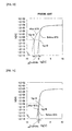
- FIG. 5 is shown a graph showing I-V characteristics of a prior-art pixel TFT substrate.
- FIG. 6 is shown a graph showing a relationship between gate-width and shifted voltage of hump according a pixel TFT substrate.
- FIG. 7 is shown a plane view, illustrating a prior-art structure according a side part of a pixel TFT substrate.
- FIG. 9 is shown a plane view, illustrating a structure according a side part of a pixel TFT substrate Embodiment 2.
- FIG. 10 is shown a graph showing I-V characteristics of a prior-art pixel TFT substrate.
- FIG. 11 is shown a graph showing I-V characteristics of a pixel TFT substrate Embodiment 1.
- FIG. 12 is shown a graph showing a relationship between projection part length and shifted voltage of hump according a pixel TFT substrate Embodiment 1.
- FIG. 13 is shown a graph showing a relationship between projection part width and shifted voltage of hump according a pixel TFT substrate Embodiment 1.
- TFT thin film transistor
- LCD liquid crystal display
- FIG. 1 is shown a schematic perspective view of an example of a liquid crystal display panel, which is used for a liquid crystal display device.
- a liquid crystal display panel having a pair of glass substrate, wherein an array substrate 2 and a counter substrate 3 . And a liquid crystal layer is sealed in between the array substrate 2 and the counter substrate 3 .
- Thin film transistors (TFTs) as pixel transistors formed on the array substrate 2 and there are driven as switching elements, and a picture is shown the display area 8 of the liquid crystal display panel.
- TFTs Thin film transistors
- a pixel electrodes are arranged on the array substrate 2 , and the pixel electrodes in a matrix form for correspond with an each image pixels. Scanning lines are formed along a column direction of the image pixels, and signal lines are formed along a rank direction of the image pixels. And above pixel transistors are formed on each junctions that crossing scanning lines and signal lines.
- driving circuit 4 for signal line, and driving circuit 5 for scanning line, and power circuit 6 , and other circuits.
- the peripheral circuit region 7 is so called frame area.
- the group of circuit 4 , 5 , 6 , and others is called peripheral circuit.
- the peripheral circuit is comprised plural thin film transistors (TFTs) and wiring together with circuit.
- TFTs thin film transistors
- a structure of thin film transistor substrate according to the present invention is used for the peripheral circuit in the peripheral circuit region 7 on the array substrate 2 .
- FIG. 2 is shown a cross-section view of an example of a pixel TFT substrate uses for the peripheral circuit as above described.
- the peripheral circuit is comprised plural thin film transistors (TFTs), and polycrystalline silicon thin film 13 as mean duties active layer of TFTs are formed on the array substrate 2 .
- the array substrate 2 is a glass substrate 11 that is coated by undercoat layer 12 , and the polycrystalline silicon thin film 13 is formed on the undercoat layer 12 , and the polycrystalline silicon thin film 13 as mean duties active layer of TFTs.
- the active layer is called a channel layer.
- the present invention is related the structure of FIG. 2 that is an example of a pixel TFT substrate.
- the undercoat layer 12 is formed on the glass substrate 11 as above described.
- the undercoat layer 12 coats a scratch or a pin-hole on the glass substrate 11 for surface flatting. And the undercoat layer 12 obstructs impurity diffusion for the polycrystalline silicon thin film 13 .
- the undercoat layer 12 is formed in a process of silicon oxide film, silicon nitride film, or as same thin film, for example. It is possible for additional flat layer that is formed fluid resin flowing by heat-treatment on the undercoat layer obstructs impurity diffusion. I.e. the undercoat layer 12 can be laminated layer. It is possible for omit the undercoat layer 12 when the glass substrate 11 has even flatness and few impurities.
- the polycrystalline silicon thin film 13 is formed in a procedure as below, for example. Anneal for an amorphous silicon (a-Si) film that is formed by plasma CVD. And polycrystalline for the amorphous silicon film by laser irradiation. The polycrystalline silicon thin film 13 is isolated each element as an island by etching. An example of shows FIG. 2 , the polycrystalline silicon thin film 13 is corresponds for an n-channel TFTs.
- Each polycrystalline silicon thin films 13 are formed a souse region 13 A and a drain region 13 B by impurity doping.
- LDD region as low-concentration impurity diffusion region 13 C, 13 D are formed each inside of the souse region 13 A and the drain region 13 B.
- FIG. 2 is shown a gate insulation layer 14 cover on the polycrystalline silicon thin film 13 as above described.
- a gate electrode 15 B is on the gate insulation layer 14 , and the gate electrode 15 B is overhead the channel of the polycrystalline silicon thin film 13 . So, the gate electrode 15 B is called a gate-channel.
- An interlayer dielectric 18 covers on the gate electrode 15 .
- a source electrode 16 is formed on the interlayer dielectric 18 , and a part of the source electrode 13 A is connected on the souse region 13 A through the interlayer dielectric 18 and the gate insulation layer 14 .
- a drain electrode 17 is formed on the interlayer dielectric 18 , and a part of the drain electrode 17 is connected on the drain region 13 B through the interlayer dielectric 18 and the gate insulation layer 14 .
- FIG. 3 is shown a plane view, illustrating a structure of a pixel TFT substrate Embodiment 1.
- the peripheral circuit is comprised plural thin film transistors (TFTs), and polycrystalline silicon thin film 13 as mean duties active layer of TFTs are formed on the array substrate 2 .
- the polycrystalline silicon thin film 13 is isolated each element as a given shape of island.
- the both sides of polycrystalline silicon thin films 13 are formed a souse region 13 A and a drain region 13 B by impurity doping.
- a gate electrode 15 is on the gate insulation layer 14 , and the gate electrode 15 is formed for along the overhead of the polycrystalline silicon thin film 13 .
- An interlayer dielectric 18 covers on the gate electrode 15 .
- a source electrode 16 is formed on the interlayer dielectric 18 , and a part of the source electrode 13 A is connected on the souse region 13 A through the interlayer dielectric 18 and the gate insulation layer 14 .
- a drain electrode 17 is formed on the interlayer dielectric 18 , and a part of the drain electrode 17 is connected on the drain region 13 B through the interlayer dielectric 18 and the gate insulation layer 14 .
- the channel of gate electrode 15 is located between the source electrode 16 and the drain electrode 17 .
- the source electrode 16 and the drain electrode 17 are located on both sides of the polycrystalline silicon thin films 13 .
- the gate electrode 15 is comprised a pair of projection part 15 A and a gate-channel 15 B.
- the gate-channel 15 B is formed for along the overhead of the polycrystalline silicon thin film 13 .
- the projection part 15 A is formed on both sides of the gate-channel 15 B, such as an alphabet-H structure show in FIG. 3 .
- a direction along the channel is called the channel-direction.
- the gate electrode 15 the width between the pair of projection part 15 A is named gate-width W, shown in FIG. 3 .
- the gate-width W is a width of the gate-channel 15 B.
- the length of the gate-channel 15 B for across the channel-direction is named gate-channel-length L, shown in FIG. 3 .
- a structure of thin film transistors (TFTs) according to the present invention is used for the peripheral circuit in the peripheral circuit region 7 on the array substrate 2 .
- the gate-width W is longer than the gate-channel-length L, as shown in FIG. 3 .
- the gate-width W is between 10 ⁇ m and 50 ⁇ m
- the gate-channel-length L is between 0.5 ⁇ m and 2.0 ⁇ m.
- the ratio as the gate-width W by gate-channel-length L (W/L) is at least 5 (W/L ⁇ 5).
- the pair of projection part 15 A is formed on both sides of the gate-channel 15 B, and a pair of pattern-edge lines 13 E is overlapped the pair of projection part 15 A, shown in FIG. 3 . Therefore, the hump level is reduced.
- the pair of projection part 15 A is formed on both sides of the gate-channel 15 B, such as an alphabet-H structure, and a pair of pattern-edge lines 13 E is covered the pair of projection part 15 A, shown in FIG. 3 . Therefore, the over current at the pair of pattern-edge lines 13 E is suppressed.
- the projection part 15 A is over the polycrystalline silicon thin film 13 for across the channel-direction, and the both side edges 13 A are covered by projection part 15 A, completely.
- the 15 A is consisting of Metal. Therefore, the over current at the pair of pattern-edge lines 13 E is suppressed and the hump level is reduced, well.
- the projection part 15 A is over the polycrystalline silicon thin film 13 for across the channel-direction, and the projection part 15 A is formed an inside position of the pair of pattern-edge lines 13 E at the polycrystalline silicon thin film 13 for along the channel-direction. It is also preferably Embodiment 2 as shown in FIG. 4 .
- the height of the pattern-edge is difference in level as inside.
- the gate leakage current is occurs between the gate electrode 15 and the pattern-edge of the polycrystalline silicon thin film 13 .
- the cross-line between the gate electrode 15 and the pattern-edge of the polycrystalline silicon thin film 13 is reduced. Therefore, the gate leakage current is reduced, well.
- the width D of projection part 15 A is shrinking. Therefore, parasitic capacitance is reduced.
- the Embodiment 2 can be narrow clearance of wiring position. Therefore, circuit integration is improved.
- TFT thin film transistor
- n-channel TFT As shown in FIG. 7 .
- Vg-B is the gate voltage before BTS
- Vg-A is the gate voltage after BTS, shown in FIG. 5 .
- Simulation cases are Prior art, Embodiment 1, and Embodiment 2.
- FIG. 7 is shown a plane view, illustrating a prior-art structure according a side part of a pixel TFT substrate. A route of edge-current is drawing as arrow direction shown in FIG. 7 .
- FIG. 8 is shown a plane view, illustrating a structure according a side part of a pixel TFT substrate Embodiment 1.
- Embodiment 1 has an alphabet-H structure of gate electrode and a pair of pattern-edge lines 13 E is overlapped the pair of projection part 15 A, and a route of edge-current is drawing as arrow direction shown in FIG. 8 .
- FIG. 9 is shown a plane view, illustrating a structure according a side part of a pixel TFT substrate Embodiment 2.
- Embodiment 2 has an alphabet-H structure of gate electrode and a projection part 15 A is formed an inside position of the pair of pattern-edge lines 13 E, and a route of edge-current is drawing as arrow shown in FIG. 8 .
- the edge-current at the polycrystalline silicon thin film 13 under fixed charge is simulated.
- the edge-current value for each an Embodiment 1 and an Embodiment 2 is a part per million based on edge-current value of a prior-art structure.
- FIG. 10 is shown a graph showing I-V characteristics of a prior-art pixel TFT substrate.
- FIG. 11 is shown a graph showing I-V characteristics of a pixel TFT substrate Embodiment 1.
- Vg-B is the gate voltage before BTS
- Vg-A is the gate voltage after BTS.
- 1nAVth is ⁇ 0.2 V as shown in FIG. 11 .
- 1nAVth is ⁇ 1.8 V as shown in FIG. 10 .
- the over current at the pair of pattern-edge lines 13 E is suppressed and the hump level is reduced, well.
- Embodiment 1 Evaluate hump characteristics according to Embodiment 1.
- FIG. 13 is shown a relationship graph between overlapped width TH and shifted voltage of hump 1nAVth according Embodiment 1. 1nAVth is approaching 0 V correlation with TH getting large as shown in FIG. 13 .
Landscapes
- Physics & Mathematics (AREA)
- Power Engineering (AREA)
- Engineering & Computer Science (AREA)
- Microelectronics & Electronic Packaging (AREA)
- General Physics & Mathematics (AREA)
- Condensed Matter Physics & Semiconductors (AREA)
- Computer Hardware Design (AREA)
- Nonlinear Science (AREA)
- Crystallography & Structural Chemistry (AREA)
- Optics & Photonics (AREA)
- Chemical & Material Sciences (AREA)
- Mathematical Physics (AREA)
- Ceramic Engineering (AREA)
- Liquid Crystal (AREA)
- Thin Film Transistor (AREA)
Abstract
Description
- [Patent document 1] JP3403807B2
Claims (8)
Applications Claiming Priority (2)
| Application Number | Priority Date | Filing Date | Title |
|---|---|---|---|
| JP2008-217278 | 2008-08-26 | ||
| JP2008217278A JP2010056169A (en) | 2008-08-26 | 2008-08-26 | Thin-film transistor and display using the same |
Publications (2)
| Publication Number | Publication Date |
|---|---|
| US20100110322A1 US20100110322A1 (en) | 2010-05-06 |
| US8085355B2 true US8085355B2 (en) | 2011-12-27 |
Family
ID=42071794
Family Applications (1)
| Application Number | Title | Priority Date | Filing Date |
|---|---|---|---|
| US12/547,340 Active 2030-04-08 US8085355B2 (en) | 2008-08-26 | 2009-08-25 | Structure of thin film transistors and liquid crystal display device having the same |
Country Status (2)
| Country | Link |
|---|---|
| US (1) | US8085355B2 (en) |
| JP (1) | JP2010056169A (en) |
Citations (2)
| Publication number | Priority date | Publication date | Assignee | Title |
|---|---|---|---|---|
| US6333520B1 (en) * | 1996-06-28 | 2001-12-25 | Seiko Epson Corporation | Thin film transistor, manufacturing method thereof, and circuit and liquid crystal display device using the thin film transistor |
| JP2008021760A (en) | 2006-07-12 | 2008-01-31 | Hitachi Displays Ltd | Thin film transistor and image display device |
Family Cites Families (4)
| Publication number | Priority date | Publication date | Assignee | Title |
|---|---|---|---|---|
| JPH08116063A (en) * | 1994-10-14 | 1996-05-07 | Sharp Corp | Thin-film transistor and liquid crystal display device |
| JP3520713B2 (en) * | 1997-03-26 | 2004-04-19 | セイコーエプソン株式会社 | Thin film transistor, liquid crystal display device and thin film transistor circuit using the same |
| JP2006128160A (en) * | 2004-10-26 | 2006-05-18 | Seiko Epson Corp | Semiconductor apparatus and its manufacturing method |
| KR101198127B1 (en) * | 2005-09-30 | 2012-11-12 | 엘지디스플레이 주식회사 | LCD and Method of fabricating of the same |
-
2008
- 2008-08-26 JP JP2008217278A patent/JP2010056169A/en active Pending
-
2009
- 2009-08-25 US US12/547,340 patent/US8085355B2/en active Active
Patent Citations (3)
| Publication number | Priority date | Publication date | Assignee | Title |
|---|---|---|---|---|
| US6333520B1 (en) * | 1996-06-28 | 2001-12-25 | Seiko Epson Corporation | Thin film transistor, manufacturing method thereof, and circuit and liquid crystal display device using the thin film transistor |
| JP2008021760A (en) | 2006-07-12 | 2008-01-31 | Hitachi Displays Ltd | Thin film transistor and image display device |
| US7755142B2 (en) * | 2006-07-12 | 2010-07-13 | Hitachi Displays, Ltd. | Thin-film transistor and image display device |
Also Published As
| Publication number | Publication date |
|---|---|
| US20100110322A1 (en) | 2010-05-06 |
| JP2010056169A (en) | 2010-03-11 |
Similar Documents
| Publication | Publication Date | Title |
|---|---|---|
| US6600197B1 (en) | Thin film transistor having a heat sink that exhibits a high degree of heat dissipation effect | |
| TW471180B (en) | Thin film transistor, its manufacturing method, circuit and liquid crystal display apparatus using thin film transistor | |
| US8330166B2 (en) | Thin-film semiconductor device for display apparatus thereof and manufacturing method thereof | |
| US6563136B2 (en) | Thin-film semiconductor device having a thin-film transistor for circuits that differs from a thin-film transistor for pixels | |
| TWI423448B (en) | System for displaying images | |
| US5703382A (en) | Array having multiple channel structures with continuously doped interchannel regions | |
| US6091115A (en) | Semiconductor device including a crystalline silicon film | |
| US9123820B2 (en) | Thin film transistor including semiconductor oxide layer having reduced resistance regions | |
| US20180219097A1 (en) | Semiconductor device and method for manufacturing same | |
| WO2021073253A1 (en) | Thin film transistor and manufacturing method therefor, array substrate, and display apparatus | |
| US7755142B2 (en) | Thin-film transistor and image display device | |
| US8748892B2 (en) | Thin film transistor and method for fabricating the same | |
| US7763889B2 (en) | Thin film transistor, method of fabricating the same, and a display device including the thin film transistor | |
| CN111276497A (en) | Driving backboard and display panel | |
| WO2016104253A1 (en) | Semiconductor device | |
| US10263016B2 (en) | Active matrix substrate and method for producing the same | |
| US8085355B2 (en) | Structure of thin film transistors and liquid crystal display device having the same | |
| CN216311789U (en) | Thin film transistor, array substrate, display panel and device | |
| JPH098314A (en) | Thin film transistor | |
| CN100481515C (en) | Unsymmetrical thin-film transistor structure | |
| US20070023836A1 (en) | Semiconductor device | |
| JP3321949B2 (en) | Thin film transistor and display device using the same | |
| JP4257482B2 (en) | THIN FILM TRANSISTOR, ITS MANUFACTURING METHOD, CIRCUIT USING THE SAME, AND LIQUID CRYSTAL DISPLAY DEVICE | |
| CN209912872U (en) | Novel oxide semiconductor narrow-frame display | |
| US8525176B2 (en) | Thin film transistor, display device using the same, and thin film transistor manufacturing method |
Legal Events
| Date | Code | Title | Description |
|---|---|---|---|
| AS | Assignment |
Owner name: TOSHIBA MOBILE DISPLAY CO., LTD.,JAPAN Free format text: ASSIGNMENT OF ASSIGNORS INTEREST;ASSIGNORS:WATAKABE, HAJIME;HIRAMATSU, MASATO;KIYOTA, TOSHIYA;AND OTHERS;REEL/FRAME:023491/0670 Effective date: 20091015 Owner name: TOSHIBA MOBILE DISPLAY CO., LTD., JAPAN Free format text: ASSIGNMENT OF ASSIGNORS INTEREST;ASSIGNORS:WATAKABE, HAJIME;HIRAMATSU, MASATO;KIYOTA, TOSHIYA;AND OTHERS;REEL/FRAME:023491/0670 Effective date: 20091015 |
|
| STCF | Information on status: patent grant |
Free format text: PATENTED CASE |
|
| AS | Assignment |
Owner name: JAPAN DISPLAY CENTRAL INC., JAPAN Free format text: CHANGE OF NAME;ASSIGNOR:TOSHIBA MOBILE DISPLAY CO., LTD.;REEL/FRAME:028339/0316 Effective date: 20120330 |
|
| FEPP | Fee payment procedure |
Free format text: PAYOR NUMBER ASSIGNED (ORIGINAL EVENT CODE: ASPN); ENTITY STATUS OF PATENT OWNER: LARGE ENTITY |
|
| FPAY | Fee payment |
Year of fee payment: 4 |
|
| MAFP | Maintenance fee payment |
Free format text: PAYMENT OF MAINTENANCE FEE, 8TH YEAR, LARGE ENTITY (ORIGINAL EVENT CODE: M1552); ENTITY STATUS OF PATENT OWNER: LARGE ENTITY Year of fee payment: 8 |
|
| MAFP | Maintenance fee payment |
Free format text: PAYMENT OF MAINTENANCE FEE, 12TH YEAR, LARGE ENTITY (ORIGINAL EVENT CODE: M1553); ENTITY STATUS OF PATENT OWNER: LARGE ENTITY Year of fee payment: 12 |