US8084732B2 - Resistive glass structures used to shape electric fields in analytical instruments - Google Patents
Resistive glass structures used to shape electric fields in analytical instruments Download PDFInfo
- Publication number
- US8084732B2 US8084732B2 US12/644,078 US64407809A US8084732B2 US 8084732 B2 US8084732 B2 US 8084732B2 US 64407809 A US64407809 A US 64407809A US 8084732 B2 US8084732 B2 US 8084732B2
- Authority
- US
- United States
- Prior art keywords
- tube
- length
- glass tube
- along
- electrical resistance
- Prior art date
- Legal status (The legal status is an assumption and is not a legal conclusion. Google has not performed a legal analysis and makes no representation as to the accuracy of the status listed.)
- Active, expires
Links
Images


Classifications
-
- H—ELECTRICITY
- H01—ELECTRIC ELEMENTS
- H01J—ELECTRIC DISCHARGE TUBES OR DISCHARGE LAMPS
- H01J49/00—Particle spectrometers or separator tubes
- H01J49/26—Mass spectrometers or separator tubes
- H01J49/34—Dynamic spectrometers
- H01J49/40—Time-of-flight spectrometers
- H01J49/405—Time-of-flight spectrometers characterised by the reflectron, e.g. curved field, electrode shapes
-
- C—CHEMISTRY; METALLURGY
- C03—GLASS; MINERAL OR SLAG WOOL
- C03C—CHEMICAL COMPOSITION OF GLASSES, GLAZES OR VITREOUS ENAMELS; SURFACE TREATMENT OF GLASS; SURFACE TREATMENT OF FIBRES OR FILAMENTS MADE FROM GLASS, MINERALS OR SLAGS; JOINING GLASS TO GLASS OR OTHER MATERIALS
- C03C17/00—Surface treatment of glass, not in the form of fibres or filaments, by coating
- C03C17/22—Surface treatment of glass, not in the form of fibres or filaments, by coating with other inorganic material
- C03C17/23—Oxides
-
- C—CHEMISTRY; METALLURGY
- C03—GLASS; MINERAL OR SLAG WOOL
- C03C—CHEMICAL COMPOSITION OF GLASSES, GLAZES OR VITREOUS ENAMELS; SURFACE TREATMENT OF GLASS; SURFACE TREATMENT OF FIBRES OR FILAMENTS MADE FROM GLASS, MINERALS OR SLAGS; JOINING GLASS TO GLASS OR OTHER MATERIALS
- C03C23/00—Other surface treatment of glass not in the form of fibres or filaments
- C03C23/008—Other surface treatment of glass not in the form of fibres or filaments comprising a lixiviation step
-
- C—CHEMISTRY; METALLURGY
- C03—GLASS; MINERAL OR SLAG WOOL
- C03C—CHEMICAL COMPOSITION OF GLASSES, GLAZES OR VITREOUS ENAMELS; SURFACE TREATMENT OF GLASS; SURFACE TREATMENT OF FIBRES OR FILAMENTS MADE FROM GLASS, MINERALS OR SLAGS; JOINING GLASS TO GLASS OR OTHER MATERIALS
- C03C4/00—Compositions for glass with special properties
- C03C4/14—Compositions for glass with special properties for electro-conductive glass
-
- C—CHEMISTRY; METALLURGY
- C03—GLASS; MINERAL OR SLAG WOOL
- C03C—CHEMICAL COMPOSITION OF GLASSES, GLAZES OR VITREOUS ENAMELS; SURFACE TREATMENT OF GLASS; SURFACE TREATMENT OF FIBRES OR FILAMENTS MADE FROM GLASS, MINERALS OR SLAGS; JOINING GLASS TO GLASS OR OTHER MATERIALS
- C03C2217/00—Coatings on glass
- C03C2217/20—Materials for coating a single layer on glass
- C03C2217/21—Oxides
- C03C2217/228—Other specific oxides
-
- C—CHEMISTRY; METALLURGY
- C03—GLASS; MINERAL OR SLAG WOOL
- C03C—CHEMICAL COMPOSITION OF GLASSES, GLAZES OR VITREOUS ENAMELS; SURFACE TREATMENT OF GLASS; SURFACE TREATMENT OF FIBRES OR FILAMENTS MADE FROM GLASS, MINERALS OR SLAGS; JOINING GLASS TO GLASS OR OTHER MATERIALS
- C03C2217/00—Coatings on glass
- C03C2217/90—Other aspects of coatings
- C03C2217/91—Coatings containing at least one layer having a composition gradient through its thickness
-
- C—CHEMISTRY; METALLURGY
- C03—GLASS; MINERAL OR SLAG WOOL
- C03C—CHEMICAL COMPOSITION OF GLASSES, GLAZES OR VITREOUS ENAMELS; SURFACE TREATMENT OF GLASS; SURFACE TREATMENT OF FIBRES OR FILAMENTS MADE FROM GLASS, MINERALS OR SLAGS; JOINING GLASS TO GLASS OR OTHER MATERIALS
- C03C2218/00—Methods for coating glass
- C03C2218/30—Aspects of methods for coating glass not covered above
- C03C2218/34—Masking
-
- C—CHEMISTRY; METALLURGY
- C03—GLASS; MINERAL OR SLAG WOOL
- C03C—CHEMICAL COMPOSITION OF GLASSES, GLAZES OR VITREOUS ENAMELS; SURFACE TREATMENT OF GLASS; SURFACE TREATMENT OF FIBRES OR FILAMENTS MADE FROM GLASS, MINERALS OR SLAGS; JOINING GLASS TO GLASS OR OTHER MATERIALS
- C03C2218/00—Methods for coating glass
- C03C2218/30—Aspects of methods for coating glass not covered above
- C03C2218/35—Exuding
Definitions
- This invention relates generally to mass spectrometers, and in particular to a reflectron type time-of-flight mass spectrometer and to a glass reflectron lens for such a spectrometer wherein the lens has a gradient electrical resistance on its surface.
- Mass spectrometers are analytical instruments capable of identifying unknown materials in complex mixtures with precision in the parts per billion range. Once used exclusively in research laboratories, mass spectrometers are now in use in a broad range of applications. They are used in screening for pesticides in canned foods, controlling semiconductor manufacturing processes, diagnosing disease, exploring for natural resources, discovering new pharmaceuticals, predicting volcano eruptions, and security systems. Indeed, these instruments have traveled beyond our world aboard the Galileo and Cassini spacecrafts to provide atmospheric analysis of neighboring worlds within our solar system.
- Time of Flight Mass Spectrometry is rapidly becoming the most popular method of mass separation in analytical chemistry.
- the development of low cost digitizers and extremely fast ion detectors has fueled this popularity.
- TOF-MS is easily deployed and can produce very high mass resolution.
- This technique of mass separation can be adapted for many forms of sample introduction and ionization.
- time of flight mass analyzers perform well with very high mass molecules of the type frequently found in protean applications. Wiley and McLaren in 1955, followed by Cotter in 1992, and Wollnik in 1993 have described time of flight mass analyzers.
- Time-of-flight mass spectrometers are produced in two main types: linear instruments and reflectron instruments.
- FIG. 1 illustrates a linear time of flight mass spectrometer embodied as a matrix assisted laser desorption ionization (MALDI) instrument 100 .
- MALDI matrix assisted laser desorption ionization
- Equation 1 m/z ( d 2 /2 V se )
- Equation 1 m/z is the mass to charge ratio of the ion, d is the distance to the detector, and V se is the acceleration potential.
- the lighter ions (i.e. ions having relatively lower masses) travel toward the detector 108 faster than the higher mass ions. If the flight tube is long enough, the ions will arrive at the detector according to their mass, i.e., lowest to highest.
- FIG. 2 illustrates the arrival time spectrum of a sample of Brandykinin analyzed on a linear time of flight mass spectrometer. Knowing the exact arrival times, Equation 1 can be used to solve for the mass-to-charge ratios of the ions.
- the second type of time-of-flight mass spectrometer is the reflectron instrument.
- FIG. 3 illustrates a known arrangement of a reflectron TOF mass spectrometer 300 .
- the reflectron design takes advantage of the fact that the further the ions are allowed to travel, the greater the distance between ions of slightly differing masses. Greater distances between ions with different masses will increase the arrival time differences between the ions and thereby increase the resolution at which ions having similar mass-to-charge ratios (m/z) can be differentiated.
- the reflectron design corrects for the energy dispersion of the ions leaving the source.
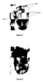
- FIG. 4 shows the construction of a known reflectron lens. It consists of a plurality of stacked metal rings that are spaced and insulated from each other. An electrostatic field is created within the reflectron lens 304 by applying different high voltage potentials to each of the metal rings. The electrostatic field has a polarity that causes the ions to decelerate and eventually reverse their direction. The ions exit the lens 304 and are directed to the ion detector 306 . The action of the reflectron lens on the ions effectively doubles their length of travel in the flight tube. The additional travel time improves mass resolution without adding additional length to the flight tube.
- a reflectron lens consists of a stack of precision ground metal rings 402 alternating with insulating spacers 404 . The rings and spacers are held together with threaded rods 406 .
- the reflectron lens assembly may have hundreds of components which must be carefully assembled and aligned (typically by hand) in a clean, dust free environment. Additionally, a voltage divider must be included in each row or layer in order to produce the electrostatic field gradient necessary to reverse the direction of the ions.
- An improved variant of the classical reflectron lens design utilizes a single resistive glass tube to generate the gradient electric field.
- a resistive glass tube reflectron lens is shown in FIG. 5 .
- the monolithic structure of the resistive glass tube replaces the multi-component assembly of the metal ring type of reflectron lens.
- Reflectron lenses fabricated from resistive glass tubes have thus far been produced with a uniform resistance along the inside of the tube. That architecture is useful for many reflectron geometries. However, a significant performance advantage and greater design flexibility could be realized if the electrical resistance varied discretely or continuously along the length of the lens.
- Resistive glass reflectron lenses are fabricated from lead silicate glass that has been subjected to a hydrogen reduction process to produce a thin resistive layer on the inside surface of the tube.
- a resistive glass reflectron lens is described in U.S. Pat. No. 7,154,086, the entire disclosure of which is incorporated herein by reference.
- the hydrogen reduction process consists of loading the glass tube into a closed furnace through which pure hydrogen or a controlled mixture of hydrogen and oxygen is purged.
- the temperature is gradually increased, typically at a rate of 1-3 degrees per minute.
- a chemical reaction occurs in the glass in which the lead oxide in the glass converts to a semi-conductive state. This reaction occurs in the first few hundred angstroms of the cross section of the glass.
- Temperature, time, gas pressure, and gas flow can be controlled to provide a desired amount of electrical resistance on the surface of the glass.
- the electrical resistance is also dependent on the composition of the glass.
- a glass containing more lead oxide with a modifier such as bismuth can be used to produce lower resistances.
- the hydrogen reduction process makes all surfaces of the glass tube conductive. Unwanted conductive surfaces can be stripped by chemical or mechanical means.
- a known hydrogen reduction process has the following parameters:
- the reduction temperature is limited on the low end by the minimum temperature needed to sustain the reaction and is limited on the high side by the sag point of the glass.
- a segmented resistive tube in which certain sections of the tube have significantly different values of electrical resistance.
- the variation may be linear or nonlinear.
- an orthogonal geometry time of flight mass spectrometer utilizes a reflectron tube having a nonlinear resistance characteristic.
- U.S. Pat. No. 7,081,618, the entire disclosure of which is incorporated herein by reference, and U.S. Pat. No. 7,154,086 describe methods to produce a uniform electrical resistance in a lead silicate glass tube by subjecting the tube to a reducing environment within a hydrogen furnace.
- a reflectron lens for a time-of-flight mass spectrometer that includes a glass tube having a conductive surface along the length of the tube.
- the conductive surface has an electrical resistance gradient along its length.
- the electrical resistance gradient provides an electric field interior to the tube that varies in strength along the length of the tube when an electric potential is applied to opposing ends of the tube.
- a time-of-flight mass spectrometer that has a reflectron lens.
- the reflectron lens is formed of a glass tube having a conductive surface along the length of the tube.
- the conductive surface has an electrical resistance gradient along its length.
- the time-of-flight mass spectrometer according to this invention also includes a voltage supply electrically connected to opposite ends of the tube.
- a method of preparing a glass tube for use as a reflectron lens includes the steps of providing a glass tube wherein the glass contains a lead compound and immersing a portion of the glass tube in an acidic solution.
- the portion of the glass tube is held in the acidic solution for a time sufficient to remove lead from the surface of the immersed portion of said glass tube.
- the surface of the glass tube is then chemically reduced to form an electrically resistive layer on the surface of the glass tube. In this manner, the electrical resistance of the portion held in the acidic solution will be lower than the electrical resistance of another portion of the glass tube.
- FIG. 1 is a schematic diagram of a linear time-of-flight mass spectrometer
- FIG. 2 is a graph of the response of a linear time-of-flight mass spectrometer for a sample of Brandykinin
- FIG. 3 is a schematic diagram of a reflectron type mass spectrometer
- FIG. 4 is a photograph of a metal-ring reflectron lens
- FIG. 5 is a photograph of a glass reflectron lens
- FIG. 6 is a schematic diagram of an apparatus for carrying out selective leaching of lead from a lead silicate glass tube in accordance with the present invention
- FIG. 7 is a schematic diagram showing the step of selective immersion of a glass tube in a lead leaching solution
- FIG. 8 is a graph of the electrical resistance per unit area of a glass tube prepared in accordance with the present invention wherein the electrical resistance varies in steps;
- FIG. 9 is a graph of the electrical resistance per unit area of a glass tube prepared in accordance with the present invention wherein the electrical resistance varies linearly;
- FIG. 10 is a graph of the electrical resistance per unit area of a glass tube prepared in accordance with the present invention wherein the electrical resistance varies nonlinearly;
- FIG. 11 is a schematic diagram of a reflectron type mass spectrometer utilizing a glass reflectron lens made in accordance with the present invention.
- the lead oxide within lead silicate bulk glass is reacted with hydrogen at temperatures ranging from 350-550° C.
- the chemical reaction occurs on the surface of the work piece, not in the interior of the bulk material.
- the chemical reaction proceeds as follows: Pb 2 O 5 +H 2 ⁇ Pb 2 O x +H 2 O
- the reaction yields a semi-conductive form of lead oxide that is uniformly distributed over all surfaces of the work piece.
- the electrical resistance along the surface is a function of the process parameters of temperature, time, the pressure and composition of the hydrogen/oxygen cover gas, and the composition of the lead silicate glass at the reduction surface.
- One method to change the composition of the glass structure over small distances would be to preferentially remove lead from the surface of the substrate. Preferentially removing lead from the immediate surface in the desired locations would cause those areas to have higher resistances because less lead would be reduced to the semi-conducting form of the lead oxide during the hydrogen reduction process.
- Lead can be preferentially removed from the surface of a lead silicate glass in a leaching process by exposing the workpiece to certain acidic solutions.
- Experiments have been performed which indicate that the resistance obtained after the reduction process is inversely proportional to the exposure time to the leachant for a given concentration and temperature of the solution.
- FIG. 6 illustrates such a device.
- the preferred machine 600 includes an acid tank 602 which holds the acidic solution used for leaching.
- the work piece 604 is held by a chuck 606 that is attached to a slide mechanism 608 .
- the slide 608 is moved by rotation of a lead screw (not shown).
- An L-shaped support fixture 610 is attached to the slide 608 .
- the chuck 606 is supported from the fixture 610 with a gimbal 612 .
- the slide mechanism 608 is supported by a mounting bracket 614 that is mounted on a table 616 or other support stand.
- a shield 618 is provided to protect the slide mechanism 608 .
- the slide mechanism 608 is connected to a DC stepper motor 620 that is mounted to the table 616 .
- the stepper motor 620 has a drive shaft to which a drive pulley 624 is attached.
- a second drive pulley 628 mounted on a drive shaft 630 that is connected to the lead screw in the slide mechanism 608 .
- a timing belt 626 connects the first drive pulley 624 to the second drive pulley 628 such that rotation of the stepper motor shaft results in rotation of the drive shaft 630 .
- the drive shaft 630 is coupled to the lead screw with a flexible connector 634 to complete the linkage between the stepper motor 620 and the lead screw. With the arrangement shown in FIG. 6 , the glass tube work piece 604 can be precisely moved into and out of the acid tank 602 to permit selective leaching of the lead from the glass.
- a step-wise resistance gradient is produced by stopping the immersion of the glass tube at a predetermined location along the length of the tube.
- the tube is held for a time sufficient to achieve a predefined amount of leaching.
- the resistance of the portion of the tube immersed in the solution is significantly higher than the portion not exposed to the solution.
- FIG. 8 illustrates the stepped resistance profile along the length of the glass tube. Please note the y-scale is resistance per unit area, not total end-to-point resistance along the wall of the tube.
- the apparatus shown in FIG. 6 can be used to slowly lower the work piece into the acid solution at a controlled rate of speed. Lowering the piece at a fixed rate creates a linear resistance profile as illustrated in FIG. 9 .
- the apparatus shown in FIG. 6 is modulated to perform a process in which a combination of the steps described above is performed. For example, a first portion of the glass tube is exposed for a first time period, while a different section is moved continuously as it is exposed, and a third section is not exposed at all.
- FIG. 10 illustrates the nonlinear resistance profile produced by such a process. In this manner, an unlimited number of resistance profiles can be produced.
- Glass tubes having low resistances in the middle portion of the tube length can be produced either by masking the work piece in the area of desired low resistance or flipping the work piece in the holder.
- Masking materials can be applied by brushing, spraying, taping, or they can be spun on.
- a glass tube made in accordance with the present invention can be used a reflectron lens in a reflectron type mass spectrometer. Such an arrangement is shown in FIG. 11 .
- An ion mass spectrometer 1100 according to the present invention has a flight tube 1102 through which the ions travel.
- the mass spectrometer 1100 includes a reflectron lens 1104 that is formed from a glass tube having a gradient electrical resistance along the length of its surface.
- the reflectron lens 1104 is disposed at an end of the flight tube 1102 distal from an ion detector 1108 .
- the ion detector 1108 is a microchannel plate-based ion detector.
- a linear detector may be provided at the reflectron lens end of the flight tube 1102 .
- An ionization section 1110 is provided at the same end of the flight tube 1102 as the ion detector 1108 , although spaced therefrom. The ionization section 1110 provides ionized sample material into the flight tube 1102
Abstract
Description
t 2 =m/z(d 2/2V se)
In
Pb2O5+H2→Pb2Ox+H2O
The reaction yields a semi-conductive form of lead oxide that is uniformly distributed over all surfaces of the work piece. The electrical resistance along the surface is a function of the process parameters of temperature, time, the pressure and composition of the hydrogen/oxygen cover gas, and the composition of the lead silicate glass at the reduction surface.
Claims (21)
Priority Applications (1)
| Application Number | Priority Date | Filing Date | Title |
|---|---|---|---|
| US12/644,078 US8084732B2 (en) | 2006-03-10 | 2009-12-22 | Resistive glass structures used to shape electric fields in analytical instruments |
Applications Claiming Priority (3)
| Application Number | Priority Date | Filing Date | Title |
|---|---|---|---|
| US78108806P | 2006-03-10 | 2006-03-10 | |
| US11/683,713 US20080073516A1 (en) | 2006-03-10 | 2007-03-08 | Resistive glass structures used to shape electric fields in analytical instruments |
| US12/644,078 US8084732B2 (en) | 2006-03-10 | 2009-12-22 | Resistive glass structures used to shape electric fields in analytical instruments |
Related Parent Applications (1)
| Application Number | Title | Priority Date | Filing Date |
|---|---|---|---|
| US11/683,713 Continuation US20080073516A1 (en) | 2006-03-10 | 2007-03-08 | Resistive glass structures used to shape electric fields in analytical instruments |
Publications (2)
| Publication Number | Publication Date |
|---|---|
| US20100090098A1 US20100090098A1 (en) | 2010-04-15 |
| US8084732B2 true US8084732B2 (en) | 2011-12-27 |
Family
ID=38288453
Family Applications (2)
| Application Number | Title | Priority Date | Filing Date |
|---|---|---|---|
| US11/683,713 Abandoned US20080073516A1 (en) | 2006-03-10 | 2007-03-08 | Resistive glass structures used to shape electric fields in analytical instruments |
| US12/644,078 Active 2027-04-29 US8084732B2 (en) | 2006-03-10 | 2009-12-22 | Resistive glass structures used to shape electric fields in analytical instruments |
Family Applications Before (1)
| Application Number | Title | Priority Date | Filing Date |
|---|---|---|---|
| US11/683,713 Abandoned US20080073516A1 (en) | 2006-03-10 | 2007-03-08 | Resistive glass structures used to shape electric fields in analytical instruments |
Country Status (5)
| Country | Link |
|---|---|
| US (2) | US20080073516A1 (en) |
| EP (1) | EP1833076B1 (en) |
| JP (1) | JP5382485B2 (en) |
| CA (1) | CA2581463C (en) |
| IL (1) | IL181836A (en) |
Cited By (3)
| Publication number | Priority date | Publication date | Assignee | Title |
|---|---|---|---|---|
| US8841609B2 (en) | 2012-10-26 | 2014-09-23 | Autoclear LLC | Detection apparatus and methods utilizing ion mobility spectrometry |
| DE102014119446A1 (en) | 2013-12-24 | 2015-06-25 | Waters Technologies Corporation | Ion-optical element |
| US10192725B2 (en) | 2013-12-24 | 2019-01-29 | Waters Technologies Corporation | Atmospheric interface for electrically grounded electrospray |
Families Citing this family (6)
| Publication number | Priority date | Publication date | Assignee | Title |
|---|---|---|---|---|
| US20080073516A1 (en) * | 2006-03-10 | 2008-03-27 | Laprade Bruce N | Resistive glass structures used to shape electric fields in analytical instruments |
| US8704173B2 (en) * | 2009-10-14 | 2014-04-22 | Bruker Daltonik Gmbh | Ion cyclotron resonance measuring cells with harmonic trapping potential |
| US8410442B2 (en) | 2010-10-05 | 2013-04-02 | Nathaniel S. Hankel | Detector tube stack with integrated electron scrub system and method of manufacturing the same |
| FR2971360B1 (en) * | 2011-02-07 | 2014-05-16 | Commissariat Energie Atomique | MICRO-REFLECTRON FOR TIME-OF-FLIGHT MASS SPECTROMETER |
| EP3005402B1 (en) * | 2013-05-31 | 2021-08-18 | PerkinElmer Health Sciences, Inc. | Time of flight tubes and methods of using them |
| JP6624790B2 (en) | 2014-03-03 | 2019-12-25 | キヤノン株式会社 | Projection type charged particle optical system and imaging mass spectrometer |
Citations (78)
| Publication number | Priority date | Publication date | Assignee | Title |
|---|---|---|---|---|
| US2680826A (en) * | 1948-05-01 | 1954-06-08 | Sylvania Electric Prod | Stabilized klystron |
| US2841729A (en) | 1955-09-01 | 1958-07-01 | Bendix Aviat Corp | Magnetic electron multiplier |
| US2841879A (en) | 1957-01-07 | 1958-07-08 | Lanski Harry | Layout guide clamp |
| US3197663A (en) | 1962-06-04 | 1965-07-27 | Bendix Corp | Electron multiplier gate |
| US3424909A (en) | 1965-03-24 | 1969-01-28 | Csf | Straight parallel channel electron multipliers |
| US3488509A (en) | 1964-12-07 | 1970-01-06 | Bendix Corp | Particle acceleration having low electron gain |
| US3519870A (en) | 1967-05-18 | 1970-07-07 | Xerox Corp | Spiraled strip material having parallel grooves forming plurality of electron multiplier channels |
| US3634712A (en) | 1970-03-16 | 1972-01-11 | Itt | Channel-type electron multiplier for use with display device |
| US3673449A (en) | 1969-04-04 | 1972-06-27 | Philips Corp | Channel amplifying device comprising a plurality of coupled channel plates |
| US3675063A (en) | 1970-01-02 | 1972-07-04 | Stanford Research Inst | High current continuous dynode electron multiplier |
| US3819941A (en) * | 1973-10-15 | 1974-06-25 | Bendix Corp | Mass dependent ion microscope having an array of small mass filters |
| US3885180A (en) | 1973-07-10 | 1975-05-20 | Us Army | Microchannel imaging display device |
| US3902089A (en) | 1971-07-08 | 1975-08-26 | Philips Corp | Channel plate matrix of tubes having twisted septa |
| US3911167A (en) | 1970-05-01 | 1975-10-07 | Texas Instruments Inc | Electron multiplier and method of making same |
| US3959038A (en) | 1975-04-30 | 1976-05-25 | The United States Of America As Represented By The Secretary Of The Army | Electron emitter and method of fabrication |
| US3976905A (en) | 1973-07-05 | 1976-08-24 | Ramot University For Applied Research And Industrial Development Ltd. | Channel electron multipliers |
| US3996474A (en) * | 1967-01-04 | 1976-12-07 | Purification Sciences, Inc. | Corona generator apparatus |
| US4015159A (en) | 1975-09-15 | 1977-03-29 | Bell Telephone Laboratories, Incorporated | Semiconductor integrated circuit transistor detector array for channel electron multiplier |
| US4051403A (en) | 1976-08-10 | 1977-09-27 | The United States Of America As Represented By The Secretary Of The Army | Channel plate multiplier having higher secondary emission coefficient near input |
| US4073989A (en) | 1964-01-17 | 1978-02-14 | Horizons Incorporated | Continuous channel electron beam multiplier |
| US4093562A (en) | 1976-02-20 | 1978-06-06 | Matsushita Electric Industrial Co., Ltd. | Polymeric compositions for manufacture of secondary electron multiplier tubes and method for manufacture thereof |
| US4095136A (en) | 1971-10-28 | 1978-06-13 | Varian Associates, Inc. | Image tube employing a microchannel electron multiplier |
| US4099079A (en) | 1975-10-30 | 1978-07-04 | U.S. Philips Corporation | Secondary-emissive layers |
| US4126781A (en) * | 1977-05-10 | 1978-11-21 | Extranuclear Laboratories, Inc. | Method and apparatus for producing electrostatic fields by surface currents on resistive materials with applications to charged particle optics and energy analysis |
| US4217489A (en) | 1977-08-05 | 1980-08-12 | U.S. Philips Corporation | Device for location-sensitive detection of photon and/or particle radiation |
| US4236073A (en) | 1977-05-27 | 1980-11-25 | Martin Frederick W | Scanning ion microscope |
| US4267442A (en) | 1978-08-21 | 1981-05-12 | U.S. Philips Corporation | Electron multiplier device comprising microchannel plates with optical feedback suppression for image intensifier tubes |
| CA1121858A (en) | 1978-10-13 | 1982-04-13 | Jean-Denis Carette | Electron multiplier device |
| US4352985A (en) | 1974-01-08 | 1982-10-05 | Martin Frederick W | Scanning ion microscope |
| US4390784A (en) * | 1979-10-01 | 1983-06-28 | The Bendix Corporation | One piece ion accelerator for ion mobility detector cells |
| US4454422A (en) | 1982-01-27 | 1984-06-12 | Siemens Gammasonics, Inc. | Radiation detector assembly for generating a two-dimensional image |
| US4468420A (en) | 1983-07-14 | 1984-08-28 | Nippon Sheet Glass Co., Ltd. | Method for making a silicon dioxide coating |
| USRE31847E (en) | 1973-01-02 | 1985-03-12 | Eastman Kodak Company | Apparatus and method for producing images corresponding to patterns of high energy radiation |
| US4558144A (en) | 1984-10-19 | 1985-12-10 | Corning Glass Works | Volatile metal complexes |
| US4563250A (en) | 1984-03-10 | 1986-01-07 | Kernforschungszentrum Karlsruhe Gmbh | Method for producing multichannel plates |
| US4577133A (en) | 1983-10-27 | 1986-03-18 | Wilson Ronald E | Flat panel display and method of manufacture |
| US4589952A (en) | 1982-07-03 | 1986-05-20 | International Business Machines Corporation | Method of making trenches with substantially vertical sidewalls in silicon through reactive ion etching |
| US4598037A (en) * | 1984-12-21 | 1986-07-01 | E. I. Du Pont De Nemours And Company | Photosensitive conductive metal composition |
| US4624739A (en) | 1985-08-09 | 1986-11-25 | International Business Machines Corporation | Process using dry etchant to avoid mask-and-etch cycle |
| US4624736A (en) | 1984-07-24 | 1986-11-25 | The United States Of America As Represented By The United States Department Of Energy | Laser/plasma chemical processing of substrates |
| GB2180986A (en) | 1985-09-25 | 1987-04-08 | English Electric Valve Co Ltd | Image intensifier |
| US4659429A (en) | 1983-08-03 | 1987-04-21 | Cornell Research Foundation, Inc. | Method and apparatus for production and use of nanometer scale light beams |
| JPS62119121A (en) | 1985-11-18 | 1987-05-30 | Hitachi Cable Ltd | Production of vitreous body having refractive index distribution |
| US4693781A (en) | 1986-06-26 | 1987-09-15 | Motorola, Inc. | Trench formation process |
| US4698129A (en) | 1986-05-01 | 1987-10-06 | Oregon Graduate Center | Focused ion beam micromachining of optical surfaces in materials |
| US4707218A (en) | 1986-10-28 | 1987-11-17 | International Business Machines Corporation | Lithographic image size reduction |
| US4714861A (en) | 1986-10-01 | 1987-12-22 | Galileo Electro-Optics Corp. | Higher frequency microchannel plate |
| US4725332A (en) | 1983-10-13 | 1988-02-16 | Gesellschaft Fur Schwerionenforschung Mbh | Method for monitoring microhole growth during production of microholes having a predetermined diameter |
| US4731559A (en) | 1986-06-03 | 1988-03-15 | U.S. Philips Corporation | Electron multiplier plate with controlled multiplication |
| US4734158A (en) | 1987-03-16 | 1988-03-29 | Hughes Aircraft Company | Molecular beam etching system and method |
| US4740267A (en) | 1987-02-20 | 1988-04-26 | Hughes Aircraft Company | Energy intensive surface reactions using a cluster beam |
| US4764245A (en) | 1986-05-07 | 1988-08-16 | Siemens Aktiengesellschaft | Method for generating contact holes with beveled sidewalls in intermediate oxide layers |
| US4780395A (en) | 1986-01-25 | 1988-10-25 | Kabushiki Kaisha Toshiba | Microchannel plate and a method for manufacturing the same |
| US4786361A (en) | 1986-03-05 | 1988-11-22 | Kabushiki Kaisha Toshiba | Dry etching process |
| US4790903A (en) | 1986-04-28 | 1988-12-13 | University Of Tokyo | Intermittent etching process |
| US4794296A (en) | 1986-03-18 | 1988-12-27 | Optron System, Inc. | Charge transfer signal processor |
| US4800263A (en) | 1987-02-17 | 1989-01-24 | Optron Systems, Inc. | Completely cross-talk free high spatial resolution 2D bistable light modulation |
| US4802951A (en) | 1986-03-07 | 1989-02-07 | Trustees Of Boston University | Method for parallel fabrication of nanometer scale multi-device structures |
| US4806827A (en) | 1985-12-31 | 1989-02-21 | U.S. Philips Corporation | Multiplier element of the aperture plate type, and method of manufacture |
| US4825118A (en) | 1985-09-06 | 1989-04-25 | Hamamatsu Photonics Kabushiki Kaisha | Electron multiplier device |
| US5086248A (en) | 1989-08-18 | 1992-02-04 | Galileo Electro-Optics Corporation | Microchannel electron multipliers |
| US5109157A (en) * | 1991-03-21 | 1992-04-28 | Loen Andrew E | Ion mobility detector |
| US5162649A (en) * | 1988-04-06 | 1992-11-10 | Graseby Ionics Ltd. | Ion mobility detector |
| US5205902A (en) | 1989-08-18 | 1993-04-27 | Galileo Electro-Optics Corporation | Method of manufacturing microchannel electron multipliers |
| US5351332A (en) | 1992-03-18 | 1994-09-27 | Galileo Electro-Optics Corporation | Waveguide arrays and method for contrast enhancement |
| US5378960A (en) | 1989-08-18 | 1995-01-03 | Galileo Electro-Optics Corporation | Thin film continuous dynodes for electron multiplication |
| EP0704879A1 (en) | 1994-09-30 | 1996-04-03 | Hewlett-Packard Company | Charged particle mirror |
| US5834771A (en) * | 1994-07-08 | 1998-11-10 | Agency For Defence Development | Ion mobility spectrometer utilizing flexible printed circuit board and method for manufacturing thereof |
| US6008491A (en) | 1997-10-15 | 1999-12-28 | The United States Of America As Represented By The United States Department Of Energy | Time-of-flight SIMS/MSRI reflectron mass analyzer and method |
| US6369383B1 (en) | 1999-08-16 | 2002-04-09 | The John Hopkins University | Flexboard reflector |
| US20030230726A1 (en) * | 2002-02-26 | 2003-12-18 | Van Der Veer Wytze E. | Apparatus and method for using a volume conductive electrode with ion optical elements for a time-of-flight mass spectrometer |
| US6717135B2 (en) | 2001-10-12 | 2004-04-06 | Agilent Technologies, Inc. | Ion mirror for time-of-flight mass spectrometer |
| US20040183028A1 (en) * | 2003-03-19 | 2004-09-23 | Bruce Laprade | Conductive tube for use as a reflectron lens |
| US6825474B2 (en) | 2002-02-07 | 2004-11-30 | Agilent Technologies, Inc. | Dimensionally stable ion optic component and method of manufacturing |
| US20050109930A1 (en) * | 2003-10-14 | 2005-05-26 | Hill Herbert H.Jr. | Ion mobility spectrometry method and apparatus |
| US7141787B2 (en) * | 2004-05-17 | 2006-11-28 | Burle Technologies, Inc. | Detector for a co-axial bipolar time-of-flight mass spectrometer |
| US20080073516A1 (en) * | 2006-03-10 | 2008-03-27 | Laprade Bruce N | Resistive glass structures used to shape electric fields in analytical instruments |
| US20080173809A1 (en) * | 2006-07-11 | 2008-07-24 | Excellims Corporation | Methods and apparatus for the ion mobility based separation and collection of molecules |
Family Cites Families (6)
| Publication number | Priority date | Publication date | Assignee | Title |
|---|---|---|---|---|
| DK0458713T3 (en) * | 1990-05-23 | 1994-11-07 | Baccarat Cristalleries | Method for minimizing lead migration from a crystal bottle to a liquid contained in the bottle, as well as an article processed according to the method |
| US5464985A (en) * | 1993-10-01 | 1995-11-07 | The Johns Hopkins University | Non-linear field reflectron |
| JPH07215736A (en) * | 1994-01-31 | 1995-08-15 | Hoya Corp | Chemical polishing method for glass body surface |
| US5814813A (en) * | 1996-07-08 | 1998-09-29 | The Johns Hopkins University | End cap reflection for a time-of-flight mass spectrometer and method of using the same |
| JP2000011947A (en) * | 1998-06-22 | 2000-01-14 | Yokogawa Analytical Systems Inc | Time-of-flight mass spectrometer |
| US7081618B2 (en) * | 2004-03-24 | 2006-07-25 | Burle Technologies, Inc. | Use of conductive glass tubes to create electric fields in ion mobility spectrometers |
-
2007
- 2007-03-08 US US11/683,713 patent/US20080073516A1/en not_active Abandoned
- 2007-03-09 JP JP2007059612A patent/JP5382485B2/en active Active
- 2007-03-09 CA CA2581463A patent/CA2581463C/en active Active
- 2007-03-11 IL IL181836A patent/IL181836A/en active IP Right Grant
- 2007-03-12 EP EP07251010A patent/EP1833076B1/en active Active
-
2009
- 2009-12-22 US US12/644,078 patent/US8084732B2/en active Active
Patent Citations (81)
| Publication number | Priority date | Publication date | Assignee | Title |
|---|---|---|---|---|
| US2680826A (en) * | 1948-05-01 | 1954-06-08 | Sylvania Electric Prod | Stabilized klystron |
| US2841729A (en) | 1955-09-01 | 1958-07-01 | Bendix Aviat Corp | Magnetic electron multiplier |
| US2841879A (en) | 1957-01-07 | 1958-07-08 | Lanski Harry | Layout guide clamp |
| US3197663A (en) | 1962-06-04 | 1965-07-27 | Bendix Corp | Electron multiplier gate |
| US4073989A (en) | 1964-01-17 | 1978-02-14 | Horizons Incorporated | Continuous channel electron beam multiplier |
| US3488509A (en) | 1964-12-07 | 1970-01-06 | Bendix Corp | Particle acceleration having low electron gain |
| US3424909A (en) | 1965-03-24 | 1969-01-28 | Csf | Straight parallel channel electron multipliers |
| US3996474A (en) * | 1967-01-04 | 1976-12-07 | Purification Sciences, Inc. | Corona generator apparatus |
| US3519870A (en) | 1967-05-18 | 1970-07-07 | Xerox Corp | Spiraled strip material having parallel grooves forming plurality of electron multiplier channels |
| US3673449A (en) | 1969-04-04 | 1972-06-27 | Philips Corp | Channel amplifying device comprising a plurality of coupled channel plates |
| US3675063A (en) | 1970-01-02 | 1972-07-04 | Stanford Research Inst | High current continuous dynode electron multiplier |
| US3634712A (en) | 1970-03-16 | 1972-01-11 | Itt | Channel-type electron multiplier for use with display device |
| US3911167A (en) | 1970-05-01 | 1975-10-07 | Texas Instruments Inc | Electron multiplier and method of making same |
| US3902089A (en) | 1971-07-08 | 1975-08-26 | Philips Corp | Channel plate matrix of tubes having twisted septa |
| US4095136A (en) | 1971-10-28 | 1978-06-13 | Varian Associates, Inc. | Image tube employing a microchannel electron multiplier |
| USRE31847E (en) | 1973-01-02 | 1985-03-12 | Eastman Kodak Company | Apparatus and method for producing images corresponding to patterns of high energy radiation |
| US3976905A (en) | 1973-07-05 | 1976-08-24 | Ramot University For Applied Research And Industrial Development Ltd. | Channel electron multipliers |
| US3885180A (en) | 1973-07-10 | 1975-05-20 | Us Army | Microchannel imaging display device |
| US3819941A (en) * | 1973-10-15 | 1974-06-25 | Bendix Corp | Mass dependent ion microscope having an array of small mass filters |
| US4352985A (en) | 1974-01-08 | 1982-10-05 | Martin Frederick W | Scanning ion microscope |
| US3959038A (en) | 1975-04-30 | 1976-05-25 | The United States Of America As Represented By The Secretary Of The Army | Electron emitter and method of fabrication |
| US4015159A (en) | 1975-09-15 | 1977-03-29 | Bell Telephone Laboratories, Incorporated | Semiconductor integrated circuit transistor detector array for channel electron multiplier |
| US4099079A (en) | 1975-10-30 | 1978-07-04 | U.S. Philips Corporation | Secondary-emissive layers |
| US4093562A (en) | 1976-02-20 | 1978-06-06 | Matsushita Electric Industrial Co., Ltd. | Polymeric compositions for manufacture of secondary electron multiplier tubes and method for manufacture thereof |
| US4051403A (en) | 1976-08-10 | 1977-09-27 | The United States Of America As Represented By The Secretary Of The Army | Channel plate multiplier having higher secondary emission coefficient near input |
| US4126781A (en) * | 1977-05-10 | 1978-11-21 | Extranuclear Laboratories, Inc. | Method and apparatus for producing electrostatic fields by surface currents on resistive materials with applications to charged particle optics and energy analysis |
| US4236073A (en) | 1977-05-27 | 1980-11-25 | Martin Frederick W | Scanning ion microscope |
| US4217489A (en) | 1977-08-05 | 1980-08-12 | U.S. Philips Corporation | Device for location-sensitive detection of photon and/or particle radiation |
| US4267442A (en) | 1978-08-21 | 1981-05-12 | U.S. Philips Corporation | Electron multiplier device comprising microchannel plates with optical feedback suppression for image intensifier tubes |
| CA1121858A (en) | 1978-10-13 | 1982-04-13 | Jean-Denis Carette | Electron multiplier device |
| US4390784A (en) * | 1979-10-01 | 1983-06-28 | The Bendix Corporation | One piece ion accelerator for ion mobility detector cells |
| US4454422A (en) | 1982-01-27 | 1984-06-12 | Siemens Gammasonics, Inc. | Radiation detector assembly for generating a two-dimensional image |
| US4589952A (en) | 1982-07-03 | 1986-05-20 | International Business Machines Corporation | Method of making trenches with substantially vertical sidewalls in silicon through reactive ion etching |
| US4468420A (en) | 1983-07-14 | 1984-08-28 | Nippon Sheet Glass Co., Ltd. | Method for making a silicon dioxide coating |
| US4659429A (en) | 1983-08-03 | 1987-04-21 | Cornell Research Foundation, Inc. | Method and apparatus for production and use of nanometer scale light beams |
| US4725332A (en) | 1983-10-13 | 1988-02-16 | Gesellschaft Fur Schwerionenforschung Mbh | Method for monitoring microhole growth during production of microholes having a predetermined diameter |
| US4577133A (en) | 1983-10-27 | 1986-03-18 | Wilson Ronald E | Flat panel display and method of manufacture |
| US4563250A (en) | 1984-03-10 | 1986-01-07 | Kernforschungszentrum Karlsruhe Gmbh | Method for producing multichannel plates |
| US4624736A (en) | 1984-07-24 | 1986-11-25 | The United States Of America As Represented By The United States Department Of Energy | Laser/plasma chemical processing of substrates |
| US4558144A (en) | 1984-10-19 | 1985-12-10 | Corning Glass Works | Volatile metal complexes |
| US4598037A (en) * | 1984-12-21 | 1986-07-01 | E. I. Du Pont De Nemours And Company | Photosensitive conductive metal composition |
| US4624739A (en) | 1985-08-09 | 1986-11-25 | International Business Machines Corporation | Process using dry etchant to avoid mask-and-etch cycle |
| US4825118A (en) | 1985-09-06 | 1989-04-25 | Hamamatsu Photonics Kabushiki Kaisha | Electron multiplier device |
| GB2180986A (en) | 1985-09-25 | 1987-04-08 | English Electric Valve Co Ltd | Image intensifier |
| JPS62119121A (en) | 1985-11-18 | 1987-05-30 | Hitachi Cable Ltd | Production of vitreous body having refractive index distribution |
| US4806827A (en) | 1985-12-31 | 1989-02-21 | U.S. Philips Corporation | Multiplier element of the aperture plate type, and method of manufacture |
| US4780395A (en) | 1986-01-25 | 1988-10-25 | Kabushiki Kaisha Toshiba | Microchannel plate and a method for manufacturing the same |
| US4786361A (en) | 1986-03-05 | 1988-11-22 | Kabushiki Kaisha Toshiba | Dry etching process |
| US4802951A (en) | 1986-03-07 | 1989-02-07 | Trustees Of Boston University | Method for parallel fabrication of nanometer scale multi-device structures |
| US4794296A (en) | 1986-03-18 | 1988-12-27 | Optron System, Inc. | Charge transfer signal processor |
| US4790903A (en) | 1986-04-28 | 1988-12-13 | University Of Tokyo | Intermittent etching process |
| US4698129A (en) | 1986-05-01 | 1987-10-06 | Oregon Graduate Center | Focused ion beam micromachining of optical surfaces in materials |
| US4764245A (en) | 1986-05-07 | 1988-08-16 | Siemens Aktiengesellschaft | Method for generating contact holes with beveled sidewalls in intermediate oxide layers |
| US4731559A (en) | 1986-06-03 | 1988-03-15 | U.S. Philips Corporation | Electron multiplier plate with controlled multiplication |
| US4693781A (en) | 1986-06-26 | 1987-09-15 | Motorola, Inc. | Trench formation process |
| US4714861A (en) | 1986-10-01 | 1987-12-22 | Galileo Electro-Optics Corp. | Higher frequency microchannel plate |
| US4707218A (en) | 1986-10-28 | 1987-11-17 | International Business Machines Corporation | Lithographic image size reduction |
| US4800263A (en) | 1987-02-17 | 1989-01-24 | Optron Systems, Inc. | Completely cross-talk free high spatial resolution 2D bistable light modulation |
| US4740267A (en) | 1987-02-20 | 1988-04-26 | Hughes Aircraft Company | Energy intensive surface reactions using a cluster beam |
| US4734158A (en) | 1987-03-16 | 1988-03-29 | Hughes Aircraft Company | Molecular beam etching system and method |
| US5162649A (en) * | 1988-04-06 | 1992-11-10 | Graseby Ionics Ltd. | Ion mobility detector |
| US5086248A (en) | 1989-08-18 | 1992-02-04 | Galileo Electro-Optics Corporation | Microchannel electron multipliers |
| US5205902A (en) | 1989-08-18 | 1993-04-27 | Galileo Electro-Optics Corporation | Method of manufacturing microchannel electron multipliers |
| US5378960A (en) | 1989-08-18 | 1995-01-03 | Galileo Electro-Optics Corporation | Thin film continuous dynodes for electron multiplication |
| US5726076A (en) | 1989-08-18 | 1998-03-10 | Center For Advanced Fiberoptic Applications | Method of making thin-film continuous dynodes for electron multiplication |
| US5109157A (en) * | 1991-03-21 | 1992-04-28 | Loen Andrew E | Ion mobility detector |
| US5351332A (en) | 1992-03-18 | 1994-09-27 | Galileo Electro-Optics Corporation | Waveguide arrays and method for contrast enhancement |
| US5834771A (en) * | 1994-07-08 | 1998-11-10 | Agency For Defence Development | Ion mobility spectrometer utilizing flexible printed circuit board and method for manufacturing thereof |
| EP0704879A1 (en) | 1994-09-30 | 1996-04-03 | Hewlett-Packard Company | Charged particle mirror |
| US6008491A (en) | 1997-10-15 | 1999-12-28 | The United States Of America As Represented By The United States Department Of Energy | Time-of-flight SIMS/MSRI reflectron mass analyzer and method |
| US6369383B1 (en) | 1999-08-16 | 2002-04-09 | The John Hopkins University | Flexboard reflector |
| US6607414B2 (en) | 1999-08-16 | 2003-08-19 | The Johns Hopkins University | Method of making an ion reflectron comprising a flexible circuit board |
| US6717135B2 (en) | 2001-10-12 | 2004-04-06 | Agilent Technologies, Inc. | Ion mirror for time-of-flight mass spectrometer |
| US6825474B2 (en) | 2002-02-07 | 2004-11-30 | Agilent Technologies, Inc. | Dimensionally stable ion optic component and method of manufacturing |
| US20030230726A1 (en) * | 2002-02-26 | 2003-12-18 | Van Der Veer Wytze E. | Apparatus and method for using a volume conductive electrode with ion optical elements for a time-of-flight mass spectrometer |
| US20040183028A1 (en) * | 2003-03-19 | 2004-09-23 | Bruce Laprade | Conductive tube for use as a reflectron lens |
| US7154086B2 (en) * | 2003-03-19 | 2006-12-26 | Burle Technologies, Inc. | Conductive tube for use as a reflectron lens |
| US20050109930A1 (en) * | 2003-10-14 | 2005-05-26 | Hill Herbert H.Jr. | Ion mobility spectrometry method and apparatus |
| US7141787B2 (en) * | 2004-05-17 | 2006-11-28 | Burle Technologies, Inc. | Detector for a co-axial bipolar time-of-flight mass spectrometer |
| US20080073516A1 (en) * | 2006-03-10 | 2008-03-27 | Laprade Bruce N | Resistive glass structures used to shape electric fields in analytical instruments |
| US20080173809A1 (en) * | 2006-07-11 | 2008-07-24 | Excellims Corporation | Methods and apparatus for the ion mobility based separation and collection of molecules |
Non-Patent Citations (55)
| Title |
|---|
| "Thermal Oxidation of Single Crystal Silicon," © 1965 IEEE, pp. 198-241. |
| A. R. Coulson et al., "Chemical Vapor Deposition of Amorphous and Polycrystalline Thin Films,", Silicon Processing for the VLSI Era, pp. 161-197. |
| A.A. Manalio et al., "More Efficient Channel Electron Multiplier by Coating of the Cone with a High Secondary Electron Yield Material," Rev. Sci. Instru. S2(10), Oct. 1981, pp. 1490-1492. |
| A.C. Adams, "Dielectric and Polysilicon Film Deposition," VLSI Technology, McGraw-Hill, New York 1983, pp. 93-129. |
| A.M. Then et al., "Formation and Behavior of Surface Layers on Electron Emission Glasses," Jour. of Non-Crystalline Solids 120 (1990) 178-187. |
| A.M. Tyutikov et al., "Study of the Surface Layer Composition and the Secondary Electron Emission Coefficient at Lead Silicate Glasses," Sov.J.Opt.Technol. (Apr. 1980), pp. 201-203. |
| B. Laprade et al., "Development of a 2-um-Pore Microchannel Plate" Spectrometry, (Oct. 2001) pp. 54-61. |
| C.G. Pantano, "Electron Beam Damage in Auger Electron Spectroscopy," Application of Surface Science 7, (1981), pp. 115-141. |
| Cotter, Robert J., "Time-of-Flight Mass Spectrometry for the Structural Analysis of Biological Molecules" Analytical Chemistry, vol. 64, No. 21, (1992) pp. 1027-1038. |
| D. Washington et al., "Technology of Channel Plate Manufacture," ACTA Electronica vol. 14, No. 2, 1971, pp. 201-224. |
| D.P. Stinton et al., "Advanced Ceramics by Chemical Vapor Deposition Techniques," Ceramic Bulletin, vol. 67, No. 2, 1988, pp. 350-355. |
| E. Gatti et al., "Study of the Electric Field Inside Microchannel Plate Multipliers," © 1983 IEEE. pp. 1-8. |
| E. Hoffman et al., "Time-of-Flight Analyzers" Mass Spectrometry, Wiley Press (1996) pp. 59-66. |
| G. Eschard et al., "Principle and characteristics of channel electron multipliers", ACTA Electronica, vol. 14, No. 1, 1971, pp. 19-39. |
| G. Eschard et al., "Principle and Characteristics of Channel Electron Multipliers," ACTA Electronica, vol. 14, No. 1, 1971, pp. 19-39. |
| G. Harbeke, "LPCVD Polycrystalline Silicon: Growth and Physical Properties of In-Situ Phosphorus Doped and Undoped Films," RCA Review, vol. 44, Jun. 1983, pp. 287-312. |
| G.E. Hill, "Secondary Electron Emission and Compositional Studies on Channel Plate Glass Surfaces," Advances in Electronics and Electron Physics, vol. 40A Ed. 2, Academic Press 1976, pp. 153-165. |
| G.W, Tasker et al., "Thin-Film Amorphous Silicon Dynodes for Electron Multiplication", Mat. Res. Soc. Symp. Proc. vol. 192, (1990), pp. 459-465. |
| G.W. Goodrich et al., "Resistance Strip Magnetic Electron Multiplier," The Review of Scientific Instruments, vol. 32, No. 7, (Jul. 1961), pp. 846-849. |
| H. Becker, "Preparation and Characteristics of a Channel Electron Multiplier," The Review of Scientific Instruments, vol. 43, No. 11, (Nov. 1972) pp. 1587-1589. |
| H. Nagayama et al., "A New Process for Silica Coating,"Jour. of the Electrochemical Society, vol. 135, No. 8 (Aug. 1988), pp. 2013-2016. |
| H.J.L. Trap, "Electronic Conductivity in Oxide Glasses," ACTA Electronica, vol. 14, No. 1, 1971, pp. 41-77. |
| Handbook of Thin Film Technology, edited by L.I. Maissel et al., McGraw-Hill, New York 1983, p. 6-18. |
| Hoffman, E., Charette, J., and Stroobant, V., "Time-of-Flight Analyzers" Mass Spectrometry, Wiley Press (1996) pp. 59-66. |
| J.P. Boutot, "Degassing of microchannel plates," ACTA Electronica, vol. 14, No. 2, 1971, pp. 245-262. |
| J.R. Hollahan et al., "Plasma Deposition of Inorganic Thin Films," Thin Films Processes, Academic Press Inc., © 1978. pp. 335-360. |
| J.R. Horton et al., Characteristics and applications of advanced technology microchannel plates, SPIE vol. 1306 Sensor Fusion III (1990), pp. 169-178. |
| Ju.M. Simeonova et al., "Surface Compositional Studies of Heat Reduced Lead Silicate Glass," Jour. of Non-Crystalline Solids, 57 (1983), 177-187. |
| K. Oba, "An Analysis of the Direct Current Operation of Channel Electron Multipliers," Advances in Electronics and Electron Physics, Academic Press 1972, pp. 183-205. |
| K.I. Grais et al., "A study of secondary electron emission in insulators and semiconductors," J. Appl. Phys. 53(7), Jul. 1982, pp. 5239-5242. |
| L.H. Van Vlack, Elements of Materials Science & Engineering, Addison-Wesley, Reading, MA, 1980, p. xii. |
| L.P. Andersson et al., "The Parallel-Plate Electron Multiplier," © 1979 The Institute of Physics, 1015-1022. |
| Laprade, B. and Starcher, R., "Development of a 2-um-Pore Microchannel Plate" Spectrometry, (Oct. 2001) pp. 54-61. |
| M. F. Appel et al. "Conductive Carbon Filled Polymeric Electrodes: Novel Ion Optical Elements for Time-of-Flight Mass Spectrometers" Journal of American Society for Mass Spectrometry, Elsevier Science Inc., New York, NY, vol. 13, No. 10, Oct. 2002, pp. 1170-1175. |
| M. Lampton, "The Microchannel Image Intensifier," Sci. Am. Nov. 1981, vol. 245, No. 5 pp. 62-71. |
| M.F. Appel et al., "Conductive Carbon Filled Polymeric Electrodes: Novel Ion Optical Elements for Time-of-Flight Mass Spectrometers", Am. Soc. for Mass Spectrometry, pp. 1170-1175. |
| M.J. Mayo, "Photodeposition: Enhancement of Deposition Reactions by Heat and Light," Solid State Technology, Apr. 1986 , pp. 141-144. |
| M.L. Green et al., "Chemical Vapor Deposition of Metals for Integrated Circuit Applications," Jour. of Metals, Jun. 1985, pp. 63-71. |
| N. Iwase, "Aluminum Nitride Substrates Having High Thermal Conductivity," Solid State Technology (Oct. 1986), pp. 135-138. |
| N.R. Rajopadhye et al., "Characterization of Al2 O3 Films Deposited by Various Methods," Thin Solid Films, 142 (1986) 127-138. |
| N.R. Whetten et al., "Secondary Electron Emission from MgO Thin Films," Journal of Applied Physics, vol. 30, No. 3, (Mar. 1959), pp. 432-435. |
| N.R. Whetton, Methods of Experimental Physics, Academic Press, New York 1964, pp. 69-85. |
| P.D. Dapkus "Metalorganic Chemical Vapor Deposition," Ann. Rev. Mater. Sci., 1982 12:243-69. |
| P.K. Bachman et al., "Plasma-Assisted Chemical Vapor Deposition Processes," MRS Bulletin, Dec. 1988, pp. 52-59. |
| R.H. Sokol et al., "Characterization of Single Channel Electron Multipliers," Mass Spec Source, vo. XI, No. 2, (Aug. 1988) pp. 26-29. |
| R.J. Cotter, "Time-of-Flight Mass Spectrometry for the Structural Analysis of Biological Molecules" Analytical Chemistry, vol. 64, No. 21,m (1992) pp. 1027-1038. |
| R.S. Eble et al., "Low Temperature Aluminum Oxide Deposition Using Trimethylaluminum", Jour. of Electronic Materials, vol. 12, No. 3, 1983, pp. 587-601. |
| R.S. Eble, "Low Temperature Aluminum Oxide Deposition Using Trimethyaluminum," Jour. of Electronic Materials, vol. 12, No. 3, 1983, pp. 587-601. |
| R.U. Martinelli et al., "The Application of Semiconductors with Negative Electron Affinity Surfaces to Electron Emission Devices," Proceedings of the IEEE, vol. 62, No. 10, (Oct. 1974), pp. 1339-1360. |
| R.V. Prasad et al., "Semi-Insulating Polysilicon: Growth, Processing and Structural Characterization," Materials Letters, vol. 4, No. 2, (Feb. 1986). pp. 71-76. |
| S. Wolf et al., "Silicon Epitaxial Film Growth," Silicon Processing for the VLSI Era, pp. 124-159. |
| Trap, H.J.L., "Electronic Conductivity in Oxide Glasses" ACTA Electronica, vol. 14. No. 1, (1971) pp. 41-77. |
| W. Kern et al., "Chemical Vapor Deposition of Inorganic Thin Films," Thin Film Processes, © 1978 Academic Press, Inc. pp. 257-331. |
| W.B. Feller et al., "Low Noise Microchannel Plates," SPIE Conf., Los Angeles, CA, Jan. 15-20, 1989. pp. 1-13. |
| Y. Sakai, "Study of Gain Fatigue Mechanism in Channel Electron Multipliers," Surface Science 86 (1979) pp. 359-368. |
Cited By (5)
| Publication number | Priority date | Publication date | Assignee | Title |
|---|---|---|---|---|
| US8841609B2 (en) | 2012-10-26 | 2014-09-23 | Autoclear LLC | Detection apparatus and methods utilizing ion mobility spectrometry |
| DE102014119446A1 (en) | 2013-12-24 | 2015-06-25 | Waters Technologies Corporation | Ion-optical element |
| US9362098B2 (en) | 2013-12-24 | 2016-06-07 | Waters Technologies Corporation | Ion optical element |
| US10192725B2 (en) | 2013-12-24 | 2019-01-29 | Waters Technologies Corporation | Atmospheric interface for electrically grounded electrospray |
| DE102014119446B4 (en) | 2013-12-24 | 2023-08-03 | Waters Technologies Corporation | ion optical element |
Also Published As
| Publication number | Publication date |
|---|---|
| US20080073516A1 (en) | 2008-03-27 |
| EP1833076A2 (en) | 2007-09-12 |
| EP1833076B1 (en) | 2012-01-18 |
| US20100090098A1 (en) | 2010-04-15 |
| CA2581463C (en) | 2011-06-21 |
| JP5382485B2 (en) | 2014-01-08 |
| CA2581463A1 (en) | 2007-09-10 |
| EP1833076A3 (en) | 2010-06-23 |
| IL181836A (en) | 2011-08-31 |
| IL181836A0 (en) | 2007-07-04 |
| JP2007242622A (en) | 2007-09-20 |
Similar Documents
| Publication | Publication Date | Title |
|---|---|---|
| US8084732B2 (en) | Resistive glass structures used to shape electric fields in analytical instruments | |
| US7081618B2 (en) | Use of conductive glass tubes to create electric fields in ion mobility spectrometers | |
| US7312442B2 (en) | Enhanced gradient multipole collision cell for higher duty cycle | |
| US8188424B2 (en) | Preparative ion mobility spectrometry | |
| US7557343B2 (en) | Segmented rod multipole as ion processing cell | |
| US10794862B2 (en) | Practical ion mobility spectrometer apparatus and methods for chemical and/or biological detection | |
| EP1630852A2 (en) | Ion trap mass spectrometer with scanning delay ion extraction | |
| EP1465232B1 (en) | Conductive tube for use as a reflectron lens | |
| Becker et al. | Laser ionization mass spectrometry in inorganic trace analysis | |
| Srama et al. | Mass spectrometry of hyper‐velocity impacts of organic micrograins | |
| US20080067345A1 (en) | Method for creating multiply charged ions for MALDI mass spectrometry (ESMALDI) | |
| WO2003073086A1 (en) | An apparatus and method for using a volume conductive electrode with ion optical elements for a time-of-flight mass spectrometer | |
| Beck et al. | Tandem time‐of‐flight mass spectrometer for cluster–surface scattering experiments | |
| Stintz et al. | Cluster ion formation in isothermal ramped field-desorption of amorphous water ice from metal surfaces | |
| Upschulte et al. | Arcing of negatively biased solar cells in a plasma environment | |
| Gale et al. | The development of time-of-flight mass spectrometry | |
| US20210223204A1 (en) | Practical ion mobility spectrometer apparatus and methods for chemical and/or biological detection | |
| Gross et al. | Inorganic Mass Spectrometry | |
| Jain | Surface and Interface Stldy of Materials Using Time of Flight Secondary Ion Mass Spectrometry (TOF-SIMS) | |
| Tang | A reflecting time-of-flight mass spectrometer | |
| Bottrill | High-energy collision-induced dissociation of macromolecules using tandem double-focusing/time-of-flight mass spectrometry | |
| KR100744235B1 (en) | Method for analyzing the sample surface of semiconductor device | |
| Knight | Advanced detection technology for ion mobility and mass spectrometry | |
| Bromirski | UV and IR matrix assisted laser desorption/ionization using axial and orthogonal injection time-of-flight mass spectrometers | |
| Bradley | Mechanism of collision-induced decomposition of gaseous multiatomic ions |
Legal Events
| Date | Code | Title | Description |
|---|---|---|---|
| STCF | Information on status: patent grant |
Free format text: PATENTED CASE |
|
| AS | Assignment |
Owner name: ING BANK N.V., LONDON BRANCH, UNITED KINGDOM Free format text: SECURITY AGREEMENT;ASSIGNOR:BURLE TECHNOLOGIES, INC.;REEL/FRAME:027891/0405 Effective date: 20120319 |
|
| AS | Assignment |
Owner name: BURLE TECHNOLOGIES, INC., PENNSYLVANIA Free format text: RELEASE BY SECURED PARTY;ASSIGNOR:ING BANK N.V., LONDON BRANCH;REEL/FRAME:031235/0941 Effective date: 20130918 |
|
| AS | Assignment |
Owner name: CREDIT SUISSE AG AS COLLATERAL AGENT, NEW YORK Free format text: SECURITY AGREEMENT;ASSIGNOR:BURLE TECHNOLOGIES, LLC;REEL/FRAME:031247/0396 Effective date: 20130918 |
|
| FPAY | Fee payment |
Year of fee payment: 4 |
|
| AS | Assignment |
Owner name: PHOTONIS USA, INC., MASSACHUSETTS Free format text: ASSIGNMENT OF ASSIGNORS INTEREST;ASSIGNOR:BURLE TECHNOLOGIES, INC.;REEL/FRAME:046305/0730 Effective date: 20180629 |
|
| AS | Assignment |
Owner name: PHOTONIS SCIENTIFIC, INC., MASSACHUSETTS Free format text: CHANGE OF NAME;ASSIGNOR:PHOTONIS USA, INC.;REEL/FRAME:047684/0477 Effective date: 20180630 |
|
| AS | Assignment |
Owner name: CREDIT SUISSE, AG, CAYMAN ISLANDS BRANCH, AS COLLA Free format text: SECURITY INTEREST;ASSIGNORS:BURLE TECHNOLOGIES;PHOTONIS SCIENTIFIC, INC.;PHOTONIS NETHERLANDS B.V.;AND OTHERS;REEL/FRAME:048357/0067 Effective date: 20180701 |
|
| MAFP | Maintenance fee payment |
Free format text: PAYMENT OF MAINTENANCE FEE, 8TH YEAR, LARGE ENTITY (ORIGINAL EVENT CODE: M1552); ENTITY STATUS OF PATENT OWNER: LARGE ENTITY Year of fee payment: 8 |
|
| AS | Assignment |
Owner name: PHOTONIS NETHERLANDS, B.V., NETHERLANDS Free format text: RELEASE OF INTELLECTUAL PROPERTY SECURITY INTERESTS AT R/F 048357/0067;ASSIGNOR:CREDIT SUISSE AG, CAYMAN ISLANDS BRANCH, AS COLLATERAL AGENT;REEL/FRAME:058887/0384 Effective date: 20220127 Owner name: PHOTONIS FRANCE SAS, FRANCE Free format text: RELEASE OF INTELLECTUAL PROPERTY SECURITY INTERESTS AT R/F 048357/0067;ASSIGNOR:CREDIT SUISSE AG, CAYMAN ISLANDS BRANCH, AS COLLATERAL AGENT;REEL/FRAME:058887/0384 Effective date: 20220127 Owner name: PHOTONIS SCIENTIFIC, INC., MASSACHUSETTS Free format text: RELEASE OF INTELLECTUAL PROPERTY SECURITY INTERESTS AT R/F 048357/0067;ASSIGNOR:CREDIT SUISSE AG, CAYMAN ISLANDS BRANCH, AS COLLATERAL AGENT;REEL/FRAME:058887/0384 Effective date: 20220127 Owner name: PHOTONIS DEFENSE, INC., PENNSYLVANIA Free format text: RELEASE OF INTELLECTUAL PROPERTY SECURITY INTERESTS AT R/F 048357/0067;ASSIGNOR:CREDIT SUISSE AG, CAYMAN ISLANDS BRANCH, AS COLLATERAL AGENT;REEL/FRAME:058887/0384 Effective date: 20220127 Owner name: BURLE TECHNOLOGIES, LLC, DELAWARE Free format text: RELEASE OF INTELLECTUAL PROPERTY SECURITY INTERESTS AT R/F 048357/0067;ASSIGNOR:CREDIT SUISSE AG, CAYMAN ISLANDS BRANCH, AS COLLATERAL AGENT;REEL/FRAME:058887/0384 Effective date: 20220127 |
|
| AS | Assignment |
Owner name: AETHER FINANCIAL SERVICES SAS, AS SECURITY AGENT, FRANCE Free format text: SECURITY INTEREST;ASSIGNOR:PHOTONIS SCIENTIFIC, INC.;REEL/FRAME:058808/0959 Effective date: 20220128 |
|
| MAFP | Maintenance fee payment |
Free format text: PAYMENT OF MAINTENANCE FEE, 12TH YEAR, LARGE ENTITY (ORIGINAL EVENT CODE: M1553); ENTITY STATUS OF PATENT OWNER: LARGE ENTITY Year of fee payment: 12 |