US8084349B2 - Method for forming post bump - Google Patents
Method for forming post bump Download PDFInfo
- Publication number
- US8084349B2 US8084349B2 US12/752,896 US75289610A US8084349B2 US 8084349 B2 US8084349 B2 US 8084349B2 US 75289610 A US75289610 A US 75289610A US 8084349 B2 US8084349 B2 US 8084349B2
- Authority
- US
- United States
- Prior art keywords
- forming
- post
- solder
- openings
- resist layer
- Prior art date
- Legal status (The legal status is an assumption and is not a legal conclusion. Google has not performed a legal analysis and makes no representation as to the accuracy of the status listed.)
- Expired - Fee Related
Links
Images


Classifications
-
- H—ELECTRICITY
- H05—ELECTRIC TECHNIQUES NOT OTHERWISE PROVIDED FOR
- H05K—PRINTED CIRCUITS; CASINGS OR CONSTRUCTIONAL DETAILS OF ELECTRIC APPARATUS; MANUFACTURE OF ASSEMBLAGES OF ELECTRICAL COMPONENTS
- H05K3/00—Apparatus or processes for manufacturing printed circuits
- H05K3/22—Secondary treatment of printed circuits
- H05K3/24—Reinforcing the conductive pattern
- H05K3/243—Reinforcing the conductive pattern characterised by selective plating, e.g. for finish plating of pads
-
- H—ELECTRICITY
- H05—ELECTRIC TECHNIQUES NOT OTHERWISE PROVIDED FOR
- H05K—PRINTED CIRCUITS; CASINGS OR CONSTRUCTIONAL DETAILS OF ELECTRIC APPARATUS; MANUFACTURE OF ASSEMBLAGES OF ELECTRICAL COMPONENTS
- H05K3/00—Apparatus or processes for manufacturing printed circuits
- H05K3/30—Assembling printed circuits with electric components, e.g. with resistor
- H05K3/32—Assembling printed circuits with electric components, e.g. with resistor electrically connecting electric components or wires to printed circuits
- H05K3/34—Assembling printed circuits with electric components, e.g. with resistor electrically connecting electric components or wires to printed circuits by soldering
-
- H—ELECTRICITY
- H01—ELECTRIC ELEMENTS
- H01L—SEMICONDUCTOR DEVICES NOT COVERED BY CLASS H10
- H01L21/00—Processes or apparatus adapted for the manufacture or treatment of semiconductor or solid state devices or of parts thereof
- H01L21/67—Apparatus specially adapted for handling semiconductor or electric solid state devices during manufacture or treatment thereof; Apparatus specially adapted for handling wafers during manufacture or treatment of semiconductor or electric solid state devices or components ; Apparatus not specifically provided for elsewhere
- H01L21/683—Apparatus specially adapted for handling semiconductor or electric solid state devices during manufacture or treatment thereof; Apparatus specially adapted for handling wafers during manufacture or treatment of semiconductor or electric solid state devices or components ; Apparatus not specifically provided for elsewhere for supporting or gripping
- H01L21/6835—Apparatus specially adapted for handling semiconductor or electric solid state devices during manufacture or treatment thereof; Apparatus specially adapted for handling wafers during manufacture or treatment of semiconductor or electric solid state devices or components ; Apparatus not specifically provided for elsewhere for supporting or gripping using temporarily an auxiliary support
-
- H—ELECTRICITY
- H01—ELECTRIC ELEMENTS
- H01L—SEMICONDUCTOR DEVICES NOT COVERED BY CLASS H10
- H01L23/00—Details of semiconductor or other solid state devices
- H01L23/48—Arrangements for conducting electric current to or from the solid state body in operation, e.g. leads, terminal arrangements ; Selection of materials therefor
- H01L23/488—Arrangements for conducting electric current to or from the solid state body in operation, e.g. leads, terminal arrangements ; Selection of materials therefor consisting of soldered or bonded constructions
- H01L23/498—Leads, i.e. metallisations or lead-frames on insulating substrates, e.g. chip carriers
- H01L23/49811—Additional leads joined to the metallisation on the insulating substrate, e.g. pins, bumps, wires, flat leads
-
- H—ELECTRICITY
- H01—ELECTRIC ELEMENTS
- H01L—SEMICONDUCTOR DEVICES NOT COVERED BY CLASS H10
- H01L24/00—Arrangements for connecting or disconnecting semiconductor or solid-state bodies; Methods or apparatus related thereto
- H01L24/01—Means for bonding being attached to, or being formed on, the surface to be connected, e.g. chip-to-package, die-attach, "first-level" interconnects; Manufacturing methods related thereto
- H01L24/10—Bump connectors ; Manufacturing methods related thereto
- H01L24/11—Manufacturing methods
-
- H—ELECTRICITY
- H01—ELECTRIC ELEMENTS
- H01L—SEMICONDUCTOR DEVICES NOT COVERED BY CLASS H10
- H01L2224/00—Indexing scheme for arrangements for connecting or disconnecting semiconductor or solid-state bodies and methods related thereto as covered by H01L24/00
- H01L2224/01—Means for bonding being attached to, or being formed on, the surface to be connected, e.g. chip-to-package, die-attach, "first-level" interconnects; Manufacturing methods related thereto
- H01L2224/10—Bump connectors; Manufacturing methods related thereto
- H01L2224/11—Manufacturing methods
- H01L2224/114—Manufacturing methods by blanket deposition of the material of the bump connector
- H01L2224/1146—Plating
- H01L2224/11462—Electroplating
-
- H—ELECTRICITY
- H01—ELECTRIC ELEMENTS
- H01L—SEMICONDUCTOR DEVICES NOT COVERED BY CLASS H10
- H01L2224/00—Indexing scheme for arrangements for connecting or disconnecting semiconductor or solid-state bodies and methods related thereto as covered by H01L24/00
- H01L2224/01—Means for bonding being attached to, or being formed on, the surface to be connected, e.g. chip-to-package, die-attach, "first-level" interconnects; Manufacturing methods related thereto
- H01L2224/10—Bump connectors; Manufacturing methods related thereto
- H01L2224/11—Manufacturing methods
- H01L2224/1147—Manufacturing methods using a lift-off mask
-
- H—ELECTRICITY
- H01—ELECTRIC ELEMENTS
- H01L—SEMICONDUCTOR DEVICES NOT COVERED BY CLASS H10
- H01L2224/00—Indexing scheme for arrangements for connecting or disconnecting semiconductor or solid-state bodies and methods related thereto as covered by H01L24/00
- H01L2224/01—Means for bonding being attached to, or being formed on, the surface to be connected, e.g. chip-to-package, die-attach, "first-level" interconnects; Manufacturing methods related thereto
- H01L2224/10—Bump connectors; Manufacturing methods related thereto
- H01L2224/12—Structure, shape, material or disposition of the bump connectors prior to the connecting process
- H01L2224/13—Structure, shape, material or disposition of the bump connectors prior to the connecting process of an individual bump connector
- H01L2224/13001—Core members of the bump connector
- H01L2224/13075—Plural core members
- H01L2224/1308—Plural core members being stacked
- H01L2224/13082—Two-layer arrangements
-
- H—ELECTRICITY
- H01—ELECTRIC ELEMENTS
- H01L—SEMICONDUCTOR DEVICES NOT COVERED BY CLASS H10
- H01L2224/00—Indexing scheme for arrangements for connecting or disconnecting semiconductor or solid-state bodies and methods related thereto as covered by H01L24/00
- H01L2224/01—Means for bonding being attached to, or being formed on, the surface to be connected, e.g. chip-to-package, die-attach, "first-level" interconnects; Manufacturing methods related thereto
- H01L2224/10—Bump connectors; Manufacturing methods related thereto
- H01L2224/12—Structure, shape, material or disposition of the bump connectors prior to the connecting process
- H01L2224/13—Structure, shape, material or disposition of the bump connectors prior to the connecting process of an individual bump connector
- H01L2224/13001—Core members of the bump connector
- H01L2224/13099—Material
- H01L2224/131—Material with a principal constituent of the material being a metal or a metalloid, e.g. boron [B], silicon [Si], germanium [Ge], arsenic [As], antimony [Sb], tellurium [Te] and polonium [Po], and alloys thereof
- H01L2224/13101—Material with a principal constituent of the material being a metal or a metalloid, e.g. boron [B], silicon [Si], germanium [Ge], arsenic [As], antimony [Sb], tellurium [Te] and polonium [Po], and alloys thereof the principal constituent melting at a temperature of less than 400°C
- H01L2224/13111—Tin [Sn] as principal constituent
-
- H—ELECTRICITY
- H01—ELECTRIC ELEMENTS
- H01L—SEMICONDUCTOR DEVICES NOT COVERED BY CLASS H10
- H01L24/00—Arrangements for connecting or disconnecting semiconductor or solid-state bodies; Methods or apparatus related thereto
- H01L24/01—Means for bonding being attached to, or being formed on, the surface to be connected, e.g. chip-to-package, die-attach, "first-level" interconnects; Manufacturing methods related thereto
- H01L24/02—Bonding areas ; Manufacturing methods related thereto
- H01L24/04—Structure, shape, material or disposition of the bonding areas prior to the connecting process
- H01L24/05—Structure, shape, material or disposition of the bonding areas prior to the connecting process of an individual bonding area
-
- H—ELECTRICITY
- H01—ELECTRIC ELEMENTS
- H01L—SEMICONDUCTOR DEVICES NOT COVERED BY CLASS H10
- H01L24/00—Arrangements for connecting or disconnecting semiconductor or solid-state bodies; Methods or apparatus related thereto
- H01L24/01—Means for bonding being attached to, or being formed on, the surface to be connected, e.g. chip-to-package, die-attach, "first-level" interconnects; Manufacturing methods related thereto
- H01L24/10—Bump connectors ; Manufacturing methods related thereto
- H01L24/12—Structure, shape, material or disposition of the bump connectors prior to the connecting process
- H01L24/13—Structure, shape, material or disposition of the bump connectors prior to the connecting process of an individual bump connector
-
- H—ELECTRICITY
- H01—ELECTRIC ELEMENTS
- H01L—SEMICONDUCTOR DEVICES NOT COVERED BY CLASS H10
- H01L2924/00—Indexing scheme for arrangements or methods for connecting or disconnecting semiconductor or solid-state bodies as covered by H01L24/00
- H01L2924/0001—Technical content checked by a classifier
- H01L2924/00013—Fully indexed content
-
- H—ELECTRICITY
- H01—ELECTRIC ELEMENTS
- H01L—SEMICONDUCTOR DEVICES NOT COVERED BY CLASS H10
- H01L2924/00—Indexing scheme for arrangements or methods for connecting or disconnecting semiconductor or solid-state bodies as covered by H01L24/00
- H01L2924/01—Chemical elements
- H01L2924/01029—Copper [Cu]
-
- H—ELECTRICITY
- H01—ELECTRIC ELEMENTS
- H01L—SEMICONDUCTOR DEVICES NOT COVERED BY CLASS H10
- H01L2924/00—Indexing scheme for arrangements or methods for connecting or disconnecting semiconductor or solid-state bodies as covered by H01L24/00
- H01L2924/01—Chemical elements
- H01L2924/01033—Arsenic [As]
-
- H—ELECTRICITY
- H01—ELECTRIC ELEMENTS
- H01L—SEMICONDUCTOR DEVICES NOT COVERED BY CLASS H10
- H01L2924/00—Indexing scheme for arrangements or methods for connecting or disconnecting semiconductor or solid-state bodies as covered by H01L24/00
- H01L2924/01—Chemical elements
- H01L2924/01047—Silver [Ag]
-
- H—ELECTRICITY
- H01—ELECTRIC ELEMENTS
- H01L—SEMICONDUCTOR DEVICES NOT COVERED BY CLASS H10
- H01L2924/00—Indexing scheme for arrangements or methods for connecting or disconnecting semiconductor or solid-state bodies as covered by H01L24/00
- H01L2924/01—Chemical elements
- H01L2924/01078—Platinum [Pt]
-
- H—ELECTRICITY
- H01—ELECTRIC ELEMENTS
- H01L—SEMICONDUCTOR DEVICES NOT COVERED BY CLASS H10
- H01L2924/00—Indexing scheme for arrangements or methods for connecting or disconnecting semiconductor or solid-state bodies as covered by H01L24/00
- H01L2924/01—Chemical elements
- H01L2924/01082—Lead [Pb]
-
- H—ELECTRICITY
- H01—ELECTRIC ELEMENTS
- H01L—SEMICONDUCTOR DEVICES NOT COVERED BY CLASS H10
- H01L2924/00—Indexing scheme for arrangements or methods for connecting or disconnecting semiconductor or solid-state bodies as covered by H01L24/00
- H01L2924/013—Alloys
- H01L2924/014—Solder alloys
-
- H—ELECTRICITY
- H01—ELECTRIC ELEMENTS
- H01L—SEMICONDUCTOR DEVICES NOT COVERED BY CLASS H10
- H01L2924/00—Indexing scheme for arrangements or methods for connecting or disconnecting semiconductor or solid-state bodies as covered by H01L24/00
- H01L2924/10—Details of semiconductor or other solid state devices to be connected
- H01L2924/11—Device type
- H01L2924/14—Integrated circuits
-
- H—ELECTRICITY
- H05—ELECTRIC TECHNIQUES NOT OTHERWISE PROVIDED FOR
- H05K—PRINTED CIRCUITS; CASINGS OR CONSTRUCTIONAL DETAILS OF ELECTRIC APPARATUS; MANUFACTURE OF ASSEMBLAGES OF ELECTRICAL COMPONENTS
- H05K2201/00—Indexing scheme relating to printed circuits covered by H05K1/00
- H05K2201/03—Conductive materials
- H05K2201/0332—Structure of the conductor
- H05K2201/0364—Conductor shape
- H05K2201/0367—Metallic bump or raised conductor not used as solder bump
-
- H—ELECTRICITY
- H05—ELECTRIC TECHNIQUES NOT OTHERWISE PROVIDED FOR
- H05K—PRINTED CIRCUITS; CASINGS OR CONSTRUCTIONAL DETAILS OF ELECTRIC APPARATUS; MANUFACTURE OF ASSEMBLAGES OF ELECTRICAL COMPONENTS
- H05K2203/00—Indexing scheme relating to apparatus or processes for manufacturing printed circuits covered by H05K3/00
- H05K2203/05—Patterning and lithography; Masks; Details of resist
- H05K2203/0562—Details of resist
- H05K2203/0588—Second resist used as pattern over first resist
Definitions
- the present invention relates to a method for forming post bumps; and, more particularly, to a method for forming post bumps in which metal post is formed, and a solder ball is formed on the metal post.
- a packaging technology of integrated circuits is being continuously developed to satisfy the requirement of miniaturization and reliable mounting in semiconductor industries.
- the requirement of miniaturization brings out mounting development of the packaging technology in which integrated circuits are manufactured to become as small as a chip.
- the requirement of reliable mounting gives much interest on a packaging technology which can improve mechanical and electrical reliability after mounting, and efficiency of mounting work.
- a Ball Grid Array (hereinafter, referred to as ‘BGA’) may be exemplified.
- the size of the entire BGA package is the same as that of a semiconductor chip, or is almost similar to that of a semiconductor chip.
- a BGA uses a solder ball to mount electronic devices on a Printed Circuit Board (PCB), so it is possible to remarkably reduce mounting area.
- PCB Printed Circuit Board
- FBGA Fine Pitch Ball Grid Array
- the present invention has been proposed in order to overcome the above-described problems and it is, therefore, an object of the present invention to provide a method for forming post bumps at the same height by additionally forming a dummy sheet on a resist layer.
- a method for forming post bumps including the steps of: forming a seed layer for metal plating on a substrate; forming a resist layer having openings provided as positions where the seed layer is subjected to metal plating; forming a dummy sheet, exposing the openings, on the resist layer; forming a post by performing metal plating of the openings; forming solder balls on the post; and sequentially removing the dummy sheet and the resist layer.
- the step of forming the resist layer includes the steps of: layering a photosensitive film layer on the seed layer; and selectively exposing and developing the photosensitive film layer so that regions corresponding to the metal plating positions can be opened, partially removing the regions to thereby forming the openings.
- the step of sequentially removing the dummy sheet and the resist layer includes the steps of: removing the dummy sheet by using a vacuum pad; and removing the photosensitive film layer remaining on the substrate.
- the photosensitive film layer is formed of a dry film with heat-resistance.
- the step of forming a post by performing metal plating of the openings includes a step of performing electroplating by using the seed layer as an electrode.
- the step of forming the solder balls on the post includes a step of performing squeezing of the solder paste and forcedly inserting the solder paste in a part of the remaining openings after plating the solder paste on the post.
- the solder balls are formed in a dome shape where space partitioned by virtual lines extending toward an axial direction of the post from an outer circumference of the post is filled.
- the substrate is formed of at least one of a circuit substrate, a semiconductor wafer, and an electronic device.
- the metal or the solder is formed of at least one of a Sn—Pb based solder, a Sn—Ag based solder, and a Sn—Ag—Cu based solder.
- the method further includes a step of removing the seed layer exposed to an outside, after step of sequentially removing the dummy sheet and the resist layer.
- a surface where the dummy sheet is bonded on the resist layer is formed in a convex/concave shape.
- the convex/concave is formed to have a size of 10 micrometer or lower.
- FIGS. 1A to 1F are views showing processes for forming post bumps in accordance with an embodiment of the present invention, respectively.
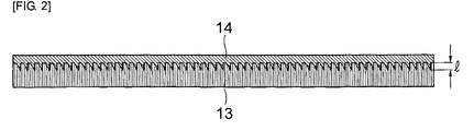
- FIG. 2 is a cross-sectional view showing an example where a dummy sheet is bonded on a resist layer in accordance with an embodiment of the present invention.
- FIGS. 1A to 1F are views showing processes of forming post bumps in accordance with an embodiment of the present invention, respectively.
- a seed layer 12 for metal plating is formed on a substrate 11 , and a resist layer 13 having openings A provided as positions where the seed layer 12 is subjected to metal plating is formed.
- a dummy sheet 14 for exposing the openings A is formed on the resist layer 13 , and the openings A are subjected to metal plating to thereby form the post 15 , and after solder balls 16 are formed on the post 15 , the dummy sheet and the resist layer are removed.
- the seed layer 12 may be formed on the substrate 11 through deposition of conductive materials for metal plating.
- the substrate refers to a plat-like base material, and may be formed of at least one of an electronic device, a circuit substrate, and a semiconductor wafer.
- the seed layer 12 may play a role of an electrode during a subsequent process, i.e., electro plating.
- a photosensitive film layer is layered on the seed layer 12 , the photosensitive film layer is selectively exposed and developed so that regions corresponding to metal plating positions can be opened, and then a partial region is removed to thereby form the openings A. Therefore, in such a manner, it is possible to form the resist layer 13 having the openings A provided as positions where the seed layer 120 is subjected to metal plating.
- the resist layer 13 having the openings A formed therein may be formed in various manners except for the above-described method.
- a dry film having heat-resistance or liquid photosensitivity materials for exposing the photoresist by Ultra Violet (UV) rays may be used as the photosensitive film layer.
- the dry film comes to be closely adhered on the seed layer 12 by using a laminator, and liquid photosensitivity materials are coated and dried on the seed layer 12 to thereby form the photosensitive film layer.
- UV Ultra Violet
- the photosensitive film layer When UV rays are irradiated on the photosensitive film layer, the photosensitive film layer remaining except for light blocked regions is exposed. In this case, the exposed regions are cured by polymerization reaction, while the light blocked regions are unchanged.
- the dummy sheet 14 with the convex/concave is layered on the resist layer 13 , the dummy sheet 14 is forcedly adhered and bonded on the resist layer 13 .
- the bonding surface between the dummy sheet 14 and the resist layer 13 may be formed to have a metal thin film with the convex/concave structure. It is desirable that the width (I) of the convex/concave is formed to have a size of 10 micrometer or lower, for bonding in force (refer to FIG. 2 ).
- a bottom surface of the openings A is filled with a metallic material to thereby form the post 15 .
- solder balls 16 are formed on the post 15 .
- solder balls 16 on the post 15 In a method for forming the solder balls 16 on the post 15 , a solder paste is coated on the post 15 , and then the solder paste is subjected to squeezing and is forcedly inserted into a part of the remaining openings A.
- a solder ball may be formed in a dome shape where space partitioned by virtual lines extending toward an axis direction from an outer circumference of the post 15 is filled.
- a metal or a solder ball may be formed by at least one of a Sn—Pb based solder, a Sn—Ag based solder, and a Sn—Ag—Cu based solder.
- the dummy sheet 14 is removed by using a vacuum pad, and the photosensitive film layer remaining on the seed layer 12 is removed.
- the resist layer 13 having the openings A formed therein is formed, and then copper plating is performed without layering the dummy sheet.
- a shape of the post 15 formed on Cu-excessive-plating region is different from a shape of the post 15 formed on Cu-uniform-plating region.
- Cu-excessive-plating means that Cu is excessively plated and the term Cu-uniform-plating means that Cu is uniformly plated compared with the Cu-excessive-plating region.
- the seed layer 12 serves as an anode and a part for providing copper Cu serves as a cathode in a process of performing copper plating of the openings A.
- one surface of the dummy sheet adjacent to the resist layer is formed to be in a convex/concave shape, and is forcedly bonded on the resist layer, so that it is possible to separate the dummy sheet through a vacuum pad after formation of the post bumps, and to delaminate and dry copper used for plating in etching lines of the separated dummy sheet to thereby provide reuse effect.
Abstract
Description
Claims (19)
Applications Claiming Priority (2)
| Application Number | Priority Date | Filing Date | Title |
|---|---|---|---|
| KR10-2009-0107530 | 2009-11-09 | ||
| KR1020090107530A KR101023296B1 (en) | 2009-11-09 | 2009-11-09 | Forming method of post bump |
Publications (2)
| Publication Number | Publication Date |
|---|---|
| US20110111587A1 US20110111587A1 (en) | 2011-05-12 |
| US8084349B2 true US8084349B2 (en) | 2011-12-27 |
Family
ID=43939136
Family Applications (1)
| Application Number | Title | Priority Date | Filing Date |
|---|---|---|---|
| US12/752,896 Expired - Fee Related US8084349B2 (en) | 2009-11-09 | 2010-04-01 | Method for forming post bump |
Country Status (2)
| Country | Link |
|---|---|
| US (1) | US8084349B2 (en) |
| KR (1) | KR101023296B1 (en) |
Families Citing this family (2)
| Publication number | Priority date | Publication date | Assignee | Title |
|---|---|---|---|---|
| WO2013088982A1 (en) * | 2011-12-12 | 2013-06-20 | ソニー株式会社 | Client terminal, client terminal operating method, transmission server, transmission server operating method, and program |
| KR101631405B1 (en) * | 2015-01-29 | 2016-06-17 | 앰코 테크놀로지 코리아 주식회사 | Method for fabricating semiconductor package and semiconductor package using the same |
Citations (12)
| Publication number | Priority date | Publication date | Assignee | Title |
|---|---|---|---|---|
| JPH05166815A (en) | 1991-12-16 | 1993-07-02 | Matsushita Electron Corp | Plating bump formation method and wafer plating jigs adopted |
| US5411918A (en) * | 1990-07-18 | 1995-05-02 | Raychem Limited | Processing microchips |
| US6547124B2 (en) * | 2001-06-14 | 2003-04-15 | Bae Systems Information And Electronic Systems Integration Inc. | Method for forming a micro column grid array (CGA) |
| US6630742B2 (en) * | 1999-12-27 | 2003-10-07 | Fujitsu Limited | Method for forming bumps, semiconductor device, and solder paste |
| US6706554B2 (en) * | 2000-10-26 | 2004-03-16 | Oki Electric Industry Co., Ltd. | Conductor posts, construction for and method of fabricating semiconductor integrated circuit chips using the conductor post, and method of probing semiconductor integrated circuit chips |
| US6723630B2 (en) * | 2002-02-27 | 2004-04-20 | Advanced Semiconductor Engineering, Inc. | Solder ball fabrication process |
| US20040082161A1 (en) * | 2002-10-25 | 2004-04-29 | Kwun-Yao Ho | Process of forming bonding columns |
| US6784087B2 (en) * | 2002-01-07 | 2004-08-31 | Megic Corporation | Method of fabricating cylindrical bonding structure |
| US6861346B2 (en) * | 2002-02-27 | 2005-03-01 | Advanced Semiconductor Engineering, Inc. | Solder ball fabricating process |
| US20060087034A1 (en) * | 2004-10-22 | 2006-04-27 | Advanced Semiconductor Engineering, Inc. | Bumping process and structure thereof |
| US7670874B2 (en) * | 2007-02-16 | 2010-03-02 | John Trezza | Plated pillar package formation |
| US7892962B2 (en) * | 2007-09-05 | 2011-02-22 | Taiwan Semiconductor Manufacturing Company, Ltd. | Nail-shaped pillar for wafer-level chip-scale packaging |
Family Cites Families (4)
| Publication number | Priority date | Publication date | Assignee | Title |
|---|---|---|---|---|
| JPH08222840A (en) * | 1995-02-15 | 1996-08-30 | Sumitomo Metal Ind Ltd | Circuit board with electrode pad and its manufacture |
| JP4514308B2 (en) | 2000-10-19 | 2010-07-28 | イビデン株式会社 | Manufacturing method of multilayer printed wiring board |
| JP4748889B2 (en) | 2000-12-26 | 2011-08-17 | イビデン株式会社 | Manufacturing method of multilayer printed wiring board |
| KR100712033B1 (en) | 2006-03-09 | 2007-05-02 | 와이엠티 주식회사 | Palladium-gold plating process to solve a large thickness distribution on high density printed circuit board and printed circuit board produced therefrom |
-
2009
- 2009-11-09 KR KR1020090107530A patent/KR101023296B1/en not_active IP Right Cessation
-
2010
- 2010-04-01 US US12/752,896 patent/US8084349B2/en not_active Expired - Fee Related
Patent Citations (12)
| Publication number | Priority date | Publication date | Assignee | Title |
|---|---|---|---|---|
| US5411918A (en) * | 1990-07-18 | 1995-05-02 | Raychem Limited | Processing microchips |
| JPH05166815A (en) | 1991-12-16 | 1993-07-02 | Matsushita Electron Corp | Plating bump formation method and wafer plating jigs adopted |
| US6630742B2 (en) * | 1999-12-27 | 2003-10-07 | Fujitsu Limited | Method for forming bumps, semiconductor device, and solder paste |
| US6706554B2 (en) * | 2000-10-26 | 2004-03-16 | Oki Electric Industry Co., Ltd. | Conductor posts, construction for and method of fabricating semiconductor integrated circuit chips using the conductor post, and method of probing semiconductor integrated circuit chips |
| US6547124B2 (en) * | 2001-06-14 | 2003-04-15 | Bae Systems Information And Electronic Systems Integration Inc. | Method for forming a micro column grid array (CGA) |
| US6784087B2 (en) * | 2002-01-07 | 2004-08-31 | Megic Corporation | Method of fabricating cylindrical bonding structure |
| US6723630B2 (en) * | 2002-02-27 | 2004-04-20 | Advanced Semiconductor Engineering, Inc. | Solder ball fabrication process |
| US6861346B2 (en) * | 2002-02-27 | 2005-03-01 | Advanced Semiconductor Engineering, Inc. | Solder ball fabricating process |
| US20040082161A1 (en) * | 2002-10-25 | 2004-04-29 | Kwun-Yao Ho | Process of forming bonding columns |
| US20060087034A1 (en) * | 2004-10-22 | 2006-04-27 | Advanced Semiconductor Engineering, Inc. | Bumping process and structure thereof |
| US7670874B2 (en) * | 2007-02-16 | 2010-03-02 | John Trezza | Plated pillar package formation |
| US7892962B2 (en) * | 2007-09-05 | 2011-02-22 | Taiwan Semiconductor Manufacturing Company, Ltd. | Nail-shaped pillar for wafer-level chip-scale packaging |
Also Published As
| Publication number | Publication date |
|---|---|
| US20110111587A1 (en) | 2011-05-12 |
| KR101023296B1 (en) | 2011-03-18 |
Similar Documents
| Publication | Publication Date | Title |
|---|---|---|
| US7705471B2 (en) | Conductive bump structure of circuit board and method for forming the same | |
| US6041495A (en) | Method of manufacturing a circuit board having metal bumps and a semiconductor device package comprising the same | |
| US7632709B2 (en) | Method of manufacturing wafer level package | |
| US7875805B2 (en) | Warpage-proof circuit board structure | |
| US7670962B2 (en) | Substrate having stiffener fabrication method | |
| US6872590B2 (en) | Package substrate for electrolytic leadless plating and manufacturing method thereof | |
| US7151050B2 (en) | Method for fabricating electrical connection structure of circuit board | |
| US20080258293A1 (en) | Semiconductor device package to improve functions of heat sink and ground shield | |
| KR101609016B1 (en) | Semiconductor device and method of manufacturing substrates for semiconductor elements | |
| US20060134826A1 (en) | Methods of forming semiconductor packages | |
| US20120138337A1 (en) | Printed circuit board and method of manufacturing the same | |
| US20080185711A1 (en) | Semiconductor package substrate | |
| US9324580B2 (en) | Process for fabricating a circuit substrate | |
| US7521800B2 (en) | Solder pad and method of making the same | |
| US20090102050A1 (en) | Solder ball disposing surface structure of package substrate | |
| US20110299259A1 (en) | Circuit board with conductor post structure | |
| US20070290344A1 (en) | Printed circuit board for package of electronic components and manufacturing method thereof | |
| JP2007088477A (en) | Method for manufacturing substrate provided with cavity | |
| TWI419630B (en) | Embedded printed circuit board and method of manufacturing the same | |
| US20210296260A1 (en) | Semiconductor packaging substrate, fabrication method and packaging process thereof | |
| US8084349B2 (en) | Method for forming post bump | |
| CN109686669B (en) | Integrated circuit packaging method and packaging structure | |
| TWI669034B (en) | Printed circuit board structure and method of forming the same | |
| US7544599B2 (en) | Manufacturing method of solder ball disposing surface structure of package substrate | |
| US20090124043A1 (en) | Method of manufacturing a package board |
Legal Events
| Date | Code | Title | Description |
|---|---|---|---|
| AS | Assignment |
Owner name: SAMSUNG ELECTRO-MECHANICS CO., LTD., KOREA, REPUBL Free format text: ASSIGNMENT OF ASSIGNORS INTEREST;ASSIGNOR:HONG, DAE JO;REEL/FRAME:024177/0106 Effective date: 20091109 |
|
| FEPP | Fee payment procedure |
Free format text: PAYOR NUMBER ASSIGNED (ORIGINAL EVENT CODE: ASPN); ENTITY STATUS OF PATENT OWNER: LARGE ENTITY |
|
| STCF | Information on status: patent grant |
Free format text: PATENTED CASE |
|
| FPAY | Fee payment |
Year of fee payment: 4 |
|
| FEPP | Fee payment procedure |
Free format text: MAINTENANCE FEE REMINDER MAILED (ORIGINAL EVENT CODE: REM.); ENTITY STATUS OF PATENT OWNER: LARGE ENTITY |
|
| LAPS | Lapse for failure to pay maintenance fees |
Free format text: PATENT EXPIRED FOR FAILURE TO PAY MAINTENANCE FEES (ORIGINAL EVENT CODE: EXP.); ENTITY STATUS OF PATENT OWNER: LARGE ENTITY |
|
| STCH | Information on status: patent discontinuation |
Free format text: PATENT EXPIRED DUE TO NONPAYMENT OF MAINTENANCE FEES UNDER 37 CFR 1.362 |
|
| FP | Lapsed due to failure to pay maintenance fee |
Effective date: 20191227 |