US8083309B2 - Liquid ejecting apparatus and liquid ejecting method - Google Patents

Liquid ejecting apparatus and liquid ejecting method Download PDF

Info

Publication number
US8083309B2
US8083309B2 US12/145,725 US14572508A US8083309B2 US 8083309 B2 US8083309 B2 US 8083309B2 US 14572508 A US14572508 A US 14572508A US 8083309 B2 US8083309 B2 US 8083309B2
Authority
US
United States
Prior art keywords
voltage
current source
charge
current
charge emission
Prior art date
Legal status (The legal status is an assumption and is not a legal conclusion. Google has not performed a legal analysis and makes no representation as to the accuracy of the status listed.)
Active, expires
Application number
US12/145,725
Other versions
US20090002036A1 (en
Inventor
Atsushi Umeda
Current Assignee (The listed assignees may be inaccurate. Google has not performed a legal analysis and makes no representation or warranty as to the accuracy of the list.)
Seiko Epson Corp
Original Assignee
Seiko Epson Corp
Priority date (The priority date is an assumption and is not a legal conclusion. Google has not performed a legal analysis and makes no representation as to the accuracy of the date listed.)
Filing date
Publication date
Application filed by Seiko Epson Corp filed Critical Seiko Epson Corp
Assigned to SEIKO EPSON CORPORATION reassignment SEIKO EPSON CORPORATION ASSIGNMENT OF ASSIGNORS INTEREST (SEE DOCUMENT FOR DETAILS). Assignors: UMEDA, ATSUSHI
Publication of US20090002036A1 publication Critical patent/US20090002036A1/en
Application granted granted Critical
Publication of US8083309B2 publication Critical patent/US8083309B2/en
Active legal-status Critical Current
Adjusted expiration legal-status Critical

Links

Images

Classifications

    • HELECTRICITY
    • H03ELECTRONIC CIRCUITRY
    • H03KPULSE TECHNIQUE
    • H03K19/00Logic circuits, i.e. having at least two inputs acting on one output; Inverting circuits
    • H03K19/0175Coupling arrangements; Interface arrangements
    • H03K19/017509Interface arrangements
    • H03K19/017518Interface arrangements using a combination of bipolar and field effect transistors [BIFET]
    • BPERFORMING OPERATIONS; TRANSPORTING
    • B41PRINTING; LINING MACHINES; TYPEWRITERS; STAMPS
    • B41JTYPEWRITERS; SELECTIVE PRINTING MECHANISMS, i.e. MECHANISMS PRINTING OTHERWISE THAN FROM A FORME; CORRECTION OF TYPOGRAPHICAL ERRORS
    • B41J2/00Typewriters or selective printing mechanisms characterised by the printing or marking process for which they are designed
    • B41J2/005Typewriters or selective printing mechanisms characterised by the printing or marking process for which they are designed characterised by bringing liquid or particles selectively into contact with a printing material
    • B41J2/01Ink jet
    • B41J2/015Ink jet characterised by the jet generation process
    • B41J2/04Ink jet characterised by the jet generation process generating single droplets or particles on demand
    • B41J2/045Ink jet characterised by the jet generation process generating single droplets or particles on demand by pressure, e.g. electromechanical transducers
    • B41J2/04501Control methods or devices therefor, e.g. driver circuits, control circuits
    • B41J2/04541Specific driving circuit
    • BPERFORMING OPERATIONS; TRANSPORTING
    • B41PRINTING; LINING MACHINES; TYPEWRITERS; STAMPS
    • B41JTYPEWRITERS; SELECTIVE PRINTING MECHANISMS, i.e. MECHANISMS PRINTING OTHERWISE THAN FROM A FORME; CORRECTION OF TYPOGRAPHICAL ERRORS
    • B41J2/00Typewriters or selective printing mechanisms characterised by the printing or marking process for which they are designed
    • B41J2/005Typewriters or selective printing mechanisms characterised by the printing or marking process for which they are designed characterised by bringing liquid or particles selectively into contact with a printing material
    • B41J2/01Ink jet
    • B41J2/015Ink jet characterised by the jet generation process
    • B41J2/04Ink jet characterised by the jet generation process generating single droplets or particles on demand
    • B41J2/045Ink jet characterised by the jet generation process generating single droplets or particles on demand by pressure, e.g. electromechanical transducers
    • B41J2/04501Control methods or devices therefor, e.g. driver circuits, control circuits
    • B41J2/0455Details of switching sections of circuit, e.g. transistors
    • BPERFORMING OPERATIONS; TRANSPORTING
    • B41PRINTING; LINING MACHINES; TYPEWRITERS; STAMPS
    • B41JTYPEWRITERS; SELECTIVE PRINTING MECHANISMS, i.e. MECHANISMS PRINTING OTHERWISE THAN FROM A FORME; CORRECTION OF TYPOGRAPHICAL ERRORS
    • B41J2/00Typewriters or selective printing mechanisms characterised by the printing or marking process for which they are designed
    • B41J2/005Typewriters or selective printing mechanisms characterised by the printing or marking process for which they are designed characterised by bringing liquid or particles selectively into contact with a printing material
    • B41J2/01Ink jet
    • B41J2/015Ink jet characterised by the jet generation process
    • B41J2/04Ink jet characterised by the jet generation process generating single droplets or particles on demand
    • B41J2/045Ink jet characterised by the jet generation process generating single droplets or particles on demand by pressure, e.g. electromechanical transducers
    • B41J2/04501Control methods or devices therefor, e.g. driver circuits, control circuits
    • B41J2/04581Control methods or devices therefor, e.g. driver circuits, control circuits controlling heads based on piezoelectric elements
    • BPERFORMING OPERATIONS; TRANSPORTING
    • B41PRINTING; LINING MACHINES; TYPEWRITERS; STAMPS
    • B41JTYPEWRITERS; SELECTIVE PRINTING MECHANISMS, i.e. MECHANISMS PRINTING OTHERWISE THAN FROM A FORME; CORRECTION OF TYPOGRAPHICAL ERRORS
    • B41J2/00Typewriters or selective printing mechanisms characterised by the printing or marking process for which they are designed
    • B41J2/005Typewriters or selective printing mechanisms characterised by the printing or marking process for which they are designed characterised by bringing liquid or particles selectively into contact with a printing material
    • B41J2/01Ink jet
    • B41J2/015Ink jet characterised by the jet generation process
    • B41J2/04Ink jet characterised by the jet generation process generating single droplets or particles on demand
    • B41J2/045Ink jet characterised by the jet generation process generating single droplets or particles on demand by pressure, e.g. electromechanical transducers
    • B41J2/04501Control methods or devices therefor, e.g. driver circuits, control circuits
    • B41J2/04588Control methods or devices therefor, e.g. driver circuits, control circuits using a specific waveform
    • HELECTRICITY
    • H03ELECTRONIC CIRCUITRY
    • H03KPULSE TECHNIQUE
    • H03K17/00Electronic switching or gating, i.e. not by contact-making and –breaking
    • H03K17/51Electronic switching or gating, i.e. not by contact-making and –breaking characterised by the components used
    • H03K17/56Electronic switching or gating, i.e. not by contact-making and –breaking characterised by the components used by the use, as active elements, of semiconductor devices
    • H03K17/60Electronic switching or gating, i.e. not by contact-making and –breaking characterised by the components used by the use, as active elements, of semiconductor devices the devices being bipolar transistors
    • H03K17/66Switching arrangements for passing the current in either direction at will; Switching arrangements for reversing the current at will
    • H03K17/665Switching arrangements for passing the current in either direction at will; Switching arrangements for reversing the current at will connected to one load terminal only
    • H03K17/666Switching arrangements for passing the current in either direction at will; Switching arrangements for reversing the current at will connected to one load terminal only the output circuit comprising more than one controlled bipolar transistor
    • H03K17/667Switching arrangements for passing the current in either direction at will; Switching arrangements for reversing the current at will connected to one load terminal only the output circuit comprising more than one controlled bipolar transistor using complementary bipolar transistors
    • HELECTRICITY
    • H03ELECTRONIC CIRCUITRY
    • H03KPULSE TECHNIQUE
    • H03K19/00Logic circuits, i.e. having at least two inputs acting on one output; Inverting circuits
    • H03K19/0008Arrangements for reducing power consumption
    • HELECTRICITY
    • H03ELECTRONIC CIRCUITRY
    • H03KPULSE TECHNIQUE
    • H03K19/00Logic circuits, i.e. having at least two inputs acting on one output; Inverting circuits
    • H03K19/01Modifications for accelerating switching
    • H03K19/013Modifications for accelerating switching in bipolar transistor circuits
    • H03K19/0136Modifications for accelerating switching in bipolar transistor circuits by means of a pull-up or down element
    • HELECTRICITY
    • H03ELECTRONIC CIRCUITRY
    • H03KPULSE TECHNIQUE
    • H03K2217/00Indexing scheme related to electronic switching or gating, i.e. not by contact-making or -breaking covered by H03K17/00
    • H03K2217/0036Means reducing energy consumption

Definitions

  • the present invention relates to a liquid ejecting apparatus and a liquid ejecting method.
  • Known liquid ejecting apparatuses include an element which is charged and discharged so as to perform an operation to eject a liquid, and a transistor which pushes a current to the element or pulls a current from the element.
  • Such liquid ejecting apparatuses generate a driving signal by amplifying the current of an analog signal input to a bipolar transistor and apply the driving signal to the element.
  • One such liquid ejecting apparatus is provided with two pairs of transistors, to which different power supply voltages are applied, in order to suppress power consumption in the transistor (for example, see JP-A-11-170529).
  • the pairs of transistors are switched according to the voltage of the analog signal. Accordingly, power saving can be achieved, compared with a case in which a pair of transistors are provided.
  • the sets of transistors amplify the current.
  • An advantage of some aspects of the invention is that it is possible to achieve power saving.
  • a liquid ejection apparatus includes an element that is charged and discharged so as to perform an operation to eject a liquid, an analog signal generating unit that generates an analog signal having a voltage change pattern for determining the operation of the element, a charging transistor that amplifies a current of the analog signal while the element is charged, and pushes the amplified current toward the element, the charging transistor having a current source terminal, to which a current source is connected, and a push terminal for pushing the current, and a current source connector that selects at least one of a plurality of current sources according to a voltage of the analog signal, and connects the selected current source to the current source terminal.
  • FIG. 1 is a block diagram illustrating the configuration of a printing system.
  • FIG. 2 is a diagram illustrating a driving signal generating circuit and a peripheral portion according to a first embodiment of the invention.
  • FIG. 3 is a diagram illustrating a voltage waveform signal and a driving signal according to the first embodiment.
  • FIG. 4 is a diagram schematically illustrating a state where a capacitor is selected as a current source.
  • FIG. 5 is a diagram schematically illustrating a state where a first power generating circuit is selected as a current source.
  • FIG. 6 is a diagram schematically illustrating a state where a capacitor is selected as a charge emission destination.
  • FIG. 7 is a diagram schematically illustrating a state where a ground is selected as a charge emission destination.
  • FIG. 8 is a diagram illustrating a driving signal generating circuit and a peripheral portion according to a second embodiment of the invention.
  • FIG. 9 is a diagram illustrating a voltage waveform signal and a driving signal according to the second embodiment.
  • a liquid ejecting apparatus includes an element that is charged and discharged so as to perform an operation to eject a liquid, an analog signal generating unit that generates an analog signal having a voltage change pattern for determining the operation of the element, a charging transistor that amplifies a current of the analog while the element is charged, and pushes the amplified current toward the element, the charging transistor having a current source terminal, to which a current source is connected, and a push terminal for pushing the current, and a current source connector that selects at least one current source from among a plurality of current sources according to a voltage of the analog signal, and connects the selected current source to the current source terminal.
  • the current source connector may select at least one current source from among the plurality of current sources at different voltages.
  • the current source connector may switch a current source to be selected while the element is charged.
  • a current source suitable for the voltage of the analog signal can be used, thereby suppressing power consumption of the charging transistor.
  • the plurality of current sources may have a first current source at a first voltage and a second current source at a second voltage lower than the first voltage.
  • the current source connector may include a current source switch that is provided between the first current source and the current source terminal, and a control circuit that outputs, to the current source switch, a control signal at a voltage level determined to control the operation of the current source switch on the basis of the voltage of the analog signal.
  • the control circuit can determine a switching timing of the current source depending on setting, thereby preventing the analog signal from being distorted after being amplified.
  • the plurality of current sources may have a first current source at a first voltage and a second current source at a second voltage lower than the first voltage.
  • the current source connector may include a current source switch that is provided between the first current source and the current source terminal, and an element that is provided between the second current source and the current source terminal, and allows charge movement from the second current source to the current source terminal while blocking charge movement from the current source terminal to the second current source.
  • the current source switch may have a transistor.
  • connection or disconnection of the first current source can be controlled with simple configuration.
  • the first current source may have a power supply circuit
  • the second current source may have a capacitor
  • the capacitor may be charged with a charge to be moved while the element is discharged.
  • the liquid ejecting apparatus may further include a discharging transistor that amplifies the current of the analog signal while the element is discharged, and pulls the current from the element, the discharging transistor having a pull terminal for pulling the current and an emission terminal for emitting the charge, and a charge emission destination connector that selects at least one charge emission destination from among a plurality of charge emission destinations including the capacitor according to the voltage of the analog signal, and connects the selected charge emission destination to the emission terminal.
  • the second current source may emit the charge accumulated in the capacitor while the element is charged.
  • a liquid ejecting apparatus includes an element that is charged and discharged so as to perform an operation to eject a liquid, an analog signal generating unit that generates an analog signal having a voltage change pattern for determining the operation of the element, a discharging transistor that amplifies the current of the analog signal while the element is discharged, and pulls the current from the element, the discharging transistor having a pull terminal for pulling the current and an emission terminal for emitting the charge, and a charge emission destination connector that selects at least one charge emission destination from among a plurality of charge emission destinations according to the voltage of the analog signal, and connects the selected charge emission destination to the emission terminal.
  • the charge emission destination connector may select at least one charge emission destination from among a plurality of charge emission destinations at different voltages.
  • the charge emission destination connector may switch a charge emission destination to be selected while the element is discharged.
  • the charge can be emitted to a charge emission destination suitable for the voltage of the analog signal, thereby suppressing power consumption of the discharging transistor.
  • the plurality of charge emission destinations may have a first charge emission destination at a first voltage, and a second charge emission destination at a second voltage higher than the first voltage.
  • the charge emission destination connector may have a charge emission destination switch that is provided between the emission terminal and the first charge emission destination, and a control circuit that outputs, to the charge emission destination switch, a control signal at a voltage level determined to control the operation of the charge emission destination switch on the basis of the voltage of the analog signal.
  • the control circuit can determine a switching timing of the charge emission destination depending on setting, thereby preventing the analog signal from being distorted after being amplified.
  • the plurality of charge emission destinations may have a first charge emission destination at a first voltage, and a second charge emission destination at a second voltage higher than the first voltage.
  • the charge emission destination connector may include a charge emission destination switch that is provided between the emission terminal and the first charge emission destination, and an element that is provided between the emission terminal and the second charge emission destination, and allows charge movement from the emission terminal to the second charge emission destination, while blocking charge movement from the second charge emission destination to the emission terminal.
  • the charge emission destination switch may be a transistor.
  • connection or disconnection of the first charge emission destination can be controlled with simple configuration.
  • the first charge emission destination may be a ground
  • the second charge emission destination may be a capacitor
  • a liquid ejecting method includes generating an analog signal having a voltage change pattern for determining an operation of an element, which is charged and discharged so as to perform an operation to eject a liquid, while the element is charged, selecting at least one current source from among a plurality of current sources according to a voltage of the analog signal, and amplifying a current of the analog signal by the selected current source and pushing the amplified current toward the element.
  • a liquid ejecting method includes generating an analog signal having a voltage change pattern for determining an operation of an element, which is charged and discharged so as to perform an operation to eject a liquid, while the element is discharged, selecting at least one charge emission destination from among a plurality of charge emission destinations according to a voltage of the analog signal, and amplifying a current of the analog signal, pulling a current from the element, and emitting a charge to the selected charge emission destination.
  • FIG. 1 is a block diagram illustrating the configuration of a printing system.
  • a printing system shown in FIG. 1 has a printer 1 and a computer CP.
  • the printer 1 corresponds to a liquid ejecting apparatus, and ejects ink (a kind of liquid) onto a medium, such as paper, cloth, or film. It should be noted that the medium corresponds to a target on which the liquid is to be ejected.
  • the computer CP is communicably connected to the printer 1 .
  • the computer CP transmits print data corresponding to the image to the printer 1 .
  • the print data includes dot forming data.
  • the dot forming data is data regarding a dot to be formed on the paper (data regarding color and size of the dot).
  • the dot forming data is, for example, two-bit data.
  • the printer 1 has a paper transport mechanism 20 , a carriage moving mechanism 30 , a driving signal generating circuit 40 , a head unit 50 , a detector group 60 , a printer-side controller 70 , and a power supply 80 .
  • the paper transport mechanism 20 transports a paper serving as a medium in a transport direction.
  • the carriage moving mechanism 30 moves the head unit 50 in a predetermined direction (for example, a paper widthwise direction).
  • a head 52 in the head unit 50 ejects ink (a kind of liquid) onto the paper.
  • the driving signal generating circuit 40 generates a driving signal COM.
  • the driving signal COM is used during printing on the paper.
  • the driving signal COM is a series of signals including a driving pulse.
  • the driving pulse is a voltage change pattern that causes a piezoelectric element 52 a (see FIG. 2 ) in the head 52 to perform a predetermined operation.
  • the head unit 50 has a head control section 51 and a head 52 .
  • the head 52 has a piezoelectric element 52 a .
  • the piezoelectric element 52 a corresponds to an element that performs an operation to eject the liquid.
  • a plurality of piezoelectric elements 52 a are provided to correspond to nozzles (not shown) in the head 52 .
  • 96 to 180 piezoelectric elements 52 a are provided for each color.
  • Each of the piezoelectric elements 52 a is a kind of a capacitive element capable holding a charge, and is charged or discharged by applying a required segment of the driving signal COM.
  • the piezoelectric element 52 a is deformed according to charging/discharging, such that ink stored in a pressure chamber (not shown) of the head 52 undergoes a change in pressure. Due to the change in pressure, ink is ejected from the nozzles. Accordingly, the deformation of the piezoelectric element 52 a corresponds to the operation to eject ink. This operation is determined by the voltage change pattern of the driving signal COM.
  • the head control section 51 selectively applies, to the piezoelectric elements 52 a , the required segment of the driving signal COM generated by the driving signal generating circuit 40 .
  • the head control section 51 has a plurality of switches 51 a that are provided to correspond to the piezoelectric elements 52 a in a supply line of the driving signal COM. Then, the head control section 51 controls the switches 51 a to apply the required segment of the driving signal COM to the piezoelectric elements 52 a .
  • a desired amount of ink can be ejected from the nozzles if the required segment is appropriately selected.
  • the detector group 60 has a plurality of detectors for monitoring the states of the printer 1 .
  • the detection results by the detectors are output to the printer-side controller 70 .
  • the printer-side controller 70 controls the individual units on the basis of the print data from the computer CP and the detection results from the detectors to print an image on the paper.
  • the power supply 80 generates power to be supplied to a current amplifying transistor in the driving signal generating circuit 40 .
  • the power supply 80 has a first power generating circuit 81 which generates a first power supply voltage (42 V), and a second power generating circuit 82 which generates a second power supply voltage (24 V).
  • the first power generating circuit 81 corresponds to a power supply circuit.
  • the printer-side controller 70 performs the overall control of the printer 1 .
  • the printer-side controller 70 controls the paper transport mechanism 20 , the carriage moving mechanism 30 , the driving signal generating circuit 40 , and the head unit 50 .
  • the printer-side controller 70 has an interface section 71 , a CPU (Central Processing Unit) 72 , a memory 73 , and a control unit 74 .
  • the interface section 71 exchanges data with the computer CP.
  • the CPU 72 performs the overall control of the printer 1 .
  • the memory 73 reserves an area for storing computer programs and a working area.
  • the CPU 72 controls the individual units according to the computer programs stored in the memory 73 .
  • the CPU 72 controls the paper transport mechanism 20 or the carriage moving mechanism 30 by means of the control unit 74 .
  • the CPU 72 transmits a head control signal for controlling the operation of the head 52 to the head control section 51 or transmits a control signal for generating the driving signal COM to the driving signal generating circuit 40 .
  • the control signal for generating the driving signal COM is also referred to as DAC data which is, for example, multi-bit digital data.
  • the DAC data is data for determining the voltage change pattern of the driving signal COM generated by the driving signal generating circuit 40 . That is, the DAC data determines a voltage of a voltage waveform signal COM′ which is generated by a waveform generating circuit 41 (see FIG. 2 ) in the driving signal generating circuit 40 .
  • the DAC data may be said to indirectly indicate the voltage of the driving signal COM, and thus it corresponds to voltage waveform information.
  • the DAC data is stored in a predetermined area of the memory 73 . Then, the DAC data is read out by the CPU 72 when the driving signal COM is generated.
  • the driving signal generating circuit 40 corresponds to a driving signal generating device which generates the driving signal COM. Accordingly, the printer 1 may be said to be a liquid ejecting apparatus having incorporated therein a driving signal generating device. As shown in FIG. 2 , the driving signal generating circuit 40 has a waveform generating circuit 41 , a current amplifying circuit 42 , a capacitor 43 , a first selection circuit 44 , and a second selection circuit 45 .
  • the waveform generating circuit 41 generates a voltage waveform signal COM′ having a voltage change pattern determined by the DAC data. That is, the waveform generating circuit 41 has a digital-to-analog converter that converts the DAC data as digital data into the voltage waveform signal COM′ as an analog signal.
  • the voltage waveform signal COM′ is a signal having a basic voltage waveform of the driving signal COM. That is, the voltage waveform signal COM′ may be said to be a signal for determining the voltage change pattern of the driving signal COM.
  • the piezoelectric element 52 a operates according to the voltage change pattern of an applied segment of the driving signal COM.
  • the voltage waveform signal COM′ corresponds to an analog signal having a voltage change pattern for determining the operation of the piezoelectric element 52 a .
  • the waveform generating circuit 41 corresponds to an analog signal generator which generates an analog signal.
  • the waveform generating circuit 41 is provided with output terminals of the voltage waveform signal COM′ for two channels. This is because two transistors in the current amplifying circuit 42 use the voltage waveform signal COM′.
  • the current amplifying circuit 42 corresponds to a current amplifier.
  • the current amplifying circuit 42 amplifies a current of the voltage waveform signal COM′ as an analog signal, and outputs the amplified signal as the driving signal COM.
  • the current amplifying circuit 42 has an NPN transistor 42 a and a PNP transistor 42 b , which are connected with each other in a complementary manner, as current amplifying transistors.
  • the NPN transistor 42 a is a charging transistor which operates while the piezoelectric element 52 a is charged.
  • a collector of the NPN transistor 42 a is connected to the first power generating circuit 81 or the capacitor 43 through the first selection circuit 44 .
  • An emitter of the NPN transistor 42 a is connected to a supply line of the driving signal COM, and a base of the NPN transistor 42 a is connected to a supply line of the voltage waveform signal COM′.
  • the NPN transistor 42 a is turned on when the voltage of the voltage waveform signal COM′ increases, and amplifies a current of the voltage waveform signal COM′ and pushes the amplified current to the piezoelectric element 52 a .
  • the first power generating circuit 81 or the capacitor 43 functions as a current source. Accordingly, the collector of the NPN transistor 42 a corresponds to a current source terminal to which a current source is connected. In addition, the amplified current is pushed from the emitter of the NPN transistor 42 a . Accordingly, the emitter corresponds to a push terminal for pushing a current. Furthermore, the voltage waveform signal COM′ (analog signal) is input to the base of the NPN transistor 42 a . That is, the base of the NPN transistor 42 a corresponds to an analog signal input terminal to which an analog signal is input.
  • COM′ analog signal
  • the PNP transistor 42 b is a discharging transistor which operates when the piezoelectric element 52 a is discharged.
  • An emitter of the PNP transistor 42 b is connected to the supply line of the driving signal COM, and a base of the PNP transistor 42 b is connected to the supply line of the voltage waveform signal COM′.
  • a collector of the PNP transistor 42 b is connected to a ground or the capacitor 43 through the second selection circuit 45 .
  • the PNP transistor 42 b is turned on when the voltage of the voltage waveform signal COM′ decreases, and amplifies the current of the voltage waveform signal COM′ and pulls the current from the piezoelectric element 52 a . During the current amplification, the current is pulled from the emitter.
  • the emitter of the PNP transistor 42 b corresponds to a pull terminal for pulling a current.
  • a charge is emitted from the collector of the PNP transistor 42 b to the ground or the capacitor 43 through the second selection circuit 45 .
  • the collector of the PNP transistor 42 b corresponds to an emission terminal for emitting the charge.
  • the ground or the capacitor 43 corresponds to a charge emission destination.
  • the voltage waveform signal COM′ (analog signal) is input to the base of the PNP transistor 42 b . That is, the base of the PNP transistor 42 b corresponds to an analog signal input terminal to which an analog signal is input.
  • the operations of the transistors 42 a and 42 b are controlled by the voltage waveform signal COM′ output from the waveform generating circuit 41 .
  • the voltage of the driving signal COM output from the current amplifying circuit 42 is slightly changed during the current amplification, but it becomes almost equal to the voltage of the voltage waveform signal COM′.
  • the capacitor 43 functions as a current source with respect to the NPN transistor 42 a . Meanwhile, the capacitor 43 functions as a charge emission destination with respect to the PNP transistor 42 b .
  • the capacitor 43 has a regular voltage of 24 V, and a positive terminal thereof is connected to the second power generating circuit 82 through a resistor 82 a . Accordingly, the capacitor 43 is gradually charged with the second power supply voltage of 24 V, and functions as a 24 V current source.
  • the positive terminal of the capacitor 43 is connected to the collector of the NPN transistor 42 a through the first selection circuit 44 , and the collector of the PNP transistor 42 b through the second selection circuit 45 .
  • the first selection circuit 44 connects the capacitor 43 to the collector of the NPN transistor 42 a when the voltage of the voltage waveform signal COM′ is less than a predetermined voltage.
  • the first selection circuit 44 connects the first power generating circuit 81 to the collector of the NPN transistor 42 a .
  • the first power generating circuit 81 functions as a current source with respect to the NPN transistor 42 a , similarly to the capacitor 43 .
  • the first power supply voltage generated by the first power generating circuit 81 is 42 V.
  • a voltage to be supplied from the capacitor 43 is 24 V, which is lower than the first power supply voltage.
  • the first power generating circuit 81 corresponds to a first current source at a first voltage
  • the capacitor 43 corresponds to a second current source at a second voltage lower than the first voltage.
  • the second selection circuit 45 connects the ground to the collector of the PNP transistor 42 b when the voltage of the voltage waveform signal COM′ equal to or less than the predetermined voltage. When the voltage of the voltage waveform signal COM′ is more than the predetermined voltage, the second selection circuit 45 connects the capacitor 43 to the collector of the PNP transistor 42 b .
  • the ground and the capacitor 43 correspond to a charge emission destination with the PNP transistor 42 b .
  • the ground is at 0 V, and the voltage to be supplied from the capacitor 43 is 24 V. That is, the voltage to be supplied from the capacitor 43 is higher than the voltage of the ground. Accordingly, the ground corresponds to a first charge emission destination at a first voltage, and the capacitor 43 corresponds to a second charge emission destination at a second voltage higher than the first voltage.
  • the first selection circuit 44 selectively connects the first power generating circuit 81 and the capacitor 43 serving as the current source to the collector of the NPN transistor 42 a according to the voltage of the voltage waveform signal COM′. That is, the first selection circuit 44 corresponds to a current source connector that selects at least one current source from among a plurality of current sources according to the voltage of the analog signal, and connects the selected current source to the current source terminal.
  • the first selection circuit 44 has a first PNP transistor 44 a , a first NPN transistor 44 b , and a first diode 44 c.
  • the first PNP transistor 44 a functions as a current source switch, and controls connection or disconnection of the first power generating circuit 81 with respect to the collector of the NPN transistor 42 a in the current amplifying circuit 42 .
  • An emitter of the first PNP transistor 44 a is connected to the first power generating circuit 81 , and a collector of the first PNP transistor 44 a is connected to the collector of the NPN transistor 42 a .
  • a base of the first PNP transistor 44 a is connected to a collector of the first NPN transistor 44 b through a resistor 44 d.
  • the first NPN transistor 44 b functions as a control signal generating element, and generates a control signal for controlling the operation of the first PNP transistor 44 a on the basis of the voltage waveform signal COM′ (analog signal).
  • An emitter of the first NPN transistor 44 b is connected to the positive terminal of the capacitor 43 , and a base of the first NPN transistor 44 b is connected to the supply line of the voltage waveform signal COM′ through a resistor 44 e .
  • a collector of the first NPN transistor 44 b is connected to the base of the first PNP transistor 44 a through the resistor 44 d , as described above.
  • the first diode 44 c supplies a charge accumulated in the capacitor 43 to the collector of the NPN transistor 42 a when the first power generating circuit 81 is not connected to the NPN transistor 42 a in the current amplifying circuit 42 . That is, the first diode 44 c allows charge movement to the NPN transistor 42 a . Meanwhile, the first diode 44 c blocks the supply of the first power supply voltage to the capacitor 43 when the first power generating circuit 81 is connected to the collector of the NPN transistor 42 a .
  • a cathode of the first diode 44 c is connected to the collector of the NPN transistor 42 a in the current amplifying circuit 42 , and an anode of the first diode 44 c is connected to the positive terminal of the capacitor 43 .
  • the first diode 44 c is a kind of an element that blocks charge movement in a predetermined direction, and corresponds to a current source diode.
  • the emitter of the first NPN transistor 44 b is connected to the positive terminal of the capacitor 43 . Accordingly, when the voltage of the voltage waveform signal COM′ is less than a predetermined voltage (a voltage obtained by adding 0.6 V to the voltage to be supplied from the capacitor 43 ), the first NPN transistor 44 b is turned off. In this case, the potentials of the emitter and the base of the first PNP transistor 44 a are equalized, and thus the first PNP transistor 44 a is also turned off. As a result, the capacitor 43 serving as a second current source is connected to the NPN transistor 42 a in the current amplifying circuit 42 . That is, the NPN transistor 42 a in the current amplifying circuit 42 and the capacitor 43 are connected with each other through the first diode 44 c to allow charge movement.
  • a predetermined voltage a voltage obtained by adding 0.6 V to the voltage to be supplied from the capacitor 43
  • the first NPN transistor 44 b is turned on. In this case, the emitter and the collector of the first NPN transistor 44 b substantially have the same voltage. That is, the voltages of the emitter and the collector are equalized at the voltage to be supplied from the capacitor 43 . Accordingly, the voltage of the base of the first PNP transistor 44 a decreases to the voltage to be supplied from the capacitor 43 . Then, the first PNP transistor 44 a is turned on, and the emitter and the collector thereof substantially have the same voltage. That is, the voltages of the emitter and the collector are equalized at the first power supply voltage.
  • the first power generating circuit 81 serving as a first current source is connected to the NPN transistor 42 a in the current amplifying circuit 42 .
  • the voltage on the cathode of the first diode 44 c becomes sufficiently higher than the voltage on the anode of the first diode 44 c .
  • charge movement from the capacitor 43 to the NPN transistor 42 a is not performed. That is, the capacitor 43 and the NPN transistor 42 a are electrically disconnected from each other.
  • the second selection circuit 45 selectively connects the collector of the PNP transistor 42 b to the ground and the capacitor 43 serving as the charge emission destination according to the voltage of the voltage waveform signal COM′. Accordingly, the second selection circuit 45 corresponds to a charge emission destination connector that selects at least one charge emission destination from among a plurality of charge emission destinations according to a voltage of an analog signal, and connects the selected charge emission destination to an emission terminal.
  • the second selection circuit 45 includes a second NPN transistor 45 a , a second PNP transistor 45 b , and a second diode 45 c.
  • the second NPN transistor 45 a functions as a charge emission destination switch, and controls connection or disconnection from the ground with respect to the collector of the PNP transistor 42 b in the current amplifying circuit 42 .
  • a collector of the second NPN transistor 45 a is connected to the collector of the PNP transistor 42 b , and an emitter of the second NPN transistor 45 a is connected to the ground.
  • a base of the second NPN transistor 45 a is connected to a collector of the second PNP transistor 45 b through a resistor 45 d.
  • the second PNP transistor 45 b functions as a control signal generating element, and generates a control signal for controlling the operation of the second NPN transistor 45 a on the basis of the voltage waveform signal COM′ (analog signal).
  • An emitter of the second PNP transistor 45 b is connected to the positive terminal of the capacitor 43 , and a base of the second PNP transistor 45 b is connected to the supply line of the voltage waveform signal COM′ through a resistor 45 e .
  • a collector of the second PNP transistor 45 b is connected to the base of the second NPN transistor 45 a through the resistor 45 d , as described above.
  • the second diode 45 c moves a charge emitted from the collector of the PNP transistor 42 b to the capacitor 43 when the ground is not connected to the collector of the PNP transistor 42 b in the current amplifying circuit 42 . That is, the second diode 45 c allows charge movement to the capacitor 43 . Meanwhile, the second diode 45 c blocks emission of the charge accumulated in the capacitor 43 when the ground is connected to the collector of the PNP transistor 42 b . To this end, a cathode of the second diode 45 c is connected to the positive terminal of the capacitor 43 , and an anode of the second diode 45 c is connected to the collector of the PNP transistor 42 b .
  • the second diode 45 c is a kind of element that blocks charge movement in a predetermined direction, and corresponds to a discharging diode.
  • the emitter of the second PNP transistor 45 b is connected to the positive terminal of the capacitor 43 . Accordingly, when the voltage of the voltage waveform signal COM′ is higher than a predetermined voltage (a voltage obtained by subtracting 0.6 V from the voltage to be supplied from the capacitor 43 ), the second PNP transistor 45 b is turned off. In this case, the potentials of the emitter and the base of the second NPN transistor 45 a are equalized, and thus the second NPN transistor 45 a is also turned off. As a result, the capacitor 43 serving as a second charge emission destination is connected to the PNP transistor 42 b in the current amplifying circuit 42 . That is, the PNP transistor 42 b in the current amplifying circuit 42 and the capacitor 43 are connected with each other through the second diode 45 c to allow charge movement.
  • a predetermined voltage a voltage obtained by subtracting 0.6 V from the voltage to be supplied from the capacitor 43
  • the second PNP transistor 45 b is turned on. In this case, the emitter and the collector of the second PNP transistor 45 b substantially have the same voltage. That is, the voltages of the emitter and the collector are equalized at the voltage to be supplied from the capacitor 43 . Accordingly, the voltage of the base of the second NPN transistor 45 a increases to the voltage to be supplied from the capacitor 43 . Then, the second NPN transistor 45 a is turned on, and the emitter and the collector substantially have the same voltage. That is, the voltages of the emitter and the collector are equalized at the voltage of the ground.
  • the ground serving as a first charge emission destination is connected to the PNP transistor 42 b in the current amplifying circuit 42 .
  • the voltage on the cathode of the second diode 45 c becomes sufficiently higher than the voltage on the anode of the second diode 45 c .
  • no charge is moved from the capacitor 43 to the PNP transistor 42 b (ground). That is, the capacitor 43 and the PNP transistor 42 b are electrically disconnected from each other.
  • the printer 1 is characterized by the operation of the driving signal generating circuit 40 during printing.
  • the DAC data is output from the printer-side controller 70 to the waveform generating circuit 41 , and the voltage waveform signal COM′ (analog signal) having a voltage change pattern for determining the operation of the piezoelectric element 52 a is generated.
  • the first power generating circuit 81 and the capacitor 43 are selected according to the voltage of the voltage waveform signal COM′, and the current of the voltage waveform signal COM′ is amplified by means of the selected circuit and element. Then, the current is pushed toward the piezoelectric element 52 a .
  • the piezoelectric element 52 a while the piezoelectric element 52 a is discharged, the capacitor 43 and the ground are selected according to the voltage of the voltage waveform signal COM′. Then, the current of the voltage waveform signal COM′ is amplified, the current is pulled from the piezoelectric element 52 a , and the charge is emitted to the selected unit and element.
  • a heat sink can be compact. Furthermore, part of the charges emitted when the piezoelectric element 52 a is discharged is accumulated in the capacitor 43 serving as a second current source. Therefore, the charge can be effectively used, and thus power consumption can be suppressed.
  • the operation of the printer 1 will be described with particular emphasis on this point.
  • the printer-side controller 70 outputs DAC data at a voltage V 1 to the waveform generating circuit 41 . Accordingly, the waveform generating circuit 41 outputs a voltage waveform signal COM′ at a voltage V 1 during the corresponding period.
  • the voltage waveform signal COM′ is input to the base of the first NPN transistor 44 b in the first selection circuit 44 .
  • the voltage V 1 is sufficiently lower than the voltage (24 V) to be supplied from the capacitor 43 . For this reason, in the first selection circuit 44 , the first NPN transistor 44 b and the first PNP transistor 44 a are both turned off. Then, as indicated by a bold line in FIG.
  • the charge accumulated in the capacitor 43 is supplied to the collector of the NPN transistor 42 a in the current amplifying circuit 42 through the first diode 44 c . That is, the collector of the NPN transistor 42 a is substantially at 24V. Moreover, the NPN transistor 42 a is turned off during the corresponding period. This is because the emitter voltage (the voltage of the driving signal COM) and the base voltage (the voltage of the voltage waveform signal COM′) in the NPN transistor 42 a are substantially equal to each other.
  • the printer-side controller 70 updates the contents of the DAC data so as to increase the voltage of the voltage waveform signal COM′ by a predetermined value. Accordingly, the voltage of the voltage waveform signal COM′, which is the voltage V 1 at the timing t 1 , becomes a voltage V 4 at the timing t 4 . Then, the NPN transistor 42 a in the current amplifying circuit 42 also operates to amplify the current of the voltage waveform signal COM′ and output the amplified signal as the driving signal COM. That is, the NPN transistor 42 a pushes the current to the piezoelectric element 52 a . The piezoelectric element 52 a is charged with the pushed current.
  • the transistors 44 a and 44 b in the first selection circuit 44 are kept turned off.
  • the capacitor 43 serving as a second current source is connected to the collector of the NPN transistor 42 a in the current amplifying circuit 42 through the first diode 44 c . Therefore, the charge accumulated in the capacitor 43 is used to amplify the current during the corresponding period.
  • the transistors 44 a and 44 b in the first selection circuit 44 are turned on. Specifically, the transistors 44 a and 44 b are turned on during a period from the timing t 3 to a timing t 6 . Accordingly, as indicated by a bold line in FIG. 5 , the first power generating circuit 81 is connected to the collector of the NPN transistor 42 a in the current amplifying circuit 42 through the first PNP transistor 44 a . Then, during a period from the timing t 3 to the timing t 4 , the current of the voltage waveform signal COM′ is amplified. In this amplification, the first power supply voltage is used.
  • Power consumption of the NPN transistor 42 a in the current amplifying circuit 42 will be described.
  • Power consumption can be represented as a product of a difference in voltage between the collector and the emitter of the NPN transistor 42 a and the amplified current.
  • the current is amplified by using the charge accumulated in the capacitor 43
  • the current is amplified by using the first power supply voltage.
  • the difference in voltage between the collector and the emitter of the NPN transistor 42 a is indicated by a hatched region in the middle of FIG. 3 .
  • the first selection circuit 44 uses, as switching elements, two transistors (first PNP transistor 44 a and first NPN transistor 44 b ) for switching the current source. That is, during the turned-on state, the collector voltage and the emitter voltage are substantially equalized. Accordingly, power consumption can be suppressed so as to be sufficiently low.
  • the first diode 44 c which is provided between the capacitor 43 and the NPN transistor 42 a has sufficiently low power consumption. Therefore, a countermeasure against heat generation, such as a heat sink, does not need to be provided for these elements, and thus the apparatus can be compact.
  • the NPN transistor 42 a in the current amplifying circuit 42 power consumption can be suppressed by switching of the current source. Therefore, a small heat sink can be used, compared with the related art.
  • the printer-side controller 70 updates the contents of the DAC data so as to decrease the voltage of the voltage waveform signal COM′ by a predetermined value. Accordingly, the voltage of the voltage waveform signal COM′, which is the voltage V 4 at the timing t 5 , becomes the voltage V 1 at the timing t 8 .
  • the PNP transistor 42 b in the current amplifying circuit 42 also operates to amplify the current of the voltage waveform signal COM′ and outputs the amplified signal as the driving signal COM. That is, the PNP transistor 42 b pulls a current from the piezoelectric element 52 a .
  • the piezoelectric element 52 a is discharged by pulling of the current.
  • the transistors 45 a and 45 b in the second selection circuit 45 are kept turned off.
  • the capacitor 43 serving as a second charge emission destination is connected to the collector of the PNP transistor 42 b in the current amplifying circuit 42 through the second diode 45 c . Accordingly, as indicated by a bold line in FIG. 6 , the charge is emitted from the collector of the PNP transistor 42 b to the capacitor 43 through the second diode 45 c . The charge is accumulated in the capacitor 43 . The charge accumulated in the capacitor 43 is used when the piezoelectric element 52 a is charged. Moreover, second power generating circuit 82 is connected to the positive terminal of the capacitor 43 , but the current is limited by the resistor 82 a . Therefore, the charge to be moved when the piezoelectric element 52 a is discharged can be accumulated in the capacitor 43 .
  • the transistors 45 a and 45 b in the second selection circuit 45 are turned on. Specifically, during the period from the timing t 7 to the timing t 8 , the transistors 45 a and 45 b are turned on. Accordingly, as indicated by a bold line in FIG. 7 , the ground is connected to the collector of the PNP transistor 42 b in the current amplifying circuit 42 through the second NPN transistor 45 a . Therefore, during the period from the timing t 7 to the timing t 8 , although the current of the voltage waveform signal COM′ is amplified, the charge from the piezoelectric element 52 a is emitted to the ground.
  • Power consumption of the PNP transistor 42 b in the current amplifying circuit 42 will be described. Power consumption can be represented as a product of a difference in voltage between the collector and the emitter of the PNP transistor 42 b and the amplified current.
  • the positive terminal of the capacitor 43 is connected to the collector of the PNP transistor 42 b through the second diode 45 c .
  • the ground is connected to the collector of the PNP transistor 42 b through the second NPN transistor 45 a .
  • the charge from the piezoelectric element 52 a is emitted to the capacitor 43 during the period from the timing t 5 to the timing t 7 , and is emitted to the ground during the period from the timing t 7 to the timing t 8 .
  • the difference in voltage between the collector and the emitter in the PNP transistor 42 b is indicated by a hatched region in the middle of FIG. 3 .
  • power consumption of the PNP transistor 42 b is calculated.
  • the charge emission destination is switched at the timing t 7 . Accordingly, it can be seen that power consumption can be suppressed, compared with a case in which the ground only serves as a charge emission destination. That is, during the period from the timing t 5 to the timing t 7 , since the charge emission destination is at 24 V, the voltage difference can be reduced by the difference from a case in which the ground is only used.
  • the second selection circuit 45 also uses, as switching elements, two transistors (second NPN transistor 45 a and second PNP transistor 45 b ) for switching the charge emission destination. Accordingly, power consumption can be suppressed so as to be sufficiently low.
  • the second diode 45 c which is provided between the capacitor 43 and the PNP transistor 42 b has sufficiently low power consumption. Therefore, a countermeasure against heat generation, such as a heat sink, does not need to be provided for these elements, and thus the apparatus can be compact.
  • the PNP transistor 42 b in the current amplifying circuit 42 power consumption can be suppressed by switching of the current source. Therefore, a small heat sink can be used, compared with the related art.
  • the first selection circuit 44 selectively connects a plurality of current sources at different voltages (the first power generating circuit 81 and the capacitor 43 ) to the collector of the NPN transistor 42 a (a charging transistor of the piezoelectric element 52 a ) in the current amplifying circuit 42 . Accordingly, a current source suitable for the voltage of the voltage waveform signal can be used, and power consumption of the NPN transistor 42 a can be suppressed. Therefore, a heat sink can be compact. Furthermore, a transistor package having low power consumption may be used.
  • the first selection circuit 44 uses, as switching elements, bipolar transistors (the first PNP transistor 44 a and the first NPN transistor 44 b ). For this reason, heat generation during the operation can be suppressed, and a heat sink can be removed, thereby making the apparatus compact.
  • the first selection circuit 44 connects a current source at a lower voltage (the capacitor 43 ) to the collector of the NPN transistor 42 a through the first diode 44 c , and connects a current source at a higher voltage (the first power generating circuit 81 ) to the collector of the NPN transistor 42 a through the current source switch (the first PNP transistor 44 a ). Accordingly, by controlling the current source switch, a current source to be connected to the collector of the NPN transistor 42 a can be selected. Therefore, the configuration can be simplified and the control can be easily performed.
  • the second selection circuit 45 selectively connects a plurality of charge emission destinations at different voltages (the ground and the capacitor 43 ) to the collector of the PNP transistor 42 b (a discharging transistor of the piezoelectric element 52 a ) in the current amplifying circuit 42 . Therefore, power consumption of the PNP transistor 42 b can be suppressed, and a heat sink can be compact. Furthermore, a transistor package having low power consumption can be used.
  • the second selection circuit 45 uses bipolar transistors (the second NPN transistor 45 a and the second PNP transistor 45 b ) as switching elements. Therefore, heat generation during the operation can be suppressed, and a heat sink can be removed, thereby making the apparatus compact.
  • the second selection circuit 45 connects a charge emission destination at a higher voltage (the capacitor 43 ) to the collector of the PNP transistor 42 b through the second diode 45 c , and connects a charge emission destination at a lower voltage (the ground) to the collector of the PNP transistor 42 b through the charge emission destination switch (the second NPN transistor 45 a ). Accordingly, by controlling the charge emission destination switch, a charge emission destination to be connected to the collector of the PNP transistor 42 b can be selected. Therefore, the configuration can be simplified, and the control can be easily performed.
  • the printer 1 uses the first power generating circuit 81 (a power supply circuit) as a first current source at a higher voltage, and uses the capacitor 43 as a second current source at a lower voltage. Accordingly, even if the charge accumulated in the capacitor 43 is consumed and charge supply becomes difficult, a charge can be supplied from the first power generating circuit 81 . Therefore, the reliability can be improved.
  • the first power generating circuit 81 a power supply circuit
  • the first power generating circuit 81 is selected as a current source. If the voltage of the voltage waveform signal COM′ is lower than the voltage supplied from the capacitor 43 by 0.6 V or more (t 0 to t 2 , t 7 and later), the ground is selected as a charge emission destination. In this case, though for a very short time, when the piezoelectric element 52 a is charged, the voltage of the voltage waveform signal COM′ becomes higher than the voltage of the current source. In addition, when the piezoelectric element 52 a is discharged, the voltage of the voltage waveform signal COM′ becomes lower than the voltage of the charge emission destination. Accordingly, the voltage change pattern of the driving signal COM may be distorted.
  • FIG. 8 is a diagram illustrating a driving signal generating circuit 40 in a printer 1 according to the second embodiment. Moreover, other parts of the printer 1 are the same as those in the first embodiment, and thus the descriptions thereof will be omitted.
  • a driving signal generating circuit 40 similarly to the first embodiment, a driving signal generating circuit 40 has a waveform generating circuit 41 , a current amplifying circuit 42 , a capacitor 43 , a first selection circuit 44 , and a second selection circuit 45 . Of these, the waveform generating circuit 41 , the current amplifying circuit 42 , and the capacitor 43 have the same configuration as those in the first embodiment.
  • the first selection circuit 44 has the following differences from that in the first embodiment. That is, a first FET 44 f , instead of the first PNP transistor 44 a , is used as a current source switch, and a first Zener diode 44 g is provided between a base of a first NPN transistor 44 b and a resistor 44 e . In addition, an emitter of the first NPN transistor 44 b is connected to the ground.
  • the first FET 44 f has the same function as the first PNP transistor 44 a . That is, the first FET 44 f selectively connects the first power generating circuit 81 to the collector of the NPN transistor 42 a in the current amplifying circuit 42 .
  • a cathode of the first Zener diode 44 g is connected to the supply line of the voltage waveform signal COM′ through the resistor 44 e , and an anode of the first Zener diode 44 g is connected to the base of the first NPN transistor 44 b .
  • the first Zener diode 44 g is an element for controlling the operation of the first NPN transistor 44 b .
  • the first Zener diode 44 g blocks application of the voltage waveform signal COM′ to the first NPN transistor 44 b when a difference between the voltage of the voltage waveform signal COM′ and the base voltage of the first NPN transistor 44 b is less than a Zener voltage. Meanwhile, when the difference between the voltage of the voltage waveform signal COM′ and the base voltage of the first NPN transistor 44 b is equal to or more than the Zener voltage, the first Zener diode 44 g allows application of the voltage waveform signal COM′ to the first NPN transistor 44 b.
  • the first selection circuit 44 having the above configuration, when the voltage waveform signal COM′ is at a low voltage, and the difference between the voltage of the voltage waveform signal COM′ and the base voltage of the first NPN transistor 44 b is less than the Zener voltage, the first NPN transistor 44 b is turned off. Then, a gate voltage is at H level, and the first FET 44 f is also turned off. Accordingly, the capacitor 43 is connected to the collector of the NPN transistor 42 a in the current amplifying circuit 42 through the first diode 44 c.
  • the first Zener diode 44 g is conducted. Then, the base voltage of the first NPN transistor 44 b is substantially equalized to the voltage of the voltage waveform signal COM′, and the first NPN transistor 44 b is turned on. That is, the collector and the emitter are conducted. Accordingly, the gate voltage of the first FET 44 f decreases and is at L level, the source and the drain are conducted. As a result, the first power generating circuit 81 is connected to the collector of the NPN transistor 42 a in the current amplifying circuit 42 through the first FET 44 f.
  • the first Zener diode 44 g and the first NPN transistor 44 b function as a control circuit for controlling the operation of the first FET 44 f .
  • the control circuit outputs a control signal at H level to the gate of the first FET 44 f when the voltage of the voltage waveform signal COM′ is less than a predetermined voltage, and connects the capacitor 43 to the NPN transistor 42 a .
  • the control circuit outputs a control signal at L level to the gate of the first FET 44 f , and connects the first power generating circuit 81 to the NPN transistor 42 a.
  • the second selection circuit 45 has the following differences from that in the first embodiment. That is, a second FET 45 f , instead of the second NPN transistor 45 a , is used as a charge emission destination switch, and a second Zener diode 45 g is provided between a base of a second PNP transistor 45 b and a resistor 45 e . In addition, an emitter of the second PNP transistor 45 b is connected to the first power generating circuit 81 .
  • the second FET 45 f has the same function as the second NPN transistor 45 a . That is, the second FET 45 f selectively connects the ground to the collector of the PNP transistor 42 b in the current amplifying circuit 42 .
  • An anode of the second Zener diode 45 g is connected to the supply line of the voltage waveform signal COM′ through the resistor 45 e , and a cathode of the second Zener diode 45 g is connected to the base of the second PNP transistor 45 b .
  • the second Zener diode 45 g is an element for controlling the operation of the second PNP transistor 45 b .
  • the second Zener diode 45 g blocks application of the voltage waveform signal COM′ to the second PNP transistor 45 b when a difference between the voltage of the voltage waveform signal COM′ and the base voltage of the second PNP transistor 45 b is less than a Zener voltage. Meanwhile, when the difference between the voltage of the voltage waveform signal COM′ and the base voltage of the second PNP transistor 45 b is equal to or more than the Zener voltage, the second Zener diode 45 g allows application of the voltage waveform signal COM′ to the second PNP transistor 45 b.
  • the second selection circuit 45 having the above configuration, when the voltage waveform signal COM′ is at a high voltage, and the difference between the voltage of the voltage waveform signal COM′ and the base voltage of the second PNP transistor 45 b is less than the Zener voltage, the second PNP transistor 45 b is turned off. Then, a gate voltage is at L level, and the second FET 45 f is also turned off. Accordingly, the capacitor 43 is connected to the collector of the PNP transistor 42 b in the current amplifying circuit 42 through the second diode 45 c.
  • the second Zener diode 45 g is conducted. Then, the base voltage of the second PNP transistor 45 b is substantially equalized to the voltage of the voltage waveform signal COM′, and the second PNP transistor 45 b is turned on. That is, the collector and the emitter are conducted. Accordingly, the gate voltage of the second FET 45 f increases and is at H level, and the source and the drain are conducted. As a result, the ground is connected to the collector of the PNP transistor 42 b in the current amplifying circuit 42 through the second FET 45 f.
  • the second Zener diode 45 g and the second PNP transistor 45 b function as a control circuit for controlling the operation of the second FET 45 f .
  • the control circuit outputs a control signal at L level to the gate of the second FET 45 f when the voltage of the voltage waveform signal COM′ is more than a predetermined voltage, and connects the capacitor 43 to the PNP transistor 42 b .
  • the control circuit outputs a control signal at H level to the gate of the second FET 45 f , and connects the ground to the PNP transistor 42 b.
  • the switching timing of the current source or the switching timing of the charge emission destination can be determined.
  • the piezoelectric element 52 a when the piezoelectric element 52 a is charged, at a timing t 2 immediately before the voltage of the voltage waveform signal COM′ reaches 24 V, which is the voltage of the capacitor 43 , the current source can be switched to the first power generating circuit 81 .
  • the piezoelectric element 52 a is discharged, at a timing t 6 immediately before the voltage of the voltage waveform signal COM′ reaches 24 V, the charge emission destination can be switched to the ground.
  • the current source or the charge emission destination can be switched at an appropriate timing, and distortion of the driving signal COM can be suppressed.
  • the NPN transistor 42 a and the PNP transistor 42 b are illustrated as the charging transistor and the discharging transistor in the current amplifying circuit 42 , respectively.
  • any transistor may be used insofar as it can amplify the current of the voltage waveform signal COM′ (analog signal).
  • the printer 1 generates the single driving signal COM
  • the invention can be similarly to a printer 1 that generates a plurality of driving signals COM. That is, although a plurality of driving signals COM are generated, and required segments of the driving signals COM are selectively applied to the piezoelectric element 52 a , the same advantages and effects can be obtained.
  • the printer 1 in which the head 52 is moved along with the carriage has been described, but the invention may be applied to a so-called line printer.
  • the printer 1 has been described as a liquid ejecting apparatus, but the invention is not limited to the printer 1 .
  • technology like that of the embodiments can also be applied to various apparatuses that employ ink jet technology, such as a color filter manufacturing apparatus, a dyeing apparatus, a fine processing apparatus, a semiconductor manufacturing apparatus, a surface processing apparatus, a three-dimensional shape forming machine, a liquid vaporizing apparatus, an organic EL manufacturing apparatus (in particular, a macromolecular EL manufacturing apparatus), a display manufacturing apparatus, a film forming apparatus, and a DNA chip manufacturing apparatus.
  • methods therefor and manufacturing methods thereof are within the scope of application.

Abstract

A liquid ejection apparatus includes an element that is charged and discharged so as to perform an operation to eject a liquid, an analog signal generating unit that generates an analog signal having a voltage change pattern for determining the operation of the element, a charging transistor that amplifies a current of the analog signal while the element is charged, and pushes the amplified current toward the element, the charging transistor having a current source terminal, to which a current source is connected, and a push terminal for pushing the current, and a current source connector that selects at least one current source from among a plurality of current sources according to a voltage of the analog signal, and connects the selected current source to the current source terminal.

Description

BACKGROUND
1. Technical Field
The present invention relates to a liquid ejecting apparatus and a liquid ejecting method.
2. Related Art
Known liquid ejecting apparatuses include an element which is charged and discharged so as to perform an operation to eject a liquid, and a transistor which pushes a current to the element or pulls a current from the element. Such liquid ejecting apparatuses generate a driving signal by amplifying the current of an analog signal input to a bipolar transistor and apply the driving signal to the element. One such liquid ejecting apparatus is provided with two pairs of transistors, to which different power supply voltages are applied, in order to suppress power consumption in the transistor (for example, see JP-A-11-170529).
In such a liquid ejecting apparatus, the pairs of transistors are switched according to the voltage of the analog signal. Accordingly, power saving can be achieved, compared with a case in which a pair of transistors are provided. However, there is a need for improvement in that the sets of transistors amplify the current.
SUMMARY
An advantage of some aspects of the invention is that it is possible to achieve power saving.
According to an aspect of the invention, a liquid ejection apparatus includes an element that is charged and discharged so as to perform an operation to eject a liquid, an analog signal generating unit that generates an analog signal having a voltage change pattern for determining the operation of the element, a charging transistor that amplifies a current of the analog signal while the element is charged, and pushes the amplified current toward the element, the charging transistor having a current source terminal, to which a current source is connected, and a push terminal for pushing the current, and a current source connector that selects at least one of a plurality of current sources according to a voltage of the analog signal, and connects the selected current source to the current source terminal.
Features and advantages of the invention other than the above will become clear by reading the specification with reference to the accompanying drawings.
BRIEF DESCRIPTION OF THE DRAWINGS
The invention will be described with reference to the accompanying drawings, wherein like members reference like elements.
FIG. 1 is a block diagram illustrating the configuration of a printing system.
FIG. 2 is a diagram illustrating a driving signal generating circuit and a peripheral portion according to a first embodiment of the invention.
FIG. 3 is a diagram illustrating a voltage waveform signal and a driving signal according to the first embodiment.
FIG. 4 is a diagram schematically illustrating a state where a capacitor is selected as a current source.
FIG. 5 is a diagram schematically illustrating a state where a first power generating circuit is selected as a current source.
FIG. 6 is a diagram schematically illustrating a state where a capacitor is selected as a charge emission destination.
FIG. 7 is a diagram schematically illustrating a state where a ground is selected as a charge emission destination.
FIG. 8 is a diagram illustrating a driving signal generating circuit and a peripheral portion according to a second embodiment of the invention.
FIG. 9 is a diagram illustrating a voltage waveform signal and a driving signal according to the second embodiment.
DESCRIPTION OF EXEMPLARY EMBODIMENTS
At least the following will be apparent according to the specification and the accompanying drawings.
According to a first aspect of the invention, a liquid ejecting apparatus includes an element that is charged and discharged so as to perform an operation to eject a liquid, an analog signal generating unit that generates an analog signal having a voltage change pattern for determining the operation of the element, a charging transistor that amplifies a current of the analog while the element is charged, and pushes the amplified current toward the element, the charging transistor having a current source terminal, to which a current source is connected, and a push terminal for pushing the current, and a current source connector that selects at least one current source from among a plurality of current sources according to a voltage of the analog signal, and connects the selected current source to the current source terminal.
With this liquid ejecting apparatus, a current source suitable for the voltage of the analog signal can be used, thereby achieving power saving.
In the liquid ejecting apparatus according to the aspect of the invention, the current source connector may select at least one current source from among the plurality of current sources at different voltages. In this case, the current source connector may switch a current source to be selected while the element is charged.
With this liquid ejecting apparatus, a current source suitable for the voltage of the analog signal can be used, thereby suppressing power consumption of the charging transistor.
In the liquid ejecting apparatus according to the first aspect of the invention, the plurality of current sources may have a first current source at a first voltage and a second current source at a second voltage lower than the first voltage. The current source connector may include a current source switch that is provided between the first current source and the current source terminal, and a control circuit that outputs, to the current source switch, a control signal at a voltage level determined to control the operation of the current source switch on the basis of the voltage of the analog signal.
With this liquid ejecting apparatus, the control circuit can determine a switching timing of the current source depending on setting, thereby preventing the analog signal from being distorted after being amplified.
In the liquid ejecting apparatus according to the first aspect of the invention, the plurality of current sources may have a first current source at a first voltage and a second current source at a second voltage lower than the first voltage. The current source connector may include a current source switch that is provided between the first current source and the current source terminal, and an element that is provided between the second current source and the current source terminal, and allows charge movement from the second current source to the current source terminal while blocking charge movement from the current source terminal to the second current source.
With this liquid ejecting apparatus, by controlling the current source switch, switching from the second current source to the first current source or switching from the first current source to the second current source can be performed. Therefore, the configuration or control can be simplified.
In the liquid ejecting apparatus according to the first aspect of the invention, the current source switch may have a transistor.
With this liquid ejecting apparatus, connection or disconnection of the first current source can be controlled with simple configuration.
In the liquid ejecting apparatus according to the first aspect of the invention, the first current source may have a power supply circuit, and the second current source may have a capacitor.
With this liquid ejecting apparatus, even if a charge accumulated in the capacitor of the second current source is consumed and charge supply becomes difficult, a charge can be supplied from the power supply circuit in the first current source. Therefore, the reliability of the apparatus can be improved.
In the liquid ejecting apparatus according to the first aspect of the invention, the capacitor may be charged with a charge to be moved while the element is discharged. The liquid ejecting apparatus may further include a discharging transistor that amplifies the current of the analog signal while the element is discharged, and pulls the current from the element, the discharging transistor having a pull terminal for pulling the current and an emission terminal for emitting the charge, and a charge emission destination connector that selects at least one charge emission destination from among a plurality of charge emission destinations including the capacitor according to the voltage of the analog signal, and connects the selected charge emission destination to the emission terminal. The second current source may emit the charge accumulated in the capacitor while the element is charged.
With this liquid ejecting apparatus, power saving can be achieved.
It will also be apparent that the following liquid ejecting apparatus can be implemented.
According to a second aspect of the invention, a liquid ejecting apparatus includes an element that is charged and discharged so as to perform an operation to eject a liquid, an analog signal generating unit that generates an analog signal having a voltage change pattern for determining the operation of the element, a discharging transistor that amplifies the current of the analog signal while the element is discharged, and pulls the current from the element, the discharging transistor having a pull terminal for pulling the current and an emission terminal for emitting the charge, and a charge emission destination connector that selects at least one charge emission destination from among a plurality of charge emission destinations according to the voltage of the analog signal, and connects the selected charge emission destination to the emission terminal.
With this liquid ejecting apparatus, a charge emission destination suitable for the voltage of the analog signal can be used, thereby achieving power saving.
In the liquid ejecting apparatus according to the second aspect of the invention, the charge emission destination connector may select at least one charge emission destination from among a plurality of charge emission destinations at different voltages. In this case, the charge emission destination connector may switch a charge emission destination to be selected while the element is discharged.
With this liquid ejecting apparatus, the charge can be emitted to a charge emission destination suitable for the voltage of the analog signal, thereby suppressing power consumption of the discharging transistor.
In the liquid ejecting apparatus according to the second aspect of the invention, the plurality of charge emission destinations may have a first charge emission destination at a first voltage, and a second charge emission destination at a second voltage higher than the first voltage. The charge emission destination connector may have a charge emission destination switch that is provided between the emission terminal and the first charge emission destination, and a control circuit that outputs, to the charge emission destination switch, a control signal at a voltage level determined to control the operation of the charge emission destination switch on the basis of the voltage of the analog signal.
With this liquid ejecting apparatus, the control circuit can determine a switching timing of the charge emission destination depending on setting, thereby preventing the analog signal from being distorted after being amplified.
In the liquid ejecting apparatus according to the second aspect of the invention, the plurality of charge emission destinations may have a first charge emission destination at a first voltage, and a second charge emission destination at a second voltage higher than the first voltage. The charge emission destination connector may include a charge emission destination switch that is provided between the emission terminal and the first charge emission destination, and an element that is provided between the emission terminal and the second charge emission destination, and allows charge movement from the emission terminal to the second charge emission destination, while blocking charge movement from the second charge emission destination to the emission terminal.
With this liquid ejecting apparatus, by controlling the charge emission destination switch, switching from the second charge emission destination to the first charge emission destination or switching from the first charge emission destination to the second charge emission destination can be performed. Therefore, the configuration or control can be simplified.
In the liquid ejecting apparatus according to the second aspect of the invention, the charge emission destination switch may be a transistor.
With this liquid ejecting apparatus, connection or disconnection of the first charge emission destination can be controlled with simple configuration.
In the liquid ejecting apparatus according to the second aspect of the invention, the first charge emission destination may be a ground, and the second charge emission destination may be a capacitor.
It will also be apparent that the following liquid ejecting method can be implemented.
According to a third aspect of the invention, a liquid ejecting method includes generating an analog signal having a voltage change pattern for determining an operation of an element, which is charged and discharged so as to perform an operation to eject a liquid, while the element is charged, selecting at least one current source from among a plurality of current sources according to a voltage of the analog signal, and amplifying a current of the analog signal by the selected current source and pushing the amplified current toward the element.
It will also be apparent that the following liquid ejecting method can be implemented.
According to a fourth aspect of the invention, a liquid ejecting method includes generating an analog signal having a voltage change pattern for determining an operation of an element, which is charged and discharged so as to perform an operation to eject a liquid, while the element is discharged, selecting at least one charge emission destination from among a plurality of charge emission destinations according to a voltage of the analog signal, and amplifying a current of the analog signal, pulling a current from the element, and emitting a charge to the selected charge emission destination.
FIRST EMBODIMENT
Regarding Printing System
FIG. 1 is a block diagram illustrating the configuration of a printing system. A printing system shown in FIG. 1 has a printer 1 and a computer CP. The printer 1 corresponds to a liquid ejecting apparatus, and ejects ink (a kind of liquid) onto a medium, such as paper, cloth, or film. It should be noted that the medium corresponds to a target on which the liquid is to be ejected. The computer CP is communicably connected to the printer 1. In order to print an image with the printer 1, the computer CP transmits print data corresponding to the image to the printer 1. The print data includes dot forming data. The dot forming data is data regarding a dot to be formed on the paper (data regarding color and size of the dot). The dot forming data is, for example, two-bit data.
Outline of Printer 1
The printer 1 has a paper transport mechanism 20, a carriage moving mechanism 30, a driving signal generating circuit 40, a head unit 50, a detector group 60, a printer-side controller 70, and a power supply 80.
The paper transport mechanism 20 transports a paper serving as a medium in a transport direction. The carriage moving mechanism 30 moves the head unit 50 in a predetermined direction (for example, a paper widthwise direction). A head 52 in the head unit 50 ejects ink (a kind of liquid) onto the paper. The driving signal generating circuit 40 generates a driving signal COM. The driving signal COM is used during printing on the paper. For example, as shown in a part of FIG. 3, the driving signal COM is a series of signals including a driving pulse. Here, the driving pulse is a voltage change pattern that causes a piezoelectric element 52 a (see FIG. 2) in the head 52 to perform a predetermined operation.
The head unit 50 has a head control section 51 and a head 52. As shown in FIG. 2, the head 52 has a piezoelectric element 52 a. The piezoelectric element 52 a corresponds to an element that performs an operation to eject the liquid. A plurality of piezoelectric elements 52 a are provided to correspond to nozzles (not shown) in the head 52. For example, 96 to 180 piezoelectric elements 52 a are provided for each color. Each of the piezoelectric elements 52 a is a kind of a capacitive element capable holding a charge, and is charged or discharged by applying a required segment of the driving signal COM. Then, the piezoelectric element 52 a is deformed according to charging/discharging, such that ink stored in a pressure chamber (not shown) of the head 52 undergoes a change in pressure. Due to the change in pressure, ink is ejected from the nozzles. Accordingly, the deformation of the piezoelectric element 52 a corresponds to the operation to eject ink. This operation is determined by the voltage change pattern of the driving signal COM.
The head control section 51 selectively applies, to the piezoelectric elements 52 a, the required segment of the driving signal COM generated by the driving signal generating circuit 40. To this end, the head control section 51 has a plurality of switches 51 a that are provided to correspond to the piezoelectric elements 52 a in a supply line of the driving signal COM. Then, the head control section 51 controls the switches 51 a to apply the required segment of the driving signal COM to the piezoelectric elements 52 a. At this time, a desired amount of ink can be ejected from the nozzles if the required segment is appropriately selected.
The detector group 60 has a plurality of detectors for monitoring the states of the printer 1. The detection results by the detectors are output to the printer-side controller 70. The printer-side controller 70 controls the individual units on the basis of the print data from the computer CP and the detection results from the detectors to print an image on the paper.
The power supply 80 generates power to be supplied to a current amplifying transistor in the driving signal generating circuit 40. The power supply 80 has a first power generating circuit 81 which generates a first power supply voltage (42 V), and a second power generating circuit 82 which generates a second power supply voltage (24 V). The first power generating circuit 81 corresponds to a power supply circuit.
Essential Parts of Printer 1
Regarding Printer-Side Controller 70
The printer-side controller 70 performs the overall control of the printer 1. For example, the printer-side controller 70 controls the paper transport mechanism 20, the carriage moving mechanism 30, the driving signal generating circuit 40, and the head unit 50. As shown in FIG. 1, the printer-side controller 70 has an interface section 71, a CPU (Central Processing Unit) 72, a memory 73, and a control unit 74. The interface section 71 exchanges data with the computer CP. The CPU 72 performs the overall control of the printer 1. The memory 73 reserves an area for storing computer programs and a working area. The CPU 72 controls the individual units according to the computer programs stored in the memory 73. For example, the CPU 72 controls the paper transport mechanism 20 or the carriage moving mechanism 30 by means of the control unit 74. In addition, the CPU 72 transmits a head control signal for controlling the operation of the head 52 to the head control section 51 or transmits a control signal for generating the driving signal COM to the driving signal generating circuit 40.
Here, the control signal for generating the driving signal COM is also referred to as DAC data which is, for example, multi-bit digital data. The DAC data is data for determining the voltage change pattern of the driving signal COM generated by the driving signal generating circuit 40. That is, the DAC data determines a voltage of a voltage waveform signal COM′ which is generated by a waveform generating circuit 41 (see FIG. 2) in the driving signal generating circuit 40. The DAC data may be said to indirectly indicate the voltage of the driving signal COM, and thus it corresponds to voltage waveform information. The DAC data is stored in a predetermined area of the memory 73. Then, the DAC data is read out by the CPU 72 when the driving signal COM is generated.
Regarding Driving Signal Generating Circuit 40
The driving signal generating circuit 40 corresponds to a driving signal generating device which generates the driving signal COM. Accordingly, the printer 1 may be said to be a liquid ejecting apparatus having incorporated therein a driving signal generating device. As shown in FIG. 2, the driving signal generating circuit 40 has a waveform generating circuit 41, a current amplifying circuit 42, a capacitor 43, a first selection circuit 44, and a second selection circuit 45.
Regarding Waveform Generating Circuit 41
The waveform generating circuit 41 generates a voltage waveform signal COM′ having a voltage change pattern determined by the DAC data. That is, the waveform generating circuit 41 has a digital-to-analog converter that converts the DAC data as digital data into the voltage waveform signal COM′ as an analog signal. The voltage waveform signal COM′ is a signal having a basic voltage waveform of the driving signal COM. That is, the voltage waveform signal COM′ may be said to be a signal for determining the voltage change pattern of the driving signal COM. Here, the piezoelectric element 52 a operates according to the voltage change pattern of an applied segment of the driving signal COM. Accordingly, the voltage waveform signal COM′ corresponds to an analog signal having a voltage change pattern for determining the operation of the piezoelectric element 52 a. In addition, the waveform generating circuit 41 corresponds to an analog signal generator which generates an analog signal. Moreover, the waveform generating circuit 41 is provided with output terminals of the voltage waveform signal COM′ for two channels. This is because two transistors in the current amplifying circuit 42 use the voltage waveform signal COM′.
Regarding Current Amplifying Circuit 42
The current amplifying circuit 42 corresponds to a current amplifier. The current amplifying circuit 42 amplifies a current of the voltage waveform signal COM′ as an analog signal, and outputs the amplified signal as the driving signal COM. The current amplifying circuit 42 has an NPN transistor 42 a and a PNP transistor 42 b, which are connected with each other in a complementary manner, as current amplifying transistors.
The NPN transistor 42 a is a charging transistor which operates while the piezoelectric element 52 a is charged. A collector of the NPN transistor 42 a is connected to the first power generating circuit 81 or the capacitor 43 through the first selection circuit 44. An emitter of the NPN transistor 42 a is connected to a supply line of the driving signal COM, and a base of the NPN transistor 42 a is connected to a supply line of the voltage waveform signal COM′. The NPN transistor 42 a is turned on when the voltage of the voltage waveform signal COM′ increases, and amplifies a current of the voltage waveform signal COM′ and pushes the amplified current to the piezoelectric element 52 a. During the current amplification, the first power generating circuit 81 or the capacitor 43 functions as a current source. Accordingly, the collector of the NPN transistor 42 a corresponds to a current source terminal to which a current source is connected. In addition, the amplified current is pushed from the emitter of the NPN transistor 42 a. Accordingly, the emitter corresponds to a push terminal for pushing a current. Furthermore, the voltage waveform signal COM′ (analog signal) is input to the base of the NPN transistor 42 a. That is, the base of the NPN transistor 42 a corresponds to an analog signal input terminal to which an analog signal is input.
The PNP transistor 42 b is a discharging transistor which operates when the piezoelectric element 52 a is discharged. An emitter of the PNP transistor 42 b is connected to the supply line of the driving signal COM, and a base of the PNP transistor 42 b is connected to the supply line of the voltage waveform signal COM′. A collector of the PNP transistor 42 b is connected to a ground or the capacitor 43 through the second selection circuit 45. The PNP transistor 42 b is turned on when the voltage of the voltage waveform signal COM′ decreases, and amplifies the current of the voltage waveform signal COM′ and pulls the current from the piezoelectric element 52 a. During the current amplification, the current is pulled from the emitter. Accordingly, the emitter of the PNP transistor 42 b corresponds to a pull terminal for pulling a current. In addition, a charge is emitted from the collector of the PNP transistor 42 b to the ground or the capacitor 43 through the second selection circuit 45. Accordingly, the collector of the PNP transistor 42 b corresponds to an emission terminal for emitting the charge. The ground or the capacitor 43 corresponds to a charge emission destination. Furthermore, the voltage waveform signal COM′ (analog signal) is input to the base of the PNP transistor 42 b. That is, the base of the PNP transistor 42 b corresponds to an analog signal input terminal to which an analog signal is input.
As will be apparent from the above description, in the current amplifying circuit 42, the operations of the transistors 42 a and 42 b are controlled by the voltage waveform signal COM′ output from the waveform generating circuit 41. As a result, the voltage of the driving signal COM output from the current amplifying circuit 42 is slightly changed during the current amplification, but it becomes almost equal to the voltage of the voltage waveform signal COM′.
Regarding Capacitor 43
The capacitor 43 functions as a current source with respect to the NPN transistor 42 a. Meanwhile, the capacitor 43 functions as a charge emission destination with respect to the PNP transistor 42 b. In this embodiment, the capacitor 43 has a regular voltage of 24 V, and a positive terminal thereof is connected to the second power generating circuit 82 through a resistor 82 a. Accordingly, the capacitor 43 is gradually charged with the second power supply voltage of 24 V, and functions as a 24 V current source. In addition, the positive terminal of the capacitor 43 is connected to the collector of the NPN transistor 42 a through the first selection circuit 44, and the collector of the PNP transistor 42 b through the second selection circuit 45.
Although details will be given below, the first selection circuit 44 connects the capacitor 43 to the collector of the NPN transistor 42 a when the voltage of the voltage waveform signal COM′ is less than a predetermined voltage. When the voltage of the voltage waveform signal COM′ is equal to or more than the predetermined voltage, the first selection circuit 44 connects the first power generating circuit 81 to the collector of the NPN transistor 42 a. As described above, the first power generating circuit 81 functions as a current source with respect to the NPN transistor 42 a, similarly to the capacitor 43. Accordingly, the first power supply voltage generated by the first power generating circuit 81 is 42 V. A voltage to be supplied from the capacitor 43 is 24 V, which is lower than the first power supply voltage. Accordingly, the first power generating circuit 81 corresponds to a first current source at a first voltage, and the capacitor 43 corresponds to a second current source at a second voltage lower than the first voltage.
The second selection circuit 45 connects the ground to the collector of the PNP transistor 42 b when the voltage of the voltage waveform signal COM′ equal to or less than the predetermined voltage. When the voltage of the voltage waveform signal COM′ is more than the predetermined voltage, the second selection circuit 45 connects the capacitor 43 to the collector of the PNP transistor 42 b. As described above, the ground and the capacitor 43 correspond to a charge emission destination with the PNP transistor 42 b. The ground is at 0 V, and the voltage to be supplied from the capacitor 43 is 24 V. That is, the voltage to be supplied from the capacitor 43 is higher than the voltage of the ground. Accordingly, the ground corresponds to a first charge emission destination at a first voltage, and the capacitor 43 corresponds to a second charge emission destination at a second voltage higher than the first voltage.
Regarding First Selection Circuit 44
As described above, the first selection circuit 44 selectively connects the first power generating circuit 81 and the capacitor 43 serving as the current source to the collector of the NPN transistor 42 a according to the voltage of the voltage waveform signal COM′. That is, the first selection circuit 44 corresponds to a current source connector that selects at least one current source from among a plurality of current sources according to the voltage of the analog signal, and connects the selected current source to the current source terminal. The first selection circuit 44 has a first PNP transistor 44 a, a first NPN transistor 44 b, and a first diode 44 c.
The first PNP transistor 44 a functions as a current source switch, and controls connection or disconnection of the first power generating circuit 81 with respect to the collector of the NPN transistor 42 a in the current amplifying circuit 42. An emitter of the first PNP transistor 44 a is connected to the first power generating circuit 81, and a collector of the first PNP transistor 44 a is connected to the collector of the NPN transistor 42 a. A base of the first PNP transistor 44 a is connected to a collector of the first NPN transistor 44 b through a resistor 44 d.
The first NPN transistor 44 b functions as a control signal generating element, and generates a control signal for controlling the operation of the first PNP transistor 44 a on the basis of the voltage waveform signal COM′ (analog signal). An emitter of the first NPN transistor 44 b is connected to the positive terminal of the capacitor 43, and a base of the first NPN transistor 44 b is connected to the supply line of the voltage waveform signal COM′ through a resistor 44 e. A collector of the first NPN transistor 44 b is connected to the base of the first PNP transistor 44 a through the resistor 44 d, as described above.
The first diode 44 c supplies a charge accumulated in the capacitor 43 to the collector of the NPN transistor 42 a when the first power generating circuit 81 is not connected to the NPN transistor 42 a in the current amplifying circuit 42. That is, the first diode 44 c allows charge movement to the NPN transistor 42 a. Meanwhile, the first diode 44 c blocks the supply of the first power supply voltage to the capacitor 43 when the first power generating circuit 81 is connected to the collector of the NPN transistor 42 a. To this end, a cathode of the first diode 44 c is connected to the collector of the NPN transistor 42 a in the current amplifying circuit 42, and an anode of the first diode 44 c is connected to the positive terminal of the capacitor 43. The first diode 44 c is a kind of an element that blocks charge movement in a predetermined direction, and corresponds to a current source diode.
In the first selection circuit 44 having the above configuration, the emitter of the first NPN transistor 44 b is connected to the positive terminal of the capacitor 43. Accordingly, when the voltage of the voltage waveform signal COM′ is less than a predetermined voltage (a voltage obtained by adding 0.6 V to the voltage to be supplied from the capacitor 43), the first NPN transistor 44 b is turned off. In this case, the potentials of the emitter and the base of the first PNP transistor 44 a are equalized, and thus the first PNP transistor 44 a is also turned off. As a result, the capacitor 43 serving as a second current source is connected to the NPN transistor 42 a in the current amplifying circuit 42. That is, the NPN transistor 42 a in the current amplifying circuit 42 and the capacitor 43 are connected with each other through the first diode 44 c to allow charge movement.
If the voltage of the voltage waveform signal COM′ is equal to or more than the predetermined voltage, the first NPN transistor 44 b is turned on. In this case, the emitter and the collector of the first NPN transistor 44 b substantially have the same voltage. That is, the voltages of the emitter and the collector are equalized at the voltage to be supplied from the capacitor 43. Accordingly, the voltage of the base of the first PNP transistor 44 a decreases to the voltage to be supplied from the capacitor 43. Then, the first PNP transistor 44 a is turned on, and the emitter and the collector thereof substantially have the same voltage. That is, the voltages of the emitter and the collector are equalized at the first power supply voltage. Specifically, the first power generating circuit 81 serving as a first current source is connected to the NPN transistor 42 a in the current amplifying circuit 42. At this time, the voltage on the cathode of the first diode 44 c becomes sufficiently higher than the voltage on the anode of the first diode 44 c. For this reason, charge movement from the capacitor 43 to the NPN transistor 42 a is not performed. That is, the capacitor 43 and the NPN transistor 42 a are electrically disconnected from each other.
Regarding Second Selection Circuit 45
As described above, the second selection circuit 45 selectively connects the collector of the PNP transistor 42 b to the ground and the capacitor 43 serving as the charge emission destination according to the voltage of the voltage waveform signal COM′. Accordingly, the second selection circuit 45 corresponds to a charge emission destination connector that selects at least one charge emission destination from among a plurality of charge emission destinations according to a voltage of an analog signal, and connects the selected charge emission destination to an emission terminal. The second selection circuit 45 includes a second NPN transistor 45 a, a second PNP transistor 45 b, and a second diode 45 c.
The second NPN transistor 45 a functions as a charge emission destination switch, and controls connection or disconnection from the ground with respect to the collector of the PNP transistor 42 b in the current amplifying circuit 42. A collector of the second NPN transistor 45 a is connected to the collector of the PNP transistor 42 b, and an emitter of the second NPN transistor 45 a is connected to the ground. A base of the second NPN transistor 45 a is connected to a collector of the second PNP transistor 45 b through a resistor 45 d.
The second PNP transistor 45 b functions as a control signal generating element, and generates a control signal for controlling the operation of the second NPN transistor 45 a on the basis of the voltage waveform signal COM′ (analog signal). An emitter of the second PNP transistor 45 b is connected to the positive terminal of the capacitor 43, and a base of the second PNP transistor 45 b is connected to the supply line of the voltage waveform signal COM′ through a resistor 45 e. A collector of the second PNP transistor 45 b is connected to the base of the second NPN transistor 45 a through the resistor 45 d, as described above.
The second diode 45 c moves a charge emitted from the collector of the PNP transistor 42 b to the capacitor 43 when the ground is not connected to the collector of the PNP transistor 42 b in the current amplifying circuit 42. That is, the second diode 45 c allows charge movement to the capacitor 43. Meanwhile, the second diode 45 c blocks emission of the charge accumulated in the capacitor 43 when the ground is connected to the collector of the PNP transistor 42 b. To this end, a cathode of the second diode 45 c is connected to the positive terminal of the capacitor 43, and an anode of the second diode 45 c is connected to the collector of the PNP transistor 42 b. The second diode 45 c is a kind of element that blocks charge movement in a predetermined direction, and corresponds to a discharging diode.
In the second selection circuit 45 having the above configuration, the emitter of the second PNP transistor 45 b is connected to the positive terminal of the capacitor 43. Accordingly, when the voltage of the voltage waveform signal COM′ is higher than a predetermined voltage (a voltage obtained by subtracting 0.6 V from the voltage to be supplied from the capacitor 43), the second PNP transistor 45 b is turned off. In this case, the potentials of the emitter and the base of the second NPN transistor 45 a are equalized, and thus the second NPN transistor 45 a is also turned off. As a result, the capacitor 43 serving as a second charge emission destination is connected to the PNP transistor 42 b in the current amplifying circuit 42. That is, the PNP transistor 42 b in the current amplifying circuit 42 and the capacitor 43 are connected with each other through the second diode 45 c to allow charge movement.
If the voltage of the voltage waveform signal COM′ is equal to or less than the predetermined voltage, the second PNP transistor 45 b is turned on. In this case, the emitter and the collector of the second PNP transistor 45 b substantially have the same voltage. That is, the voltages of the emitter and the collector are equalized at the voltage to be supplied from the capacitor 43. Accordingly, the voltage of the base of the second NPN transistor 45 a increases to the voltage to be supplied from the capacitor 43. Then, the second NPN transistor 45 a is turned on, and the emitter and the collector substantially have the same voltage. That is, the voltages of the emitter and the collector are equalized at the voltage of the ground. As a result, the ground serving as a first charge emission destination is connected to the PNP transistor 42 b in the current amplifying circuit 42. At this time, the voltage on the cathode of the second diode 45 c becomes sufficiently higher than the voltage on the anode of the second diode 45 c. For this reason, no charge is moved from the capacitor 43 to the PNP transistor 42 b (ground). That is, the capacitor 43 and the PNP transistor 42 b are electrically disconnected from each other.
Operation of Printer 1
Next, the operation of the printer 1 will be described. The printer 1 is characterized by the operation of the driving signal generating circuit 40 during printing. In summary, first, the DAC data is output from the printer-side controller 70 to the waveform generating circuit 41, and the voltage waveform signal COM′ (analog signal) having a voltage change pattern for determining the operation of the piezoelectric element 52 a is generated. While the piezoelectric element 52 a is charged, the first power generating circuit 81 and the capacitor 43 are selected according to the voltage of the voltage waveform signal COM′, and the current of the voltage waveform signal COM′ is amplified by means of the selected circuit and element. Then, the current is pushed toward the piezoelectric element 52 a. Meanwhile, while the piezoelectric element 52 a is discharged, the capacitor 43 and the ground are selected according to the voltage of the voltage waveform signal COM′. Then, the current of the voltage waveform signal COM′ is amplified, the current is pulled from the piezoelectric element 52 a, and the charge is emitted to the selected unit and element.
With this configuration, heat generation from the transistors 44 a and 44 b in the first selection circuit 44 or from the transistors 45 a and 45 b in the second selection circuit 45 is suppressed. This is because the transistors perform switching operations. For this reason, a countermeasure against heat, such as a large heat sink, does not need to be provided. With respect to the transistors 42 a and 42 b of the current amplifying circuit 42, the voltage of the current source or the voltage of the charge emission destination is switched according to the voltage of the voltage waveform signal COM′. For this reason, an emitter-collector voltage difference can be reduced, compared with a case in which a current source at a single voltage is used or the ground only serves as a charge emission destination. Accordingly, heat generation from the transistors 42 a and 42 b can be suppressed, and power consumption can be suppressed. In addition, a heat sink can be compact. Furthermore, part of the charges emitted when the piezoelectric element 52 a is discharged is accumulated in the capacitor 43 serving as a second current source. Therefore, the charge can be effectively used, and thus power consumption can be suppressed. Hereinafter, the operation of the printer 1 will be described with particular emphasis on this point.
Regarding Operation During Charging
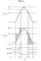
First, the operation when the piezoelectric element 52 a is charged will be described. For convenience, a case in which the piezoelectric element 52 a is controlled by using a voltage waveform signal COM′ having a trapezoidal voltage change pattern will be described, as shown in FIG. 3.
During a period from a timing t0 to a timing t1, the printer-side controller 70 outputs DAC data at a voltage V1 to the waveform generating circuit 41. Accordingly, the waveform generating circuit 41 outputs a voltage waveform signal COM′ at a voltage V1 during the corresponding period. The voltage waveform signal COM′ is input to the base of the first NPN transistor 44 b in the first selection circuit 44. Here, the voltage V1 is sufficiently lower than the voltage (24 V) to be supplied from the capacitor 43. For this reason, in the first selection circuit 44, the first NPN transistor 44 b and the first PNP transistor 44 a are both turned off. Then, as indicated by a bold line in FIG. 4, the charge accumulated in the capacitor 43 is supplied to the collector of the NPN transistor 42 a in the current amplifying circuit 42 through the first diode 44 c. That is, the collector of the NPN transistor 42 a is substantially at 24V. Moreover, the NPN transistor 42 a is turned off during the corresponding period. This is because the emitter voltage (the voltage of the driving signal COM) and the base voltage (the voltage of the voltage waveform signal COM′) in the NPN transistor 42 a are substantially equal to each other.
During a period from the timing t1 to a timing t4, the printer-side controller 70 updates the contents of the DAC data so as to increase the voltage of the voltage waveform signal COM′ by a predetermined value. Accordingly, the voltage of the voltage waveform signal COM′, which is the voltage V1 at the timing t1, becomes a voltage V4 at the timing t4. Then, the NPN transistor 42 a in the current amplifying circuit 42 also operates to amplify the current of the voltage waveform signal COM′ and output the amplified signal as the driving signal COM. That is, the NPN transistor 42 a pushes the current to the piezoelectric element 52 a. The piezoelectric element 52 a is charged with the pushed current.
Here, during a period until the voltage of the voltage waveform signal COM′ reaches a predetermined voltage (a voltage higher than the voltage supplied from the capacitor 43 by 0.6 V), that is, a period from the timing t1 to t3, the transistors 44 a and 44 b in the first selection circuit 44 are kept turned off. For this reason, the capacitor 43 serving as a second current source is connected to the collector of the NPN transistor 42 a in the current amplifying circuit 42 through the first diode 44 c. Therefore, the charge accumulated in the capacitor 43 is used to amplify the current during the corresponding period.
If the voltage of the voltage waveform signal COM′ becomes equal to or more than the predetermined voltage, the transistors 44 a and 44 b in the first selection circuit 44 are turned on. Specifically, the transistors 44 a and 44 b are turned on during a period from the timing t3 to a timing t6. Accordingly, as indicated by a bold line in FIG. 5, the first power generating circuit 81 is connected to the collector of the NPN transistor 42 a in the current amplifying circuit 42 through the first PNP transistor 44 a. Then, during a period from the timing t3 to the timing t4, the current of the voltage waveform signal COM′ is amplified. In this amplification, the first power supply voltage is used.
Here, power consumption of the NPN transistor 42 a in the current amplifying circuit 42 will be described. Power consumption can be represented as a product of a difference in voltage between the collector and the emitter of the NPN transistor 42 a and the amplified current. As described above, during the period from the timing t1 to the timing t3, the current is amplified by using the charge accumulated in the capacitor 43, and during the period from the timing t3 to the timing t4, the current is amplified by using the first power supply voltage. The difference in voltage between the collector and the emitter of the NPN transistor 42 a is indicated by a hatched region in the middle of FIG. 3. By multiplying the voltage difference by a push current supplied to the piezoelectric element 52 a, power consumption of the NPN transistor 42 a is calculated. In the example shown in FIG. 3, the current source is switched at the timing t3. Therefore, it can be seen that power consumption can be suppressed, compared with a case in which a single power supply voltage (for example, 42 V) is used. That is, during the period from the timing t1 to the timing t3, since the current source operates at 24 V, the voltage difference can be reduced by the amount corresponding to the difference in the case in which the single power supply voltage is used.
The first selection circuit 44 uses, as switching elements, two transistors (first PNP transistor 44 a and first NPN transistor 44 b) for switching the current source. That is, during the turned-on state, the collector voltage and the emitter voltage are substantially equalized. Accordingly, power consumption can be suppressed so as to be sufficiently low. In addition, the first diode 44 c which is provided between the capacitor 43 and the NPN transistor 42 a has sufficiently low power consumption. Therefore, a countermeasure against heat generation, such as a heat sink, does not need to be provided for these elements, and thus the apparatus can be compact. With respect to the NPN transistor 42 a in the current amplifying circuit 42, power consumption can be suppressed by switching of the current source. Therefore, a small heat sink can be used, compared with the related art.
Regarding Operation During Discharging
Next, the operation when the piezoelectric element 52 a is discharged will be described. During a period from a timing t5 to a timing t8, the printer-side controller 70 updates the contents of the DAC data so as to decrease the voltage of the voltage waveform signal COM′ by a predetermined value. Accordingly, the voltage of the voltage waveform signal COM′, which is the voltage V4 at the timing t5, becomes the voltage V1 at the timing t8.
Then, the PNP transistor 42 b in the current amplifying circuit 42 also operates to amplify the current of the voltage waveform signal COM′ and outputs the amplified signal as the driving signal COM. That is, the PNP transistor 42 b pulls a current from the piezoelectric element 52 a. The piezoelectric element 52 a is discharged by pulling of the current. Here, during a period until the voltage of the voltage waveform signal COM′ reaches a predetermined voltage (a voltage lower than the voltage supplied from the capacitor 43 by 0.6 V), that is, a period from the timing t5 to the timing t7, the transistors 45 a and 45 b in the second selection circuit 45 are kept turned off. For this reason, the capacitor 43 serving as a second charge emission destination is connected to the collector of the PNP transistor 42 b in the current amplifying circuit 42 through the second diode 45 c. Accordingly, as indicated by a bold line in FIG. 6, the charge is emitted from the collector of the PNP transistor 42 b to the capacitor 43 through the second diode 45 c. The charge is accumulated in the capacitor 43. The charge accumulated in the capacitor 43 is used when the piezoelectric element 52 a is charged. Moreover, second power generating circuit 82 is connected to the positive terminal of the capacitor 43, but the current is limited by the resistor 82 a. Therefore, the charge to be moved when the piezoelectric element 52 a is discharged can be accumulated in the capacitor 43.
If the voltage of the voltage waveform signal COM′ is equal to or less than the predetermined voltage, the transistors 45 a and 45 b in the second selection circuit 45 are turned on. Specifically, during the period from the timing t7 to the timing t8, the transistors 45 a and 45 b are turned on. Accordingly, as indicated by a bold line in FIG. 7, the ground is connected to the collector of the PNP transistor 42 b in the current amplifying circuit 42 through the second NPN transistor 45 a. Therefore, during the period from the timing t7 to the timing t8, although the current of the voltage waveform signal COM′ is amplified, the charge from the piezoelectric element 52 a is emitted to the ground.
Here, power consumption of the PNP transistor 42 b in the current amplifying circuit 42 will be described. Power consumption can be represented as a product of a difference in voltage between the collector and the emitter of the PNP transistor 42 b and the amplified current. As described above, during the period from the timing t5 to the timing t7, the positive terminal of the capacitor 43 is connected to the collector of the PNP transistor 42 b through the second diode 45 c. In addition, during the period from the timing t7 to the timing t8, the ground is connected to the collector of the PNP transistor 42 b through the second NPN transistor 45 a. For this reason, the charge from the piezoelectric element 52 a is emitted to the capacitor 43 during the period from the timing t5 to the timing t7, and is emitted to the ground during the period from the timing t7 to the timing t8.
The difference in voltage between the collector and the emitter in the PNP transistor 42 b is indicated by a hatched region in the middle of FIG. 3. By multiplying the voltage difference by the pull current from the piezoelectric element 52 a, power consumption of the PNP transistor 42 b is calculated. In the example shown in FIG. 3, the charge emission destination is switched at the timing t7. Accordingly, it can be seen that power consumption can be suppressed, compared with a case in which the ground only serves as a charge emission destination. That is, during the period from the timing t5 to the timing t7, since the charge emission destination is at 24 V, the voltage difference can be reduced by the difference from a case in which the ground is only used.
The second selection circuit 45 also uses, as switching elements, two transistors (second NPN transistor 45 a and second PNP transistor 45 b) for switching the charge emission destination. Accordingly, power consumption can be suppressed so as to be sufficiently low. In addition, the second diode 45 c which is provided between the capacitor 43 and the PNP transistor 42 b has sufficiently low power consumption. Therefore, a countermeasure against heat generation, such as a heat sink, does not need to be provided for these elements, and thus the apparatus can be compact. With respect to the PNP transistor 42 b in the current amplifying circuit 42, power consumption can be suppressed by switching of the current source. Therefore, a small heat sink can be used, compared with the related art.
Conclusion of First Embodiment
As will be apparent from the above description, in the printer 1 according to the first embodiment, the first selection circuit 44 selectively connects a plurality of current sources at different voltages (the first power generating circuit 81 and the capacitor 43) to the collector of the NPN transistor 42 a (a charging transistor of the piezoelectric element 52 a) in the current amplifying circuit 42. Accordingly, a current source suitable for the voltage of the voltage waveform signal can be used, and power consumption of the NPN transistor 42 a can be suppressed. Therefore, a heat sink can be compact. Furthermore, a transistor package having low power consumption may be used.
When selecting a plurality of current sources, the first selection circuit 44 uses, as switching elements, bipolar transistors (the first PNP transistor 44 a and the first NPN transistor 44 b). For this reason, heat generation during the operation can be suppressed, and a heat sink can be removed, thereby making the apparatus compact.
The first selection circuit 44 connects a current source at a lower voltage (the capacitor 43) to the collector of the NPN transistor 42 a through the first diode 44 c, and connects a current source at a higher voltage (the first power generating circuit 81) to the collector of the NPN transistor 42 a through the current source switch (the first PNP transistor 44 a). Accordingly, by controlling the current source switch, a current source to be connected to the collector of the NPN transistor 42 a can be selected. Therefore, the configuration can be simplified and the control can be easily performed.
The second selection circuit 45 selectively connects a plurality of charge emission destinations at different voltages (the ground and the capacitor 43) to the collector of the PNP transistor 42 b (a discharging transistor of the piezoelectric element 52 a) in the current amplifying circuit 42. Therefore, power consumption of the PNP transistor 42 b can be suppressed, and a heat sink can be compact. Furthermore, a transistor package having low power consumption can be used.
When selecting a plurality of charge emission destinations, the second selection circuit 45 uses bipolar transistors (the second NPN transistor 45 a and the second PNP transistor 45 b) as switching elements. Therefore, heat generation during the operation can be suppressed, and a heat sink can be removed, thereby making the apparatus compact.
The second selection circuit 45 connects a charge emission destination at a higher voltage (the capacitor 43) to the collector of the PNP transistor 42 b through the second diode 45 c, and connects a charge emission destination at a lower voltage (the ground) to the collector of the PNP transistor 42 b through the charge emission destination switch (the second NPN transistor 45 a). Accordingly, by controlling the charge emission destination switch, a charge emission destination to be connected to the collector of the PNP transistor 42 b can be selected. Therefore, the configuration can be simplified, and the control can be easily performed.
With respect to the current sources, the printer 1 uses the first power generating circuit 81 (a power supply circuit) as a first current source at a higher voltage, and uses the capacitor 43 as a second current source at a lower voltage. Accordingly, even if the charge accumulated in the capacitor 43 is consumed and charge supply becomes difficult, a charge can be supplied from the first power generating circuit 81. Therefore, the reliability can be improved.
SECOND EMBODIMENT
In the printer 1 according to the first embodiment, as shown in FIG. 3, if the voltage of the voltage waveform signal COM′ is higher than the voltage (24 V) supplied from the capacitor 43 by 0.6 V or more (t3 to t6), the first power generating circuit 81 is selected as a current source. If the voltage of the voltage waveform signal COM′ is lower than the voltage supplied from the capacitor 43 by 0.6 V or more (t0 to t2, t7 and later), the ground is selected as a charge emission destination. In this case, though for a very short time, when the piezoelectric element 52 a is charged, the voltage of the voltage waveform signal COM′ becomes higher than the voltage of the current source. In addition, when the piezoelectric element 52 a is discharged, the voltage of the voltage waveform signal COM′ becomes lower than the voltage of the charge emission destination. Accordingly, the voltage change pattern of the driving signal COM may be distorted.
The second embodiment has been made in consideration of this problem, and is designed to optimize switching of a current source or a charge emission destination. FIG. 8 is a diagram illustrating a driving signal generating circuit 40 in a printer 1 according to the second embodiment. Moreover, other parts of the printer 1 are the same as those in the first embodiment, and thus the descriptions thereof will be omitted. In the second embodiment, similarly to the first embodiment, a driving signal generating circuit 40 has a waveform generating circuit 41, a current amplifying circuit 42, a capacitor 43, a first selection circuit 44, and a second selection circuit 45. Of these, the waveform generating circuit 41, the current amplifying circuit 42, and the capacitor 43 have the same configuration as those in the first embodiment.
Regarding First Selection Circuit 44
The first selection circuit 44 has the following differences from that in the first embodiment. That is, a first FET 44 f, instead of the first PNP transistor 44 a, is used as a current source switch, and a first Zener diode 44 g is provided between a base of a first NPN transistor 44 b and a resistor 44 e. In addition, an emitter of the first NPN transistor 44 b is connected to the ground.
The first FET 44 f has the same function as the first PNP transistor 44 a. That is, the first FET 44 f selectively connects the first power generating circuit 81 to the collector of the NPN transistor 42 a in the current amplifying circuit 42. A cathode of the first Zener diode 44 g is connected to the supply line of the voltage waveform signal COM′ through the resistor 44 e, and an anode of the first Zener diode 44 g is connected to the base of the first NPN transistor 44 b. The first Zener diode 44 g is an element for controlling the operation of the first NPN transistor 44 b. Specifically, the first Zener diode 44 g blocks application of the voltage waveform signal COM′ to the first NPN transistor 44 b when a difference between the voltage of the voltage waveform signal COM′ and the base voltage of the first NPN transistor 44 b is less than a Zener voltage. Meanwhile, when the difference between the voltage of the voltage waveform signal COM′ and the base voltage of the first NPN transistor 44 b is equal to or more than the Zener voltage, the first Zener diode 44 g allows application of the voltage waveform signal COM′ to the first NPN transistor 44 b.
In the first selection circuit 44 having the above configuration, when the voltage waveform signal COM′ is at a low voltage, and the difference between the voltage of the voltage waveform signal COM′ and the base voltage of the first NPN transistor 44 b is less than the Zener voltage, the first NPN transistor 44 b is turned off. Then, a gate voltage is at H level, and the first FET 44 f is also turned off. Accordingly, the capacitor 43 is connected to the collector of the NPN transistor 42 a in the current amplifying circuit 42 through the first diode 44 c.
If the voltage of the voltage waveform signal COM′ increases and becomes more than the base voltage of the first NPN transistor 44 b by the Zener voltage or more, the first Zener diode 44 g is conducted. Then, the base voltage of the first NPN transistor 44 b is substantially equalized to the voltage of the voltage waveform signal COM′, and the first NPN transistor 44 b is turned on. That is, the collector and the emitter are conducted. Accordingly, the gate voltage of the first FET 44 f decreases and is at L level, the source and the drain are conducted. As a result, the first power generating circuit 81 is connected to the collector of the NPN transistor 42 a in the current amplifying circuit 42 through the first FET 44 f.
In this way, the first Zener diode 44 g and the first NPN transistor 44 b function as a control circuit for controlling the operation of the first FET 44 f. The control circuit outputs a control signal at H level to the gate of the first FET 44 f when the voltage of the voltage waveform signal COM′ is less than a predetermined voltage, and connects the capacitor 43 to the NPN transistor 42 a. When the voltage of the voltage waveform signal COM′ is equal to or more than the predetermined voltage, the control circuit outputs a control signal at L level to the gate of the first FET 44 f, and connects the first power generating circuit 81 to the NPN transistor 42 a.
Regarding Second Selection Circuit 45
The second selection circuit 45 has the following differences from that in the first embodiment. That is, a second FET 45 f, instead of the second NPN transistor 45 a, is used as a charge emission destination switch, and a second Zener diode 45 g is provided between a base of a second PNP transistor 45 b and a resistor 45 e. In addition, an emitter of the second PNP transistor 45 b is connected to the first power generating circuit 81.
The second FET 45 f has the same function as the second NPN transistor 45 a. That is, the second FET 45 f selectively connects the ground to the collector of the PNP transistor 42 b in the current amplifying circuit 42. An anode of the second Zener diode 45 g is connected to the supply line of the voltage waveform signal COM′ through the resistor 45 e, and a cathode of the second Zener diode 45 g is connected to the base of the second PNP transistor 45 b. The second Zener diode 45 g is an element for controlling the operation of the second PNP transistor 45 b. Specifically, the second Zener diode 45 g blocks application of the voltage waveform signal COM′ to the second PNP transistor 45 b when a difference between the voltage of the voltage waveform signal COM′ and the base voltage of the second PNP transistor 45 b is less than a Zener voltage. Meanwhile, when the difference between the voltage of the voltage waveform signal COM′ and the base voltage of the second PNP transistor 45 b is equal to or more than the Zener voltage, the second Zener diode 45 g allows application of the voltage waveform signal COM′ to the second PNP transistor 45 b.
In the second selection circuit 45 having the above configuration, when the voltage waveform signal COM′ is at a high voltage, and the difference between the voltage of the voltage waveform signal COM′ and the base voltage of the second PNP transistor 45 b is less than the Zener voltage, the second PNP transistor 45 b is turned off. Then, a gate voltage is at L level, and the second FET 45 f is also turned off. Accordingly, the capacitor 43 is connected to the collector of the PNP transistor 42 b in the current amplifying circuit 42 through the second diode 45 c.
If the voltage of the voltage waveform signal COM′ decreases and is less than the base voltage of the second PNP transistor 45 b by the Zener voltage or more, the second Zener diode 45 g is conducted. Then, the base voltage of the second PNP transistor 45 b is substantially equalized to the voltage of the voltage waveform signal COM′, and the second PNP transistor 45 b is turned on. That is, the collector and the emitter are conducted. Accordingly, the gate voltage of the second FET 45 f increases and is at H level, and the source and the drain are conducted. As a result, the ground is connected to the collector of the PNP transistor 42 b in the current amplifying circuit 42 through the second FET 45 f.
In this way, the second Zener diode 45 g and the second PNP transistor 45 b function as a control circuit for controlling the operation of the second FET 45 f. The control circuit outputs a control signal at L level to the gate of the second FET 45 f when the voltage of the voltage waveform signal COM′ is more than a predetermined voltage, and connects the capacitor 43 to the PNP transistor 42 b. When the voltage of the voltage waveform signal COM′ is equal to or less than the predetermined voltage, the control circuit outputs a control signal at H level to the gate of the second FET 45 f, and connects the ground to the PNP transistor 42 b.
Regarding Driving Signal COM to be Generated
In the driving signal generating circuit 40 according to the second embodiment, by appropriately setting the Zener voltage of the first Zener diode 44 g or the second Zener diode 45 g, the switching timing of the current source or the switching timing of the charge emission destination can be determined. In the example shown in FIG. 9, when the piezoelectric element 52 a is charged, at a timing t2 immediately before the voltage of the voltage waveform signal COM′ reaches 24 V, which is the voltage of the capacitor 43, the current source can be switched to the first power generating circuit 81. Similarly, when the piezoelectric element 52 a is discharged, at a timing t6 immediately before the voltage of the voltage waveform signal COM′ reaches 24 V, the charge emission destination can be switched to the ground.
Therefore, the current source or the charge emission destination can be switched at an appropriate timing, and distortion of the driving signal COM can be suppressed.
OTHER EMBODIMENTS
The foregoing embodiments have described the printing system having the printer 1, but they also include the disclosure of a liquid ejecting method. In addition, the foregoing embodiments are for the purpose of facilitating understanding the invention, and are not to be interpreted as limiting the invention. The invention can of course be altered and improved without departing from the gist thereof, and includes functional equivalents. In particular, the following embodiments are also included in the invention.
Regarding Current Amplifying Transistor
In the foregoing embodiments, the NPN transistor 42 a and the PNP transistor 42 b are illustrated as the charging transistor and the discharging transistor in the current amplifying circuit 42, respectively. However, any transistor may be used insofar as it can amplify the current of the voltage waveform signal COM′ (analog signal).
Regarding Current Source or Charge Emission Destination
In the foregoing embodiments, a case in which a plurality of current sources or charge emission destinations at different voltages are selected has been described, current sources or charge emission destinations at the same voltage may be selected. Furthermore, with respect to the current source or the charge emission destination, the voltage is switched in two steps, but the voltage may be switched in three or more steps.
Regarding Driving Signal COM
In the foregoing embodiments, a case in which the printer 1 generates the single driving signal COM has been described, but the invention can be similarly to a printer 1 that generates a plurality of driving signals COM. That is, although a plurality of driving signals COM are generated, and required segments of the driving signals COM are selectively applied to the piezoelectric element 52 a, the same advantages and effects can be obtained.
Regarding Other Apparatuses
In the foregoing embodiments, the printer 1 in which the head 52 is moved along with the carriage has been described, but the invention may be applied to a so-called line printer.
In the forgoing embodiments, the printer 1 has been described as a liquid ejecting apparatus, but the invention is not limited to the printer 1. For example, technology like that of the embodiments can also be applied to various apparatuses that employ ink jet technology, such as a color filter manufacturing apparatus, a dyeing apparatus, a fine processing apparatus, a semiconductor manufacturing apparatus, a surface processing apparatus, a three-dimensional shape forming machine, a liquid vaporizing apparatus, an organic EL manufacturing apparatus (in particular, a macromolecular EL manufacturing apparatus), a display manufacturing apparatus, a film forming apparatus, and a DNA chip manufacturing apparatus. Also, methods therefor and manufacturing methods thereof are within the scope of application.

Claims (13)

1. A liquid ejecting apparatus, comprising:
an element that is charged and discharged so as to perform an operation to eject a liquid;
an analog signal generating unit that generates an analog signal having a voltage change pattern for determining the operation of the element;
a charging transistor that amplifies a current of the analog signal while the element is charged, and pushes the amplified current toward the element, the charging transistor having a current source terminal, to which a current source is connected, and a push terminal for pushing the current;
a current source connector that selects at least one current source from among a plurality of current sources according to a voltage of the analog signal, and connects the selected current source to the current source terminal,
wherein the current source connector selects at least one current source from among the plurality of current sources at different voltages,
wherein the plurality of current sources have a first current source at a first voltage and a second current source at a second voltage lower than the first voltage, and
the current source connector includes:
a current source switch that is provided between the first current source and the current source terminal, and
a control circuit that outputs, to the current source switch, a control signal at a voltage level determined to control the operation of the current source switch on the basis of the voltage of the analog signal.
2. The liquid ejecting apparatus according to claim 1, wherein the current source connector switches a current source to be selected while the element is charged.
3. The liquid ejecting apparatus according to claim 1, wherein the plurality of current sources have a first current source at a first voltage and a second current source at a second voltage lower than the first voltage, and
the current source connector includes
a current source switch that is provided between the first current source and the current source terminal, and
an element that is provided between the second current source and the current source terminal, and allows charge movement from the second current source to the current source terminal, while blocking charge movement from the current source terminal to the second current source.
4. The liquid ejecting apparatus according to claim 1, wherein the current source switch has a transistor.
5. The liquid ejecting apparatus according to 1, wherein the first current source has a power supply circuit, and
the second current source has a capacitor.
6. The liquid ejecting apparatus according to claim 5, wherein the capacitor is charged with a charge to be moved while the element is discharged.
7. The liquid ejecting apparatus according to claim 6, further comprising:
a discharging transistor that amplifies the current of the analog signal while the element is discharged, and pulls the current from the element, the discharging transistor having a pull terminal for pulling the current and an emission terminal for emitting the charge; and
a charge emission destination connector that selects at least one charge emission destination from among a plurality of charge emission destinations including the capacitor according to the voltage of the analog signal, and connects the selected charge emission destination to the emission terminal.
8. The liquid ejecting apparatus according to claim 6, wherein the second current source emits the charge accumulated in the capacitor while the element is charged.
9. A liquid ejecting apparatus, comprising:
an element that is charged and discharged so as to perform an operation to eject a liquid;
an analog signal generating unit that generates an analog signal having a voltage change pattern for determining the operation of the element;
a discharging transistor that amplifies the current of the analog signal while the element is discharged, and pulls the current from the element, the discharging transistor having a pull terminal for pulling the current and an emission terminal for emitting the charge; and
a charge emission destination connector that selects at least one charge emission destination from among a plurality of charge emission destinations according to the voltage of the analog signal, and connects the selected charge emission destination to the emission terminal,
wherein the charge emission destination connector selects at least one charge emission destination from among a plurality of charge emission destinations at different voltages,
wherein the plurality of charge emission destinations have a first charge emission destination at a first voltage, and a second charge emission destination at a second voltage higher than the first voltage, and
the charge emission destination connector includes:
a charge emission destination switch that is provided between the emission terminal and the first charge emission destination, and
a control circuit that outputs, to the charge emission destination switch, a control signal at a voltage level determined to control the operation of the charge emission destination switch on the basis of the voltage of the analog signal.
10. The liquid ejecting apparatus according to claim 8,
wherein the charge emission destination connector switches a charge emission destination to be selected while the element is discharged.
11. The liquid ejecting apparatus according to claim 10,
wherein the first charge emission destination is the ground,
and the second charge emission destination is a capacitor.
12. The liquid ejecting apparatus according to claim 11,
wherein the plurality of charge emission destinations have a first charge emission destination at a first voltage, and a second charge emission destination at a second voltage higher than the first voltage, and
the charge emission destination connector includes a charge emission destination switch that is provided between the emission terminal and the first charge emission destination, and
element that is provided between the emission terminal and the second charge emission destination, and allows charge movement from the emission terminal to the second charge emission destination, while blocking charge movement from the second charge emission destination to the emission terminal.
13. The liquid ejecting apparatus according to claim 9,
wherein the charge emission destination switch is a transistor.
US12/145,725 2007-06-26 2008-06-25 Liquid ejecting apparatus and liquid ejecting method Active 2029-10-13 US8083309B2 (en)

Applications Claiming Priority (2)

Application Number Priority Date Filing Date Title
JP2007-167802 2007-06-26
JP2007167802A JP4983434B2 (en) 2007-06-26 2007-06-26 Liquid ejection apparatus and liquid ejection method

Publications (2)

Publication Number Publication Date
US20090002036A1 US20090002036A1 (en) 2009-01-01
US8083309B2 true US8083309B2 (en) 2011-12-27

Family

ID=40159647

Family Applications (1)

Application Number Title Priority Date Filing Date
US12/145,725 Active 2029-10-13 US8083309B2 (en) 2007-06-26 2008-06-25 Liquid ejecting apparatus and liquid ejecting method

Country Status (2)

Country Link
US (1) US8083309B2 (en)
JP (1) JP4983434B2 (en)

Cited By (1)

* Cited by examiner, † Cited by third party
Publication number Priority date Publication date Assignee Title
US20150197083A1 (en) * 2014-01-16 2015-07-16 Seiko Epson Corporation Liquid discharge apparatus, head unit, and control method of liquid discharge apparatus

Families Citing this family (8)

* Cited by examiner, † Cited by third party
Publication number Priority date Publication date Assignee Title
WO2010052132A1 (en) * 2008-11-05 2010-05-14 Oce-Technologies B.V. A driver circuit for driving a print head of an inkjet printer
JP5407518B2 (en) * 2009-04-23 2014-02-05 セイコーエプソン株式会社 Drive signal generation circuit and drive signal generation method
JP5564855B2 (en) * 2009-08-25 2014-08-06 セイコーエプソン株式会社 Liquid ejecting apparatus and liquid ejecting method
JP5760708B2 (en) 2011-06-01 2015-08-12 株式会社リコー Image forming apparatus and drive voltage generation circuit
JP6088150B2 (en) * 2012-04-06 2017-03-01 エスアイアイ・プリンテック株式会社 Drive device, liquid jet head, liquid jet recording apparatus, and drive method
US9455697B2 (en) * 2012-09-28 2016-09-27 Infineon Technologies Austria Ag Switch circuit with a first transistor device and a second transistor device connected in series
US9793260B2 (en) * 2015-08-10 2017-10-17 Infineon Technologies Austria Ag System and method for a switch having a normally-on transistor and a normally-off transistor
JP7142590B2 (en) * 2019-03-01 2022-09-27 東芝テック株式会社 DRIVE CIRCUIT OF LIQUID EJECTOR AND LIQUID EJECTOR

Citations (11)

* Cited by examiner, † Cited by third party
Publication number Priority date Publication date Assignee Title
JPH08300646A (en) 1994-07-01 1996-11-19 Seiko Epson Corp Ink-jet recording device
JPH11170529A (en) 1997-10-09 1999-06-29 Seiko Epson Corp Capacitive load driving circuit and recording head driving circuit
JP2000103055A (en) 1998-09-30 2000-04-11 Brother Ind Ltd Drive circuit of ink jet head
JP2000238264A (en) 1999-02-18 2000-09-05 Seiko Epson Corp Capacitive load driving circuit
JP2001150666A (en) 1999-11-24 2001-06-05 Matsushita Electric Ind Co Ltd Driving circuit for ink-jet head
US6364444B1 (en) * 1999-05-06 2002-04-02 Nec Corporation Apparatus for and method of driving ink-jet recording head for controlling amount of discharged ink drop
US6382754B1 (en) * 1995-04-21 2002-05-07 Seiko Epson Corporation Ink jet printing device
JP2004306434A (en) 2003-04-07 2004-11-04 Seiko Epson Corp Head driver of ink jet printer
JP2005169737A (en) 2003-12-09 2005-06-30 Ricoh Co Ltd Driving waveform generating circuit, driving waveform generating method and image forming apparatus
JP2005254644A (en) 2004-03-12 2005-09-22 Seiko Epson Corp Print head drive circuit
US7744182B2 (en) * 2005-10-05 2010-06-29 Fuji Xerox Co., Ltd. Capacitive load driving circuit and method, and liquid drop ejecting device

Patent Citations (11)

* Cited by examiner, † Cited by third party
Publication number Priority date Publication date Assignee Title
JPH08300646A (en) 1994-07-01 1996-11-19 Seiko Epson Corp Ink-jet recording device
US6382754B1 (en) * 1995-04-21 2002-05-07 Seiko Epson Corporation Ink jet printing device
JPH11170529A (en) 1997-10-09 1999-06-29 Seiko Epson Corp Capacitive load driving circuit and recording head driving circuit
JP2000103055A (en) 1998-09-30 2000-04-11 Brother Ind Ltd Drive circuit of ink jet head
JP2000238264A (en) 1999-02-18 2000-09-05 Seiko Epson Corp Capacitive load driving circuit
US6364444B1 (en) * 1999-05-06 2002-04-02 Nec Corporation Apparatus for and method of driving ink-jet recording head for controlling amount of discharged ink drop
JP2001150666A (en) 1999-11-24 2001-06-05 Matsushita Electric Ind Co Ltd Driving circuit for ink-jet head
JP2004306434A (en) 2003-04-07 2004-11-04 Seiko Epson Corp Head driver of ink jet printer
JP2005169737A (en) 2003-12-09 2005-06-30 Ricoh Co Ltd Driving waveform generating circuit, driving waveform generating method and image forming apparatus
JP2005254644A (en) 2004-03-12 2005-09-22 Seiko Epson Corp Print head drive circuit
US7744182B2 (en) * 2005-10-05 2010-06-29 Fuji Xerox Co., Ltd. Capacitive load driving circuit and method, and liquid drop ejecting device

Cited By (3)

* Cited by examiner, † Cited by third party
Publication number Priority date Publication date Assignee Title
US20150197083A1 (en) * 2014-01-16 2015-07-16 Seiko Epson Corporation Liquid discharge apparatus, head unit, and control method of liquid discharge apparatus
US9505210B2 (en) * 2014-01-16 2016-11-29 Seiko Epson Corporation Liquid discharge apparatus, head unit, and control method of liquid discharge apparatus
US9764547B2 (en) 2014-01-16 2017-09-19 Seiko Epson Corporation Driving circuit for driving a capacitive load

Also Published As

Publication number Publication date
JP4983434B2 (en) 2012-07-25
JP2009006505A (en) 2009-01-15
US20090002036A1 (en) 2009-01-01

Similar Documents

Publication Publication Date Title
US8083309B2 (en) Liquid ejecting apparatus and liquid ejecting method
US20080238964A1 (en) Drive signal generating apparatus, liquid ejecting apparatus, and drive signal generating method
US7625056B2 (en) Device and method for driving jetting head
JP5163207B2 (en) Liquid ejecting apparatus and printing apparatus
JP5760708B2 (en) Image forming apparatus and drive voltage generation circuit
JP5034752B2 (en) Drive signal generator
JP4984006B2 (en) Drive signal generation circuit
JP3757808B2 (en) Ink jet printer head drive apparatus and drive method
US7638992B2 (en) Drive power control device, liquid ejection apparatus, and drive power control method
JP2002273874A (en) Device and method for driving head of ink-jet printer
JP2011046028A (en) Liquid jetting apparatus and liquid jetting method
JP4670298B2 (en) Drive signal generation method, printing apparatus, and printing system
JP2010135942A (en) Charge and discharge circuit of capacitive load
JP2011050132A (en) Liquid discharge device and liquid discharge method
JP2010253698A (en) Drive signal generating circuit, and fluid jetting apparatus
JP2011046030A (en) Liquid jetting apparatus and liquid jetting method
JP2003300318A (en) Head driver of ink jet printer
JP5564855B2 (en) Liquid ejecting apparatus and liquid ejecting method
US11376844B2 (en) Drive circuit and liquid ejecting apparatus
US8702191B2 (en) Printer control method and system
JP2011046027A (en) Liquid jetting apparatus and liquid jetting method
JP2006205391A (en) Liquid ejecting apparatus, and liquid ejection method
JP5440684B2 (en) Driving circuit
JP2010135943A (en) Charge and discharge circuit of capacitive load
JP2011047295A (en) Liquid jetting device and liquid jetting method

Legal Events

Date Code Title Description
AS Assignment

Owner name: SEIKO EPSON CORPORATION, JAPAN

Free format text: ASSIGNMENT OF ASSIGNORS INTEREST;ASSIGNOR:UMEDA, ATSUSHI;REEL/FRAME:021149/0012

Effective date: 20080527

FEPP Fee payment procedure

Free format text: PAYOR NUMBER ASSIGNED (ORIGINAL EVENT CODE: ASPN); ENTITY STATUS OF PATENT OWNER: LARGE ENTITY

STCF Information on status: patent grant

Free format text: PATENTED CASE

FPAY Fee payment

Year of fee payment: 4

MAFP Maintenance fee payment

Free format text: PAYMENT OF MAINTENANCE FEE, 8TH YEAR, LARGE ENTITY (ORIGINAL EVENT CODE: M1552); ENTITY STATUS OF PATENT OWNER: LARGE ENTITY

Year of fee payment: 8

MAFP Maintenance fee payment

Free format text: PAYMENT OF MAINTENANCE FEE, 12TH YEAR, LARGE ENTITY (ORIGINAL EVENT CODE: M1553); ENTITY STATUS OF PATENT OWNER: LARGE ENTITY

Year of fee payment: 12