US8080826B1 - High performance active and passive structures based on silicon material bonded to silicon carbide - Google Patents
High performance active and passive structures based on silicon material bonded to silicon carbide Download PDFInfo
- Publication number
- US8080826B1 US8080826B1 US10/656,613 US65661303A US8080826B1 US 8080826 B1 US8080826 B1 US 8080826B1 US 65661303 A US65661303 A US 65661303A US 8080826 B1 US8080826 B1 US 8080826B1
- Authority
- US
- United States
- Prior art keywords
- semiconductor material
- single crystal
- silicon carbide
- layer
- crystal silicon
- Prior art date
- Legal status (The legal status is an assumption and is not a legal conclusion. Google has not performed a legal analysis and makes no representation as to the accuracy of the status listed.)
- Expired - Fee Related, expires
Links
- HBMJWWWQQXIZIP-UHFFFAOYSA-N silicon carbide Chemical group [Si+]#[C-] HBMJWWWQQXIZIP-UHFFFAOYSA-N 0.000 title claims abstract description 291
- 229910010271 silicon carbide Inorganic materials 0.000 title claims abstract description 289
- 239000002210 silicon-based material Substances 0.000 title description 5
- 239000000463 material Substances 0.000 claims abstract description 236
- 239000004065 semiconductor Substances 0.000 claims abstract description 192
- 239000000758 substrate Substances 0.000 claims abstract description 155
- XUIMIQQOPSSXEZ-UHFFFAOYSA-N Silicon Chemical group [Si] XUIMIQQOPSSXEZ-UHFFFAOYSA-N 0.000 claims abstract description 94
- 229910000577 Silicon-germanium Inorganic materials 0.000 claims abstract description 56
- 229910052710 silicon Inorganic materials 0.000 claims abstract description 55
- 239000010703 silicon Substances 0.000 claims abstract description 55
- 238000000926 separation method Methods 0.000 claims abstract description 37
- VYPSYNLAJGMNEJ-UHFFFAOYSA-N Silicium dioxide Chemical compound O=[Si]=O VYPSYNLAJGMNEJ-UHFFFAOYSA-N 0.000 claims abstract description 29
- LEVVHYCKPQWKOP-UHFFFAOYSA-N [Si].[Ge] Chemical compound [Si].[Ge] LEVVHYCKPQWKOP-UHFFFAOYSA-N 0.000 claims abstract description 23
- 229910052799 carbon Inorganic materials 0.000 claims abstract description 13
- 229910017052 cobalt Inorganic materials 0.000 claims abstract description 13
- 239000010941 cobalt Substances 0.000 claims abstract description 13
- GUTLYIVDDKVIGB-UHFFFAOYSA-N cobalt atom Chemical compound [Co] GUTLYIVDDKVIGB-UHFFFAOYSA-N 0.000 claims abstract description 13
- 229910021332 silicide Inorganic materials 0.000 claims abstract description 13
- FVBUAEGBCNSCDD-UHFFFAOYSA-N silicide(4-) Chemical compound [Si-4] FVBUAEGBCNSCDD-UHFFFAOYSA-N 0.000 claims abstract description 13
- 229910021342 tungsten silicide Inorganic materials 0.000 claims abstract description 13
- OKTJSMMVPCPJKN-UHFFFAOYSA-N Carbon Chemical compound [C] OKTJSMMVPCPJKN-UHFFFAOYSA-N 0.000 claims abstract description 12
- WQJQOUPTWCFRMM-UHFFFAOYSA-N tungsten disilicide Chemical compound [Si]#[W]#[Si] WQJQOUPTWCFRMM-UHFFFAOYSA-N 0.000 claims abstract description 12
- 239000000377 silicon dioxide Substances 0.000 claims abstract description 11
- 235000012239 silicon dioxide Nutrition 0.000 claims abstract description 11
- 230000008878 coupling Effects 0.000 claims abstract description 7
- 238000010168 coupling process Methods 0.000 claims abstract description 7
- 238000005859 coupling reaction Methods 0.000 claims abstract description 7
- 229910021421 monocrystalline silicon Inorganic materials 0.000 claims description 171
- 239000002019 doping agent Substances 0.000 claims description 47
- 238000000034 method Methods 0.000 claims description 47
- 230000008569 process Effects 0.000 claims description 36
- 238000005229 chemical vapour deposition Methods 0.000 claims description 27
- 238000001451 molecular beam epitaxy Methods 0.000 claims description 19
- 229910052751 metal Inorganic materials 0.000 claims description 12
- 239000002184 metal Substances 0.000 claims description 12
- 229910021341 titanium silicide Inorganic materials 0.000 claims description 12
- 229910021420 polycrystalline silicon Inorganic materials 0.000 claims description 6
- ZXEYZECDXFPJRJ-UHFFFAOYSA-N $l^{3}-silane;platinum Chemical compound [SiH3].[Pt] ZXEYZECDXFPJRJ-UHFFFAOYSA-N 0.000 claims description 5
- 239000007769 metal material Substances 0.000 claims description 5
- 229910021339 platinum silicide Inorganic materials 0.000 claims description 5
- 229920005591 polysilicon Polymers 0.000 claims description 5
- 229910052757 nitrogen Inorganic materials 0.000 claims description 4
- 206010010144 Completed suicide Diseases 0.000 abstract 1
- RTAQQCXQSZGOHL-UHFFFAOYSA-N Titanium Chemical compound [Ti] RTAQQCXQSZGOHL-UHFFFAOYSA-N 0.000 abstract 1
- 239000010936 titanium Substances 0.000 abstract 1
- 229910052719 titanium Inorganic materials 0.000 abstract 1
- 238000005516 engineering process Methods 0.000 description 20
- 229910021419 crystalline silicon Inorganic materials 0.000 description 14
- 150000002500 ions Chemical class 0.000 description 13
- 230000037230 mobility Effects 0.000 description 8
- 239000010408 film Substances 0.000 description 7
- 239000003990 capacitor Substances 0.000 description 6
- 239000000969 carrier Substances 0.000 description 6
- 238000004519 manufacturing process Methods 0.000 description 6
- 230000008901 benefit Effects 0.000 description 5
- 238000000151 deposition Methods 0.000 description 5
- GNPVGFCGXDBREM-UHFFFAOYSA-N germanium atom Chemical group [Ge] GNPVGFCGXDBREM-UHFFFAOYSA-N 0.000 description 5
- 238000004544 sputter deposition Methods 0.000 description 5
- 235000012431 wafers Nutrition 0.000 description 5
- IJGRMHOSHXDMSA-UHFFFAOYSA-N Atomic nitrogen Chemical compound N#N IJGRMHOSHXDMSA-UHFFFAOYSA-N 0.000 description 4
- 150000001875 compounds Chemical class 0.000 description 4
- 230000008021 deposition Effects 0.000 description 4
- 238000005498 polishing Methods 0.000 description 4
- ZOXJGFHDIHLPTG-UHFFFAOYSA-N Boron Chemical compound [B] ZOXJGFHDIHLPTG-UHFFFAOYSA-N 0.000 description 3
- 229910052796 boron Inorganic materials 0.000 description 3
- 239000013078 crystal Substances 0.000 description 3
- 229910021488 crystalline silicon dioxide Inorganic materials 0.000 description 3
- 239000007789 gas Substances 0.000 description 3
- 229910052732 germanium Inorganic materials 0.000 description 3
- 239000000203 mixture Substances 0.000 description 3
- 230000004048 modification Effects 0.000 description 3
- 238000012986 modification Methods 0.000 description 3
- 229910052782 aluminium Inorganic materials 0.000 description 2
- XAGFODPZIPBFFR-UHFFFAOYSA-N aluminium Chemical compound [Al] XAGFODPZIPBFFR-UHFFFAOYSA-N 0.000 description 2
- 229910052785 arsenic Inorganic materials 0.000 description 2
- RQNWIZPPADIBDY-UHFFFAOYSA-N arsenic atom Chemical compound [As] RQNWIZPPADIBDY-UHFFFAOYSA-N 0.000 description 2
- 230000015556 catabolic process Effects 0.000 description 2
- 230000008859 change Effects 0.000 description 2
- 230000007547 defect Effects 0.000 description 2
- 238000006731 degradation reaction Methods 0.000 description 2
- ZOCHARZZJNPSEU-UHFFFAOYSA-N diboron Chemical compound B#B ZOCHARZZJNPSEU-UHFFFAOYSA-N 0.000 description 2
- 230000005684 electric field Effects 0.000 description 2
- 238000005530 etching Methods 0.000 description 2
- BHEPBYXIRTUNPN-UHFFFAOYSA-N hydridophosphorus(.) (triplet) Chemical compound [PH] BHEPBYXIRTUNPN-UHFFFAOYSA-N 0.000 description 2
- 230000001590 oxidative effect Effects 0.000 description 2
- 239000002002 slurry Substances 0.000 description 2
- 239000000126 substance Substances 0.000 description 2
- 230000003746 surface roughness Effects 0.000 description 2
- -1 Argon ion Chemical class 0.000 description 1
- 241000511976 Hoya Species 0.000 description 1
- XYFCBTPGUUZFHI-UHFFFAOYSA-N Phosphine Chemical compound P XYFCBTPGUUZFHI-UHFFFAOYSA-N 0.000 description 1
- 229910052581 Si3N4 Inorganic materials 0.000 description 1
- 229910008310 Si—Ge Inorganic materials 0.000 description 1
- 239000012670 alkaline solution Substances 0.000 description 1
- 229910000074 antimony hydride Inorganic materials 0.000 description 1
- XKRFYHLGVUSROY-UHFFFAOYSA-N argon Substances [Ar] XKRFYHLGVUSROY-UHFFFAOYSA-N 0.000 description 1
- 229910052786 argon Inorganic materials 0.000 description 1
- RBFQJDQYXXHULB-UHFFFAOYSA-N arsane Chemical compound [AsH3] RBFQJDQYXXHULB-UHFFFAOYSA-N 0.000 description 1
- 238000010420 art technique Methods 0.000 description 1
- 238000001505 atmospheric-pressure chemical vapour deposition Methods 0.000 description 1
- 238000002144 chemical decomposition reaction Methods 0.000 description 1
- 238000006243 chemical reaction Methods 0.000 description 1
- 239000000356 contaminant Substances 0.000 description 1
- 229910003460 diamond Inorganic materials 0.000 description 1
- 239000010432 diamond Substances 0.000 description 1
- 238000009792 diffusion process Methods 0.000 description 1
- 238000005265 energy consumption Methods 0.000 description 1
- 230000008020 evaporation Effects 0.000 description 1
- 238000001704 evaporation Methods 0.000 description 1
- 230000017525 heat dissipation Effects 0.000 description 1
- 238000010438 heat treatment Methods 0.000 description 1
- 230000006872 improvement Effects 0.000 description 1
- 239000012535 impurity Substances 0.000 description 1
- 239000012212 insulator Substances 0.000 description 1
- 238000001459 lithography Methods 0.000 description 1
- 238000004518 low pressure chemical vapour deposition Methods 0.000 description 1
- 230000005693 optoelectronics Effects 0.000 description 1
- 230000009467 reduction Effects 0.000 description 1
- HQVNEWCFYHHQES-UHFFFAOYSA-N silicon nitride Chemical compound N12[Si]34N5[Si]62N3[Si]51N64 HQVNEWCFYHHQES-UHFFFAOYSA-N 0.000 description 1
- 241000894007 species Species 0.000 description 1
- 239000007858 starting material Substances 0.000 description 1
- OUULRIDHGPHMNQ-UHFFFAOYSA-N stibane Chemical compound [SbH3] OUULRIDHGPHMNQ-UHFFFAOYSA-N 0.000 description 1
- 239000013077 target material Substances 0.000 description 1
- 239000010409 thin film Substances 0.000 description 1
Images


Classifications
-
- H—ELECTRICITY
- H01—ELECTRIC ELEMENTS
- H01L—SEMICONDUCTOR DEVICES NOT COVERED BY CLASS H10
- H01L21/00—Processes or apparatus adapted for the manufacture or treatment of semiconductor or solid state devices or of parts thereof
- H01L21/02—Manufacture or treatment of semiconductor devices or of parts thereof
- H01L21/04—Manufacture or treatment of semiconductor devices or of parts thereof the devices having at least one potential-jump barrier or surface barrier, e.g. PN junction, depletion layer or carrier concentration layer
- H01L21/18—Manufacture or treatment of semiconductor devices or of parts thereof the devices having at least one potential-jump barrier or surface barrier, e.g. PN junction, depletion layer or carrier concentration layer the devices having semiconductor bodies comprising elements of Group IV of the Periodic System or AIIIBV compounds with or without impurities, e.g. doping materials
- H01L21/20—Deposition of semiconductor materials on a substrate, e.g. epitaxial growth solid phase epitaxy
- H01L21/2003—Deposition of semiconductor materials on a substrate, e.g. epitaxial growth solid phase epitaxy characterised by the substrate
- H01L21/2007—Bonding of semiconductor wafers to insulating substrates or to semiconducting substrates using an intermediate insulating layer
-
- H—ELECTRICITY
- H01—ELECTRIC ELEMENTS
- H01L—SEMICONDUCTOR DEVICES NOT COVERED BY CLASS H10
- H01L21/00—Processes or apparatus adapted for the manufacture or treatment of semiconductor or solid state devices or of parts thereof
- H01L21/70—Manufacture or treatment of devices consisting of a plurality of solid state components formed in or on a common substrate or of parts thereof; Manufacture of integrated circuit devices or of parts thereof
- H01L21/77—Manufacture or treatment of devices consisting of a plurality of solid state components or integrated circuits formed in, or on, a common substrate
- H01L21/78—Manufacture or treatment of devices consisting of a plurality of solid state components or integrated circuits formed in, or on, a common substrate with subsequent division of the substrate into plural individual devices
- H01L21/82—Manufacture or treatment of devices consisting of a plurality of solid state components or integrated circuits formed in, or on, a common substrate with subsequent division of the substrate into plural individual devices to produce devices, e.g. integrated circuits, each consisting of a plurality of components
- H01L21/8213—Manufacture or treatment of devices consisting of a plurality of solid state components or integrated circuits formed in, or on, a common substrate with subsequent division of the substrate into plural individual devices to produce devices, e.g. integrated circuits, each consisting of a plurality of components the substrate being a semiconductor, using SiC technology
-
- H—ELECTRICITY
- H01—ELECTRIC ELEMENTS
- H01L—SEMICONDUCTOR DEVICES NOT COVERED BY CLASS H10
- H01L27/00—Devices consisting of a plurality of semiconductor or other solid-state components formed in or on a common substrate
- H01L27/02—Devices consisting of a plurality of semiconductor or other solid-state components formed in or on a common substrate including semiconductor components specially adapted for rectifying, oscillating, amplifying or switching and having at least one potential-jump barrier or surface barrier; including integrated passive circuit elements with at least one potential-jump barrier or surface barrier
- H01L27/04—Devices consisting of a plurality of semiconductor or other solid-state components formed in or on a common substrate including semiconductor components specially adapted for rectifying, oscillating, amplifying or switching and having at least one potential-jump barrier or surface barrier; including integrated passive circuit elements with at least one potential-jump barrier or surface barrier the substrate being a semiconductor body
- H01L27/06—Devices consisting of a plurality of semiconductor or other solid-state components formed in or on a common substrate including semiconductor components specially adapted for rectifying, oscillating, amplifying or switching and having at least one potential-jump barrier or surface barrier; including integrated passive circuit elements with at least one potential-jump barrier or surface barrier the substrate being a semiconductor body including a plurality of individual components in a non-repetitive configuration
- H01L27/0611—Devices consisting of a plurality of semiconductor or other solid-state components formed in or on a common substrate including semiconductor components specially adapted for rectifying, oscillating, amplifying or switching and having at least one potential-jump barrier or surface barrier; including integrated passive circuit elements with at least one potential-jump barrier or surface barrier the substrate being a semiconductor body including a plurality of individual components in a non-repetitive configuration integrated circuits having a two-dimensional layout of components without a common active region
- H01L27/0617—Devices consisting of a plurality of semiconductor or other solid-state components formed in or on a common substrate including semiconductor components specially adapted for rectifying, oscillating, amplifying or switching and having at least one potential-jump barrier or surface barrier; including integrated passive circuit elements with at least one potential-jump barrier or surface barrier the substrate being a semiconductor body including a plurality of individual components in a non-repetitive configuration integrated circuits having a two-dimensional layout of components without a common active region comprising components of the field-effect type
- H01L27/0635—Devices consisting of a plurality of semiconductor or other solid-state components formed in or on a common substrate including semiconductor components specially adapted for rectifying, oscillating, amplifying or switching and having at least one potential-jump barrier or surface barrier; including integrated passive circuit elements with at least one potential-jump barrier or surface barrier the substrate being a semiconductor body including a plurality of individual components in a non-repetitive configuration integrated circuits having a two-dimensional layout of components without a common active region comprising components of the field-effect type in combination with bipolar transistors and diodes, or resistors, or capacitors
Definitions
- the present invention is in the field of Silicon fabricated integrated circuits (ICs). More specifically, the present invention relates to Silicon fabricated ICs based on Silicon material grown epitaxially or bonded to Silicon Carbide (SiC) substrate in order to improve the heat dissipation of Silicon fabricated ICs while retaining the advantages of easiness of processing that the mature Silicon technology provides in order to compete with ICs fabricated on more exotic materials, such as Silicon Carbide.
- SiC Silicon Carbide
- a thin layer on the top surface of the “sacrificial” Silicon sample is carbonized to convert it to SiC.
- an epi SiC layer of the desired thickness could be grown on top of the thin layer of SiC.
- the “sacrificial” Silicon sample is removed at the final step. This is the process used by the HOYA Advanced Semiconductor Technologies Company to produce SiC substrates up to 6 inches in diameter.
- the present invention relates to new high performance active and passive structures that are built on Silicon material grown or bonded to Silicon Carbide substrates to leverage the Silicon mature technology with the excellent thermal dissipation of the Silicon Carbide substrates manufactured by one of the prior art processes described above or others.
- the electrical quality of the Silicon Carbide substrate is of negligible importance and it can be single crystal or polycrystalline as long as it's thermal properties are substantial.
- the present invention provides for the fabrication of high performance active and passive structures based on Silicon material grown epitaxially or bonded to Silicon Carbide substrates.
- One aspect of the present invention is directed to a Silicon Carbide based Silicon structure including a bonding layer.
- the Silicon Carbide based Silicon structure comprises: (1) a Silicon Carbide substrate; (2) a bonding layer overlying the Silicon Carbide substrate; and (3) a single crystal Silicon semiconductor material having a top surface.
- the single crystal Silicon semiconductor material is overlaying the bonding layer and is bonded to the Silicon Carbide substrate via the bonding layer.
- the Silicon Carbide substrate having a first dopant concentration is of a conductivity type selected from the group consisting of: ⁇ a first conductivity type, and a second conductivity type ⁇ .
- the single crystal Silicon semiconductor material having a second dopant concentration is of a conductivity type selected from the group consisting of: ⁇ the first conductivity type, and the second conductivity type ⁇ .
- the first conductivity type is of N type; and the second conductivity is of P type.
- the first conductivity type is of P type; and the second conductivity is of N type.
- the first dopant concentration of Silicon Carbide substrate is equal or greater than the second dopant concentration of the single crystal Silicon semiconductor material. In another embodiment of the present invention, the first dopant concentration of the Silicon Carbide substrate is lower than the second dopant concentration of the single crystal Silicon semiconductor material.
- the Silicon Carbide substrate further includes a plurality of N Silicon Carbide layers. More specifically, in one embodiment of the present invention, the first Silicon Carbide layer includes a bottom surface of the Silicon Carbide substrate, the last N-th layer includes a top surface of the Silicon Carbide substrate, each subsequent “k”-th layer is overlying the preceding “k ⁇ 1”-th layer, each subsequent “k”-th Silicon Carbide layer is grown on the preceding “k ⁇ 1”-th Silicon Carbide layer.
- each “k”-th Silicon Carbide layer having a “k”-th dopant concentration includes a “k”-th conductivity type selected from the group consisting of: ⁇ the first conductivity type, and the second conductivity type ⁇ .
- K is an integer greater than 1, and less or equal to an integer N.
- At least one “k”-th Silicon Carbide layer further comprises an epitaxially grown by a Chemical Vapor Deposition (CVD) process Silicon Carbide layer, or an epitaxially grown by a molecular beam epitaxy (MBE) process Silicon Carbide layer.
- CVD Chemical Vapor Deposition
- MBE molecular beam epitaxy
- the single crystal Silicon semiconductor material further includes a plurality of M single crystal Silicon semiconductor material layers. More specifically, in one embodiment of the present invention, the first single crystal Silicon semiconductor material layer includes a bottom surface of the single crystal Silicon semiconductor material, the last M-th layer includes a top surface of the single crystal Silicon semiconductor material, and each subsequent “i”-th layer having an “i”-th dopant concentration being grown on, and is overlying, the preceding “i ⁇ 1”-th layer; each “i”-th single crystal Silicon semiconductor material layer having an “i”-th conductivity type selected from the group consisting of: ⁇ the first conductivity type, and the second conductivity type ⁇ ; “i” is an integer greater than 1 and less or equal to integer M.
- At least one “i”-th single crystal Silicon semiconductor material layer further comprises an epitaxially grown by a Chemical Vapor Deposition (CVD) process single crystal Silicon semiconductor material layer, or an epitaxially grown by a molecular beam epitaxy (MBE) process single crystal Silicon semiconductor material layer.
- CVD Chemical Vapor Deposition
- MBE molecular beam epitaxy
- the bonding layer further comprises: a Silicon dioxide layer. In another embodiment of the present invention, the bonding layer further comprises: a Silicon layer. In one more embodiment of the present invention, the bonding layer further comprises a carbon layer. In one additional embodiment of the present invention, the bonding layer further comprises a Silicon germanium (SiGe) layer. Yet, in one more embodiment of the present invention, the bonding layer further comprises a metal silicided layer selected from the group consisting of: ⁇ a tungsten silicide layer; a titanium silicide layer; and a cobalt silicide layer ⁇ .
- the structure of the present invention further includes: at least one separation plug formed in the Silicon semiconductor material.
- the separation plug extends from the top surface of the Silicon semiconductor material into the Silicon Carbide substrate at a separation plug depth level.
- the separation plug is configured to block the coupling between at least two adjacent active/passive structures formed in the Silicon semiconductor material.
- the first active/passive structure extends from the top surface of the Silicon semiconductor material into the Silicon semiconductor material at a first active/passive structure depth level
- the second active/passive structure extends from the top surface of the Silicon semiconductor material into the Silicon semiconductor material at a second active/passive structure depth level.
- the separation plug further includes: a trench filled with a material selected from the group consisting of: ⁇ an oxide material, polySilicon material, a metal material, a silicided material, a tungsten silicide material, a titanium silicide material, a cobalt silicide material, and a platinum silicide material ⁇ .
- Another aspect of the present invention is directed to a Silicon Carbide based Silicon structure comprising: (1) a Silicon Carbide substrate; (2) a double bonding layer overlying the Silicon Carbide substrate; and (3) a single crystal Silicon semiconductor material having a top surface.
- the single crystal Silicon semiconductor material is overlaying the double bonding layer and is bonded to the Silicon Carbide substrate via the double bonding layer.
- the double bonding layer further comprises: a Silicon dioxide layer, and a Silicon germanium (SiGe) layer.
- the Silicon Carbide substrate is attached to the Silicon dioxide layer
- the single crystal Silicon semiconductor material is attached to the Silicon germanium (SiGe) layer.
- the double bonding layer further comprises: a carbon layer, and a Silicon germanium (SiGe) layer.
- the Silicon Carbide substrate is attached to the carbon layer
- the single crystal Silicon semiconductor material is attached to the Silicon germanium (SiGe) layer.
- the double bonding layer further comprises: a metal silicided layer, and a Silicon germanium (SiGe) layer.
- the Silicon Carbide substrate is attached to the metal silicided layer
- the single crystal Silicon semiconductor material is attached to the Silicon germanium (SiGe) layer
- the metal silicided layer is selected from the group consisting of: a tungsten silicide layer; a titanium silicide layer; and a cobalt silicide layer.
- the Silicon Carbide based Silicon structure comprises: (1) a Silicon Carbide substrate; and (2) a single crystal Silicon semiconductor material having a top surface.
- the single crystal Silicon semiconductor material is grown on the Silicon Carbide substrate.
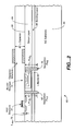
- FIG. 1A depicts a Silicon Carbide based Silicon structure of the present invention comprising a Silicon Carbide substrate, a bonding layer overlying the Silicon Carbide substrate, and a single crystal Silicon semiconductor material overlying the bonding layer and having a top surface.
- FIG. 1B shows a Silicon Carbide based Silicon structure of the present invention comprising the Silicon Carbide substrate further including a plurality of N Silicon Carbide layers, a bonding layer overlying the Silicon Carbide substrate, and a single crystal Silicon semiconductor material further including a plurality of M crystalline Silicon layers, N and M are integers.
- FIG. 2 illustrates a Silicon Carbide based Silicon structure of FIG. 1A further including at least one separation plug configured to block the coupling between at least two adjacent active/passive structures.
- FIG. 3A depicts a Silicon Carbide based Silicon structure of the present invention comprising a Silicon Carbide substrate and a single crystal Silicon semiconductor material grown on the Silicon Carbide substrate and having a top surface.
- FIG. 3B shows a Silicon Carbide based Silicon structure of the present invention comprising the Silicon Carbide substrate further including a plurality of N Silicon Carbide layers, and a single crystal Silicon semiconductor material further including a plurality of M crystalline Silicon layers, N and M are integers.
- FIG. 4A depicts a Silicon Carbide based Silicon structure of the present invention comprising: (1) a Silicon Carbide substrate; (2) a double bonding layer overlying the Silicon Carbide substrate; and (3) a single crystal Silicon semiconductor material having a top surface.
- FIG. 4B shows a Silicon Carbide based Silicon structure of FIG. 4A including a Silicon Carbide substrate further including a plurality of N Silicon Carbide layers, a single crystal Silicon semiconductor material further including a plurality of M crystalline Silicon layers, and a double bonding layer, N and M are integers.
- FIG. 1A depicts a Silicon Carbide based Silicon structure 10 comprising a Silicon Carbide substrate 12 ; a bonding layer 16 overlying the Silicon Carbide substrate 12 , and a single crystal Silicon semiconductor material 14 having a top surface 18 .
- the single crystal Silicon semiconductor material 14 is overlaying the bonding layer 16 and is bonded to the Silicon Carbide substrate 12 via the bonding layer 16 .
- the Silicon Carbide substrate 12 having a first dopant concentration (N/P) Sic I is of a conductivity type (SiC) I,II selected from the group consisting of: ⁇ a first conductivity type, and a second conductivity type ⁇ .
- the single crystal Silicon semiconductor material 14 having a second dopant concentration (N/P) Si II is of a conductivity type (Si) I,II selected from the group consisting of: ⁇ the first conductivity type, and the second conductivity type ⁇ .
- the first conductivity type is of N type, that is the majority carriers are electrons and the second conductivity is of P type, that is the majority carriers are holes.
- the first conductivity type is of P type; and the second conductivity is of N type.
- the single crystal Silicon semiconductor material is doped to be N-type by using ions of Arsenic, or ions of Phosphorous. In another embodiment, the single crystal Silicon semiconductor material is doped to be P-type by using ions of Boron. In one embodiment, the SiC substrate is doped to be N type by using ions of Nitrogen. In another embodiment, the SiC substrate is doped to be P type by using ions of Aluminum.
- the dopant concentration (N/P) SiC I/II of the Silicon Carbide substrate is equal or greater than the dopant concentration (N/P) Si I/II of the single crystal Silicon semiconductor material: ( N/P ) SiC I/II ⁇ ( N/P ) Si I/II . (1)
- the dopant concentration (N/P) SiC I/II of the Silicon Carbide substrate is less than the dopant concentration (N/P) Si I/II of the single crystal Silicon semiconductor material: ( N/P ) SiC I/II ⁇ ( N/P ) Si I/II . (2)
- the bonding layer 16 comprises a Silicon dioxide bonding layer.
- a thin layer (500 ⁇ -5000 ⁇ ) of crystalline Silicon dioxide 16 is grown by oxidizing both the SiC top surface 15 and the Silicon bottom surface 17 , or by deposition of a thin (500 ⁇ -2000 ⁇ ) layer of crystalline Silicon dioxide to the bonding surfaces 16 and 17 .
- the bonding layer 16 comprises a Silicon layer. In one more embodiment, the bonding layer 16 further comprises a carbon layer.
- the bonding layer 16 further comprises a metal silicided layer including a tungsten silicide layer, a titanium silicide layer, or a cobalt silicide layer.
- the thickness of bonding layer is typically in the range of (50-2000) ⁇ .
- the bonding layer further comprises a Silicon germanium (SiGe) layer.
- the (SiGe) layer is capable of creating a layer of “strained crystalline Silicon” that is located in close proximity to the bonding (SiGe) layer.
- Strained silicon is one of those rare new technologies that enables a fairly dramatic increase in performance with a relatively simple change in starting materials. Proof that transistors fabricated with strained silicon were faster due to increased electron mobility and velocity was first demonstrated in the mid-1980s. Then, in 1998, researchers showed it would work with leading-edge, sub-100 nm short-channel transistors. Today, companies such as Intel, IBM, Hitachi, AMD and UMC have reported success with strained silicon.
- Strained silicon stretches the distances between the silicon atoms in transistors, the tiny on/off switches that form the basis of a chip. Moving these atoms slightly farther apart reduces the atomic forces that interfere with the movement of electrons through the transistors, leading to better performance, increased carrier mobility, and lower energy consumption for the chip.
- Strained silicon works by growing a thin layer of silicon on top of a layer of silicon germanium. The atoms in the silicon layer align with those in the slightly larger crystalline lattice of the SiGe (germanium atoms are larger than silicon). This increase in spacing between the silicon atoms is enough to change how electrons are shared between the atoms, basically redefining how energy is shared in the conduction bands of the material.
- strained Silicon the atoms can be stretched (1) by inserting germanium atoms into the chip's silicon lattice, or (2) by adding a layer of silicon-germanium into the transistor bed. These two technologies are conceptually related, but different, so that they can be used in the same chip.
- the use of strained Silicon raises chip manufacturing costs by 1 or 2 percent for a performance gain of 10 percent to 20 percent.
- Si is placed on SiGe, which has a slightly wider lattice spacing than Si, then it is stretched (strained), and mobility is increased.
- a strained-Si transistor is fabricated on a Si layer deposited on a substrate containing SiGe, and uses this strained layer as the channel layer (the layer through which electrons flow).
- CMP chemical mechanical polishing
- Hitachi developed the strained-Si technology of growing the strained-Si layer on a planarized Si—Ge layer surface to achieve full performance expected in strained-Si.
- Features of the technology are as follows:
- CMP was introduced as a planarization process of the SiGe layer, and surface roughness was reduced to an atomic level flatness of 0.4 nm.
- CMP Chemical Mechanical Polishing
- the heat-treatment temperature was optimized to minimize performance degradation during the transistor fabrication process, due to diffusion of Ge from the SiGe layer to the strained-Si layer and strain relaxation of the strained-Si layer.
- MOS transistors with a channel length of 0.24 m were fabricated. Both electron and hole mobilities were found to have increased by +120% and 42% over the conventional Si transistors, respectively. The current drive was found to have significantly improved by, +70% for the ⁇ channel, and 51% for the P-channel, over the conventional Si-MOS devices. This result shows that the strained-Si technology is indeed a viable candidate for next-generation high-speed CMOS technology.
- a carbon bonding layer 16 can be formed by using the CVD process, or by performing the selective etching of the top surface 15 of the SiC substrate 12 to remove small amounts of Silicon while leaving the carbon exposed, or by combination of both processes wherein Silicon is etched from the bonding SiC surface 15 and carbon is deposited by CVD on the Silicon surface 17 to be bonded to the SiC substrate 12 .
- the Silicon bonding layer can be formed by using a Chemical Vapor Deposition (CVD) process.
- the chemical vapor deposition (CVD) process is the process in which a film is deposited by a chemical reaction or decomposition of a gas mixture at elevated temperature at the wafer surface or in its vicinity.
- the typical examples of CVD films are a single crystal Silicon film, a polycrystalline Silicon film, a crystalline Silicon dioxide film, a Silicon-nitride film, or a SiC film.
- CVD can be performed at atmospheric pressure (APCVD), or at low pressure (LPCVD).
- a lightly doped layer is deposited on a heavily doped substrate.
- the lightly doped layer is the region where active devices are constructed and the heavily doped substrate constitutes a low resistance circuit path.
- heavily doped layer is buried in a lightly doped region of opposite polarity.
- the heavily doped layer is first defined and formed in the substrate using lithography, etching, and doping techniques.
- lithography, etching, and doping techniques please, see “Fundamentals of Semiconductor Processing Technologies” by Badih El-Kareh, IBM Corporation, published by Kluwer Academic Publishers in 1995.
- the epi layer can be intentionally doped while grown by adding controlled amounts of the dopant compounds to the gas stream.
- Typical dopant sources are hybrids of the impurity, such as phosphine (PH 3 ), arsine (AsH 3 ), antimonine (SbH 3 ), or diborane (B 2 H 6 ).
- a tungsten silicide bonding layer can be deposited by using sputtering or by using the CVD process.
- a titanium silicide bonding layer, or a cobalt silicide layer can be formed by sputtering.
- Sputtering is similar to a billiard-ball event. Ions are accelerated in an electric field toward a target of material to be deposited, where they “knock-off” (sputter) target atoms. The sputtered ions then deposited onto wafers which are conveniently placed facing the target.
- Argon ion (Ark) is typically used for sputtering because it is inert and readily available in a pure form. It is ionized by colliding with high energy electrons in the chamber, and then accelerated in an electric field toward the negatively biased target. The momentum of ions incident on the target is then transferred to the surface atoms of the target material, causing ejection. Therefore, during sputter deposition, material is removed from the target and deposited onto wafers.
- FIG. 1B shows a Silicon Carbide based Silicon structure of the present invention 20 comprising the Silicon Carbide substrate 40 further including a plurality of N Silicon Carbide layers ( 22 , 24 , 26 , . . . , 28 ), a bonding layer 30 overlying the Silicon Carbide substrate 40 , and a single crystal Silicon semiconductor material 42 further including a plurality of M crystalline Silicon layers ( 38 , 36 , 34 , . . . , 32 ), N and M are integers.
- the first Silicon Carbide layer 22 includes the bottom surface of the Silicon Carbide substrate 21 .
- the last N-th Silicon Carbide layer 28 includes a top surface 29 of the Silicon Carbide substrate 40 .
- Each subsequent “k”-th layer 26 is overlying the preceding “k ⁇ 1”-th layer 24 .
- each “k”-th Silicon Carbide layer 26 includes a “k”-th conductivity type comprising the first conductivity type (SiC) I k , or the second conductivity type (SiC) II k , wherein “k” is an integer greater than one and less or equal to N.
- Each “k”-th Silicon Carbide layer includes a “k”-th dopant concentration (N/P) SiC I , or (N/P) SiC II .
- Each subsequent “k”-th Silicon Carbide layer 26 is grown on the preceding “k ⁇ 1”-th Silicon Carbide layer 24 .
- at least one Silicon Carbide layer further comprises an epitaxially grown by CVD process Silicon Carbide layer, or an epitaxially grown by a molecular beam epitaxy (MBE) process Silicon Carbide layer.
- the epi layer can be intentionally doped while grown by adding controlled amounts of the dopant compounds to the gas stream.
- the epi layer #1 of SiC 22 is grown on the bottom SiC surface 21 of the SiC substrate 40 .
- At least one Silicon Carbide layer further comprises an epitaxially grown by a molecular beam epitaxy (MBE) process Silicon Carbide layer.
- MBE molecular beam epitaxy
- MBE Molecular beam epitaxy
- MBE Molecular beam epitaxy
- High performance electronic, optoelectronic and photonic devices usually involve complex semiconductor heterostructure layers, and should be produced by advanced thin-film growth techniques such as MBE.
- MBE atoms of an element or compound are delivered to a substrate through an ultra-pure, ultra-high vacuum (UHV) atmosphere.
- UHV ultra-pure, ultra-high vacuum
- the UHV atmosphere provided by the MBE chamber allows the atoms to arrive on the substrate without colliding with other atoms or molecules. This keeps the growth free of other contaminants.
- the heated substrate surface allows the arriving atoms to distribute themselves evenly across the surface to form an almost perfect crystal structure.
- the substrate In MBE the substrate is placed in an UHV chamber with direct line of sight to several elemental species, each of which is in an evaporation furnace commonly referred to as an effusion cell.
- an effusion cell Through use of shutters and precise control of the effusion cell temperatures almost any material composition and doping can be achieved. Further, the composition may be controlled with a resolution of virtually one atomic layer.
- Applied Epi formerly EPI MBE Products Group, based in St. Paul, Minn., USA, is a leader in MBE, and manufactures the GEN 2000TM-designed to mass-produce epitaxial wafers.
- the Silicon Carbide based Silicon structure 20 further includes a plurality of M single crystal Silicon semiconductor material layers ( 38 , 36 , . . . , 34 , 32 ).
- the first single crystal Silicon semiconductor material layer 38 includes the bottom surface 31 of the single crystal Silicon semiconductor material 42 ; wherein the last M-th layer 32 includes the top surface 33 of the single crystal Silicon semiconductor material 42 .
- Each subsequent “i”-th layer 34 is overlying the preceding “i ⁇ 1”-th layer 36 .
- “i” is an integer greater than 1 and less or equal to M
- M is an integer.
- each “i”-th crystalline Silicon layer 34 includes the “i”-th conductivity type comprising the first conductivity type (Si) or the second conductivity type (Si) II i .
- Each “i”-th crystalline Silicon layer includes an “i”-th dopant concentration (N/P) Si I , or (N/P) Si II .
- At least one “i”-th single crystal Silicon semiconductor material layer further comprises an epitaxially grown by CVD process single crystal Silicon semiconductor material layer, or an epitaxially grown by MBE process single crystal Silicon semiconductor material layer. Please, see discussion above.
- the epi Si layer #1 38 is grown on the top surface 31 of the bonding layer 30 in the presence of diborane (B 2 H 6 ). This process results in a lightly Boron doped (P ⁇ ) epi crystalline Silicon layer #1 38 .
- the Silicon Carbide based Silicon structure 60 further includes at least one separation plug 62 formed in the single crystal Silicon semiconductor material 64 .
- the separation plug 62 extends from the top surface 65 of the single crystal Silicon semiconductor material 64 into the Silicon Carbide substrate 66 at a separation plug depth level L Plug (not shown).
- each separation plug is configured to block the coupling between at least two adjacent active/passive structures, wherein the first active/passive structure extends from the top surface 65 of the single crystal Silicon semiconductor material 64 into the single crystal Silicon semiconductor material 64 at a first active/passive structure depth level (not shown), and wherein the second active/passive structure L First active/passive extends from the top surface 65 of the single crystal Silicon semiconductor material 64 into the single crystal Silicon semiconductor material 64 at a second active/passive structure depth level L Second active/passive (not shown).
- the first separation plug 62 extended at the separation plug depth level L Plug1 70 separates the FET structure 72 extended at the FET structure depth level L FET 78 from the bipolar structure 74 extended at the bipolar structure depth level L Bipolar 80
- the second separation plug 76 extended at the separation plug depth level L Plug2 79 separates the bipolar structure 74 extended at the bipolar structure depth level L Bipolar 80 from the capacitor structure 78 extended at the capacitor structure depth level L Capacitor 82 .
- the separation plug depth level L Plug1 of the first plug 62 is deeper than the FET structure depth level L FET 78 and is deeper than the bipolar structure depth level L Bipolar 80 : L Plug1 >L FET ; (3) L Plug1 >L Bipolar . (4)
- the separation plug depth level L Plug2 of the second plug 76 is deeper than the bipolar structure depth level L Bipolar 80 and is deeper than the capacitor structure depth level L Capacitor 82 : L Plug2 >L Bipolar ; (5) L Plug2 >L Capacitor . (6)
- the separation plug 62 further includes a trench (not shown) filled with a material comprising: an oxide material, a polySilicon material, a metal material, a silicided material, a tungsten silicide material, a titanium silicide material, a cobalt silicide material, or a platinum silicide material.
- FIG. 3A illustrates a Silicon Carbide based Silicon structure 100 further comprising a Silicon Carbide substrate 102 , and a single crystal Silicon semiconductor material 104 having a top surface 106 .
- the single crystal Silicon semiconductor material 104 is epitaxially grown on the Silicon Carbide substrate 102 .
- the Silicon Carbide substrate 102 is of a first conductivity type (SiC) I and includes a first dopant concentration (N/P) SiC I ; wherein the single crystal Silicon semiconductor material 104 is of a second conductivity type (Si) II and has a second dopant concentration (N/P) Si II .
- the conductivity type of the Silicon Carbide (SiC) I is of P type, that is the majority carriers in the Silicon Carbide substrate are holes. In another embodiment, the conductivity type of the Silicon Carbide (SiC) I is of N type, that is the majority carriers in the Silicon Carbide substrate are electrons. In one embodiment, the conductivity type of the single crystal Silicon semiconductor material (Si) II is of P type, that is the majority carriers in the single crystal Silicon semiconductor material are holes. In one more embodiment, the conductivity type of the single crystal Silicon semiconductor material (Si) II is of N type, that is the majority carriers in the single crystal Silicon semiconductor material are electrons.
- the single crystal Silicon semiconductor material 104 can be doped to be N-type by using ions of Arsenic, or ions of Phosphorous, or can be doped to be P-type by using ions of Boron, whereas the SiC substrate 102 can be doped to be N type by using ions of Nitrogen, or can be doped to be P type by using ions of Aluminum.
- the dopant concentration (N/P) SiC I/II of the Silicon Carbide substrate is equal or greater than the dopant concentration (N/P) SiC I/II of the single crystal Silicon semiconductor material, according to Eq. (1).
- the dopant concentration (N/P) SiC I/II of the Silicon Carbide substrate is less than the dopant concentration (N/P) Si I/II of the single crystal Silicon semiconductor material, according to Eq. (2).
- FIG. 3B shows a Silicon Carbide based Silicon structure of the present invention 120 comprising the Silicon Carbide substrate 124 further including a plurality of N Silicon Carbide layers ( 126 , 128 , 130 , 132 , . . . , 134 ), and a single crystal Silicon semiconductor material 122 further including a plurality of M crystalline Silicon layers ( 142 , 144 , 146 , . . . , 148 ), N and M are integers.
- the first Silicon Carbide layer 126 includes the bottom surface of the Silicon Carbide substrate 152 .
- the last N-th Silicon Carbide layer 134 includes a top surface 136 of the Silicon Carbide substrate 124 .
- Each subsequent “k”-th layer 132 is overlying the preceding “k ⁇ 1”-th layer 130 .
- each “k”-th Silicon Carbide layer 132 includes a “k”-th conductivity type comprising the first conductivity type (SiC) I k , or the second conductivity type (SiC) II k , wherein “k” is an integer greater than one and less or equal to N.
- Each “k”-th Silicon Carbide layer includes a “k”-th dopant concentration (N/P) SiC I , or (N/P) SiC II .
- Each subsequent “k”-th Silicon Carbide layer 132 is grown on the preceding “k ⁇ 1”-th Silicon Carbide layer 130 .
- at least one Silicon Carbide layer further comprises an epitaxially grown by CVD process Silicon Carbide layer, or an epitaxially grown by a molecular beam epitaxy (MBE) process Silicon Carbide layer. (Please, see discussion above).
- the Silicon Carbide based Silicon structure 122 further includes a plurality of M single crystal Silicon semiconductor material layers ( 138 , 140 , 142 , 144 , . . . , 146 , 148 ).
- the first single crystal Silicon semiconductor material layer 138 includes the bottom surface 136 of the single crystal Silicon semiconductor material 122 ; wherein the last M-th layer 148 includes the top surface 150 of the single crystal Silicon semiconductor material 122 .
- Each subsequent “i”-th layer 144 is overlying the preceding “i ⁇ 1”-th layer 142 .
- “i” is an integer greater than 1 and less or equal to M
- M is an integer.
- each “i”-th crystalline Silicon layer 144 includes the “i”-th conductivity type comprising the first conductivity type (Si) I i , or the second conductivity type (Si) II i .
- Each “i”-th crystalline Silicon layer includes an “i”-th dopant concentration (N/P) Si I , or (N/P) Si II .
- At least one “i”-th single crystal Silicon semiconductor material layer further comprises an epitaxially grown by CVD process single crystal Silicon semiconductor material layer, or an epitaxially grown by MBE process single crystal Silicon semiconductor material layer. Please, see discussion above.
- the Silicon Carbide based Silicon structure of FIG. 3A further includes at least one separation plug (not shown) formed in the single crystal Silicon semiconductor material 104 and extending into the SiC substrate 102 .
- the complete description of this embodiment can be found from the given above description of the Silicon Carbide based Silicon structure of FIG. 1A further including at least one separation plug, as illustrated by structure 60 of FIG. 2 .
- This above given disclosure is fully applicable herein and is incorporated by reference.
- Another aspect of the present invention is directed to a Silicon Carbide based Silicon structure 200 comprising: a Silicon Carbide substrate 202 , a double bonding layer 207 overlying the Silicon Carbide substrate 202 ; and (3) a single crystal Silicon semiconductor material 208 having a top surface 209 , as depicted in FIG. 4A .
- the single crystal Silicon semiconductor material 208 is overlaying the double bonding layer 207 and is bonded to the Silicon Carbide substrate 202 via the double bonding layer 207 .
- the double bonding layer 207 further comprises: a Silicon dioxide layer 206 , and a Silicon germanium (SiGe) layer 204 .
- the Silicon Carbide substrate 202 is attached to the Silicon dioxide layer 206
- the single crystal Silicon semiconductor material 208 is attached to the Silicon germanium (SiGe) layer 204 .
- a thin layer (500 ⁇ -5000 ⁇ ) of Silicon dioxide 206 is grown by oxidizing the SiC top surface (or bonding surface) 205 , or by deposition of a thin (500 ⁇ -2000 ⁇ ) layer of Silicon dioxide to the bonding surface 205 .
- the thickness of (SiGe) layer is about 1000 ⁇ .
- the double bonding layer further comprises: a carbon layer 206 , and a Silicon germanium (SiGe) layer 204 .
- the Silicon Carbide substrate 202 is attached to the carbon layer 206
- the single crystal Silicon semiconductor material 208 is attached to the Silicon germanium (SiGe) layer 204 .
- the double bonding layer 207 further comprises: a metal silicided layer 206 , and a Silicon germanium (SiGe) layer 204 .
- the Silicon Carbide substrate 202 is attached to the metal silicided layer 206
- the single crystal Silicon semiconductor material 208 is attached to the Silicon germanium (SiGe) layer 204 .
- the metal silicided layer 206 is selected from the group consisting of: a tungsten silicide layer; a titanium silicide layer; and a cobalt silicide layer.
- FIG. 4B shows a Silicon Carbide based Silicon structure of the present invention 210 further comprising the Silicon Carbide substrate 214 further including a plurality of N Silicon Carbide layers ( 242 , 240 , . . . 238 , 236 , 234 ), a single crystal Silicon semiconductor material 224 further including a plurality of M crystalline Silicon layers ( 220 , 222 , 224 , 226 , 228 , 230 ), and the double bonding layer 248 further comprising a first boning layer 246 , and the second bonding layer 244 .
- the first Silicon Carbide layer 242 includes the bottom surface of the Silicon Carbide substrate 241 .
- the last N-th Silicon Carbide layer 234 includes a top surface 237 of the Silicon Carbide substrate 214 .
- Each subsequent “k”-th Silicon Carbide layer is overlying the preceding “k ⁇ 1”-th Silicon Carbide layer.
- the SiC substrate 214 is attached to the single crystal Silicon semiconductor material 224 via the double bonding layer 248 .
- each “k”-th Silicon Carbide layer 224 includes a “k”-th conductivity type comprising the first conductivity type (SiC) I k , or the second conductivity type (SiC) II k , wherein “k” is an integer greater than one and less or equal to N.
- Each “k”-th Silicon Carbide layer includes a “k”-th dopant concentration (N/P) SiC I , or (N/P) SiC II .
- At least one Silicon Carbide layer further comprises an epitaxially grown by CVD process Silicon Carbide layer, or an epitaxially grown by a molecular beam epitaxy (MBE) process Silicon Carbide layer. (Please, see discussion above).
- MBE molecular beam epitaxy
- the Silicon Carbide based Silicon structure 210 further includes a plurality of M single crystal Silicon semiconductor material layers ( 222 , 224 , 226 , 228 , . . . 230 ).
- the first single crystal Silicon semiconductor material layer 230 is attached to the second bonding layer 244 .
- Each subsequent “i”-th layer is overlying the preceding “i ⁇ 1”-th layer.
- i is an integer greater than 1 and less or equal to M
- M is an integer.
- each “i”-th crystalline Silicon layer includes the “i”-th conductivity type comprising the first conductivity type (Si) I i , or the second conductivity type (Si) II i .
- Each “i”-th crystalline Silicon layer includes an “i”-th dopant concentration (N/P) Si I , or (N/P) Si II .
Abstract
Description
(N/P)SiC I/II≧(N/P)Si I/II. (1)
(N/P)SiC I/II<(N/P)Si I/II. (2)
L Plug1 >L FET; (3)
L Plug1 >L Bipolar. (4)
L Plug2 >L Bipolar; (5)
L Plug2 >L Capacitor. (6)
Claims (20)
Priority Applications (1)
| Application Number | Priority Date | Filing Date | Title |
|---|---|---|---|
| US10/656,613 US8080826B1 (en) | 2002-02-14 | 2003-09-04 | High performance active and passive structures based on silicon material bonded to silicon carbide |
Applications Claiming Priority (2)
| Application Number | Priority Date | Filing Date | Title |
|---|---|---|---|
| US10/078,588 US20030151051A1 (en) | 2002-02-14 | 2002-02-14 | High performance active and passive structures based on silicon material grown epitaxially or bonded to silicon carbide substrate |
| US10/656,613 US8080826B1 (en) | 2002-02-14 | 2003-09-04 | High performance active and passive structures based on silicon material bonded to silicon carbide |
Related Parent Applications (1)
| Application Number | Title | Priority Date | Filing Date |
|---|---|---|---|
| US10/078,588 Continuation-In-Part US20030151051A1 (en) | 2002-02-14 | 2002-02-14 | High performance active and passive structures based on silicon material grown epitaxially or bonded to silicon carbide substrate |
Publications (1)
| Publication Number | Publication Date |
|---|---|
| US8080826B1 true US8080826B1 (en) | 2011-12-20 |
Family
ID=45219203
Family Applications (1)
| Application Number | Title | Priority Date | Filing Date |
|---|---|---|---|
| US10/656,613 Expired - Fee Related US8080826B1 (en) | 2002-02-14 | 2003-09-04 | High performance active and passive structures based on silicon material bonded to silicon carbide |
Country Status (1)
| Country | Link |
|---|---|
| US (1) | US8080826B1 (en) |
Cited By (6)
| Publication number | Priority date | Publication date | Assignee | Title |
|---|---|---|---|---|
| US20110079793A1 (en) * | 2009-10-02 | 2011-04-07 | Seiko Epson Corporation | Semiconductor substrate and its manufacturing method |
| US20110101374A1 (en) * | 2009-10-30 | 2011-05-05 | Sei-Hyung Ryu | Monolithic high voltage switching devices and related methods of fabricating the same |
| US20120056201A1 (en) * | 2009-05-11 | 2012-03-08 | Sumitomo Electric Industries, Ltd. | Insulated gate bipolar transistor |
| US20150041824A1 (en) * | 2013-08-07 | 2015-02-12 | International Business Machines Corporation | Transistor with bonded gate dielectric |
| US20180171471A1 (en) * | 2016-12-21 | 2018-06-21 | Nuflare Technology, Inc. | Vapor phase growth method |
| US10204793B2 (en) * | 2016-05-17 | 2019-02-12 | Taiwan Semiconductor Manufacturing Company Ltd. | Chemical mechanical polishing slurry, method for chemical mechanical polishing and manufacturing method of semiconductor structure |
Citations (9)
| Publication number | Priority date | Publication date | Assignee | Title |
|---|---|---|---|---|
| US5296047A (en) * | 1992-01-28 | 1994-03-22 | Hewlett-Packard Co. | Epitaxial silicon starting material |
| US5349207A (en) * | 1993-02-22 | 1994-09-20 | Texas Instruments Incorporated | Silicon carbide wafer bonded to a silicon wafer |
| US5488232A (en) | 1993-09-28 | 1996-01-30 | North Carolina State University | Oriented diamond film structures on non-diamond substrates |
| US6117751A (en) | 1996-07-19 | 2000-09-12 | Siemens Aktiengesellschaft | Method for manufacturing a mis structure on silicon carbide (SiC) |
| JP2001036069A (en) * | 1999-07-21 | 2001-02-09 | Toyota Central Res & Dev Lab Inc | Diode |
| US6211041B1 (en) * | 1998-04-17 | 2001-04-03 | Nec Corporation | Silicon-on-insulator (SOI) substrate and method of fabricating the same |
| US6426968B1 (en) | 1982-05-04 | 2002-07-30 | United Technologies Corporation | Hybrid optical mirror |
| US6521923B1 (en) * | 2002-05-25 | 2003-02-18 | Sirenza Microdevices, Inc. | Microwave field effect transistor structure on silicon carbide substrate |
| US20030094672A1 (en) * | 2001-11-21 | 2003-05-22 | Torvik John Tarje | Heterojunction bipolar transistor containing at least one silicon carbide layer |
-
2003
- 2003-09-04 US US10/656,613 patent/US8080826B1/en not_active Expired - Fee Related
Patent Citations (9)
| Publication number | Priority date | Publication date | Assignee | Title |
|---|---|---|---|---|
| US6426968B1 (en) | 1982-05-04 | 2002-07-30 | United Technologies Corporation | Hybrid optical mirror |
| US5296047A (en) * | 1992-01-28 | 1994-03-22 | Hewlett-Packard Co. | Epitaxial silicon starting material |
| US5349207A (en) * | 1993-02-22 | 1994-09-20 | Texas Instruments Incorporated | Silicon carbide wafer bonded to a silicon wafer |
| US5488232A (en) | 1993-09-28 | 1996-01-30 | North Carolina State University | Oriented diamond film structures on non-diamond substrates |
| US6117751A (en) | 1996-07-19 | 2000-09-12 | Siemens Aktiengesellschaft | Method for manufacturing a mis structure on silicon carbide (SiC) |
| US6211041B1 (en) * | 1998-04-17 | 2001-04-03 | Nec Corporation | Silicon-on-insulator (SOI) substrate and method of fabricating the same |
| JP2001036069A (en) * | 1999-07-21 | 2001-02-09 | Toyota Central Res & Dev Lab Inc | Diode |
| US20030094672A1 (en) * | 2001-11-21 | 2003-05-22 | Torvik John Tarje | Heterojunction bipolar transistor containing at least one silicon carbide layer |
| US6521923B1 (en) * | 2002-05-25 | 2003-02-18 | Sirenza Microdevices, Inc. | Microwave field effect transistor structure on silicon carbide substrate |
Non-Patent Citations (3)
| Title |
|---|
| Hiroyuki Nagasawa, Kuniaki Yogi, Takamitsu Kawahara and Naki Hatta; "3C-SiC Monocrystals Grown on Undulant Si(001) Substrates" pp. 47 & 50; Material Research Society vol. 742 ® 2003. |
| Wolf, Silicon Processing for the VLSI Era: vol. 1-Process Technology, Lattice Press, 2000, 2nd edition, p. 226. * |
| Zhiyun Cheng et al.; Relaxed Silicon-Germanium On Insulator (SG01); Material Research Society Symp. Proc. vol. 686; 2002 p. 21-26. |
Cited By (10)
| Publication number | Priority date | Publication date | Assignee | Title |
|---|---|---|---|---|
| US20120056201A1 (en) * | 2009-05-11 | 2012-03-08 | Sumitomo Electric Industries, Ltd. | Insulated gate bipolar transistor |
| US20110079793A1 (en) * | 2009-10-02 | 2011-04-07 | Seiko Epson Corporation | Semiconductor substrate and its manufacturing method |
| US8431935B2 (en) * | 2009-10-02 | 2013-04-30 | Seiko Epson Corporation | Semiconductor substrate with cobalt silicide buffer layer and its manufacturing method |
| US20110101374A1 (en) * | 2009-10-30 | 2011-05-05 | Sei-Hyung Ryu | Monolithic high voltage switching devices and related methods of fabricating the same |
| US8610130B2 (en) * | 2009-10-30 | 2013-12-17 | Cree, Inc. | Monolithic high voltage switching devices |
| US20150041824A1 (en) * | 2013-08-07 | 2015-02-12 | International Business Machines Corporation | Transistor with bonded gate dielectric |
| US9373691B2 (en) * | 2013-08-07 | 2016-06-21 | GlobalFoundries, Inc. | Transistor with bonded gate dielectric |
| US10204793B2 (en) * | 2016-05-17 | 2019-02-12 | Taiwan Semiconductor Manufacturing Company Ltd. | Chemical mechanical polishing slurry, method for chemical mechanical polishing and manufacturing method of semiconductor structure |
| US20180171471A1 (en) * | 2016-12-21 | 2018-06-21 | Nuflare Technology, Inc. | Vapor phase growth method |
| US10351949B2 (en) * | 2016-12-21 | 2019-07-16 | Nuflare Technology, Inc. | Vapor phase growth method |
Similar Documents
| Publication | Publication Date | Title |
|---|---|---|
| JP5141029B2 (en) | Semiconductor device and manufacturing method thereof | |
| US6852602B2 (en) | Semiconductor crystal film and method for preparation thereof | |
| US7023018B2 (en) | SiGe transistor with strained layers | |
| US7164183B2 (en) | Semiconductor substrate, semiconductor device, and method of manufacturing the same | |
| US10170302B2 (en) | Superlattice lateral bipolar junction transistor | |
| US9112029B2 (en) | Strained transistor integration for CMOS | |
| US6936869B2 (en) | Heterojunction field effect transistors using silicon-germanium and silicon-carbon alloys | |
| EP1697994B1 (en) | Transistor gate electrode having conductor material layer and method of fabrication | |
| US7829442B2 (en) | Semiconductor heterostructures having reduced dislocation pile-ups and related methods | |
| US8105908B2 (en) | Methods for forming a transistor and modulating channel stress | |
| US20070029553A1 (en) | Methods of fabricating strained semiconductor-on-insulator field-effect transistors and related devices | |
| JP2007521648A (en) | Semiconductor device having MOSFET with band design superlattice | |
| JP2007521646A (en) | Semiconductor device having a band design superlattice | |
| CN1574252A (en) | Method for preparing lateral channel of field effect transistor, and field effect transistor | |
| US20110042728A1 (en) | Semiconductor device with enhanced stress by gates stress liner | |
| US20060211221A1 (en) | Method for producing a strained layer on a substrate and corresponding layer structure | |
| Jun et al. | Electrical characteristics of thin-film transistors using field-aided lateral crystallization | |
| Brunco et al. | Germanium: The past and possibly a future material for microelectronics | |
| JP2005510081A (en) | Fabrication method of high mobility silicon germanium structure by low energy plasma enhanced chemical vapor deposition | |
| US8080826B1 (en) | High performance active and passive structures based on silicon material bonded to silicon carbide | |
| US20030151051A1 (en) | High performance active and passive structures based on silicon material grown epitaxially or bonded to silicon carbide substrate | |
| CA1170787A (en) | Semiconductor device | |
| JP3708881B2 (en) | Semiconductor crystal film, manufacturing method thereof, semiconductor device and manufacturing method thereof | |
| US10332979B2 (en) | Methods and systems for reducing dislocation defects in high concentration epitaxy processes | |
| Wang et al. | Optimized Si-Cap Layer Thickness for Tensile-Strained-Si/Compressively Strained SiGe Dual-Channel Transistors in 0.13 µm Complementary Metal Oxide Semiconductor Technology |
Legal Events
| Date | Code | Title | Description |
|---|---|---|---|
| AS | Assignment |
Owner name: SIRENZA MICRODEVICES, INC., COLORADO Free format text: ASSIGNMENT OF ASSIGNORS INTEREST;ASSIGNORS:JOHNSON, JOSEPH H.;D'ANNA, PABLO E.;REEL/FRAME:014481/0207 Effective date: 20030829 |
|
| AS | Assignment |
Owner name: RF MICRO DEVICES, INC., NORTH CAROLINA Free format text: ASSIGNMENT OF ASSIGNORS INTEREST;ASSIGNOR:SIRENZA MICRODEVICES;REEL/FRAME:020927/0797 Effective date: 20080505 |
|
| ZAAA | Notice of allowance and fees due |
Free format text: ORIGINAL CODE: NOA |
|
| ZAAB | Notice of allowance mailed |
Free format text: ORIGINAL CODE: MN/=. |
|
| STCF | Information on status: patent grant |
Free format text: PATENTED CASE |
|
| AS | Assignment |
Owner name: BANK OF AMERICA, N.A., AS ADMINISTRATIVE AGENT, TE Free format text: NOTICE OF GRANT OF SECURITY INTEREST IN PATENTS;ASSIGNOR:RF MICRO DEVICES, INC.;REEL/FRAME:030045/0831 Effective date: 20130319 |
|
| AS | Assignment |
Owner name: RF MICRO DEVICES, INC., NORTH CAROLINA Free format text: CORRECTIVE ASSIGNMENT TO CORRECT THE NAME OF THE ASSIGNOR TO READ SIRENZA MICRODEVICES, INC. PREVIOUSLY RECORDED ON REEL 020927 FRAME 0797. ASSIGNOR(S) HEREBY CONFIRMS THE NAME OF THE ASSIGNEE IS RF MICRO DEVICES, INC.;ASSIGNOR:SIRENZA MICRODEVICES, INC.;REEL/FRAME:030677/0162 Effective date: 20080505 |
|
| AS | Assignment |
Owner name: RF MICRO DEVICES, INC., NORTH CAROLINA Free format text: TERMINATION AND RELEASE OF SECURITY INTEREST IN PATENTS (RECORDED 3/19/13 AT REEL/FRAME 030045/0831);ASSIGNOR:BANK OF AMERICA, N.A., AS ADMINISTRATIVE AGENT;REEL/FRAME:035334/0363 Effective date: 20150326 |
|
| FPAY | Fee payment |
Year of fee payment: 4 |
|
| AS | Assignment |
Owner name: QORVO US, INC., NORTH CAROLINA Free format text: MERGER;ASSIGNOR:RF MICRO DEVICES, INC.;REEL/FRAME:039196/0941 Effective date: 20160330 |
|
| FEPP | Fee payment procedure |
Free format text: MAINTENANCE FEE REMINDER MAILED (ORIGINAL EVENT CODE: REM.); ENTITY STATUS OF PATENT OWNER: LARGE ENTITY |
|
| FEPP | Fee payment procedure |
Free format text: 7.5 YR SURCHARGE - LATE PMT W/IN 6 MO, LARGE ENTITY (ORIGINAL EVENT CODE: M1555); ENTITY STATUS OF PATENT OWNER: LARGE ENTITY |
|
| MAFP | Maintenance fee payment |
Free format text: PAYMENT OF MAINTENANCE FEE, 8TH YEAR, LARGE ENTITY (ORIGINAL EVENT CODE: M1552); ENTITY STATUS OF PATENT OWNER: LARGE ENTITY Year of fee payment: 8 |
|
| FEPP | Fee payment procedure |
Free format text: MAINTENANCE FEE REMINDER MAILED (ORIGINAL EVENT CODE: REM.); ENTITY STATUS OF PATENT OWNER: LARGE ENTITY |
|
| LAPS | Lapse for failure to pay maintenance fees |
Free format text: PATENT EXPIRED FOR FAILURE TO PAY MAINTENANCE FEES (ORIGINAL EVENT CODE: EXP.); ENTITY STATUS OF PATENT OWNER: LARGE ENTITY |
|
| STCH | Information on status: patent discontinuation |
Free format text: PATENT EXPIRED DUE TO NONPAYMENT OF MAINTENANCE FEES UNDER 37 CFR 1.362 |
|
| FP | Lapsed due to failure to pay maintenance fee |
Effective date: 20231220 |