US8076696B2 - Power module assembly with reduced inductance - Google Patents
Power module assembly with reduced inductance Download PDFInfo
- Publication number
- US8076696B2 US8076696B2 US12/609,400 US60940009A US8076696B2 US 8076696 B2 US8076696 B2 US 8076696B2 US 60940009 A US60940009 A US 60940009A US 8076696 B2 US8076696 B2 US 8076696B2
- Authority
- US
- United States
- Prior art keywords
- positive
- power semiconductor
- negative
- output
- terminal
- Prior art date
- Legal status (The legal status is an assumption and is not a legal conclusion. Google has not performed a legal analysis and makes no representation as to the accuracy of the status listed.)
- Active
Links
Images


Classifications
-
- H—ELECTRICITY
- H01—ELECTRIC ELEMENTS
- H01L—SEMICONDUCTOR DEVICES NOT COVERED BY CLASS H10
- H01L24/00—Arrangements for connecting or disconnecting semiconductor or solid-state bodies; Methods or apparatus related thereto
- H01L24/01—Means for bonding being attached to, or being formed on, the surface to be connected, e.g. chip-to-package, die-attach, "first-level" interconnects; Manufacturing methods related thereto
- H01L24/42—Wire connectors; Manufacturing methods related thereto
- H01L24/47—Structure, shape, material or disposition of the wire connectors after the connecting process
- H01L24/49—Structure, shape, material or disposition of the wire connectors after the connecting process of a plurality of wire connectors
-
- H—ELECTRICITY
- H01—ELECTRIC ELEMENTS
- H01L—SEMICONDUCTOR DEVICES NOT COVERED BY CLASS H10
- H01L25/00—Assemblies consisting of a plurality of individual semiconductor or other solid state devices ; Multistep manufacturing processes thereof
- H01L25/03—Assemblies consisting of a plurality of individual semiconductor or other solid state devices ; Multistep manufacturing processes thereof all the devices being of a type provided for in the same subgroup of groups H01L27/00 - H01L33/00, or in a single subclass of H10K, H10N, e.g. assemblies of rectifier diodes
- H01L25/04—Assemblies consisting of a plurality of individual semiconductor or other solid state devices ; Multistep manufacturing processes thereof all the devices being of a type provided for in the same subgroup of groups H01L27/00 - H01L33/00, or in a single subclass of H10K, H10N, e.g. assemblies of rectifier diodes the devices not having separate containers
- H01L25/07—Assemblies consisting of a plurality of individual semiconductor or other solid state devices ; Multistep manufacturing processes thereof all the devices being of a type provided for in the same subgroup of groups H01L27/00 - H01L33/00, or in a single subclass of H10K, H10N, e.g. assemblies of rectifier diodes the devices not having separate containers the devices being of a type provided for in group H01L29/00
- H01L25/072—Assemblies consisting of a plurality of individual semiconductor or other solid state devices ; Multistep manufacturing processes thereof all the devices being of a type provided for in the same subgroup of groups H01L27/00 - H01L33/00, or in a single subclass of H10K, H10N, e.g. assemblies of rectifier diodes the devices not having separate containers the devices being of a type provided for in group H01L29/00 the devices being arranged next to each other
-
- H—ELECTRICITY
- H01—ELECTRIC ELEMENTS
- H01L—SEMICONDUCTOR DEVICES NOT COVERED BY CLASS H10
- H01L2224/00—Indexing scheme for arrangements for connecting or disconnecting semiconductor or solid-state bodies and methods related thereto as covered by H01L24/00
- H01L2224/01—Means for bonding being attached to, or being formed on, the surface to be connected, e.g. chip-to-package, die-attach, "first-level" interconnects; Manufacturing methods related thereto
- H01L2224/42—Wire connectors; Manufacturing methods related thereto
- H01L2224/47—Structure, shape, material or disposition of the wire connectors after the connecting process
- H01L2224/48—Structure, shape, material or disposition of the wire connectors after the connecting process of an individual wire connector
- H01L2224/4805—Shape
- H01L2224/4809—Loop shape
- H01L2224/48091—Arched
-
- H—ELECTRICITY
- H01—ELECTRIC ELEMENTS
- H01L—SEMICONDUCTOR DEVICES NOT COVERED BY CLASS H10
- H01L2224/00—Indexing scheme for arrangements for connecting or disconnecting semiconductor or solid-state bodies and methods related thereto as covered by H01L24/00
- H01L2224/01—Means for bonding being attached to, or being formed on, the surface to be connected, e.g. chip-to-package, die-attach, "first-level" interconnects; Manufacturing methods related thereto
- H01L2224/42—Wire connectors; Manufacturing methods related thereto
- H01L2224/47—Structure, shape, material or disposition of the wire connectors after the connecting process
- H01L2224/48—Structure, shape, material or disposition of the wire connectors after the connecting process of an individual wire connector
- H01L2224/481—Disposition
- H01L2224/48135—Connecting between different semiconductor or solid-state bodies, i.e. chip-to-chip
- H01L2224/48137—Connecting between different semiconductor or solid-state bodies, i.e. chip-to-chip the bodies being arranged next to each other, e.g. on a common substrate
-
- H—ELECTRICITY
- H01—ELECTRIC ELEMENTS
- H01L—SEMICONDUCTOR DEVICES NOT COVERED BY CLASS H10
- H01L2224/00—Indexing scheme for arrangements for connecting or disconnecting semiconductor or solid-state bodies and methods related thereto as covered by H01L24/00
- H01L2224/01—Means for bonding being attached to, or being formed on, the surface to be connected, e.g. chip-to-package, die-attach, "first-level" interconnects; Manufacturing methods related thereto
- H01L2224/42—Wire connectors; Manufacturing methods related thereto
- H01L2224/47—Structure, shape, material or disposition of the wire connectors after the connecting process
- H01L2224/48—Structure, shape, material or disposition of the wire connectors after the connecting process of an individual wire connector
- H01L2224/484—Connecting portions
- H01L2224/4847—Connecting portions the connecting portion on the bonding area of the semiconductor or solid-state body being a wedge bond
- H01L2224/48472—Connecting portions the connecting portion on the bonding area of the semiconductor or solid-state body being a wedge bond the other connecting portion not on the bonding area also being a wedge bond, i.e. wedge-to-wedge
-
- H—ELECTRICITY
- H01—ELECTRIC ELEMENTS
- H01L—SEMICONDUCTOR DEVICES NOT COVERED BY CLASS H10
- H01L2224/00—Indexing scheme for arrangements for connecting or disconnecting semiconductor or solid-state bodies and methods related thereto as covered by H01L24/00
- H01L2224/01—Means for bonding being attached to, or being formed on, the surface to be connected, e.g. chip-to-package, die-attach, "first-level" interconnects; Manufacturing methods related thereto
- H01L2224/42—Wire connectors; Manufacturing methods related thereto
- H01L2224/47—Structure, shape, material or disposition of the wire connectors after the connecting process
- H01L2224/49—Structure, shape, material or disposition of the wire connectors after the connecting process of a plurality of wire connectors
- H01L2224/491—Disposition
- H01L2224/4911—Disposition the connectors being bonded to at least one common bonding area, e.g. daisy chain
-
- H—ELECTRICITY
- H01—ELECTRIC ELEMENTS
- H01L—SEMICONDUCTOR DEVICES NOT COVERED BY CLASS H10
- H01L2224/00—Indexing scheme for arrangements for connecting or disconnecting semiconductor or solid-state bodies and methods related thereto as covered by H01L24/00
- H01L2224/73—Means for bonding being of different types provided for in two or more of groups H01L2224/10, H01L2224/18, H01L2224/26, H01L2224/34, H01L2224/42, H01L2224/50, H01L2224/63, H01L2224/71
- H01L2224/732—Location after the connecting process
- H01L2224/73251—Location after the connecting process on different surfaces
- H01L2224/73265—Layer and wire connectors
-
- H—ELECTRICITY
- H01—ELECTRIC ELEMENTS
- H01L—SEMICONDUCTOR DEVICES NOT COVERED BY CLASS H10
- H01L24/00—Arrangements for connecting or disconnecting semiconductor or solid-state bodies; Methods or apparatus related thereto
- H01L24/01—Means for bonding being attached to, or being formed on, the surface to be connected, e.g. chip-to-package, die-attach, "first-level" interconnects; Manufacturing methods related thereto
- H01L24/42—Wire connectors; Manufacturing methods related thereto
- H01L24/47—Structure, shape, material or disposition of the wire connectors after the connecting process
- H01L24/48—Structure, shape, material or disposition of the wire connectors after the connecting process of an individual wire connector
-
- H—ELECTRICITY
- H01—ELECTRIC ELEMENTS
- H01L—SEMICONDUCTOR DEVICES NOT COVERED BY CLASS H10
- H01L2924/00—Indexing scheme for arrangements or methods for connecting or disconnecting semiconductor or solid-state bodies as covered by H01L24/00
- H01L2924/0001—Technical content checked by a classifier
- H01L2924/00014—Technical content checked by a classifier the subject-matter covered by the group, the symbol of which is combined with the symbol of this group, being disclosed without further technical details
-
- H—ELECTRICITY
- H01—ELECTRIC ELEMENTS
- H01L—SEMICONDUCTOR DEVICES NOT COVERED BY CLASS H10
- H01L2924/00—Indexing scheme for arrangements or methods for connecting or disconnecting semiconductor or solid-state bodies as covered by H01L24/00
- H01L2924/01—Chemical elements
- H01L2924/01004—Beryllium [Be]
-
- H—ELECTRICITY
- H01—ELECTRIC ELEMENTS
- H01L—SEMICONDUCTOR DEVICES NOT COVERED BY CLASS H10
- H01L2924/00—Indexing scheme for arrangements or methods for connecting or disconnecting semiconductor or solid-state bodies as covered by H01L24/00
- H01L2924/01—Chemical elements
- H01L2924/01006—Carbon [C]
-
- H—ELECTRICITY
- H01—ELECTRIC ELEMENTS
- H01L—SEMICONDUCTOR DEVICES NOT COVERED BY CLASS H10
- H01L2924/00—Indexing scheme for arrangements or methods for connecting or disconnecting semiconductor or solid-state bodies as covered by H01L24/00
- H01L2924/01—Chemical elements
- H01L2924/01014—Silicon [Si]
-
- H—ELECTRICITY
- H01—ELECTRIC ELEMENTS
- H01L—SEMICONDUCTOR DEVICES NOT COVERED BY CLASS H10
- H01L2924/00—Indexing scheme for arrangements or methods for connecting or disconnecting semiconductor or solid-state bodies as covered by H01L24/00
- H01L2924/01—Chemical elements
- H01L2924/01023—Vanadium [V]
-
- H—ELECTRICITY
- H01—ELECTRIC ELEMENTS
- H01L—SEMICONDUCTOR DEVICES NOT COVERED BY CLASS H10
- H01L2924/00—Indexing scheme for arrangements or methods for connecting or disconnecting semiconductor or solid-state bodies as covered by H01L24/00
- H01L2924/01—Chemical elements
- H01L2924/01029—Copper [Cu]
-
- H—ELECTRICITY
- H01—ELECTRIC ELEMENTS
- H01L—SEMICONDUCTOR DEVICES NOT COVERED BY CLASS H10
- H01L2924/00—Indexing scheme for arrangements or methods for connecting or disconnecting semiconductor or solid-state bodies as covered by H01L24/00
- H01L2924/01—Chemical elements
- H01L2924/01033—Arsenic [As]
-
- H—ELECTRICITY
- H01—ELECTRIC ELEMENTS
- H01L—SEMICONDUCTOR DEVICES NOT COVERED BY CLASS H10
- H01L2924/00—Indexing scheme for arrangements or methods for connecting or disconnecting semiconductor or solid-state bodies as covered by H01L24/00
- H01L2924/01—Chemical elements
- H01L2924/01074—Tungsten [W]
-
- H—ELECTRICITY
- H01—ELECTRIC ELEMENTS
- H01L—SEMICONDUCTOR DEVICES NOT COVERED BY CLASS H10
- H01L2924/00—Indexing scheme for arrangements or methods for connecting or disconnecting semiconductor or solid-state bodies as covered by H01L24/00
- H01L2924/01—Chemical elements
- H01L2924/01082—Lead [Pb]
-
- H—ELECTRICITY
- H01—ELECTRIC ELEMENTS
- H01L—SEMICONDUCTOR DEVICES NOT COVERED BY CLASS H10
- H01L2924/00—Indexing scheme for arrangements or methods for connecting or disconnecting semiconductor or solid-state bodies as covered by H01L24/00
- H01L2924/013—Alloys
- H01L2924/014—Solder alloys
-
- H—ELECTRICITY
- H01—ELECTRIC ELEMENTS
- H01L—SEMICONDUCTOR DEVICES NOT COVERED BY CLASS H10
- H01L2924/00—Indexing scheme for arrangements or methods for connecting or disconnecting semiconductor or solid-state bodies as covered by H01L24/00
- H01L2924/10—Details of semiconductor or other solid state devices to be connected
- H01L2924/11—Device type
- H01L2924/12—Passive devices, e.g. 2 terminal devices
- H01L2924/1203—Rectifying Diode
- H01L2924/12032—Schottky diode
-
- H—ELECTRICITY
- H01—ELECTRIC ELEMENTS
- H01L—SEMICONDUCTOR DEVICES NOT COVERED BY CLASS H10
- H01L2924/00—Indexing scheme for arrangements or methods for connecting or disconnecting semiconductor or solid-state bodies as covered by H01L24/00
- H01L2924/10—Details of semiconductor or other solid state devices to be connected
- H01L2924/11—Device type
- H01L2924/13—Discrete devices, e.g. 3 terminal devices
- H01L2924/1301—Thyristor
-
- H—ELECTRICITY
- H01—ELECTRIC ELEMENTS
- H01L—SEMICONDUCTOR DEVICES NOT COVERED BY CLASS H10
- H01L2924/00—Indexing scheme for arrangements or methods for connecting or disconnecting semiconductor or solid-state bodies as covered by H01L24/00
- H01L2924/10—Details of semiconductor or other solid state devices to be connected
- H01L2924/11—Device type
- H01L2924/13—Discrete devices, e.g. 3 terminal devices
- H01L2924/1304—Transistor
- H01L2924/1305—Bipolar Junction Transistor [BJT]
- H01L2924/13055—Insulated gate bipolar transistor [IGBT]
-
- H—ELECTRICITY
- H01—ELECTRIC ELEMENTS
- H01L—SEMICONDUCTOR DEVICES NOT COVERED BY CLASS H10
- H01L2924/00—Indexing scheme for arrangements or methods for connecting or disconnecting semiconductor or solid-state bodies as covered by H01L24/00
- H01L2924/10—Details of semiconductor or other solid state devices to be connected
- H01L2924/11—Device type
- H01L2924/13—Discrete devices, e.g. 3 terminal devices
- H01L2924/1304—Transistor
- H01L2924/1306—Field-effect transistor [FET]
- H01L2924/13091—Metal-Oxide-Semiconductor Field-Effect Transistor [MOSFET]
-
- H—ELECTRICITY
- H01—ELECTRIC ELEMENTS
- H01L—SEMICONDUCTOR DEVICES NOT COVERED BY CLASS H10
- H01L2924/00—Indexing scheme for arrangements or methods for connecting or disconnecting semiconductor or solid-state bodies as covered by H01L24/00
- H01L2924/15—Details of package parts other than the semiconductor or other solid state devices to be connected
- H01L2924/151—Die mounting substrate
- H01L2924/156—Material
- H01L2924/157—Material with a principal constituent of the material being a metal or a metalloid, e.g. boron [B], silicon [Si], germanium [Ge], arsenic [As], antimony [Sb], tellurium [Te] and polonium [Po], and alloys thereof
- H01L2924/15738—Material with a principal constituent of the material being a metal or a metalloid, e.g. boron [B], silicon [Si], germanium [Ge], arsenic [As], antimony [Sb], tellurium [Te] and polonium [Po], and alloys thereof the principal constituent melting at a temperature of greater than or equal to 950 C and less than 1550 C
- H01L2924/15747—Copper [Cu] as principal constituent
-
- H—ELECTRICITY
- H01—ELECTRIC ELEMENTS
- H01L—SEMICONDUCTOR DEVICES NOT COVERED BY CLASS H10
- H01L2924/00—Indexing scheme for arrangements or methods for connecting or disconnecting semiconductor or solid-state bodies as covered by H01L24/00
- H01L2924/19—Details of hybrid assemblies other than the semiconductor or other solid state devices to be connected
- H01L2924/191—Disposition
- H01L2924/19101—Disposition of discrete passive components
- H01L2924/19107—Disposition of discrete passive components off-chip wires
-
- H—ELECTRICITY
- H01—ELECTRIC ELEMENTS
- H01L—SEMICONDUCTOR DEVICES NOT COVERED BY CLASS H10
- H01L2924/00—Indexing scheme for arrangements or methods for connecting or disconnecting semiconductor or solid-state bodies as covered by H01L24/00
- H01L2924/30—Technical effects
- H01L2924/301—Electrical effects
- H01L2924/30107—Inductance
Definitions
- Embodiments of the invention relate generally to power modules, and more particularly to power modules having reduced parasitic inductance.
- parasitic inductance can lead to increased power losses resulting from greater voltage and current oscillation and reduced reliability due to greater overvoltage stresses applied to the power semiconductors (IGBTs, MOSFETs, diodes, etc.). Therefore, it may be desirable in some cases to minimize parasitic inductance of the power module.
- a device such as a power module
- the device can include a first conductive substrate and a second conductive substrate.
- a first power semiconductor component having a first thickness can be electrically coupled to (and possibly disposed on) the first conductive substrate.
- a second power semiconductor component having a second thickness can be electrically coupled to (and possible disposed on) the second conductive substrate.
- the first and second power semiconductor components can include opposing front and back surfaces, and the back surface of the first power semiconductor component can be electrically coupled to the first conductive substrate and the back surface of the second power semiconductor component being electrically coupled to the second conductive substrate.
- a positive terminal can also be electrically coupled to the first conductive substrate, while a negative terminal can be electrically coupled to the second power semiconductor component, and an output terminal may be electrically coupled to the first power semiconductor component and the second conductive substrate.
- the positive, negative, and output terminals may, for example, be configured to support an instantaneous electrical current of at least about 10 A.
- the negative terminal may substantially oppose the positive terminal, for example, as where the positive and negative terminals abut opposing sides of a power insulation layer.
- the positive and negative terminals can be substantially planar.
- the output terminal and the positive terminal abut opposing sides of an output insulation layer, and the output terminal and the negative terminal may also abut opposing sides of the output insulation layer.
- the device may also include a substantially planar baseplate.
- the first and second conductive substrates can be respectively disposed on the baseplate and the positive and negative terminals may extend substantially perpendicularly away from the baseplate.
- a respective diode connected in an anti-parallel arrangement across each of the first and second power semiconductor components may also be included.
- the device may further include a connector configured to electrically couple the positive and negative terminals to respective busbars.
- the connector may include opposing electrodes configured to make respective electrical contact with the positive and negative terminals.
- a separation distance between the opposing electrodes can be substantially similar to an aggregate thickness of the positive and negative terminals and a power insulation layer disposed therebetween.
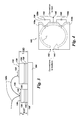
- FIG. 1 is a perspective view of a power module configured in accordance with an example embodiment
- FIG. 2 is a side view of the power module of FIG. 1 ;
- FIG. 3 is a magnified side view of the region labeled 3 in FIG. 2 ;
- FIG. 4 is a schematic view of the power module of FIG. 1 , showing the circuit formed by the components thereof;
- FIG. 6 is a side view of the power module of FIG. 1 illustrating the area defined by the path along which current flows when the switch structures of the module are in a conducting state;
- FIG. 7 is a plan view of the power module of FIG. 1 ;
- FIG. 8 is a perspective view of the power module of FIG. 1 and an associated connector
- FIG. 10 is a perspective view of the coupled power module and connector of FIG. 9 ;
- FIG. 11 is a side view of the coupled power module and connector of FIG. 9 ;
- FIG. 12 is a cross sectional view of the coupled power module and connector of FIG. 9 ;
- FIG. 13 is a perspective view of a power module configured in accordance with another example embodiment
- FIG. 14 is a cross sectional view of the power module of FIG. 13 ;
- FIG. 15 is a perspective view of a power module configured in accordance with yet another example embodiment.
- the power module 100 can include a first and a second conductive substrate 102 , 104 .
- each of the first and second conductive substrates 102 , 104 may include a respective patterned copper layer, which layers can be disposed on respective ceramic tiles 106 , 108 so as to form parts of respective power electronic substrates, such as a direct bonded copper substrate 110 , 112 .
- the first and second conductive substrates 102 , 104 may be disposed on a baseplate 114 , which baseplate may be substantially planar.
- the module 100 may also include a variety of power semiconductor components 116 .
- the module 100 may include one or more insulated gate bipolar transistors (IGBTs) 118 and one or more Schottky Barrier Diodes (SBDs) 120 .
- the power semiconductor components can be formed of semiconducting material, such as, for example, silicon and/or silicon carbide.
- a first set 116 a of IGBTs 118 a and SBDs 120 a may be electrically coupled to the first conductive substrate 102
- a second set 116 b of IGBTs 118 b and SBDs 120 b can be electrically coupled to the second conductive substrate 104 .
- the first set 116 a of IGBTs 118 a and SBDs 120 a may also be disposed on the first conductive substrate 102
- the second set 116 b of IGBTs 118 b and SBDs 120 b can be disposed on the second conductive substrate 104
- the IGBTs 118 and the SBDs 120 may respectively include device contacts (“lower contacts”) 122 , 124 at one surface 126 , 128 of the respective component, which lower contacts can be connected to the associated conductive substrate 102 , 104 by solder 130 .
- the surfaces 126 , 128 are referred to as “back surfaces” based on the fact that these surfaces are obscured from view when coupled to the conductive substrate 102 , 104 .
- the IGBTs 118 and the SBDs 120 may also respectively include device contacts (“upper contacts”) 132 , 134 at an opposing surface 136 , 138 of the respective component, which upper contacts can be contacted by wire bonds 140 b (the interconnection of devices using, say, wire bonds, is discussed further below).
- Each type of power semiconductor component 116 may have a thickness.
- the IGBTs 118 may be associated with a characteristic component thickness t IGBT
- the SBDs 120 may be associated with a characteristic component thickness t SBD that may be different from t IGBT .
- each semiconductor component 116 may be associated with a unique component thickness.
- the module 100 can also include a positive terminal 142 and a negative terminal 144 , which may be configured to couple to positive and negative busbars (not shown), respectively.
- a positive terminal 142 and a negative terminal 144 may be configured to couple to positive and negative busbars (not shown), respectively.
- the manner in which the positive terminal 142 and negative terminal 144 couple to the respective busbars is discussed further below. It is noted that the “positive” and “negative” terminals and/or busbars are expected, in operation, to be at different electric potentials relative to one another, but are not restricted to a specific polarity.
- the positive and negative terminals 142 , 144 may substantially oppose one another, such that the terminals are in relatively close proximity over substantially the entirety of the terminals.
- the positive and negative terminals 142 , 144 may abut opposing sides of a power insulation layer 148 , which power insulation layer can have a thickness t +/ ⁇ .
- the positive and negative terminals 142 , 144 may extend substantially perpendicularly away from the baseplate 114 , and may include respective flanges 150 , 152 that provide an area for bonding thereto.
- the output terminal 146 may be disposed in relatively close proximity to the positive and negative terminals 142 , 144 .
- the output terminal 146 and the positive terminal 142 can abut opposing sides of an output insulation layer 154 , as can the output terminal and the negative terminal 144 , with the output insulation layer having a thickness t out .
- the positive terminal 142 may be electrically coupled to the first conductive substrate 102
- the negative terminal 144 may be electrically coupled to one or more of the IGBTs 118 b and SBDs 120 b
- the output terminal 146 may be electrically coupled to one or more of the IGBTs 118 a and SBDs 120 a and also to the second conductive substrate 104 .
- leads (“positive leads”) such as wire bonds 140 a
- other leads such as wire bonds 140 b
- first output leads such as wire bonds 140 c
- second output leads can electrically couple the output terminal 146 and the second conductive substrate 104 .
- each of the IGBTs 118 a , 118 b can have connected thereacross, in an antiparallel arrangement, a respective SBD 120 a , 120 b.
- circuit 156 that includes an “upper” switch structure 158 and a “lower” switch structure 160 (each switch structure including, e.g., IGBTs 118 and associated SBDs 120 ).
- the terminals 142 , 144 , and 146 can be connected, respectively, to a positive busbar (say, maintained at about 120 V DC), a negative busbar (say, maintained at about 0 V DC), and an electrical load requiring a different voltage than that provided by the busbars (say, 120 V, 60 Hz AC).
- the IGBTs 118 a , 118 b can be switched between a conductive and a non-conductive state (“regulated”). By appropriately choosing the rate of regulation of the IGBTs 118 a , 118 b , the proper output voltage for supplying the load can be provided at the output terminal 146 .
- the SBDs 120 being connected across and anti-parallel with respective IGBTs 118 , can provide a path for the peak inductive load current that may be produced when the IGBTs are switched from a conductive to a non-conductive state.
- a conducting state of the switch structures 158 , 160 i.e., in a conducting state of the IGBTs 118
- current in the module 100 flows sequentially (from an external busbar that makes electrical contact with the positive terminal 142 ) to the positive terminal, then to the first conductive substrate 102 (via the positive leads 140 a ), then to the IGBT 118 a of the upper switch 158 , then to the output terminal 146 (via the first output leads 140 c ), then to the second conductive substrate 104 (via the second output leads 140 d ), then to the IGBT 118 b of the lower switch 160 , and then (via the negative leads 140 b ) to the negative terminal 144 (and ultimately on to another external busbar that makes electrical contact with the negative terminal).
- the conductive substrates 102 , 104 , the IGBTs 118 , and the terminals 142 , 144 , 146 , along with the wire bonds 140 a - d may at least partially form a loop L along which the current flows.
- the loop L includes an area A.
- the parasitic inductance associated with the circuit 156 proportionately increases. As such, it may be desirable to minimize the area A.
- the loop L tends to be collapsed to the limits established by the physical dimensions of the constituent components of the circuit 156 .
- the area A has a width w m along a major direction of the area, but a smaller width w 1 , along a transverse direction in the vicinity of the IGBTs 118 , which width w 1 , is about equal to the thickness t IGBT of the IGBT, and another relatively smaller width w 2 along a transverse direction in the vicinity of the SBDs 120 , which width w 2 is about equal to the thickness t SBD of the SBD.
- the first width w 1 is defined by the thickness t IGBT , as the width w 1 , is virtually entirely accounted for by the thickness of the IGBT, and the second width w 2 is similarly defined by the thickness t SBD .
- the thicknesses t IGST and t SBD tend to be relatively small (on the order of 100-1000 ⁇ m).
- a high performance insulation system can be employed as the power insulation layer 148 and as the output insulation layer 154 , which high performance insulation system would provide electrical isolation via a thin insulation layer, thereby keeping the respective thicknesses t +/ ⁇ and t out of the power insulation layer 148 and the output insulation layer 154 relatively small.
- high performance insulation systems include, for example, polyimide (e.g., the polyimide film marketed by E. I. du Pont de Nemours and Company (Wilmington, Del.) under the trade name KAPTON).
- the thicknesses t +/ ⁇ and t out respectively are expected to be less than either of the thicknesses t IGBT and t SBD tend, and on the order of 100-1000 ⁇ m.
- the area A approaches a one-dimensional structure (or an aggregate of one-dimensional structures), with A correspondingly approaching zero.
- the magnitude of the area A will also be determined by the relative spacing of the wire bonds 140 a - d .
- the positive leads 140 a that couple the positive terminal 142 and the first conductive substrate 102 may be configured such that each positive lead is proximal to a respective first output lead 140 c substantially along a length of the respective positive lead.
- the positive leads 140 a may have an elongated shape (as would be expected for wire bonds) with a longitudinal length l 1 , and a first output lead 140 c can be respectively disposed near and substantially parallel to each of the positive leads, such that at each point along the length l 1 , the distance d p1 between each positive lead and the corresponding first output lead is small.
- the second output leads 140 d may have an elongated shape with a longitudinal length l 2 , and a negative lead 140 b can be respectively disposed near and substantially parallel to each of the second output leads, such that at each point along the length l 2 , the distance d n 2 between each negative lead and the corresponding second output lead is small.
- some embodiments may act to reduce the amount of voltage overshoot that is produced by the circuit during switching events (during which the change in current with respect to time is expected to be high). Such a reduction in voltage overshoot may further lead to corresponding reductions in both the power losses and the voltage stresses in the involved devices.
- a connector 170 may also be included.
- the connector 170 may be configured to electrically couple each of the positive and negative terminals 142 , 144 to respective positive and negative busbars 190 , 192 .
- the busbars 190 , 192 may be separated by a thin layer of busbar insulation 194 .
- the connector 170 may include opposing electrodes 172 , 174 .
- Resilient structures 176 may be used to provide physical and electrical contact between the electrodes 172 , 174 and the terminals 142 , 144 .
- the connector 170 can then be fitted onto the terminals 142 , 144 in order to establish the electrical connections between the electrodes 172 , 174 and the terminals 142 , 144 (e.g., as shown in FIGS. 10-12 ).
- the electrodes 172 , 174 may include flanges 178 to facilitate coupling the electrodes to the respective busbars 190 , 192 , for example, with screws 180 .
- the busbars 190 , 192 may be offset from one another, and a metal shim 182 can be used to assure that both electrodes 172 , 174 make contact with the appropriate busbar.
- the electrodes 172 , 174 and resilient structures 176 may be enclosed within a housing 179 .
- a separate connection can be made to the output terminal 146 by bolting to a flange 147 included therewith.
- a connector (not shown) similar to the connector 170 can be used to make contact with the output terminal 146 .
- the resilient structures 176 can be configured to protrude only slightly from the surfaces of the opposing electrodes 172 , 174 to which they respectively connect. In this way, the effective separation distance d e between the electrodes is substantially similar to an aggregate thickness t agg of the positive and negative terminals 142 , 144 and the power insulation layer 148 therebetween. In other embodiments, the resilient structures 176 may be eliminated entirely, and the electrodes 172 , 174 may be configured so as to make compressive contact with the terminals 142 , 144 .
- Connecting the module 100 to the busbars 190 , 192 through the connector 170 may reduce the loop inductance of the overall circuit defined by the busbars and module relative to existing solutions.
- a variety of options for supplying power to the module 100 are available in addition to the above described connector 170 .
- the module can include a socket structure 271 that includes positive and negative terminals 242 , 244 of the module 200 .
- a cover plate 294 may be included with the module 200
- the socket structure 271 may include a housing 279 that is affixed to the cover plate and encloses the terminals 242 , 244 .
- Resilient structures 276 can be included, for example, on the terminals 242 , 244 .
- a connector 270 including opposing electrodes 272 , 274 can then be selectively engaged with the socket structure 271 by sliding the connector into the socket structure, the resilient structures 276 ensuring compressive contact between the electrodes and terminals 242 , 244 .
- a separate connection can be provided for the output terminal via a flange 247 connected thereto.
- the module 300 can include a positive terminal 342 and a negative terminal 344 .
- An output terminal 346 may also be included, which output terminal may include a flange 347 to which the port of an electrical load may be physically bolted.
- the positive terminal 342 , negative terminal 344 , and output terminal 346 may all be electrically coupled to conductive substrates 302 , 304 and to one or more IGBTs 318 b and SBDs 320 b , as described above in conjunction with module 100 .
- the positive terminal 342 may include a flange 390 , to which a an external positive busbar (not shown) may be physically bolted.
- the negative terminal 344 may include a flange 392 , for physical connection to an external negative busbar (not shown).
- a connection method as illustrated in FIG. 15 may introduce a greater amount of parasitic inductance than those exhibited, say, in FIGS. 8-14 , but still may perform adequately in some applications.
- the power semiconductor components may additionally, or alternatively, include one or more metal-oxide-semiconductor field effect transistors (MOSFETs) and/or a thyristors.
- MOSFETs metal-oxide-semiconductor field effect transistors
- thyristors can be used as well, as where the associated power module is to be used for rectification applications.
Abstract
Description
Claims (19)
Priority Applications (6)
| Application Number | Priority Date | Filing Date | Title |
|---|---|---|---|
| US12/609,400 US8076696B2 (en) | 2009-10-30 | 2009-10-30 | Power module assembly with reduced inductance |
| BRPI1004830-8A BRPI1004830B1 (en) | 2009-10-30 | 2010-10-19 | POWER MODULE |
| JP2010236945A JP2011097053A (en) | 2009-10-30 | 2010-10-22 | Power module assembly with reduced inductance |
| EP10188999.6A EP2317551B1 (en) | 2009-10-30 | 2010-10-27 | Power module assembly with reduced inductance |
| CA2719179A CA2719179C (en) | 2009-10-30 | 2010-10-28 | Power module assembly with reduced inductance |
| CN201010538460.1A CN102110680B (en) | 2009-10-30 | 2010-10-29 | With the power module assembly for reducing inductance |
Applications Claiming Priority (1)
| Application Number | Priority Date | Filing Date | Title |
|---|---|---|---|
| US12/609,400 US8076696B2 (en) | 2009-10-30 | 2009-10-30 | Power module assembly with reduced inductance |
Publications (2)
| Publication Number | Publication Date |
|---|---|
| US20110101515A1 US20110101515A1 (en) | 2011-05-05 |
| US8076696B2 true US8076696B2 (en) | 2011-12-13 |
Family
ID=43533445
Family Applications (1)
| Application Number | Title | Priority Date | Filing Date |
|---|---|---|---|
| US12/609,400 Active US8076696B2 (en) | 2009-10-30 | 2009-10-30 | Power module assembly with reduced inductance |
Country Status (6)
| Country | Link |
|---|---|
| US (1) | US8076696B2 (en) |
| EP (1) | EP2317551B1 (en) |
| JP (1) | JP2011097053A (en) |
| CN (1) | CN102110680B (en) |
| BR (1) | BRPI1004830B1 (en) |
| CA (1) | CA2719179C (en) |
Cited By (16)
| Publication number | Priority date | Publication date | Assignee | Title |
|---|---|---|---|---|
| US20140120774A1 (en) * | 2012-11-01 | 2014-05-01 | Samsung Electronics Co., Ltd. | Substrate for power module having uniform parallel switching characteristic and power module including the same |
| US8803001B2 (en) | 2011-06-21 | 2014-08-12 | Toyota Motor Engineering & Manufacturing North America, Inc. | Bonding area design for transient liquid phase bonding process |
| US8847384B2 (en) | 2012-10-15 | 2014-09-30 | Toyota Motor Engineering & Manufacturing North America, Inc. | Power modules and power module arrays having a modular design |
| US9044822B2 (en) | 2012-04-17 | 2015-06-02 | Toyota Motor Engineering & Manufacturing North America, Inc. | Transient liquid phase bonding process for double sided power modules |
| US20160057881A1 (en) * | 2014-08-22 | 2016-02-25 | Kabushiki Kaisha Toshiba | Semiconductor device |
| US9391055B2 (en) | 2012-12-05 | 2016-07-12 | Lockheed Martin Corporation | Power module having stacked substrates arranged to provide tightly-coupled source and return current paths |
| US9853378B2 (en) | 2013-02-07 | 2017-12-26 | Samsung Electronics Co., Ltd. | Substrate and terminals for power module and power module including the same |
| US9985550B2 (en) | 2014-12-23 | 2018-05-29 | General Electric Company | Systems and methods for reducing loop inductance |
| US9999145B2 (en) * | 2016-06-23 | 2018-06-12 | Delta Electronics, Inc. | Power module having packaging structure |
| US10058951B2 (en) | 2012-04-17 | 2018-08-28 | Toyota Motor Engineering & Manufacturing North America, Inc. | Alloy formation control of transient liquid phase bonding |
| US10128625B2 (en) | 2014-11-18 | 2018-11-13 | General Electric Company | Bus bar and power electronic device with current shaping terminal connector and method of making a terminal connector |
| US10347608B2 (en) | 2016-05-27 | 2019-07-09 | General Electric Company | Power module |
| US20190279927A1 (en) * | 2016-11-25 | 2019-09-12 | Abb Schweiz Ag | Power semiconductor module |
| US20200022279A1 (en) * | 2016-09-22 | 2020-01-16 | Robert Bosch Gmbh | Electronic module, in particular an electronic power module for hybrid vehicles or electric vehicles |
| US11111137B2 (en) | 2016-08-29 | 2021-09-07 | Robert Bosch Gmbh | Method for manufacturing a micromechanical sensor |
| US11848622B2 (en) | 2020-10-08 | 2023-12-19 | Kabushiki Kaisha Toshiba | Electronic device and power converter |
Families Citing this family (28)
| Publication number | Priority date | Publication date | Assignee | Title |
|---|---|---|---|---|
| US8675379B2 (en) | 2011-08-08 | 2014-03-18 | General Electric Company | Power converting apparatus having improved electro-thermal characteristics |
| US8487416B2 (en) | 2011-09-28 | 2013-07-16 | General Electric Company | Coaxial power module |
| DE102013104522B3 (en) * | 2013-05-03 | 2014-06-26 | Semikron Elektronik Gmbh & Co. Kg | Power semiconductor module for arrangement with capacitor, has contact devices at longitudinal side of adjacent sub-units arranged mirror-symmetrically to one another |
| JP6255771B2 (en) * | 2013-07-26 | 2018-01-10 | 住友電気工業株式会社 | Semiconductor module |
| DE112014006353B4 (en) * | 2014-02-11 | 2024-05-02 | Mitsubishi Electric Corporation | Power semiconductor module |
| JP6331543B2 (en) * | 2014-03-24 | 2018-05-30 | 日産自動車株式会社 | Half-bridge power semiconductor module and manufacturing method thereof |
| WO2015176985A1 (en) * | 2014-05-20 | 2015-11-26 | Abb Technology Ag | Semiconductor power module with low stray inductance |
| DE102014110617B4 (en) * | 2014-07-28 | 2023-05-04 | Infineon Technologies Ag | Power semiconductor module system with high insulation resistance and method for producing a power semiconductor module arrangement with high insulation resistance |
| DE102014111421A1 (en) * | 2014-08-11 | 2016-02-11 | Woodward Kempen Gmbh | Low-inductance circuit arrangement of an inverter |
| WO2016084241A1 (en) * | 2014-11-28 | 2016-06-02 | 日産自動車株式会社 | Half-bridge power semiconductor module and method for manufacturing same |
| WO2016129097A1 (en) * | 2015-02-13 | 2016-08-18 | 株式会社日産アーク | Half-bridge power semiconductor module, and method for manufacturing same |
| JP6594000B2 (en) | 2015-02-26 | 2019-10-23 | ローム株式会社 | Semiconductor device |
| CN106340513B (en) * | 2015-07-09 | 2019-03-15 | 台达电子工业股份有限公司 | A kind of power module of integral control circuit |
| JP6488940B2 (en) * | 2015-08-07 | 2019-03-27 | 富士電機株式会社 | Semiconductor device |
| US9972569B2 (en) * | 2016-04-12 | 2018-05-15 | General Electric Company | Robust low inductance power module package |
| CN105810653B (en) * | 2016-05-03 | 2018-09-28 | 扬州国扬电子有限公司 | It is a kind of be equipped with can common electrode large arm power module |
| CN105957860B (en) * | 2016-05-03 | 2018-07-20 | 扬州国扬电子有限公司 | A kind of power module equipped with insulating barrier |
| CN105789192B (en) * | 2016-05-03 | 2018-11-30 | 扬州国扬电子有限公司 | A kind of power module equipped with electrode large arm |
| US10021802B2 (en) * | 2016-09-19 | 2018-07-10 | General Electric Company | Electronic module assembly having low loop inductance |
| US10212838B2 (en) * | 2017-01-13 | 2019-02-19 | Cree Fayetteville, Inc. | High power multilayer module having low inductance and fast switching for paralleling power devices |
| IT201700033230A1 (en) * | 2017-03-27 | 2018-09-27 | S M E S P A | Power module for a converter of electrical quantities |
| CN110622307B (en) * | 2017-05-12 | 2023-06-16 | 三菱电机株式会社 | Semiconductor module and power conversion device |
| JP7119399B2 (en) * | 2018-02-06 | 2022-08-17 | 株式会社デンソー | semiconductor equipment |
| CN109860160B (en) * | 2018-12-25 | 2020-10-09 | 扬州国扬电子有限公司 | Power module with compact structure and low parasitic inductance |
| DE102019204889A1 (en) * | 2019-04-05 | 2020-10-08 | Robert Bosch Gmbh | Electronic circuit unit |
| JP7240541B2 (en) * | 2019-09-24 | 2023-03-15 | ローム株式会社 | semiconductor equipment |
| JP7050732B2 (en) * | 2019-09-24 | 2022-04-08 | ローム株式会社 | Semiconductor device |
| CN111162051B (en) * | 2019-12-23 | 2021-08-03 | 湖南国芯半导体科技有限公司 | Power terminal, power module packaging structure and packaging method |
Citations (22)
| Publication number | Priority date | Publication date | Assignee | Title |
|---|---|---|---|---|
| EP0609528A1 (en) | 1993-02-01 | 1994-08-10 | Motorola, Inc. | Low inductance semiconductor package |
| US5629839A (en) | 1995-09-12 | 1997-05-13 | Allen-Bradley Company, Inc. | Module interconnect adapter for reduced parasitic inductance |
| EP0588094B1 (en) | 1992-08-19 | 1999-03-10 | Kabushiki Kaisha Toshiba | Semiconductor device with reduced internal inductance |
| US6028498A (en) | 1997-09-05 | 2000-02-22 | Hewlett-Packard Company | Low inductance interconnect having a comb-like resilient structure |
| EP1098369A2 (en) | 1999-11-04 | 2001-05-09 | Hitachi, Ltd. | Semiconductor module and inverter device |
| US20020153532A1 (en) * | 1997-06-12 | 2002-10-24 | Yukio Sonobe | Power semiconductor module |
| US20030173579A1 (en) * | 2001-04-02 | 2003-09-18 | Kazufumi Ishii | Power semiconductor device |
| DE10237561C1 (en) | 2002-08-16 | 2003-10-16 | Semikron Elektronik Gmbh | Power semiconductor circuit device has DC and AC terminal leads extending parallel to substrate and/or connector paths and provided with surface elements for bonding wire connections |
| US20040041253A1 (en) | 2002-08-30 | 2004-03-04 | Mitsubishi Denki Kabushiki Kaisha | Electric power semiconductor device |
| US7002249B2 (en) | 2002-11-12 | 2006-02-21 | Primarion, Inc. | Microelectronic component with reduced parasitic inductance and method of fabricating |
| US20060103005A1 (en) * | 2002-06-20 | 2006-05-18 | Jurgen Schulz-Harder | Metal-ceramic substrate for electric circuits or modules, method for producing one such substrate and module comprising one such substrate |
| US20060108601A1 (en) * | 2004-11-25 | 2006-05-25 | Fuji Electric Holdings Co., Ltd. | Insulating substrate and semiconductor device |
| US20060290689A1 (en) | 2005-06-24 | 2006-12-28 | William Grant | Semiconductor half-bridge module with low inductance |
| US7187568B2 (en) | 2002-01-16 | 2007-03-06 | Rockwell Automation Technologies, Inc. | Power converter having improved terminal structure |
| US7187558B2 (en) | 2000-09-20 | 2007-03-06 | Ballard Power Systems Corporation | Leadframe-based module DC bus design to reduce module inductance |
| US20070051974A1 (en) * | 2005-08-26 | 2007-03-08 | Hitachi, Ltd. | Semiconductor device and power conversion apparatus using the same |
| US7256489B2 (en) | 2003-11-04 | 2007-08-14 | Kabushiki Kaisha Toyota Jidoshokki | Semiconductor apparatus |
| US20080017882A1 (en) * | 2006-07-18 | 2008-01-24 | Mitsubishi Electric Corporation | Power semiconductor apparatus |
| US20080105896A1 (en) * | 2006-09-28 | 2008-05-08 | Mitsubishi Electric Corporation | Power semiconductor module |
| US7462888B2 (en) * | 2003-08-22 | 2008-12-09 | The Kansai Electric Power Co., Inc. | Semiconductor device and method of producing the same, and power conversion apparatus incorporating this semiconductor device |
| US20090095979A1 (en) * | 2007-10-02 | 2009-04-16 | Rohm Co., Ltd. | Power Module |
| US7679173B2 (en) * | 2006-03-28 | 2010-03-16 | Renesas Technology Corp. | Semiconductor device including a DC-DC converter |
Family Cites Families (2)
| Publication number | Priority date | Publication date | Assignee | Title |
|---|---|---|---|---|
| JP2007042796A (en) * | 2005-08-02 | 2007-02-15 | Toshiba Corp | Power semiconductor device and inverter equipment |
| JP4803068B2 (en) * | 2007-02-22 | 2011-10-26 | トヨタ自動車株式会社 | Semiconductor module |
-
2009
- 2009-10-30 US US12/609,400 patent/US8076696B2/en active Active
-
2010
- 2010-10-19 BR BRPI1004830-8A patent/BRPI1004830B1/en not_active IP Right Cessation
- 2010-10-22 JP JP2010236945A patent/JP2011097053A/en active Pending
- 2010-10-27 EP EP10188999.6A patent/EP2317551B1/en active Active
- 2010-10-28 CA CA2719179A patent/CA2719179C/en not_active Expired - Fee Related
- 2010-10-29 CN CN201010538460.1A patent/CN102110680B/en active Active
Patent Citations (26)
| Publication number | Priority date | Publication date | Assignee | Title |
|---|---|---|---|---|
| EP0588094B1 (en) | 1992-08-19 | 1999-03-10 | Kabushiki Kaisha Toshiba | Semiconductor device with reduced internal inductance |
| EP0609528A1 (en) | 1993-02-01 | 1994-08-10 | Motorola, Inc. | Low inductance semiconductor package |
| US5629839A (en) | 1995-09-12 | 1997-05-13 | Allen-Bradley Company, Inc. | Module interconnect adapter for reduced parasitic inductance |
| US20020153532A1 (en) * | 1997-06-12 | 2002-10-24 | Yukio Sonobe | Power semiconductor module |
| US6028498A (en) | 1997-09-05 | 2000-02-22 | Hewlett-Packard Company | Low inductance interconnect having a comb-like resilient structure |
| EP1098369A2 (en) | 1999-11-04 | 2001-05-09 | Hitachi, Ltd. | Semiconductor module and inverter device |
| US7187558B2 (en) | 2000-09-20 | 2007-03-06 | Ballard Power Systems Corporation | Leadframe-based module DC bus design to reduce module inductance |
| US20030173579A1 (en) * | 2001-04-02 | 2003-09-18 | Kazufumi Ishii | Power semiconductor device |
| US7187568B2 (en) | 2002-01-16 | 2007-03-06 | Rockwell Automation Technologies, Inc. | Power converter having improved terminal structure |
| US20060103005A1 (en) * | 2002-06-20 | 2006-05-18 | Jurgen Schulz-Harder | Metal-ceramic substrate for electric circuits or modules, method for producing one such substrate and module comprising one such substrate |
| DE10237561C1 (en) | 2002-08-16 | 2003-10-16 | Semikron Elektronik Gmbh | Power semiconductor circuit device has DC and AC terminal leads extending parallel to substrate and/or connector paths and provided with surface elements for bonding wire connections |
| US7227259B2 (en) | 2002-08-16 | 2007-06-05 | Semikron Elektronik Gmbh & Co. Kg | Low-inductance circuit arrangement for power semiconductor modules |
| US20040041253A1 (en) | 2002-08-30 | 2004-03-04 | Mitsubishi Denki Kabushiki Kaisha | Electric power semiconductor device |
| US7002249B2 (en) | 2002-11-12 | 2006-02-21 | Primarion, Inc. | Microelectronic component with reduced parasitic inductance and method of fabricating |
| US7462888B2 (en) * | 2003-08-22 | 2008-12-09 | The Kansai Electric Power Co., Inc. | Semiconductor device and method of producing the same, and power conversion apparatus incorporating this semiconductor device |
| US7462886B2 (en) * | 2003-08-22 | 2008-12-09 | The Kansai Electric Power Co., Inc. | Semiconductor device and method of producing the same, and power conversion apparatus incorporating this semiconductor device |
| US7256489B2 (en) | 2003-11-04 | 2007-08-14 | Kabushiki Kaisha Toyota Jidoshokki | Semiconductor apparatus |
| US20060108601A1 (en) * | 2004-11-25 | 2006-05-25 | Fuji Electric Holdings Co., Ltd. | Insulating substrate and semiconductor device |
| US20060290689A1 (en) | 2005-06-24 | 2006-12-28 | William Grant | Semiconductor half-bridge module with low inductance |
| US20070051974A1 (en) * | 2005-08-26 | 2007-03-08 | Hitachi, Ltd. | Semiconductor device and power conversion apparatus using the same |
| US7542317B2 (en) * | 2005-08-26 | 2009-06-02 | Hitachi, Ltd. | Semiconductor device and power conversion apparatus using the same |
| US7679173B2 (en) * | 2006-03-28 | 2010-03-16 | Renesas Technology Corp. | Semiconductor device including a DC-DC converter |
| US7449726B2 (en) * | 2006-07-18 | 2008-11-11 | Mitsubishi Electric Corporation | Power semiconductor apparatus |
| US20080017882A1 (en) * | 2006-07-18 | 2008-01-24 | Mitsubishi Electric Corporation | Power semiconductor apparatus |
| US20080105896A1 (en) * | 2006-09-28 | 2008-05-08 | Mitsubishi Electric Corporation | Power semiconductor module |
| US20090095979A1 (en) * | 2007-10-02 | 2009-04-16 | Rohm Co., Ltd. | Power Module |
Non-Patent Citations (4)
| Title |
|---|
| European Search Report dated Feb. 17, 2011. |
| Kawaguchi et al., "Multi Chip Module With Minimum Parasitic Inductance for New Generation Voltage Regulator", Proceedings of the 17th International Symposium on Power Semiconductor Devices & IC's, Santa Barbara, CA, pp. 1-3 and p. 162, May 23-26, 2005. |
| Wintrich et al., "Electrical and Thermal Optimization of an Automotive Power Module Family", Paris France, pp. 1-7, Oct. 24 & 25, 2007. |
| Zhu et al., "Characterization of Power Electronics System Interconnect Parasitics Using Time Domain Reflectometry", IEEE Transactions on Power Electronics, vol. 14, No. 4, pp. 672-678, Jul. 1999. |
Cited By (23)
| Publication number | Priority date | Publication date | Assignee | Title |
|---|---|---|---|---|
| US8803001B2 (en) | 2011-06-21 | 2014-08-12 | Toyota Motor Engineering & Manufacturing North America, Inc. | Bonding area design for transient liquid phase bonding process |
| US9044822B2 (en) | 2012-04-17 | 2015-06-02 | Toyota Motor Engineering & Manufacturing North America, Inc. | Transient liquid phase bonding process for double sided power modules |
| US10058951B2 (en) | 2012-04-17 | 2018-08-28 | Toyota Motor Engineering & Manufacturing North America, Inc. | Alloy formation control of transient liquid phase bonding |
| US9642285B2 (en) | 2012-10-15 | 2017-05-02 | Toyota Motor Engineering & Manufacturing North America, Inc. | Power modules and power module arrays having a modular design |
| US8847384B2 (en) | 2012-10-15 | 2014-09-30 | Toyota Motor Engineering & Manufacturing North America, Inc. | Power modules and power module arrays having a modular design |
| US9130095B2 (en) * | 2012-11-01 | 2015-09-08 | Samsung Electronics Co., Ltd. | Substrate for power module having uniform parallel switching characteristic and power module including the same |
| US20140120774A1 (en) * | 2012-11-01 | 2014-05-01 | Samsung Electronics Co., Ltd. | Substrate for power module having uniform parallel switching characteristic and power module including the same |
| US9391055B2 (en) | 2012-12-05 | 2016-07-12 | Lockheed Martin Corporation | Power module having stacked substrates arranged to provide tightly-coupled source and return current paths |
| US9853378B2 (en) | 2013-02-07 | 2017-12-26 | Samsung Electronics Co., Ltd. | Substrate and terminals for power module and power module including the same |
| US10193250B2 (en) | 2013-02-07 | 2019-01-29 | Samsung Electronics Co., Ltd. | Substrate and terminals for power module and power module including the same |
| US9795049B2 (en) * | 2014-08-22 | 2017-10-17 | Kabushiki Kaisha Toshiba | Semiconductor device |
| US20160057881A1 (en) * | 2014-08-22 | 2016-02-25 | Kabushiki Kaisha Toshiba | Semiconductor device |
| US10128625B2 (en) | 2014-11-18 | 2018-11-13 | General Electric Company | Bus bar and power electronic device with current shaping terminal connector and method of making a terminal connector |
| US9985550B2 (en) | 2014-12-23 | 2018-05-29 | General Electric Company | Systems and methods for reducing loop inductance |
| US10347608B2 (en) | 2016-05-27 | 2019-07-09 | General Electric Company | Power module |
| US10559553B2 (en) | 2016-05-27 | 2020-02-11 | General Electric Company | Power module |
| US9999145B2 (en) * | 2016-06-23 | 2018-06-12 | Delta Electronics, Inc. | Power module having packaging structure |
| US11111137B2 (en) | 2016-08-29 | 2021-09-07 | Robert Bosch Gmbh | Method for manufacturing a micromechanical sensor |
| US20200022279A1 (en) * | 2016-09-22 | 2020-01-16 | Robert Bosch Gmbh | Electronic module, in particular an electronic power module for hybrid vehicles or electric vehicles |
| US11051432B2 (en) * | 2016-09-22 | 2021-06-29 | Robert Bosch Gmbh | Electronic module, in particular an electronic power module for hybrid vehicles or electric vehicles |
| US20190279927A1 (en) * | 2016-11-25 | 2019-09-12 | Abb Schweiz Ag | Power semiconductor module |
| US11127671B2 (en) * | 2016-11-25 | 2021-09-21 | Abb Power Grids Switzerland Ag | Power semiconductor module |
| US11848622B2 (en) | 2020-10-08 | 2023-12-19 | Kabushiki Kaisha Toshiba | Electronic device and power converter |
Also Published As
| Publication number | Publication date |
|---|---|
| US20110101515A1 (en) | 2011-05-05 |
| CN102110680B (en) | 2019-08-06 |
| BRPI1004830A2 (en) | 2013-02-19 |
| EP2317551A1 (en) | 2011-05-04 |
| CA2719179A1 (en) | 2011-04-30 |
| BRPI1004830B1 (en) | 2020-02-27 |
| JP2011097053A (en) | 2011-05-12 |
| EP2317551B1 (en) | 2020-04-29 |
| CN102110680A (en) | 2011-06-29 |
| CA2719179C (en) | 2013-08-13 |
Similar Documents
| Publication | Publication Date | Title |
|---|---|---|
| US8076696B2 (en) | Power module assembly with reduced inductance | |
| US10607978B2 (en) | Semiconductor device and electronic apparatus | |
| US10896896B2 (en) | Semiconductor device comprising PN junction diode and schottky barrier diode | |
| US10141302B2 (en) | High current, low switching loss SiC power module | |
| US9129932B2 (en) | Semiconductor module | |
| US10123443B2 (en) | Semiconductor device | |
| US20190150268A1 (en) | Semiconductor device | |
| CN106537586B (en) | High-current low-switching-loss SiC power module | |
| US9275966B2 (en) | Semiconductor device apparatus and assembly with opposite die orientations | |
| US20220320049A1 (en) | Power module | |
| EP3443588A1 (en) | Robust low inductance power module package | |
| US10666140B2 (en) | Power converter with at least five electrical connections on a side | |
| US8675379B2 (en) | Power converting apparatus having improved electro-thermal characteristics | |
| US10855196B2 (en) | Semiconductor device | |
| US10186986B2 (en) | Semiconductor arrangement with controllable semiconductor elements | |
| US10516343B2 (en) | Power semiconductor package and applications | |
| US20230170292A1 (en) | Semiconductor device | |
| US11404970B2 (en) | Power converter | |
| CN111341749B (en) | Semiconductor module |
Legal Events
| Date | Code | Title | Description |
|---|---|---|---|
| AS | Assignment |
Owner name: GENERAL ELECTRIC COMPANY, NEW YORK Free format text: ASSIGNMENT OF ASSIGNORS INTEREST;ASSIGNORS:BEAUPRE, RICHARD ALFRED;DELGADO, ELADIO CLEMENTE;STEVANOVIC, LJUBISA DRAGOLJUB;SIGNING DATES FROM 20091030 TO 20091112;REEL/FRAME:023738/0229 |
|
| FEPP | Fee payment procedure |
Free format text: PAYOR NUMBER ASSIGNED (ORIGINAL EVENT CODE: ASPN); ENTITY STATUS OF PATENT OWNER: LARGE ENTITY |
|
| STCF | Information on status: patent grant |
Free format text: PATENTED CASE |
|
| FPAY | Fee payment |
Year of fee payment: 4 |
|
| MAFP | Maintenance fee payment |
Free format text: PAYMENT OF MAINTENANCE FEE, 8TH YEAR, LARGE ENTITY (ORIGINAL EVENT CODE: M1552); ENTITY STATUS OF PATENT OWNER: LARGE ENTITY Year of fee payment: 8 |
|
| MAFP | Maintenance fee payment |
Free format text: PAYMENT OF MAINTENANCE FEE, 12TH YEAR, LARGE ENTITY (ORIGINAL EVENT CODE: M1553); ENTITY STATUS OF PATENT OWNER: LARGE ENTITY Year of fee payment: 12 |