US8072269B2 - Amplifier - Google Patents
Amplifier Download PDFInfo
- Publication number
- US8072269B2 US8072269B2 US12/896,661 US89666110A US8072269B2 US 8072269 B2 US8072269 B2 US 8072269B2 US 89666110 A US89666110 A US 89666110A US 8072269 B2 US8072269 B2 US 8072269B2
- Authority
- US
- United States
- Prior art keywords
- voltage signal
- transistors
- amplifier
- pair
- coupled
- Prior art date
- Legal status (The legal status is an assumption and is not a legal conclusion. Google has not performed a legal analysis and makes no representation as to the accuracy of the status listed.)
- Active
Links
Images


Classifications
-
- H—ELECTRICITY
- H03—ELECTRONIC CIRCUITRY
- H03F—AMPLIFIERS
- H03F3/00—Amplifiers with only discharge tubes or only semiconductor devices as amplifying elements
- H03F3/45—Differential amplifiers
- H03F3/45071—Differential amplifiers with semiconductor devices only
- H03F3/45076—Differential amplifiers with semiconductor devices only characterised by the way of implementation of the active amplifying circuit in the differential amplifier
- H03F3/45179—Differential amplifiers with semiconductor devices only characterised by the way of implementation of the active amplifying circuit in the differential amplifier using MOSFET transistors as the active amplifying circuit
- H03F3/45197—Pl types
- H03F3/45201—Non-folded cascode stages
-
- H—ELECTRICITY
- H03—ELECTRONIC CIRCUITRY
- H03F—AMPLIFIERS
- H03F1/00—Details of amplifiers with only discharge tubes, only semiconductor devices or only unspecified devices as amplifying elements
- H03F1/26—Modifications of amplifiers to reduce influence of noise generated by amplifying elements
-
- H—ELECTRICITY
- H03—ELECTRONIC CIRCUITRY
- H03F—AMPLIFIERS
- H03F3/00—Amplifiers with only discharge tubes or only semiconductor devices as amplifying elements
- H03F3/45—Differential amplifiers
- H03F3/45071—Differential amplifiers with semiconductor devices only
- H03F3/45479—Differential amplifiers with semiconductor devices only characterised by the way of common mode signal rejection
- H03F3/45632—Differential amplifiers with semiconductor devices only characterised by the way of common mode signal rejection in differential amplifiers with FET transistors as the active amplifying circuit
- H03F3/45636—Differential amplifiers with semiconductor devices only characterised by the way of common mode signal rejection in differential amplifiers with FET transistors as the active amplifying circuit by using feedback means
- H03F3/45641—Measuring at the loading circuit of the differential amplifier
- H03F3/45659—Controlling the loading circuit of the differential amplifier
-
- H—ELECTRICITY
- H03—ELECTRONIC CIRCUITRY
- H03F—AMPLIFIERS
- H03F3/00—Amplifiers with only discharge tubes or only semiconductor devices as amplifying elements
- H03F3/45—Differential amplifiers
- H03F3/45071—Differential amplifiers with semiconductor devices only
- H03F3/45479—Differential amplifiers with semiconductor devices only characterised by the way of common mode signal rejection
- H03F3/45632—Differential amplifiers with semiconductor devices only characterised by the way of common mode signal rejection in differential amplifiers with FET transistors as the active amplifying circuit
- H03F3/45636—Differential amplifiers with semiconductor devices only characterised by the way of common mode signal rejection in differential amplifiers with FET transistors as the active amplifying circuit by using feedback means
- H03F3/45663—Measuring at the active amplifying circuit of the differential amplifier
- H03F3/45672—Controlling the common source circuit of the differential amplifier
-
- H—ELECTRICITY
- H03—ELECTRONIC CIRCUITRY
- H03F—AMPLIFIERS
- H03F2200/00—Indexing scheme relating to amplifiers
- H03F2200/372—Noise reduction and elimination in amplifier
-
- H—ELECTRICITY
- H03—ELECTRONIC CIRCUITRY
- H03F—AMPLIFIERS
- H03F2200/00—Indexing scheme relating to amplifiers
- H03F2200/513—Indexing scheme relating to amplifiers the amplifier being made for low supply voltages
-
- H—ELECTRICITY
- H03—ELECTRONIC CIRCUITRY
- H03F—AMPLIFIERS
- H03F2203/00—Indexing scheme relating to amplifiers with only discharge tubes or only semiconductor devices as amplifying elements covered by H03F3/00
- H03F2203/45—Indexing scheme relating to differential amplifiers
- H03F2203/45418—Indexing scheme relating to differential amplifiers the CMCL comprising a resistor addition circuit
-
- H—ELECTRICITY
- H03—ELECTRONIC CIRCUITRY
- H03F—AMPLIFIERS
- H03F2203/00—Indexing scheme relating to amplifiers with only discharge tubes or only semiconductor devices as amplifying elements covered by H03F3/00
- H03F2203/45—Indexing scheme relating to differential amplifiers
- H03F2203/45454—Indexing scheme relating to differential amplifiers the CSC comprising biasing means controlled by the input signal
Definitions
- the present disclosure relates, in general, to amplifiers and similar electronic circuits. Portability is a desirable feature for a variety of electronic devices, including, for example, medical devices.
- One challenge relates to reducing power consumption since reduced power consumption may also reduce the size of a battery or similar power source to power the device.
- a further challenge relates to noise reduction. At times, reducing power consumption may have an undesirable consequence in that signal quality may be reduced through increase noise.
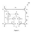
- FIG. 1 is a schematic diagram of a typical amplifier
- FIG. 2 is a schematic diagram of an embodiment of an amplifier, such as an amplifier in accordance with claimed subject matter
- FIG. 3 is a schematic diagram of an embodiment of a DC rejection circuit, such as may be employed in the embodiment of FIG. 2 , for example;
- FIG. 4 is a schematic diagram of an embodiment of a system that may employ an embodiment of a DC rejection circuit, such as the embodiment of FIG. 3 , for example;
- FIG. 5 is a schematic diagram of another embodiment of a DC rejection circuit, such as may be employed in the embodiment of FIG. 2 , for example;
- FIG. 6 is a schematic diagram of another embodiment of an amplifier such as in accordance with claimed subject matter.
- FIG. 7 is a plot of magnitude in decibel (dB) versus frequency in Hertz (Hz) and a plot of phase in degrees (deg) versus frequency (Hz) for an embodiment
- FIG. 8 shows two plots of input-referred noise (V/ ⁇ Hz) versus frequency (Hz) for an embodiment
- FIG. 9 is a plot of total harmonic distortion (THD) in percentage versus output amplitude in mV p-p for an embodiment
- FIG. 10 is a schematic diagram of an embodiment of a system that may employ an embodiment of an amplifier such as in accordance with claimed subject matter;
- FIG. 11 is a schematic diagram of an embodiment of an integrated circuit chip that may employ an embodiment of an amplifier such as in accordance with claimed subject matter;
- FIG. 12 is a schematic diagram illustrating the embodiment of FIG. 11 in more detail.
- FIG. 13 is a plot illustrating voltage versus time for an ideal amplifier and a non-ideal amplifier.
- batteries or other power sources may constitute a large portion of overall volume and/or weight of these devices, it may be desirable to reduce power consumption to prolong the life of the power source employed. Likewise, it may be desirable for these devices to operate with a light-weight and/or low-volume power source. Supply voltage and/or supply current, for example, may be reduced through the use of low-voltage, low-power circuits. However, in some medical applications, as one example, it may likewise be desirable to reduce noise or otherwise achieve low input referred noise to improve the quality of the signal.
- NEF V ni , r ⁇ ⁇ m ⁇ ⁇ s ⁇ 2 ⁇ I total ⁇ ⁇ U T ⁇ 4 ⁇ ⁇ ⁇ ⁇ ⁇ T ⁇ BW ( 1 )
- V ni,rms is the rms value of input-referred noise
- I total is the current consumption
- BW is the bandwidth in Hz.
- NEF for an “ideal” bipolar single-transistor amplifier in the absence of 1/f noise, NEF is 1.
- practical amplifiers have an NEF higher than 1.
- a lower NEF value is intended to indicate a better trade-off between current consumption and noise. It has been shown that for a CMOS chip through careful design an NEF of about 4.0 may be possible. See, for example, R. R. Harrison, C. Charles “A Low-Power Low-Noise CMOS Amplifier for Neural Recording Applications,” IEEE J. Solid State Circuits, vol. 38, no. 6, pp 958-965, June, 2003. This was achieved by carefully choosing transistor parameters. However, in the example, a supply voltage of about 5.0 V was employed.
- FIG. 1 is a schematic diagram of a typical amplifier, here an operational transconductance amplifier (OTA) with a differential input stage, referred to as amplifier 100 . It may be demonstrated that input-referred noise of 100 is:
- M 13 and M 14 in this particular embodiment comprise a common-mode load for M 11 and M 12 .
- the gate voltage of these former transistors in this embodiment, may be affected by a common-mode feedback (CMFB) circuit, illustrated in FIG. 2 and described in more detail hereinafter.
- CMFB common-mode feedback
- a common-mode feedback circuit for this particular embodiment may operate as follows. Such a circuit may have a configuration, one example being illustrated in FIG. 2 , so that it senses an average of a differential output voltage or a common-mode voltage change at the center of R 0 . Likewise, as illustrated, an output signal of a common-mode feedback circuit is applied to the gates of M 13 and M 14 and, therefore, may affect their operation. Likewise, the drains of these transistors are employed in this particular embodiment, here, so as to adjust a common-mode output voltage of the amplifier.
- a common mode input voltage range for this particular embodirrient may be described by the following relationship: V dsat3 +V thn +V dsat1 ⁇ V common ⁇ V cc ⁇ V dsat5 +V thn (8)
- a differential input voltage range may be related to bias current and R 1 .
- this may be described by the following relationship: ⁇ i 1 ⁇ R i ⁇ v in ⁇ i 1 ⁇ R i (9)
- noise may be reduced by employing a relatively large g m1 and a relatively small g m for the other transistors. This may be achieved, for example, by choosing appropriate aspect ratios (W/L).
- M 7 and M 8 employ a common gate configuration, as part of the previously described cascade configuration.
- Transistors M 1 and M 2 contribute little or negligible thermal and flicker noise.
- M 7 and M 8 are, therefore, not included in equations (10) and (11).
- aspect ratios of M 7 and M 8 may be made relatively large to reduce the overdrive voltage and provide more voltage headroom.
- small aspect ratios may assist in terms of low noise considerations.
- a limit exists in terms of how small the aspect ratios to be employed may become. This occurs at least in part from voltage headroom constraints related to low voltage operation.
- V dsat3 +V dsat7 +V dsat5 should not exceed (1 ⁇ V thn ), although claimed subject matter is not limited in scope in this respect, of course.
- M 7 and M 8 may become non-negligible if M 5 and M 6 operate near the edge of saturation region where output impedance decreases significantly.
- M 5 and M 6 are given enough margin in V DS to operate safely in the saturation region and have reasonably high output impedance for this particular embodiment.
- PMOS transistors generally exhibit low flicker noise and, of course, may be employed as input transistors.
- the threshold voltage of a PMOS transistor is about 0.2 V higher than that of an NMOS transistor.
- NMOS transistors are therefore chosen as the input transistors in the circuit of FIG. 2 , although, again, this is merely one example embodiment and claimed subject matter is not limited to this example.
- Relationships (10) and (11) imply that a small R i may be employed for relatively low noise operation.
- the input range is directly proportional to R i for a fixed bias current according to relationship (9). Therefore, trade-offs may exist among competing factors of noise, input range and power consumption.
- Some signals may include a DC component of several milli-volts in comparison with an AC component in a microvolt range. Thus, a reasonable portion of the dynamic range may be used to accommodate a DC component if that component is not removed. Likewise, for low voltage operation, voltage headroom is, in general, limited.
- a proposed DC rejection circuit is shown in FIG. 3 , together with an output stage of an amplifier, shown here without a common mode feedback (CMFB) circuit.
- a cut off frequency of 0.4 Hz is employed, which is implemented here by a 200-nF off-chip capacitor.
- the amount of input DC level that may be rejected depends at least partially on the dynamic range of current sources I 1 to I 4 .
- FIG. 6 shows a schematic drawing of an amplifier 600 .
- Amplifier 600 has an input stage 602 comprising transistors M 1 -M 10 and an output stage 604 comprising transistors M 11 -M 14 .
- M 1 to M 10 in this embodiment forms a series-shunt feedback loop for controlling respective gate voltages of a pair of transistors M 3 and M 4 of the input stage. Assuming output impedance of transistors M 1 -M 14 of 600 is sufficiently high, current flowing through M 1 and M 2 is substantially fixed at i bias1 ⁇ i bias2 .
- Input transistors M 1 and M 2 operate here as a differential voltage follower and the voltage across the resistor R i is V in .
- M 1 -M 10 and R i form a feedback loop which adjusts the gate voltages of M 3 and M 4 so that
- G m 2 R i ( 15 )
- the output signal of this g m cell is converted into a single-ended output signal by M 11 -M 14 .
- a comparison of FIGS. 1 and 6 shows that amplifier embodiment 600 replaces the differential-pair g m -cell in FIG. 1 with a g m -cell formed by M 1 -M 10 and R i .
- the transconductance g m9 and g m10 of M 9 and M 10 may be made lower than the transconductance of other transistors. Assuming that g m9 , g m10 ⁇ g m1 , g m5 and R i ⁇ 1/g m1 , relationship (16) becomes.
- amplifier 600 This difference between amplifier 600 and the known differential-pair-based amplifier of FIG. 1 may be desirable in at least some situations.
- a trade-off between noise performance and voltage-headroom is not necessary or present and is, therefore, not employed.
- this particular embodiment has the capability to achieve low-voltage, low-power, and low-noise performance, as well as a rail-rail output signal.
- claimed subject matter is not limited in scope to this particular embodiment or to these advantages; however, depending on the particular embodiment, such advantages may be present.
- FIG. 10 shows a battery operated electronic device 1000 comprising an amplifier 1002 .
- the device has amplifier 1002 coupled to an input unit 1004 for receiving input signals.
- the device 1000 also has amplifier 1002 coupled to an output unit 1006 for signal processing or other applications.
- a battery 1008 powers amplifier 1002 and may also power other active components of input unit 1004 and output unit 1006 .
- patients may benefit from wearable medical devices that provide real-time monitoring and/or possibly on-site treatment. It would be desirable for such devices to operate using a micro battery that is light-weight and low-volume, for example. Devices under such a constraint may operate, for example, at a low supply voltage, such as 1 ⁇ 1.5V, with ultra low power consumption for long battery lifetime, although, of course, this is merely an example and claimed subject matter is not limited in scope in this respect.
- a device exhibit low input referred noise.
- FIG. 11 One example embodiment of such a device is illustrated in FIG. 11 .
- the integrated circuit illustrated comprises a 1 V, 2.3 W biomedical signal acquisition IC.
- a low noise amplifier with DC rejection such as one of the embodiments previously described, may be employed.
- an 11-bit successive approximation ADC and other auxiliary circuits are included.
- V Dsat of M 11 -M 14 may be kept approximately below 50 mV, which enables rail-rail output swing up to about 850 mVp-p with total harmonic distortion (THD) approximately less than 1%.
- TDD total harmonic distortion
- the drain saturation voltages of the output transistors of the output stage are chosen for weak conversion operation and for substantially rail-rail output swing.
- an NEF of 4.0 may be achieved by using a known CMOS amplifier and setting an overdrive voltage of the output transistors approximately above 240 mV, this may be less desirable for a low-voltage design.
- a DC rejection circuit may be implemented using pseudo-resistors, as proposed in the aforementioned Harrison and Charles article.
- the ADC does not have a dedicated S/H circuit.
- the S/H operation may, instead, be performed through the output stage of the amplifier, which may be considered a pseudo S/H circuit.
- the amplifier is coupled directly to a capacitor array in the successive approximation ADC.
- two switches (SA and SB) in the output stage of the amplifier are turned off and the signal is held on the capacitor array of the ADC.
- SA and SB are turned on. Periodically switching the output stage may, however, introduce error.
- FIG. 12 illustrates A/D conversion
- T ADC represents the period of switching for the amplifier output stage for A/D conversion and T cycle is the sampling period.
- T cycle is sufficiently long and T ADC is sufficiently short, error attributable to switching should be small and nearly, if not completely, negligible.
- the sampling rate is 1 kS/s
- T cycle is 1 ms
- T ADC is 2 us, although, of course, these are merely examples and claimed subject matter is not limited in scope in this respect.
- a possible input-referred error for a typical ECG signal is less than ⁇ 0.3 uV, which is below this particular embodiment.
- ADCs typically employ a supply voltage higher than V thn +V thp to achieve a rail-rail input range.
- an alternate approach is employed, although claimed subject matter is again not limited in scope to this example embodiment.
- This particular embodiment achieves a rail-rail input range if a comparator common-mode input range encompasses V DD /2.
- ADC is inactive, the output signal of the amplifier is provided.
- S 1 is switched to V DD and S 2 ⁇ S 11 are switched to GND.
- Node C is charged to V in .
- the output stage is turned off and the voltage at node C successively approaches V DD /2 to perform ND conversion, as desired.
- an on-chip clock is generated by an 11-stage ring oscillator.
- Current-steering logic gates are chosen to reduce switching noise.
- the oscillator is turned on if the ADC is active, but otherwise is not.
- a start-up circuit as shown in FIG. 12 , may be employed for a substantially uniform start-up time for a conversion cycle. As an added precaution, the first dozen cycles of the oscillator after start-up may also be discarded.
- a dynamic comparator that does not consume power if inactive is employed to reduce power consumption.
- FIG. 7 shows a plot 702 of magnitude in decibels (dB) versus frequency in Hertz (Hz) and a plot 704 of phase in degrees (deg) versus frequency (Hz). From plot 702 , it can be observed that the magnitude increases from about 32 dB to about 40 dB, at which point the frequency increases from about 2 ⁇ 10 ⁇ 3 Hz to about 3 ⁇ 10 ⁇ 2 Hz. The magnitude remains about constant at a value of about 40 dB for a range of frequency from about 3 ⁇ 10 ⁇ 2 Hz to about 50 Hz. The magnitude then decreases from about 40 dB to about 20 dB as the frequency increases from about 50 Hz to about 1.8 ⁇ 10 3 Hz.
- the phase decreases from about 60 deg to about 10 deg as the frequency increases from about 2 ⁇ 10 ⁇ 3 Hz to about 3 ⁇ 10 ⁇ 2 Hz. There is a gradual decrease in the phase from about 10 deg to about 0 deg as the frequency increases from about 3 ⁇ 10 ⁇ 2 Hz to about 10 Hz. As the frequency increases from about 10 Hz to about 1.8 ⁇ 10 3 Hz, the phase decreases from about 0 deg to about ⁇ 130 deg.
- FIG. 8 shows plots 802 and 804 of input-referred noise (V/qHz) versus frequency (Hz).
- Plot 802 is obtained from measured input-referred noise while plot 804 is obtained from simulated input-referred noise.
- FIG. 9 shows a plot 902 of total harmonic distortion (THD) in percentage versus output amplitude in mV p-p .
- THD decreases from about 1.8% to about 0.1% as the output signal amplitude increases from about 0 to about 150 mV p-p .
- THD remains at roughly a constant value of about 0.1% for a range of output signal amplitude of about 150 mV p-p to 580 mV p-p .
- THD increases from about 0.1% to about 2.25% as output signal amplitude increases from about 580 mV p-p to about 920 mV p-p .
Abstract
Briefly, one or more embodiments of an amplifier, including example applications, are described.
Description
The present application is a divisional application of U.S. patent application Ser. No. 11/703,546, filed Feb. 5, 2007, entitled “AMPLIFIER,” which claims priority to U.S. Provisional Patent Application No. 60/765,057, filed Feb. 3, 2006, which are hereby incorporated by reference in their entireties for all purposes except for those sections, if any, that are inconsistent with the specification.
The present disclosure relates, in general, to amplifiers and similar electronic circuits. Portability is a desirable feature for a variety of electronic devices, including, for example, medical devices. Challenges exist in making electronic devices, such as amplifiers, for example, sufficiently small. One challenge relates to reducing power consumption since reduced power consumption may also reduce the size of a battery or similar power source to power the device. Likewise, a further challenge relates to noise reduction. At times, reducing power consumption may have an undesirable consequence in that signal quality may be reduced through increase noise.
Subject matter is particularly pointed out and distinctly claimed in the concluding portion of the specification. Claimed subject matter, however, both as to organization and method of operation, together with objects, features, and advantages thereof, may best be understood by reference of the following detailed description if read with the accompanying drawings in which:
In the following detailed description, numerous specific details are set forth to provide a thorough understanding of claimed subject matter. However, it will be understood by those skilled in the art that claimed subject matter may be practiced without these specific details. In other instances, well-known methods, procedures and/or other aspects have not been described in detail so as not to obscure claimed subject matter.
For example, medical devices for measuring electrocardiogram (ECG) or electroencephalogram (EEG) may be large and/or clumsy. For patients in which constant or regular ECG monitoring is desired, these medical devices may result in discomfort and/or inconvenience. Low-voltage low-power circuits may be employed for ECG and EEG devices. Thus, a potential exist for coin-sized devices to allow monitoring, while reducing discomfort and/or inconvenience for patients, for example.
Since batteries or other power sources may constitute a large portion of overall volume and/or weight of these devices, it may be desirable to reduce power consumption to prolong the life of the power source employed. Likewise, it may be desirable for these devices to operate with a light-weight and/or low-volume power source. Supply voltage and/or supply current, for example, may be reduced through the use of low-voltage, low-power circuits. However, in some medical applications, as one example, it may likewise be desirable to reduce noise or otherwise achieve low input referred noise to improve the quality of the signal.
Due at least in part to trade-offs between voltage headroom, current consumption and/or noise performance, achieving low-voltage, low-power, and/or low-noise performance in a single device or in a set of interoperating devices may be challenging. Typically, therefore, power consumption and noise performance are traded-off in a particular application. Noise efficiency factor (NEF), for example, which is a quantitative metric to measure the effectiveness of the trade off between current consumption and noise performance, has been proposed. In this particular context, NEF is defined as:
where Vni,rms is the rms value of input-referred noise, Itotal is the current consumption and BW is the bandwidth in Hz.
This measure is constructed so that for an “ideal” bipolar single-transistor amplifier in the absence of 1/f noise, NEF is 1. Thus, practical amplifiers have an NEF higher than 1. A lower NEF value is intended to indicate a better trade-off between current consumption and noise. It has been shown that for a CMOS chip through careful design an NEF of about 4.0 may be possible. See, for example, R. R. Harrison, C. Charles “A Low-Power Low-Noise CMOS Amplifier for Neural Recording Applications,” IEEE J. Solid State Circuits, vol. 38, no. 6, pp 958-965, June, 2003. This was achieved by carefully choosing transistor parameters. However, in the example, a supply voltage of about 5.0 V was employed.
For a device designed to achieve low NEF, unfortunately, the noise contribution from the input transistors may be dominant. FIG. 1 , for example, is a schematic diagram of a typical amplifier, here an operational transconductance amplifier (OTA) with a differential input stage, referred to as amplifier 100. It may be demonstrated that input-referred noise of 100 is:
Using relationship (2), one may infer that for a reduction in noise, transconductance of output transistors M3-M7 (gm3-7) should be smaller than transconductance of input transistor M1 (gm1). At a given bias current, aspect ratio (W/L) of the output transistors (M3-M7) may be reduced and aspect ratio (W/L) of the input transistors (M1 and M2) may be increased. However, choosing low aspect ratios for output transistors (M3-M7) may lead to a relatively high overdrive voltage (VGS-Vth) and a relatively high VDsat. At the output stage, a large portion of the voltage headroom may as a result be used to accommodate a high VDSat, which may detrimentally impact the ability of the output voltage to swing from rail-to-rail. Although increasing gm1, at a given bias current, should also reduce noise, typically gm1 cannot be arbitrarily increased. Thus, a trade-off between noise and voltage headroom typically results at the output stage of an amplifier.
However, FIG. 2 shows a schematic diagram of an embodiment of an amplifier, here, amplifier 200. Although claimed subject matter is not limited in scope in this respect, amplifier 200 may be employed to provide a relatively low-noise signal while employing relatively low power. In FIG. 2 , transistors M1-M12 form a relatively low voltage gm cell, as explained in more detail below. There are two bias current sources provided off-chip, here Ibias1 and Ibias2. In the cell, M1 and M2 are NMOS transistors having sufficiently similar characteristics to cooperate to form a voltage follower with a resistor joining the sources of M1 and M2. Thus, input voltage Vin, comprising (Vin+, Vin−) is applied to Ri. The resultant current flowing through Ri is:
i Ri =v in /R i (3)
i R
For the embodiment shown in FIG. 2 , transistors M1-M10 form a series-shunt feedback loop to adjust gate voltages of M3 and M4 so that electric currents passing through transistors M3, M1, M4 and resistor Ri may be described as follows:
i 3 =i 1 −i R1 (4)
and
i 4 =i 1 +i R1 (5)
i 3 =i 1 −i R
and
i 4 =i 1 +i R
In FIG. 2 , M3, M4, M11 and M12 have sufficiently similar size for appropriate mirroring. Drain currents of M3 and M4 are applied to M11 and M12 as a result. The transconductance of the cell of this embodiment, therefore, may be described by the following relationship:
g m,cell=(i 12 −i 11)/v in=(i 4 −i 3)/v in=2/R i (6)
g m,cell=(i 12 −i 11)/v in=(i 4 −i 3)/v in=2/R i (6)
M13 and M14 in this particular embodiment comprise a common-mode load for M11 and M12. Likewise, the gate voltage of these former transistors, in this embodiment, may be affected by a common-mode feedback (CMFB) circuit, illustrated in FIG. 2 and described in more detail hereinafter.
Differential current flowing through Ro is (i12−i11)/2 and voltage gain of the cell for this particular embodiment may be described by the following relationship:
Although claimed subject matter is not limited in scope in this respect, a common-mode feedback circuit for this particular embodiment may operate as follows. Such a circuit may have a configuration, one example being illustrated in
For this particular embodiment, as illustrated, M5 and M6 provide bias currents for M1 and M2, and M7 and M8, respectively. M1 and M2, and M7 and M8 form a differential cascode configuration with M9 and M10 as the load. A cascode configuration here operates to provide high gain for the feedback loop of this particular embodiment. Likewise, the output signal of this cascode configuration is fed back through M3 and M4.
A common mode input voltage range for this particular embodirrient may be described by the following relationship:
V dsat3 +V thn +V dsat1 <V common <V cc −V dsat5 +V thn (8)
V dsat3 +V thn +V dsat1 <V common <V cc −V dsat5 +V thn (8)
A differential input voltage range may be related to bias current and R1. For this particular embodiment, for example, this may be described by the following relationship:
−i 1 ·R i <v in <i 1 ·R i (9)
−i 1 ·R i <v in <i 1 ·R i (9)
To evaluate noise and low voltage aspects of this particular embodiment, illustrated in FIG. 2 , a simplified noise analysis may be employed. For this embodiment, input referred thermal noise contributed by M1-M14, Rin and Rout may be described by the following relationship:
The input referred flicker noise from M1-M14 may be described by the following relationship:
where
From relationships (10) and (11), one may infer that noise may be reduced by employing a relatively large gm1 and a relatively small gm for the other transistors. This may be achieved, for example, by choosing appropriate aspect ratios (W/L).
M7 and M8 employ a common gate configuration, as part of the previously described cascade configuration. Transistors M1 and M2 contribute little or negligible thermal and flicker noise. M7 and M8 are, therefore, not included in equations (10) and (11). Thus, aspect ratios of M7 and M8 may be made relatively large to reduce the overdrive voltage and provide more voltage headroom. For M3-M6 and M9-M14, small aspect ratios may assist in terms of low noise considerations. However, a limit exists in terms of how small the aspect ratios to be employed may become. This occurs at least in part from voltage headroom constraints related to low voltage operation.
More specifically, power supply voltage may be described from the following relationship:
V cc,min =V thn +V dsat3 +V dsat3 +V dsat1 +V dsat5 (13)
where VDsat is the overdrive voltage. According to relationship (13), for a 1-V supply, for example, Vdsat3+Vdsat7+Vdsat5 should not exceed (1−Vthn), although claimed subject matter is not limited in scope in this respect, of course.
V cc,min =V thn +V dsat3 +V dsat3 +V dsat1 +V dsat5 (13)
where VDsat is the overdrive voltage. According to relationship (13), for a 1-V supply, for example, Vdsat3+Vdsat7+Vdsat5 should not exceed (1−Vthn), although claimed subject matter is not limited in scope in this respect, of course.
Moreover, the noise contribution of M7 and M8 may become non-negligible if M5 and M6 operate near the edge of saturation region where output impedance decreases significantly. Thus, M5 and M6 are given enough margin in VDS to operate safely in the saturation region and have reasonably high output impedance for this particular embodiment. PMOS transistors generally exhibit low flicker noise and, of course, may be employed as input transistors. However, in a targeted CMOS process, the threshold voltage of a PMOS transistor is about 0.2 V higher than that of an NMOS transistor. For this particular embodiment in which low voltage operation is desired, NMOS transistors are therefore chosen as the input transistors in the circuit of FIG. 2 , although, again, this is merely one example embodiment and claimed subject matter is not limited to this example.
Relationships (10) and (11) imply that a small Ri may be employed for relatively low noise operation. On the other hand, the input range is directly proportional to Ri for a fixed bias current according to relationship (9). Therefore, trade-offs may exist among competing factors of noise, input range and power consumption.
Some signals, such as signals employed in medical applications, for example, may include a DC component of several milli-volts in comparison with an AC component in a microvolt range. Thus, a reasonable portion of the dynamic range may be used to accommodate a DC component if that component is not removed. Likewise, for low voltage operation, voltage headroom is, in general, limited.
Thus, a proposed DC rejection circuit is shown in FIG. 3 , together with an output stage of an amplifier, shown here without a common mode feedback (CMFB) circuit. This circuit may comprise a high-pass filter implemented by a frequency selective feedback network, as illustrated in FIG. 4 , where iin is iRo in the absence of a DC rejection circuit. More specifically, for this particular embodiment, iin=(i11−i12)/2 and iout is iRo in the presence of a DC rejection circuit. For this embodiment, a cut off frequency of 0.4 Hz is employed, which is implemented here by a 200-nF off-chip capacitor. The amount of input DC level that may be rejected depends at least partially on the dynamic range of current sources I1 to I4. To address the issue of potentially draining too much current, high values of I1 to I4 are set to 4 μA. This translates into a corresponding input DC level of ±11 mV, which is sufficient for the present application. Since here the DC rejection circuit works in the current domain, it does not require much voltage headroom to operate, which is one advantage of this particular embodiment of a DC rejection circuit, although claimed subject matter is not limited in scope in this respect. An example of another implementation of a DC rejection circuit is shown in FIG. 5 .
Equation (14) suggests that M1-M10 and Ri form a gm-cell with its transconductance being
The output signal of this gm cell is converted into a single-ended output signal by M11-M14. A comparison of
Noise analysis shows that the input referred thermal noise of amplifier 600 is
where K=(W/L)11/(W/L)3. Since the drain voltages of M9 and M10 are relatively high (VDS9=VGS3) and biased at a low current, the transconductance gm9 and gm10 of M9 and M10 may be made lower than the transconductance of other transistors. Assuming that gm9, gm10<<gm1, gm5 and Ri<<1/gm1, relationship (16) becomes.
Relationship (17) suggests that noise contribution from output transistors M11-M14 is not substantially dependent on the transconductance of the input transistors, such as gm1, for example, but is at least partially dependent on Gm instead.
This difference between amplifier 600 and the known differential-pair-based amplifier of FIG. 1 may be desirable in at least some situations. For example, for amplifier 600, a trade-off between noise performance and voltage-headroom is not necessary or present and is, therefore, not employed. This permits a rail-rail output signal for a low supply voltage, for example, without significant signal degradation. Thus, this particular embodiment has the capability to achieve low-voltage, low-power, and low-noise performance, as well as a rail-rail output signal. Of course, claimed subject matter is not limited in scope to this particular embodiment or to these advantages; however, depending on the particular embodiment, such advantages may be present.
It should be noted that according to relationship (16), a noise-voltage headroom trade off exists in input stage 602 of amplifier 600. Transconductance gm5 and gm9 may therefore be employed to achieve low input-referred noise. However, since voltage swing is low in input stage 602, this trade-off is tolerable.
The amplifier embodiment as described above can be used for a large variety of applications in which low voltage, low power and low noise are desired, including in portable medical devices, such as devices for electrocardiogram (ECG) or electroencephalogram (EEG), although, of course, claimed subject matter is not limited in scope in this respect. For example, FIG. 10 shows a battery operated electronic device 1000 comprising an amplifier 1002. The device has amplifier 1002 coupled to an input unit 1004 for receiving input signals. The device 1000 also has amplifier 1002 coupled to an output unit 1006 for signal processing or other applications. A battery 1008 powers amplifier 1002 and may also power other active components of input unit 1004 and output unit 1006.
In one potential application, patients, for example, may benefit from wearable medical devices that provide real-time monitoring and/or possibly on-site treatment. It would be desirable for such devices to operate using a micro battery that is light-weight and low-volume, for example. Devices under such a constraint may operate, for example, at a low supply voltage, such as 1˜1.5V, with ultra low power consumption for long battery lifetime, although, of course, this is merely an example and claimed subject matter is not limited in scope in this respect. In addition, to pick up potentially weak biomedical signals, it may be desirable that a device exhibit low input referred noise. One example embodiment of such a device is illustrated in FIG. 11 . The integrated circuit illustrated comprises a 1 V, 2.3 W biomedical signal acquisition IC. Here, a low noise amplifier with DC rejection, such as one of the embodiments previously described, may be employed. Likewise, an 11-bit successive approximation ADC and other auxiliary circuits are included.
This example implementation was fabricated in a 0.35 μm process. Test results show that a resulting amplifier consumes about 330 nA at a supply voltage of approximately 1 V while input referred noise is about 2.7 μVrms (integrated up to about 245 Hz), which gives an NEF of about 3.8. For a fair comparison with the previously described known CMOS amplifier of R. R. Harrison, C. Charles “A Low-Power Low-Noise CMOS Amplifier for Neural Recording Applications,” IEEE J. Solid State Circuits, vol. 38, no. 6, pp 958-965, June, 2003, bias consumption is excluded from the NEF calculation. VDsat of M11-M14 may be kept approximately below 50 mV, which enables rail-rail output swing up to about 850 mVp-p with total harmonic distortion (THD) approximately less than 1%. In other words, the drain saturation voltages of the output transistors of the output stage are chosen for weak conversion operation and for substantially rail-rail output swing. Thus, while an NEF of 4.0 may be achieved by using a known CMOS amplifier and setting an overdrive voltage of the output transistors approximately above 240 mV, this may be less desirable for a low-voltage design.
As illustrated in FIG. 11 , a DC rejection circuit may be implemented using pseudo-resistors, as proposed in the aforementioned Harrison and Charles article. To conserve power, for this particular embodiment, the ADC does not have a dedicated S/H circuit. The S/H operation may, instead, be performed through the output stage of the amplifier, which may be considered a pseudo S/H circuit. As shown in FIG. 12 , the amplifier is coupled directly to a capacitor array in the successive approximation ADC. During A/D conversion, two switches (SA and SB) in the output stage of the amplifier are turned off and the signal is held on the capacitor array of the ADC. After A/D conversion, SA and SB are turned on. Periodically switching the output stage may, however, introduce error. As illustrated in FIG. 13 , TADC represents the period of switching for the amplifier output stage for A/D conversion and Tcycle is the sampling period. Applying a first-order model to this particular embodiment, as illustrated in FIG. 13 , if Tcycle is sufficiently long and TADC is sufficiently short, error attributable to switching should be small and nearly, if not completely, negligible. In this particular embodiment, the sampling rate is 1 kS/s, Tcycle is 1 ms and TADC is 2 us, although, of course, these are merely examples and claimed subject matter is not limited in scope in this respect. A possible input-referred error for a typical ECG signal is less than ±0.3 uV, which is below this particular embodiment.
Conventional capacitor-array-based successive approximation ADCs typically employ a supply voltage higher than Vthn+Vthp to achieve a rail-rail input range. In this particular embodiment, an alternate approach is employed, although claimed subject matter is again not limited in scope to this example embodiment. This particular embodiment achieves a rail-rail input range if a comparator common-mode input range encompasses VDD/2. If ADC is inactive, the output signal of the amplifier is provided. In this embodiment, S1 is switched to VDD and S2˜S11 are switched to GND. Node C is charged to Vin. During A/D conversion, the output stage is turned off and the voltage at node C successively approaches VDD/2 to perform ND conversion, as desired. Here, an on-chip clock is generated by an 11-stage ring oscillator. Current-steering logic gates are chosen to reduce switching noise. To conserve power, the oscillator is turned on if the ADC is active, but otherwise is not. A start-up circuit, as shown in FIG. 12 , may be employed for a substantially uniform start-up time for a conversion cycle. As an added precaution, the first dozen cycles of the oscillator after start-up may also be discarded. Likewise, in this embodiment, as illustrated, a dynamic comparator that does not consume power if inactive is employed to reduce power consumption.
Further results are described with reference to FIGS. 7-9 . FIG. 7 shows a plot 702 of magnitude in decibels (dB) versus frequency in Hertz (Hz) and a plot 704 of phase in degrees (deg) versus frequency (Hz). From plot 702, it can be observed that the magnitude increases from about 32 dB to about 40 dB, at which point the frequency increases from about 2×10⁻³ Hz to about 3×10⁻² Hz. The magnitude remains about constant at a value of about 40 dB for a range of frequency from about 3×10⁻² Hz to about 50 Hz. The magnitude then decreases from about 40 dB to about 20 dB as the frequency increases from about 50 Hz to about 1.8×10³ Hz.
From plot 704, it may be observed that the phase decreases from about 60 deg to about 10 deg as the frequency increases from about 2×10⁻³ Hz to about 3×10⁻² Hz. There is a gradual decrease in the phase from about 10 deg to about 0 deg as the frequency increases from about 3×10⁻² Hz to about 10 Hz. As the frequency increases from about 10 Hz to about 1.8×10³ Hz, the phase decreases from about 0 deg to about −130 deg.
In the preceding description, various aspects of claimed subject matter have been described. For purposes of explanation, specific numbers, systems and/or configurations were set forth to provide a thorough understanding of claimed subject matter. However, it should be apparent to one skilled in the art having the benefit of this disclosure that claimed subject matter may be practiced without the specific details. In other instances, well known features were omitted and/or simplified so as not to obscure claimed subject matter. While certain features have been illustrated and/or described herein, many modifications, substitutions, changes and/or equivalents will now occur to those skilled in the art. It is, therefore, to be understood that the appended claims are intended to cover all such modifications and/or changes as fall within the true spirit of claimed subject matter.
Claims (23)
1. An apparatus for amplifying a differential voltage signal, comprising:
an amplifier configured to remove a DC voltage signal component from the differential voltage signal to provide an analog output voltage signal; and
a successive approximation analog-to-digital converter (ADC) coupled to an output of the amplifier and configured to convert the analog output voltage signal to a digital signal;
further comprising an oscillator to provide a clock signal, wherein the oscillator is coupled to be turned on if the ADC is active and turned off otherwise.
2. The apparatus of claim 1 , wherein the ADC comprises an 11 bit ADC.
3. The apparatus of claim 1 , wherein the IC is adapted to operate with a one volt power source.
4. An apparatus for amplifying a differential voltage signal, comprising:
an amplifier configured to remove a DC voltage signal component from the differential voltage signal to provide an analog output voltage signal; and
a successive approximation analog-to-digital converter (ADC) coupled to an output of the amplifier and configured to convert the analog output voltage signal to a digital signal;
wherein the amplifier includes a DC rejection circuit implemented using at least one pseudo-resistor.
5. An apparatus for amplifying a differential voltage signal, comprising:
an amplifier configured to remove a DC voltage signal component from the differential voltage signal to provide an analog output voltage signal; and
a successive approximation analog-to-digital converter (ADC) coupled to an output of the amplifier and configured to convert the analog output voltage signal to a digital signal;
wherein the amplifier and the ADC are coupled so as to provide a pseudo-sample and hold circuit.
6. An apparatus for amplifying a differential voltage signal, comprising:
an amplifier configured to remove a DC voltage signal component from the differential voltage signal to provide an analog output voltage signal, wherein the amplifier comprises:
an input stage comprising a series-shunt feedback loop for controlling respective gate voltages of a first pair of transistors of the input stage; and
an output stage coupled to the first pair of transistors of the input stage such that respective gates of a first pair of transistors of the output stage are coupled to the respective gates of the first pair of transistors of the input stage; and
a successive approximation analog-to-digital converter (ADC) coupled to an output of the amplifier and configured to convert the analog output voltage signal to a digital signal.
7. The apparatus of claim 6 , wherein the output stage is configured to provide a substantially rail-to-rail analog output voltage signal without significantly increasing noise in the analog output voltage signal.
8. The apparatus of claim 7 , wherein the input stage comprises a second pair of transistors, wherein gates of the second pair of transistors of the input stage are coupled to receive the differential voltage signal, and wherein sources of the second pair of transistors of the input stage are coupled to respective drains of the first pair of transistors of the input stage.
9. The apparatus of claim 8 , wherein the feedback loop comprises a resistor coupled between the sources of the second pair of transistors of the input stage.
10. The apparatus of claim 9 , wherein the feedback loop further comprises a third pair of transistors in a cascade configuration with the second pair of transistors of the input stage.
11. The apparatus of claim 6 , wherein the output stage comprises a second pair of transistors forming a common-mode load for the first pair of transistors of the output stage.
12. The apparatus of claim 11 , further comprising a common-mode feedback circuit coupled to gates of the second pair of transistors of the output stage.
13. The apparatus of claim 12 , further comprising a resistor coupled between the drains of the second pair of transistors of the output stage, wherein the common-mode feedback circuit is configured to sense a voltage at the resistor.
14. The apparatus of claim 6 , further comprising a DC rejection circuit coupled to the output stage.
15. The apparatus of claim 1 , wherein the apparatus is a battery operated electronic device.
16. The apparatus of claim 1 , wherein the amplifier and the ADC are incorporated into an integrated circuit chip.
17. The apparatus of claim 1 , wherein the apparatus is a medical device.
18. The apparatus of claim 17 , wherein the medical device is an electroencephalogram or an electrocardiogram.
19. The apparatus of claim 1 , wherein the apparatus is a low noise operational transconductance amplifier (LN-OTA).
20. The apparatus of claim 19 , further comprising:
an input unit configured to receive signals; an output unit configured to output signals; and
a battery configured to power the LN-OTA.
21. A method comprising:
amplifying a differential voltage signal including rejecting a DC component to provide an analog output voltage signal;
converting the analog output voltage signal to a digital signal by successive approximation; and
turning on an oscillator to provide a clock signal, and turning off the oscillator if said converting stops.
22. The method of claim 21 , further comprising providing a substantially rail-to-rail analog output voltage signal from a one volt power source without significantly increasing noise in the analog output voltage signal.
23. A method comprising:
amplifying a differential voltage signal including rejecting a DC component to provide an analog output voltage signal;
converting the analog output voltage signal to a digital signal by successive approximation; and
sampling and holding the analog output voltage signal to initiate said converting.
Priority Applications (1)
| Application Number | Priority Date | Filing Date | Title |
|---|---|---|---|
| US12/896,661 US8072269B2 (en) | 2006-02-03 | 2010-10-01 | Amplifier |
Applications Claiming Priority (3)
| Application Number | Priority Date | Filing Date | Title |
|---|---|---|---|
| US76505706P | 2006-02-03 | 2006-02-03 | |
| US11/703,546 US7816988B2 (en) | 2006-02-03 | 2007-02-05 | Amplifier |
| US12/896,661 US8072269B2 (en) | 2006-02-03 | 2010-10-01 | Amplifier |
Related Parent Applications (1)
| Application Number | Title | Priority Date | Filing Date |
|---|---|---|---|
| US11/703,546 Division US7816988B2 (en) | 2006-02-03 | 2007-02-05 | Amplifier |
Publications (2)
| Publication Number | Publication Date |
|---|---|
| US20110074616A1 US20110074616A1 (en) | 2011-03-31 |
| US8072269B2 true US8072269B2 (en) | 2011-12-06 |
Family
ID=38532735
Family Applications (2)
| Application Number | Title | Priority Date | Filing Date |
|---|---|---|---|
| US11/703,546 Active 2028-01-26 US7816988B2 (en) | 2006-02-03 | 2007-02-05 | Amplifier |
| US12/896,661 Active US8072269B2 (en) | 2006-02-03 | 2010-10-01 | Amplifier |
Family Applications Before (1)
| Application Number | Title | Priority Date | Filing Date |
|---|---|---|---|
| US11/703,546 Active 2028-01-26 US7816988B2 (en) | 2006-02-03 | 2007-02-05 | Amplifier |
Country Status (1)
| Country | Link |
|---|---|
| US (2) | US7816988B2 (en) |
Cited By (3)
| Publication number | Priority date | Publication date | Assignee | Title |
|---|---|---|---|---|
| US8659340B2 (en) * | 2011-09-16 | 2014-02-25 | National Central University | Tunable voltage-controlled pseudo-resistor |
| US20180212577A1 (en) * | 2017-01-26 | 2018-07-26 | Analog Devices, Inc. | Common mode feedback circuit with backgate control |
| US20190131462A1 (en) * | 2017-10-31 | 2019-05-02 | Imec Vzw | Pseudo-resistor structure, a closed-loop operational amplifier circuit and a bio-potential sensor |
Families Citing this family (4)
| Publication number | Priority date | Publication date | Assignee | Title |
|---|---|---|---|---|
| US8384421B1 (en) * | 2011-04-21 | 2013-02-26 | Applied Micro Circuits Corporation | Digital CMOS circuit with noise cancellation |
| KR101190811B1 (en) | 2011-05-25 | 2012-10-15 | 한국과학기술연구원 | A tunable band-pass filter for multi-biopotential signal processing system |
| US9356570B2 (en) * | 2014-05-15 | 2016-05-31 | Texas Instruments Deutschland Gmbh | High speed, rail-to-rail CMOS differential input stage |
| ITUB20159451A1 (en) * | 2015-12-15 | 2017-06-15 | St Microelectronics Srl | DIFFERENTIAL AMPLIFIER WITH COMMON MODE COMPENSATION CIRCUIT |
Citations (28)
| Publication number | Priority date | Publication date | Assignee | Title |
|---|---|---|---|---|
| US4519401A (en) | 1983-09-20 | 1985-05-28 | Case Western Reserve University | Pressure telemetry implant |
| US4590458A (en) * | 1985-03-04 | 1986-05-20 | Exxon Production Research Co. | Offset removal in an analog to digital conversion system |
| US5272481A (en) | 1991-07-02 | 1993-12-21 | David Sarnoff Research Center, Inc. | Successive approximation analog to digital converter employing plural feedback digital to analog converters |
| US6118400A (en) | 1998-01-20 | 2000-09-12 | Microchip Technology Incorporated | Capacitor array for a successive approximation register (SAR) based analog to digital (A/D) converter and method therefor |
| US6124818A (en) | 1998-10-21 | 2000-09-26 | Linear Technology Corporation | Pipelined successive approximation analog-to-digital converters |
| US6201489B1 (en) * | 2000-03-21 | 2001-03-13 | International Business Machines Corporation | Method and circuit for temporal cancellation of DC offset |
| US6262563B1 (en) * | 1998-09-11 | 2001-07-17 | Keith S. Champlin | Method and apparatus for measuring complex admittance of cells and batteries |
| US6300669B1 (en) | 1997-09-29 | 2001-10-09 | Nec Corporation | Semiconductor integrated circuit device and method of designing same |
| US6307430B1 (en) | 2000-10-02 | 2001-10-23 | Cirrus Logic, Inc. | Noise reduction technique in chopper stabilized amplifier |
| US6480042B2 (en) | 2000-07-04 | 2002-11-12 | Matsushita Electric Industrial Co., Ltd. | Current-to-voltage converting circuit, optical pickup head apparatus, and apparatus and method for recording/reproducing data |
| US20030155966A1 (en) | 2002-02-20 | 2003-08-21 | Harrison Reid R. | Low-power, low-noise CMOS amplifier |
| US6756924B2 (en) * | 2002-05-16 | 2004-06-29 | Integrant Technologies Inc. | Circuit and method for DC offset calibration and signal processing apparatus using the same |
| US6831690B1 (en) | 1999-12-07 | 2004-12-14 | Symagery Microsystems, Inc. | Electrical sensing apparatus and method utilizing an array of transducer elements |
| US6850753B2 (en) | 2002-06-11 | 2005-02-01 | Muchip Co., Ltd | Tunable low noise amplifier and current-reused mixer for a low power RF application |
| US6909327B2 (en) | 2001-05-18 | 2005-06-21 | Rohm Co., Ltd. | Amplifier |
| US6973182B1 (en) | 2003-03-10 | 2005-12-06 | National Semiconductor Corporation | Differential echo cancellation receiver with dynamic cancellation of excess DC output current |
| US7020513B2 (en) * | 2002-01-23 | 2006-03-28 | Ela Medical S.A. | Testing the electrical continuity of the connecting cables for a recorder of physiological signals, in particular a holter recorder of ECG signals |
| US7068319B2 (en) | 2002-02-01 | 2006-06-27 | Micron Technology, Inc. | CMOS image sensor with a low-power architecture |
| US7071778B2 (en) | 2003-04-28 | 2006-07-04 | Sony Corporation | High-speed low-power dynamic current biased operational amplifier |
| US7126403B2 (en) | 2004-11-01 | 2006-10-24 | Analog Devices, Inc. | LC tank clock driver with automatic tuning |
| US7215198B1 (en) | 2004-06-01 | 2007-05-08 | Marvell International Ltd. | Fully differential current-feedback CMOS/bipolar operational amplifier |
| US7250896B1 (en) | 2006-06-01 | 2007-07-31 | Infineon Technologies Ag | Method for pipelining analog-to-digital conversion and a pipelining analog-to-digital converter with successive approximation |
| US7256725B2 (en) | 2002-05-24 | 2007-08-14 | Broadcom Corporation | Resistor ladder interpolation for subranging ADC |
| US7324035B2 (en) | 2004-05-13 | 2008-01-29 | University Of Florida Research Foundation, Inc. | Amplifier with pulse coded output and remote signal reconstruction from the pulse output |
| US20080030271A1 (en) | 2004-06-25 | 2008-02-07 | Niigata Seimitsu Co., Ltd. | Stereo Separation Adjustment Circuit And Mos Integrated Circuit Thereof |
| US7405689B2 (en) | 2005-01-05 | 2008-07-29 | Exar Corporation | Predictive analog to digital converters and methods of using |
| US7427738B2 (en) | 2005-10-31 | 2008-09-23 | Sharp Kabushiki Kaisha | Light-receiving amplifier and optical pickup device |
| US7605646B2 (en) * | 2007-07-06 | 2009-10-20 | Texas Instruments Incorporated | Low glitch offset correction circuit for auto-zero sensor amplifiers and method |
-
2007
- 2007-02-05 US US11/703,546 patent/US7816988B2/en active Active
-
2010
- 2010-10-01 US US12/896,661 patent/US8072269B2/en active Active
Patent Citations (28)
| Publication number | Priority date | Publication date | Assignee | Title |
|---|---|---|---|---|
| US4519401A (en) | 1983-09-20 | 1985-05-28 | Case Western Reserve University | Pressure telemetry implant |
| US4590458A (en) * | 1985-03-04 | 1986-05-20 | Exxon Production Research Co. | Offset removal in an analog to digital conversion system |
| US5272481A (en) | 1991-07-02 | 1993-12-21 | David Sarnoff Research Center, Inc. | Successive approximation analog to digital converter employing plural feedback digital to analog converters |
| US6300669B1 (en) | 1997-09-29 | 2001-10-09 | Nec Corporation | Semiconductor integrated circuit device and method of designing same |
| US6118400A (en) | 1998-01-20 | 2000-09-12 | Microchip Technology Incorporated | Capacitor array for a successive approximation register (SAR) based analog to digital (A/D) converter and method therefor |
| US6262563B1 (en) * | 1998-09-11 | 2001-07-17 | Keith S. Champlin | Method and apparatus for measuring complex admittance of cells and batteries |
| US6124818A (en) | 1998-10-21 | 2000-09-26 | Linear Technology Corporation | Pipelined successive approximation analog-to-digital converters |
| US6831690B1 (en) | 1999-12-07 | 2004-12-14 | Symagery Microsystems, Inc. | Electrical sensing apparatus and method utilizing an array of transducer elements |
| US6201489B1 (en) * | 2000-03-21 | 2001-03-13 | International Business Machines Corporation | Method and circuit for temporal cancellation of DC offset |
| US6480042B2 (en) | 2000-07-04 | 2002-11-12 | Matsushita Electric Industrial Co., Ltd. | Current-to-voltage converting circuit, optical pickup head apparatus, and apparatus and method for recording/reproducing data |
| US6307430B1 (en) | 2000-10-02 | 2001-10-23 | Cirrus Logic, Inc. | Noise reduction technique in chopper stabilized amplifier |
| US6909327B2 (en) | 2001-05-18 | 2005-06-21 | Rohm Co., Ltd. | Amplifier |
| US7020513B2 (en) * | 2002-01-23 | 2006-03-28 | Ela Medical S.A. | Testing the electrical continuity of the connecting cables for a recorder of physiological signals, in particular a holter recorder of ECG signals |
| US7068319B2 (en) | 2002-02-01 | 2006-06-27 | Micron Technology, Inc. | CMOS image sensor with a low-power architecture |
| US20030155966A1 (en) | 2002-02-20 | 2003-08-21 | Harrison Reid R. | Low-power, low-noise CMOS amplifier |
| US6756924B2 (en) * | 2002-05-16 | 2004-06-29 | Integrant Technologies Inc. | Circuit and method for DC offset calibration and signal processing apparatus using the same |
| US7256725B2 (en) | 2002-05-24 | 2007-08-14 | Broadcom Corporation | Resistor ladder interpolation for subranging ADC |
| US6850753B2 (en) | 2002-06-11 | 2005-02-01 | Muchip Co., Ltd | Tunable low noise amplifier and current-reused mixer for a low power RF application |
| US6973182B1 (en) | 2003-03-10 | 2005-12-06 | National Semiconductor Corporation | Differential echo cancellation receiver with dynamic cancellation of excess DC output current |
| US7071778B2 (en) | 2003-04-28 | 2006-07-04 | Sony Corporation | High-speed low-power dynamic current biased operational amplifier |
| US7324035B2 (en) | 2004-05-13 | 2008-01-29 | University Of Florida Research Foundation, Inc. | Amplifier with pulse coded output and remote signal reconstruction from the pulse output |
| US7215198B1 (en) | 2004-06-01 | 2007-05-08 | Marvell International Ltd. | Fully differential current-feedback CMOS/bipolar operational amplifier |
| US20080030271A1 (en) | 2004-06-25 | 2008-02-07 | Niigata Seimitsu Co., Ltd. | Stereo Separation Adjustment Circuit And Mos Integrated Circuit Thereof |
| US7126403B2 (en) | 2004-11-01 | 2006-10-24 | Analog Devices, Inc. | LC tank clock driver with automatic tuning |
| US7405689B2 (en) | 2005-01-05 | 2008-07-29 | Exar Corporation | Predictive analog to digital converters and methods of using |
| US7427738B2 (en) | 2005-10-31 | 2008-09-23 | Sharp Kabushiki Kaisha | Light-receiving amplifier and optical pickup device |
| US7250896B1 (en) | 2006-06-01 | 2007-07-31 | Infineon Technologies Ag | Method for pipelining analog-to-digital conversion and a pipelining analog-to-digital converter with successive approximation |
| US7605646B2 (en) * | 2007-07-06 | 2009-10-20 | Texas Instruments Incorporated | Low glitch offset correction circuit for auto-zero sensor amplifiers and method |
Non-Patent Citations (15)
| Title |
|---|
| Harrison et al., "A Low-Power Low-Noise CMOS Amplifier for Neural Recording Applications," IEEE Journal of Solid-State Circuite, vol. 38, No. 6, Jun. 2003, Salt Lake City, UT. |
| Holleman et al., "A Sub-Microwatt Low-Noise Amplifier for Neural Recording," FrD05.1, 29th Annual International Conference of the IEEE EMBS , Aug. 23-26, 2007, Lyon, France. |
| Hu et al., "CMOS Front-end Amplifier Dedicated to Monitor Very Low Amplitude Signal from Implantable Sensors," IEEE Midwest Symposium on Circuits and Systems, Lansing MI, Aug. 8-11, 2000. |
| Martins et al., "A CMOS IC for Portable EEG Acquisition System," IEEE Transactions on Instrumentation and Measurement, vol. 47, No. 5, Oct. 1998, Portugal. |
| Nielsen et al., "A Low-Power 10-Bit Continuous-Time CMOS SigmaDelta A/D Converter," 2004 IEEE, ISCAS 2004, Technical University of Denmark. |
| Nielsen et al., "A Low-Power 10-Bit Continuous-Time CMOS ΣΔ A/D Converter," 2004 IEEE, ISCAS 2004, Technical University of Denmark. |
| Notice of Allowance mailed Jun. 15, 2010 in U.S. Appl. No. 11/703,546. |
| Office Action mailed Dec. 31, 2009 in U.S. Appl. No. 11/703,546. |
| Office Action mailed Jun. 18, 2009 in U.S. Appl. No. 11/703,546. |
| Office Action mailed Sep. 26, 2008 in U.S. Appl. No. 11/703,546. |
| Steyaert et al., "A Micropower Low-Noise Monolithic Instrumentation Amplifier for Medical Purposes," IEEE Journal of Solid-State Circuits, vol. SC-22, No. 6, Dec. 1987. |
| Uranga et al., "A Low Noise CMOS Amplifier for Eng Signals," IEEE, ISCAS 2004, Spain. |
| Wu et al., "A 1V 2.3muW Biomedical Signal Acquisition IC," 2006 IEEE International Solid-State Circuits Conference, ISSCC 2006/Session 2/Biomedical Systems/2.7. |
| Wu et al., "A 1V 2.3μW Biomedical Signal Acquisition IC," 2006 IEEE International Solid-State Circuits Conference, ISSCC 2006/Session 2/Biomedical Systems/2.7. |
| Wu et al., "A Low-Voltage Low-Noise CMOS Instrumentation Amplifier for Portable Medical Monitoring Systems," 2005 IEEE, National University of Singapore, Singapore. |
Cited By (5)
| Publication number | Priority date | Publication date | Assignee | Title |
|---|---|---|---|---|
| US8659340B2 (en) * | 2011-09-16 | 2014-02-25 | National Central University | Tunable voltage-controlled pseudo-resistor |
| US20180212577A1 (en) * | 2017-01-26 | 2018-07-26 | Analog Devices, Inc. | Common mode feedback circuit with backgate control |
| US10523165B2 (en) * | 2017-01-26 | 2019-12-31 | Analog Devices, Inc. | Common mode feedback circuit with backgate control |
| US20190131462A1 (en) * | 2017-10-31 | 2019-05-02 | Imec Vzw | Pseudo-resistor structure, a closed-loop operational amplifier circuit and a bio-potential sensor |
| US10811542B2 (en) * | 2017-10-31 | 2020-10-20 | Imec Vzw | Pseudo-resistor structure, a closed-loop operational amplifier circuit and a bio-potential sensor |
Also Published As
| Publication number | Publication date |
|---|---|
| US20070222517A1 (en) | 2007-09-27 |
| US20110074616A1 (en) | 2011-03-31 |
| US7816988B2 (en) | 2010-10-19 |
Similar Documents
| Publication | Publication Date | Title |
|---|---|---|
| US8072269B2 (en) | Amplifier | |
| Wu et al. | A 1v 2.3/spl mu/w biomedical signal acquisition ic | |
| Zhu et al. | A 0.5-V 1.3-$\mu\text {W} $ Analog Front-End CMOS Circuit | |
| Yang et al. | 14.4 nW fourth-order bandpass filter for biomedical applications | |
| CN108336974B (en) | Adjustable in-band noise cancellation loop circuit | |
| Ma et al. | A 90nm CMOS bio-potential signal readout front-end with improved powerline interference rejection | |
| Chaturvedi et al. | A low-noise low-power noise-adaptive neural amplifier in 0.13 um CMOS technology | |
| Chow et al. | High CMRR instrumentation amplifier for biomedical applications | |
| Palani et al. | High linearity PVT tolerant 100MS/s rail-to-rail ADC driver with built-in sampler in 65nm CMOS | |
| TW200840205A (en) | Low noise amplifier having improved linearity | |
| Pourahmad et al. | Low-voltage high-linear Gm-transimpedance instrumentation amplifier with robust feedforward biasing against PVT variations | |
| Abbasalizadeh et al. | A 0.9 V Supply OTA in 0.18 μm CMOS technology and its application in realizing a tunable low-Pass Gm-C filter for wireless sensor networks | |
| Yeknami et al. | Design of OTAs for ultra-low-power sigma-delta ADCs in medical applications | |
| Mohamed et al. | A low power low noise capacitively coupled chopper instrumentation amplifier in 130 nm CMOS for portable biopotential acquisiton systems | |
| Jang et al. | A 2.2 NEF neural-recording amplifier using discrete-time parametric amplification | |
| Chen et al. | A 0.6 V, 8.4 uW AFE circuit for biomedical signal recording | |
| Panchal et al. | Design and implementation of low noise amplifier and variable gain amplifier for ECG systems | |
| Udupa et al. | ECG analog front-end in 180 nm CMOS technology | |
| CN109167577B (en) | Low noise amplifier with envelope detection | |
| Jose et al. | Two stage class ab op-amp for video applications | |
| Su et al. | A 0.6-V 1.8-μW automatic gain control circuit for digital hearing aid | |
| Messghati et al. | Pulse width modulation for class D audio power amplifier in CMOS 0.18 um process with 90% of efficiency | |
| Hsu et al. | A feed-forward automatic-gain control amlifier for biomeducal appications | |
| Girinath et al. | A Novel Low Noise Instrumentation Amplifier for Bio-Medical applications | |
| Adimulam et al. | A 0.32 µW, 76.8 dB SNDR Programmable Gain Instrumentation Amplifier for Bio-Potential Signal Processing Applications |
Legal Events
| Date | Code | Title | Description |
|---|---|---|---|
| STCF | Information on status: patent grant |
Free format text: PATENTED CASE |
|
| CC | Certificate of correction | ||
| FPAY | Fee payment |
Year of fee payment: 4 |
|
| MAFP | Maintenance fee payment |
Free format text: PAYMENT OF MAINTENANCE FEE, 8TH YEAR, LARGE ENTITY (ORIGINAL EVENT CODE: M1552); ENTITY STATUS OF PATENT OWNER: LARGE ENTITY Year of fee payment: 8 |
|
| MAFP | Maintenance fee payment |
Free format text: PAYMENT OF MAINTENANCE FEE, 12TH YEAR, LARGE ENTITY (ORIGINAL EVENT CODE: M1553); ENTITY STATUS OF PATENT OWNER: LARGE ENTITY Year of fee payment: 12 |