US8071433B2 - Semiconductor component with surface mountable devices and method for producing the same - Google Patents
Semiconductor component with surface mountable devices and method for producing the same Download PDFInfo
- Publication number
- US8071433B2 US8071433B2 US12/868,422 US86842210A US8071433B2 US 8071433 B2 US8071433 B2 US 8071433B2 US 86842210 A US86842210 A US 86842210A US 8071433 B2 US8071433 B2 US 8071433B2
- Authority
- US
- United States
- Prior art keywords
- passive device
- substrate
- underfilling material
- underside
- upper side
- Prior art date
- Legal status (The legal status is an assumption and is not a legal conclusion. Google has not performed a legal analysis and makes no representation as to the accuracy of the status listed.)
- Expired - Fee Related
Links
Images

Classifications
-
- H—ELECTRICITY
- H01—ELECTRIC ELEMENTS
- H01L—SEMICONDUCTOR DEVICES NOT COVERED BY CLASS H10
- H01L25/00—Assemblies consisting of a plurality of individual semiconductor or other solid state devices ; Multistep manufacturing processes thereof
- H01L25/16—Assemblies consisting of a plurality of individual semiconductor or other solid state devices ; Multistep manufacturing processes thereof the devices being of types provided for in two or more different main groups of groups H01L27/00 - H01L33/00, or in a single subclass of H10K, H10N, e.g. forming hybrid circuits
- H01L25/165—Containers
-
- H—ELECTRICITY
- H01—ELECTRIC ELEMENTS
- H01L—SEMICONDUCTOR DEVICES NOT COVERED BY CLASS H10
- H01L21/00—Processes or apparatus adapted for the manufacture or treatment of semiconductor or solid state devices or of parts thereof
- H01L21/02—Manufacture or treatment of semiconductor devices or of parts thereof
- H01L21/04—Manufacture or treatment of semiconductor devices or of parts thereof the devices having at least one potential-jump barrier or surface barrier, e.g. PN junction, depletion layer or carrier concentration layer
- H01L21/50—Assembly of semiconductor devices using processes or apparatus not provided for in a single one of the subgroups H01L21/06 - H01L21/326, e.g. sealing of a cap to a base of a container
- H01L21/56—Encapsulations, e.g. encapsulation layers, coatings
- H01L21/563—Encapsulation of active face of flip-chip device, e.g. underfilling or underencapsulation of flip-chip, encapsulation preform on chip or mounting substrate
-
- H—ELECTRICITY
- H01—ELECTRIC ELEMENTS
- H01L—SEMICONDUCTOR DEVICES NOT COVERED BY CLASS H10
- H01L23/00—Details of semiconductor or other solid state devices
- H01L23/28—Encapsulations, e.g. encapsulating layers, coatings, e.g. for protection
- H01L23/29—Encapsulations, e.g. encapsulating layers, coatings, e.g. for protection characterised by the material, e.g. carbon
- H01L23/293—Organic, e.g. plastic
-
- H—ELECTRICITY
- H05—ELECTRIC TECHNIQUES NOT OTHERWISE PROVIDED FOR
- H05K—PRINTED CIRCUITS; CASINGS OR CONSTRUCTIONAL DETAILS OF ELECTRIC APPARATUS; MANUFACTURE OF ASSEMBLAGES OF ELECTRICAL COMPONENTS
- H05K3/00—Apparatus or processes for manufacturing printed circuits
- H05K3/30—Assembling printed circuits with electric components, e.g. with resistor
- H05K3/303—Surface mounted components, e.g. affixing before soldering, aligning means, spacing means
- H05K3/305—Affixing by adhesive
-
- H—ELECTRICITY
- H01—ELECTRIC ELEMENTS
- H01L—SEMICONDUCTOR DEVICES NOT COVERED BY CLASS H10
- H01L2224/00—Indexing scheme for arrangements for connecting or disconnecting semiconductor or solid-state bodies and methods related thereto as covered by H01L24/00
- H01L2224/73—Means for bonding being of different types provided for in two or more of groups H01L2224/10, H01L2224/18, H01L2224/26, H01L2224/34, H01L2224/42, H01L2224/50, H01L2224/63, H01L2224/71
- H01L2224/732—Location after the connecting process
- H01L2224/73201—Location after the connecting process on the same surface
- H01L2224/73203—Bump and layer connectors
-
- H—ELECTRICITY
- H05—ELECTRIC TECHNIQUES NOT OTHERWISE PROVIDED FOR
- H05K—PRINTED CIRCUITS; CASINGS OR CONSTRUCTIONAL DETAILS OF ELECTRIC APPARATUS; MANUFACTURE OF ASSEMBLAGES OF ELECTRICAL COMPONENTS
- H05K1/00—Printed circuits
- H05K1/18—Printed circuits structurally associated with non-printed electric components
- H05K1/181—Printed circuits structurally associated with non-printed electric components associated with surface mounted components
-
- H—ELECTRICITY
- H05—ELECTRIC TECHNIQUES NOT OTHERWISE PROVIDED FOR
- H05K—PRINTED CIRCUITS; CASINGS OR CONSTRUCTIONAL DETAILS OF ELECTRIC APPARATUS; MANUFACTURE OF ASSEMBLAGES OF ELECTRICAL COMPONENTS
- H05K2201/00—Indexing scheme relating to printed circuits covered by H05K1/00
- H05K2201/10—Details of components or other objects attached to or integrated in a printed circuit board
- H05K2201/10007—Types of components
- H05K2201/10045—Mounted network component having plural terminals
-
- H—ELECTRICITY
- H05—ELECTRIC TECHNIQUES NOT OTHERWISE PROVIDED FOR
- H05K—PRINTED CIRCUITS; CASINGS OR CONSTRUCTIONAL DETAILS OF ELECTRIC APPARATUS; MANUFACTURE OF ASSEMBLAGES OF ELECTRICAL COMPONENTS
- H05K2201/00—Indexing scheme relating to printed circuits covered by H05K1/00
- H05K2201/10—Details of components or other objects attached to or integrated in a printed circuit board
- H05K2201/10613—Details of electrical connections of non-printed components, e.g. special leads
- H05K2201/10954—Other details of electrical connections
- H05K2201/10977—Encapsulated connections
-
- Y—GENERAL TAGGING OF NEW TECHNOLOGICAL DEVELOPMENTS; GENERAL TAGGING OF CROSS-SECTIONAL TECHNOLOGIES SPANNING OVER SEVERAL SECTIONS OF THE IPC; TECHNICAL SUBJECTS COVERED BY FORMER USPC CROSS-REFERENCE ART COLLECTIONS [XRACs] AND DIGESTS
- Y02—TECHNOLOGIES OR APPLICATIONS FOR MITIGATION OR ADAPTATION AGAINST CLIMATE CHANGE
- Y02P—CLIMATE CHANGE MITIGATION TECHNOLOGIES IN THE PRODUCTION OR PROCESSING OF GOODS
- Y02P70/00—Climate change mitigation technologies in the production process for final industrial or consumer products
- Y02P70/50—Manufacturing or production processes characterised by the final manufactured product
Definitions
- Semiconductor components typically contain a large number of devices in addition to semiconductor chips. These devices include passive devices (e.g., resistors, coils, capacitors and diodes).
- passive devices e.g., resistors, coils, capacitors and diodes.
- U.S. Pat. No. 6,313,521 discloses a component in which a semiconductor chip and passive components are arranged on a substrate.
- the semiconductor chip is designed as a flip chip and provided with an underfilling material.
- An adhesion promoter which conducts heat and electric current is applied to the exposed upper side of the semiconductor chip and joins the semiconductor chip to a heat sink. If, in the case of this arrangement, an excessive quantity of adhesion promoter is applied to the upper side of the semiconductor chip during mounting, there is the risk that the conductive adhesion promoter will produce a contact with the passive components and short-circuit the latter. In order to avoid this, it is proposed to embed the passive components with their lateral sides and their rear sides in the underfilling compound of the flip chip.
- the passive devices themselves, if they are surface mountable, with an underfilling material, which is introduced into an interspace between the substrate and the underside of the device, in a manner similar to flip chips.
- an underfilling material which is introduced into an interspace between the substrate and the underside of the device, in a manner similar to flip chips.
- the underfilling material used is a material which, by way of capillary action, can be introduced into the interspace without pressure and forms a meniscus at the lateral sides of the device.
- a semiconductor component according to the present invention embodiments and including a substrate and at least one semiconductor chip arranged on the substrate includes at least one passive, preferably surface mountable, device, likewise arranged on the substrate, having an upper side, an underside and lateral sides.
- the passive device is mounted with an underside on the substrate and provided with an underfilling material, typically a plastic compound.
- the passive device is also embedded with its upper side and its lateral sides in this underfilling material.
- the semiconductor component is based on the concept that the introduction of underfilling material should be maintained for a reliable soldered joint.
- the lateral sides and the upper side of the device should likewise be embedded in underfilling material, so that pumping of liquid solder over the lateral sides to the upper side is not possible.
- the passive device should be completely surrounded by an underfilling material.
- the semiconductor chip provided is optionally a flip chip, whose active side is embedded in an underfilling material.
- other semiconductor chips are also conceivable, such as wire bonded semiconductor chips or “board on chip” structures, in which the bonding wires are embedded in a plastic compound.
- the passive devices employed can be, for example, resistors, coils, capacitors and/or diodes.
- the underfilling material used for embedding the passive device is advantageously the same plastic which is used to embed regions of the semiconductor chip.
- the underfilling material may comprise thermoplastics selected from the group including: polyethylene, polypropylene, polyamide and polyester and curable plastic resins (e.g., epoxy resins, etc.) which can be introduced into the interspace without pressure by capillary action.
- the passive device is surrounded by a frame-like potting mold, which substantially comprises lateral sides and is placed on the substrate.
- a method for the production of a semiconductor component comprises the following steps: providing a substrate, to which at least one semiconductor chip and at least one passive device are fitted or arranged with its underside facing the substrate. In this case, an interspace is formed between the underside of the passive device and the substrate.
- the passive device is surrounded by a potting mold, if appropriate, and regions of the semiconductor chip are embedded in a plastic compound as underfilling material.
- the passive device is potted with an underfilling material embedding its lateral sides and its upper side and filling the interspace between the underside of the passive device and substrate.
- the underfilling material is preferably the same material being used for the semiconductor chip. Then, the plastic serving as underfilling material is cured.
- h v ⁇ h b applies to the height, h v , of the potting mold and the height, h b , of the device. This ensures that the potting mold is sufficiently high to ensure coverage of the upper side with plastic.
- the component according to present invention embodiments has the advantage that, for the advantage of a reliable soldered joint, which is ensured by the underfilling material in the interspace between passive device and substrate, the disadvantage of the “solder pumping” effect is avoided.
- the underfilling material is prevented in a particularly simple way from forcing liquid solder out of its cavity as a result of its expansion during board mounting by a user. If the same material is used as underfilling material for the semiconductor chip, for the device and for potting the device, the potting step can efficiently be integrated into the production process of the component.
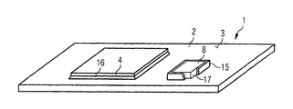
- FIG. 1 shows a semiconductor component including a substrate, to which a semiconductor chip and a passive device are fitted;
- FIG. 2 shows the passive device after being surrounded with a potting mold
- FIG. 3 shows the semiconductor component after the potting of the passive device and after the introduction of underfilling material between the semiconductor chip and the substrate.
- the semiconductor component 1 according to FIG. 1 includes a substrate 2 , for example, a rewiring substrate.
- a substrate 2 for example, a rewiring substrate.
- Arranged on the upper side 3 of the substrate 2 are at least one semiconductor chip 4 and at least one passive device 8 .
- the substrate 2 can also be populated with electronic components both on its upper side 3 and on its underside.
- the semiconductor chip 4 in FIG. 1 is designed using flip chip technology, but the use of other semiconductor chips is also conceivable.
- the semiconductor chip 4 includes on its active side 5 a number of flip chip contacts 6 (e.g., solder balls), which are soldered onto contact areas (not shown), on the substrate 2 and thus join the semiconductor chip 4 to the substrate 2 both electrically and mechanically.
- An interspace 7 is formed between the active side 5 of the semiconductor chip 4 and the upper side 3 of the substrate 2 .
- the passive device 8 (e.g., a resistor, a capacitor, coil or diode) has an underside 11 facing the substrate 2 , an upper side 9 and lateral sides 10 .
- the passive device 8 is fixed on the upper side 3 of the substrate 2 via soldered joints 12 and/or adhesive bonds (not shown).
- the passive device can also include a series of contacts 13 connecting the passive device electrically to the substrate 2 .
- An interspace 14 is also formed between the underside 11 of the passive device 8 and the upper side 3 of the substrate 2 .
- the passive device 8 has a height, h b .
- FIG. 1 shows the semiconductor component following the fitting of the semiconductor chip 4 and of the passive device 8 to the substrate 2 .
- the soldering process or reflow has been completed but no underfilling material has yet been applied.
- the intention is for the interspaces ( 7 , 14 ) to be filled, the underfilling material serving as a powerful adhesive layer between the substrate 2 and the semiconductor chip 4 and between the substrate 2 and the passive device 8 , and protects the soldered points in the event of alternating thermal loading.
- the passive device 8 is potted completely and not just underfilled to some extent.
- the passive device 8 is surrounded with a potting mold 15 , which is placed on the upper side 3 of the substrate 2 .
- the potting mold 15 has a height, h v , where h v should be at least as great as h b .
- the purpose of the potting mold is to permit the complete embedding of the passive device 8 with its underside 11 , its upper side 9 and its lateral sides 10 . Therefore, the potting mold 15 should be at least as high as the passive device 8 .
- the passive device 8 After the passive device 8 has been surrounded with the potting mold 15 , the passive device 8 can be potted.
- the passive device 8 it is possible to use the same plastic material utilized for the underfilling of the semiconductor chip 4 , or else a different plastic material, so that the application of the underfilling material and the potting can be carried out in a single process step.
- FIG. 3 shows the semiconductor component 1 after this process step.
- the interspace 7 between the semiconductor chip 4 and the surface 3 of the substrate 2 has been filled with an underfilling material 16 and the passive device has been potted with a plastic compound 17 . Therefore, in the event that the component is soldered to a system board, solder pumping effects are avoided.
Abstract
Description
Claims (7)
Priority Applications (1)
| Application Number | Priority Date | Filing Date | Title |
|---|---|---|---|
| US12/868,422 US8071433B2 (en) | 2006-05-12 | 2010-08-25 | Semiconductor component with surface mountable devices and method for producing the same |
Applications Claiming Priority (5)
| Application Number | Priority Date | Filing Date | Title |
|---|---|---|---|
| DE102006022748 | 2006-05-12 | ||
| DE102006022748.4A DE102006022748B4 (en) | 2006-05-12 | 2006-05-12 | Semiconductor device with surface mount devices and method of making the same |
| DE102006022748.4 | 2006-05-12 | ||
| US11/748,135 US7804178B2 (en) | 2006-05-12 | 2007-05-14 | Semiconductor component with surface mountable devices and method for producing the same |
| US12/868,422 US8071433B2 (en) | 2006-05-12 | 2010-08-25 | Semiconductor component with surface mountable devices and method for producing the same |
Related Parent Applications (1)
| Application Number | Title | Priority Date | Filing Date |
|---|---|---|---|
| US11/748,135 Division US7804178B2 (en) | 2006-05-12 | 2007-05-14 | Semiconductor component with surface mountable devices and method for producing the same |
Publications (2)
| Publication Number | Publication Date |
|---|---|
| US20100323479A1 US20100323479A1 (en) | 2010-12-23 |
| US8071433B2 true US8071433B2 (en) | 2011-12-06 |
Family
ID=38580136
Family Applications (2)
| Application Number | Title | Priority Date | Filing Date |
|---|---|---|---|
| US11/748,135 Expired - Fee Related US7804178B2 (en) | 2006-05-12 | 2007-05-14 | Semiconductor component with surface mountable devices and method for producing the same |
| US12/868,422 Expired - Fee Related US8071433B2 (en) | 2006-05-12 | 2010-08-25 | Semiconductor component with surface mountable devices and method for producing the same |
Family Applications Before (1)
| Application Number | Title | Priority Date | Filing Date |
|---|---|---|---|
| US11/748,135 Expired - Fee Related US7804178B2 (en) | 2006-05-12 | 2007-05-14 | Semiconductor component with surface mountable devices and method for producing the same |
Country Status (2)
| Country | Link |
|---|---|
| US (2) | US7804178B2 (en) |
| DE (1) | DE102006022748B4 (en) |
Citations (35)
| Publication number | Priority date | Publication date | Assignee | Title |
|---|---|---|---|---|
| US3585468A (en) * | 1968-11-27 | 1971-06-15 | Spraque Electric Co | Thermoplastic jacketed thermoplastic capacitor |
| US6018192A (en) * | 1998-07-30 | 2000-01-25 | Motorola, Inc. | Electronic device with a thermal control capability |
| US6108210A (en) | 1998-04-24 | 2000-08-22 | Amerasia International Technology, Inc. | Flip chip devices with flexible conductive adhesive |
| US6291267B1 (en) | 1999-06-09 | 2001-09-18 | International Business Machines Corporation | Process for underfilling chip-under-chip semiconductor modules |
| US6313521B1 (en) | 1998-11-04 | 2001-11-06 | Nec Corporation | Semiconductor device and method of manufacturing the same |
| US6351032B1 (en) * | 2000-01-20 | 2002-02-26 | National Semiconductor Corporation | Method and structure for heatspreader attachment in high thermal performance IC packages |
| US6392289B1 (en) | 1999-04-15 | 2002-05-21 | Micron Technology, Inc. | Integrated circuit substrate having through hole markings to indicate defective/non-defective status of same |
| US6407461B1 (en) * | 1997-06-27 | 2002-06-18 | International Business Machines Corporation | Injection molded integrated circuit chip assembly |
| US20020074669A1 (en) | 2000-12-15 | 2002-06-20 | Mitsubishi Denki Kabushiki Kaisha | Semiconductor device having capacitors for reducing power source noise |
| US20020108768A1 (en) | 2000-11-30 | 2002-08-15 | International Business Machines Corporation | I/C chip assembly and method of forming same |
| US20020140085A1 (en) | 2001-04-02 | 2002-10-03 | Lee Sang Ho | Semiconductor package including passive elements and method of manufacture |
| US20020173074A1 (en) | 2001-05-16 | 2002-11-21 | Walsin Advanced Electronics Ltd | Method for underfilling bonding gap between flip-chip and circuit substrate |
| US6546620B1 (en) | 2000-06-29 | 2003-04-15 | Amkor Technology, Inc. | Flip chip integrated circuit and passive chip component package fabrication method |
| US20030080437A1 (en) * | 2001-10-26 | 2003-05-01 | Intel Corporation | Electronic assembly with filled no-flow underfill and methods of manufacture |
| US6632704B2 (en) | 2000-12-19 | 2003-10-14 | Intel Corporation | Molded flip chip package |
| US20030201548A1 (en) * | 2000-09-25 | 2003-10-30 | Ryoichi Ikezawa | Epoxy resin molding material for sealing |
| US20040036162A1 (en) | 2002-08-21 | 2004-02-26 | Shih-Fang Chuang | Integrated circuit package with heatsink support |
| US20040113284A1 (en) | 2002-03-21 | 2004-06-17 | Broadcom Corporation | Method for making an enhanced die-up ball grid array package with two substrates |
| US20040180469A1 (en) * | 2002-05-13 | 2004-09-16 | Fortin Clement J. | SMT passive device noflow underfill methodology and structure |
| US20040227258A1 (en) * | 2003-05-14 | 2004-11-18 | Matsushita Electric Industrial Co., Ltd. | Electronic component packaging structure and method for producing the same |
| US20040240146A1 (en) * | 2003-05-27 | 2004-12-02 | Murata Manufacturing Co., Ltd. | Multilayer ceramic electronic component and mounting structure and method for the same |
| US20040262782A1 (en) | 2003-06-27 | 2004-12-30 | Ellis Thomas S. | Polymer encapsulated electrical devices |
| US20050017373A1 (en) * | 2003-06-06 | 2005-01-27 | Kazuhiro Nishikawa | Electronic circuit device and its manufacturing method |
| US6867486B2 (en) | 2001-08-30 | 2005-03-15 | Hynix Semiconductor Inc. | Stack chip module with electrical connection and adhesion of chips through a bump for improved heat release capacity |
| US6888259B2 (en) * | 2001-06-07 | 2005-05-03 | Denso Corporation | Potted hybrid integrated circuit |
| US20050121806A1 (en) * | 2003-12-04 | 2005-06-09 | White Electronic Designs Corporation | Method for attaching circuit elements |
| US6946601B1 (en) | 2004-05-28 | 2005-09-20 | Via Technologies Inc. | Electronic package with passive components |
| US7015591B2 (en) * | 2004-04-09 | 2006-03-21 | Airoha Technology Corp. | Exposed pad module integrating a passive device therein |
| US20060103030A1 (en) * | 2004-11-16 | 2006-05-18 | Makoto Aoki | Module substrate and disk apparatus |
| US20060158863A1 (en) * | 2005-01-19 | 2006-07-20 | Chi-Hsing Hsu | Interconnection structure through passive component |
| US7087455B2 (en) | 2003-01-29 | 2006-08-08 | Matsushita Electric Industrial Co., Ltd. | Semiconductor device and manufacturing method for the same |
| US7109524B2 (en) | 2003-05-06 | 2006-09-19 | Infineon Technologies Ag | Metal carrier (leadframe) for receiving and contact-connecting electrical and/or optoelectronic components |
| US20070087471A1 (en) | 2005-09-09 | 2007-04-19 | Advanced Semiconductor Engineering, Inc. | Semiconductor package and method of manufacturing the same |
| US7279771B2 (en) * | 2004-03-31 | 2007-10-09 | Shinko Electric Industries Co., Ltd. | Wiring board mounting a capacitor |
| US20080237890A1 (en) | 2004-05-21 | 2008-10-02 | Masamoto Tago | Semiconductor Device and Wiring Board |
-
2006
- 2006-05-12 DE DE102006022748.4A patent/DE102006022748B4/en not_active Expired - Fee Related
-
2007
- 2007-05-14 US US11/748,135 patent/US7804178B2/en not_active Expired - Fee Related
-
2010
- 2010-08-25 US US12/868,422 patent/US8071433B2/en not_active Expired - Fee Related
Patent Citations (36)
| Publication number | Priority date | Publication date | Assignee | Title |
|---|---|---|---|---|
| US3585468A (en) * | 1968-11-27 | 1971-06-15 | Spraque Electric Co | Thermoplastic jacketed thermoplastic capacitor |
| US6407461B1 (en) * | 1997-06-27 | 2002-06-18 | International Business Machines Corporation | Injection molded integrated circuit chip assembly |
| US6108210A (en) | 1998-04-24 | 2000-08-22 | Amerasia International Technology, Inc. | Flip chip devices with flexible conductive adhesive |
| US6018192A (en) * | 1998-07-30 | 2000-01-25 | Motorola, Inc. | Electronic device with a thermal control capability |
| US6313521B1 (en) | 1998-11-04 | 2001-11-06 | Nec Corporation | Semiconductor device and method of manufacturing the same |
| US6392289B1 (en) | 1999-04-15 | 2002-05-21 | Micron Technology, Inc. | Integrated circuit substrate having through hole markings to indicate defective/non-defective status of same |
| US6291267B1 (en) | 1999-06-09 | 2001-09-18 | International Business Machines Corporation | Process for underfilling chip-under-chip semiconductor modules |
| US6351032B1 (en) * | 2000-01-20 | 2002-02-26 | National Semiconductor Corporation | Method and structure for heatspreader attachment in high thermal performance IC packages |
| US6546620B1 (en) | 2000-06-29 | 2003-04-15 | Amkor Technology, Inc. | Flip chip integrated circuit and passive chip component package fabrication method |
| US20030201548A1 (en) * | 2000-09-25 | 2003-10-30 | Ryoichi Ikezawa | Epoxy resin molding material for sealing |
| US20020108768A1 (en) | 2000-11-30 | 2002-08-15 | International Business Machines Corporation | I/C chip assembly and method of forming same |
| US20020074669A1 (en) | 2000-12-15 | 2002-06-20 | Mitsubishi Denki Kabushiki Kaisha | Semiconductor device having capacitors for reducing power source noise |
| US6632704B2 (en) | 2000-12-19 | 2003-10-14 | Intel Corporation | Molded flip chip package |
| US20020140085A1 (en) | 2001-04-02 | 2002-10-03 | Lee Sang Ho | Semiconductor package including passive elements and method of manufacture |
| US20020173074A1 (en) | 2001-05-16 | 2002-11-21 | Walsin Advanced Electronics Ltd | Method for underfilling bonding gap between flip-chip and circuit substrate |
| US6888259B2 (en) * | 2001-06-07 | 2005-05-03 | Denso Corporation | Potted hybrid integrated circuit |
| US6867486B2 (en) | 2001-08-30 | 2005-03-15 | Hynix Semiconductor Inc. | Stack chip module with electrical connection and adhesion of chips through a bump for improved heat release capacity |
| US20030080437A1 (en) * | 2001-10-26 | 2003-05-01 | Intel Corporation | Electronic assembly with filled no-flow underfill and methods of manufacture |
| US20040113284A1 (en) | 2002-03-21 | 2004-06-17 | Broadcom Corporation | Method for making an enhanced die-up ball grid array package with two substrates |
| US20040180469A1 (en) * | 2002-05-13 | 2004-09-16 | Fortin Clement J. | SMT passive device noflow underfill methodology and structure |
| US7109592B2 (en) | 2002-05-13 | 2006-09-19 | International Business Machines Corporation | SMT passive device noflow underfill methodology and structure |
| US20040036162A1 (en) | 2002-08-21 | 2004-02-26 | Shih-Fang Chuang | Integrated circuit package with heatsink support |
| US7087455B2 (en) | 2003-01-29 | 2006-08-08 | Matsushita Electric Industrial Co., Ltd. | Semiconductor device and manufacturing method for the same |
| US7109524B2 (en) | 2003-05-06 | 2006-09-19 | Infineon Technologies Ag | Metal carrier (leadframe) for receiving and contact-connecting electrical and/or optoelectronic components |
| US20040227258A1 (en) * | 2003-05-14 | 2004-11-18 | Matsushita Electric Industrial Co., Ltd. | Electronic component packaging structure and method for producing the same |
| US20040240146A1 (en) * | 2003-05-27 | 2004-12-02 | Murata Manufacturing Co., Ltd. | Multilayer ceramic electronic component and mounting structure and method for the same |
| US20050017373A1 (en) * | 2003-06-06 | 2005-01-27 | Kazuhiro Nishikawa | Electronic circuit device and its manufacturing method |
| US20040262782A1 (en) | 2003-06-27 | 2004-12-30 | Ellis Thomas S. | Polymer encapsulated electrical devices |
| US20050121806A1 (en) * | 2003-12-04 | 2005-06-09 | White Electronic Designs Corporation | Method for attaching circuit elements |
| US7279771B2 (en) * | 2004-03-31 | 2007-10-09 | Shinko Electric Industries Co., Ltd. | Wiring board mounting a capacitor |
| US7015591B2 (en) * | 2004-04-09 | 2006-03-21 | Airoha Technology Corp. | Exposed pad module integrating a passive device therein |
| US20080237890A1 (en) | 2004-05-21 | 2008-10-02 | Masamoto Tago | Semiconductor Device and Wiring Board |
| US6946601B1 (en) | 2004-05-28 | 2005-09-20 | Via Technologies Inc. | Electronic package with passive components |
| US20060103030A1 (en) * | 2004-11-16 | 2006-05-18 | Makoto Aoki | Module substrate and disk apparatus |
| US20060158863A1 (en) * | 2005-01-19 | 2006-07-20 | Chi-Hsing Hsu | Interconnection structure through passive component |
| US20070087471A1 (en) | 2005-09-09 | 2007-04-19 | Advanced Semiconductor Engineering, Inc. | Semiconductor package and method of manufacturing the same |
Also Published As
| Publication number | Publication date |
|---|---|
| US20070262433A1 (en) | 2007-11-15 |
| DE102006022748B4 (en) | 2019-01-17 |
| US7804178B2 (en) | 2010-09-28 |
| DE102006022748A1 (en) | 2007-11-15 |
| US20100323479A1 (en) | 2010-12-23 |
Similar Documents
| Publication | Publication Date | Title |
|---|---|---|
| US10199312B1 (en) | Method of forming a packaged semiconductor device having enhanced wettable flank and structure | |
| JP4703556B2 (en) | Method of attaching flip chip to electrical substrate, flip chip assembly and method of forming underfill coated wafer | |
| JP4809761B2 (en) | Method for attaching area array device to electric substrate and patterned underfill film | |
| US6093972A (en) | Microelectronic package including a polymer encapsulated die | |
| US6835598B2 (en) | Stacked semiconductor module and method of manufacturing the same | |
| JP2002252303A (en) | Flip-chip semiconductor device for molded chip-scale package, and assembling method therefor | |
| US20060097404A1 (en) | Semiconductor package with conductive molding compound and manufacturing method thereof | |
| JP2004349495A (en) | Semiconductor device and its manufacturing method, and electronic device and electronic equipment | |
| US20080174978A1 (en) | Electronic component built-in substrate and method of manufacturing electronic component built-in substrate | |
| US20090051019A1 (en) | Multi-chip module package | |
| CN103915405B (en) | Semiconductor device and method of making a semiconductor device | |
| US7432601B2 (en) | Semiconductor package and fabrication process thereof | |
| US20080293189A1 (en) | Method of manufacturing chip integrated substrate | |
| US7439098B2 (en) | Semiconductor package for encapsulating multiple dies and method of manufacturing the same | |
| US6259155B1 (en) | Polymer enhanced column grid array | |
| US20030127720A1 (en) | Multi-chip stack package and fabricating method thereof | |
| JP2003059970A (en) | Electronic component-packaging structure and method therefor | |
| US5888849A (en) | Method for fabricating an electronic package | |
| US8071433B2 (en) | Semiconductor component with surface mountable devices and method for producing the same | |
| JP2004063516A (en) | Method of manufacturing semiconductor device | |
| US8268671B2 (en) | Semiconductor system-in-package and methods for making the same | |
| CN1173737A (en) | Method of packaging fragile devices with gel medium confined by rim member | |
| JP2004055609A (en) | Method of resin sealing | |
| US20060270109A1 (en) | Manufacturing method for an electronic component assembly and corresponding electronic component assembly | |
| TWI393197B (en) | Chip package |
Legal Events
| Date | Code | Title | Description |
|---|---|---|---|
| FEPP | Fee payment procedure |
Free format text: PAYOR NUMBER ASSIGNED (ORIGINAL EVENT CODE: ASPN); ENTITY STATUS OF PATENT OWNER: LARGE ENTITY |
|
| STCF | Information on status: patent grant |
Free format text: PATENTED CASE |
|
| FPAY | Fee payment |
Year of fee payment: 4 |
|
| FEPP | Fee payment procedure |
Free format text: MAINTENANCE FEE REMINDER MAILED (ORIGINAL EVENT CODE: REM.); ENTITY STATUS OF PATENT OWNER: LARGE ENTITY |
|
| LAPS | Lapse for failure to pay maintenance fees |
Free format text: PATENT EXPIRED FOR FAILURE TO PAY MAINTENANCE FEES (ORIGINAL EVENT CODE: EXP.); ENTITY STATUS OF PATENT OWNER: LARGE ENTITY |
|
| STCH | Information on status: patent discontinuation |
Free format text: PATENT EXPIRED DUE TO NONPAYMENT OF MAINTENANCE FEES UNDER 37 CFR 1.362 |
|
| FP | Lapsed due to failure to pay maintenance fee |
Effective date: 20191206 |