US8060453B2 - System and method for funds recovery from an integrated postal security device - Google Patents
System and method for funds recovery from an integrated postal security device Download PDFInfo
- Publication number
- US8060453B2 US8060453B2 US12/347,077 US34707708A US8060453B2 US 8060453 B2 US8060453 B2 US 8060453B2 US 34707708 A US34707708 A US 34707708A US 8060453 B2 US8060453 B2 US 8060453B2
- Authority
- US
- United States
- Prior art keywords
- postal security
- security device
- postal
- volatile memory
- registers
- Prior art date
- Legal status (The legal status is an assumption and is not a legal conclusion. Google has not performed a legal analysis and makes no representation as to the accuracy of the status listed.)
- Active, expires
Links
Images


Classifications
-
- G—PHYSICS
- G07—CHECKING-DEVICES
- G07B—TICKET-ISSUING APPARATUS; FARE-REGISTERING APPARATUS; FRANKING APPARATUS
- G07B17/00—Franking apparatus
- G07B17/00185—Details internally of apparatus in a franking system, e.g. franking machine at customer or apparatus at post office
-
- G—PHYSICS
- G07—CHECKING-DEVICES
- G07B—TICKET-ISSUING APPARATUS; FARE-REGISTERING APPARATUS; FRANKING APPARATUS
- G07B17/00—Franking apparatus
- G07B17/00016—Relations between apparatus, e.g. franking machine at customer or apparatus at post office, in a franking system
- G07B17/0008—Communication details outside or between apparatus
- G07B2017/00153—Communication details outside or between apparatus for sending information
- G07B2017/00169—Communication details outside or between apparatus for sending information from a franking apparatus, e.g. for verifying accounting
-
- G—PHYSICS
- G07—CHECKING-DEVICES
- G07B—TICKET-ISSUING APPARATUS; FARE-REGISTERING APPARATUS; FRANKING APPARATUS
- G07B17/00—Franking apparatus
- G07B17/00185—Details internally of apparatus in a franking system, e.g. franking machine at customer or apparatus at post office
- G07B17/00193—Constructional details of apparatus in a franking system
- G07B2017/00258—Electronic hardware aspects, e.g. type of circuits used
-
- G—PHYSICS
- G07—CHECKING-DEVICES
- G07B—TICKET-ISSUING APPARATUS; FARE-REGISTERING APPARATUS; FRANKING APPARATUS
- G07B17/00—Franking apparatus
- G07B17/00185—Details internally of apparatus in a franking system, e.g. franking machine at customer or apparatus at post office
- G07B17/00314—Communication within apparatus, personal computer [PC] system, or server, e.g. between printhead and central unit in a franking machine
- G07B2017/00338—Error detection or handling
-
- G—PHYSICS
- G07—CHECKING-DEVICES
- G07B—TICKET-ISSUING APPARATUS; FARE-REGISTERING APPARATUS; FRANKING APPARATUS
- G07B17/00—Franking apparatus
- G07B17/00185—Details internally of apparatus in a franking system, e.g. franking machine at customer or apparatus at post office
- G07B17/00362—Calculation or computing within apparatus, e.g. calculation of postage value
- G07B2017/00395—Memory organization
- G07B2017/00403—Memory zones protected from unauthorized reading or writing
Definitions
- the illustrative embodiments described in the present application relate generally to mailing machines including integrated circuits such as those used in postal security devices, and more particularly to systems and methods for recovering data such as postal funds records from a disabled integrated circuit in a postal security device.
- Mailing machines for printing postage indicia on envelopes and other forms of mail pieces have enjoyed considerable commercial success.
- There are many different types of mailing machines ranging from relatively small units that handle only one mail piece at a time, to large, multi-functional units that can process hundreds of mail pieces per hour in a continuous stream operation.
- Prior modern mailing machines that include postage meters store funds locally in an electronic postal security device (PSD).
- PSD electronic postal security device
- the postage fund credits are acquired through a postage purchase transaction known as a reset that is now typically electronically processed over a network connected to a data center.
- PSDs including multiple integrated circuit devices packaged in a physically secure housing.
- the PSD typically includes cryptographic data including key data stored in memory that are required for operation of the PSD device.
- the PSDs also include postal funds record data in registers including an ascending register and a descending register.
- the funds related data registers may also include one or more piece count bucket registers and a PSD and/or postage meter identification number.
- a PSD processor integrated circuit might fail, but the separate memory device might remain functioning and continue to store the funds record data. In such a scenario, the funds record memory device could be removed from the PSD circuit board and read.
- a secure housing is described for multiple circuit devices.
- an operating PSD was configured to visually output the funds register data in response to determining that the communications link to the postage metering device had failed. In that scenario, the PSD is operating normally, but the host postage meter has failed.
- Such a PSD is described in commonly-assigned U.S. Pat. No. 5,963,928 issued on Oct. 5, 1999 to Lee, entitled Secure Metering Vault Having LED Output for Recovery of Postal funds,” and incorporated herein by reference in its entirety.
- the present application describes illustrative embodiments of systems and methods for providing funds recovery for mailing machines including integrated circuits such as those used in postal security devices.
- the application more particularly describes systems and methods for recovering data such as postal funds records from a disabled integrated circuit in a postal security device.
- a postal security device comprises logic contained primarily in a single integrated circuit such as an application specific integrated circuit having a processor, memory, associated logic and a non-volatile memory for storing postal funds record data.
- the application specific integrated circuit also includes a special purpose state machine configured to provide an emergency read-only mode for access to the non-volatile memory if another section of the circuit should fail.
- the state machine and non-volatile memory have a secondary power circuit and a secondary clock circuit used to provide access to the non-volatile memory.
- the write enable function of the non-volatile memory is disabled if an emergency read function is initiated.
- the state machine enters the emergency read state by first erasing cryptographic keys in the postal security device in order to disable cryptographic processing in the device. Accordingly, the postal security device funds transactions functions are disabled if an emergency read function is performed on the postal funds record registers.
- a second JTAG port or multiplexed JTAG port is used to provide read-only access to a section of non-volatile memory storing postal funds record data.
- FIG. 1 is a schematic diagram of a mailing machine including an integrated circuit postal security device according to an illustrative embodiment of the present application.
- FIG. 2 is a partial schematic diagram of the mailing machine of FIG. 1 including a user interface controller including a postal security device and a printer subsystem including controller and media transport.
- FIG. 3 is a schematic diagram of a user interface controller and a connected postal security device according to an illustrative embodiment of the present application.
- FIG. 4 is a schematic diagram of a state machine of the postal security device of FIG. 3 .
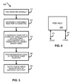
- FIG. 5 is a flow chart describing a process for reading postal security record registers in a partially disabled integrated postal security device according to an illustrative embodiment of the present application.
- FIG. 6 is a schematic diagram of a postal security device according to an illustrative embodiment of the present application.
- the illustrative embodiments of the present application describe systems and methods for providing funds recovery for mailing machines including integrated circuits such as those used in postal security devices, and more particularly to systems and methods for recovering data such as postal funds records from a disabled integrated circuit in a postal security device.
- PSDs postal security devices
- the processor, power distribution, clock or other subsystem of the module may fail.
- the memory device storing the postal funds data records may be removed from a dismantled PSD and read in order to retrieve the data.
- interconnection nodes since interconnection nodes are available, faulty components could be bypassed and other signal control utilized to read the relevant memory devices.
- the illustrative embodiments herein describe a highly integrated PSD such as one having many of its traditional processing elements housed in a single Application Specific Integrated Circuit (ASIC).
- ASIC Application Specific Integrated Circuit
- the embodiments provide for a secondary access subsystem to allow independent access to the postal funds data records using additional gates designed into the ASIC to allow access to the small number of bytes of memory that comprise the postal funds records such as the ascending register, descending register, piece count and meter identification number.
- the illustrative embodiments described herein relate to postage value transactions, but the teachings of the embodiments described may be applied to other value metering devices.
- a highly integrated PSD such as a PSD on a single chip
- NVM non-volatile memory
- access to the relevant NVM would be controlled by circuitry resident in the single integrated circuit. Accordingly, access to the postal data records may not be possible if the integrated ASIC fails in such a way as to prevent normal memory access such as through a processor read of the memory device.
- a highly integrated ASIC with multiple functions is more complex and includes more functionality and logic gates. Accordingly, such an ASIC is more likely to fail due to a problem with an unrelated part of the ASIC than would be likely with a multi-chip module. It has been found that a relatively small number of logic gates may be added to such an ASIC to greatly enhance the likelihood that relevant data might be retrieved from a partially failed ASIC using the systems and methods described herein.
- the mailing machine 10 comprises a base unit, designated generally by the reference numeral 12 , the base unit 12 includes a mail piece input end, designated generally by the reference numeral 14 and a mail piece output end, designated generally by the reference numeral 16 .
- One or more cover members 24 are pivotally mounted on the base 12 so as to move from the closed position shown in FIG. 1 to an open position (not shown) so as to expose various operating components and parts for service and/or repair as needed.
- the base unit 12 further includes a horizontal feed deck 30 , 36 , 38 which extends substantially from the input end 14 to the output end 16 .
- a plurality of nudger rollers 32 are suitably mounted under the feed deck 30 and project upwardly through openings in the feed deck so that the periphery of the rollers 32 is slightly above the upper surface of the feed deck 30 and can exert a forward feeding force on a succession of mail pieces placed in the input end 14 .
- a vertical wall 34 defines a mail piece stacking location from which the mail pieces are fed by the nudger rollers 32 along the feed deck 30 and into a transport subsystem that transports the media such as envelopes to be franked to the inkjet printing subsystem (not shown) that is generally located under cover 24 .
- a control unit 18 (user interface controller, UIC) is mounted on the base unit 12 , and includes one or more input/output devices, such as, for example, a keyboard 20 and a display device 22 .
- the control unit includes a main processor (not shown) and a postal security device (PSD) (not shown).
- mailing machine 10 comprises a modified version of the DM 500 mailing machine available from Pitney Bowes Inc. of Stamford Conn., wherein the mailing machine 10 is modified to include an integrated circuit postal security device as described herein.
- the postal security device is a secure value vault configured to store postage funds.
- FIG. 2 a partial schematic diagram of the mailing machine 10 of FIG. 1 including a user interface controller 18 including a postal security device 300 and a printer subsystem including controller and media transport is shown.
- the controller and transport subsystem configuration is illustrative and other suitable subsystem configurations may be substituted as appropriate.
- the mailing machine 10 includes an integrated ASIC based postal security device 300 as described more fully herein.
- the conveyor subsystem includes a singulator module 210 that receives a stack of media such as a stack of envelopes (not shown) including envelope 211 , or other mail pieces such as postcards, folders and the like, and separates and feeds them serially in a path of travel as indicated by arrow A.
- the conveyor subsystem feeds the envelopes 211 in the path of travel A along a deck past the printer subsystem so that a postal indicia or other marking can be printed on each envelope 211 .
- the singulator module 210 and the conveyor module make up a transport subsystem for feeding the media in mailing machine 10 .
- the singulator module 210 includes a feeder assembly 214 and a retard assembly 212 which work cooperatively to separate a stack of envelopes (not shown) and feed them one at a time to a pair of take-away rollers 216 .
- the feeder assembly 214 and take-away rollers are driven by motor M 1 using any suitable drive train (not shown).
- the conveyor subsystem includes an endless belt subsystem 218 including a belt and pulleys (including a drive pulley driven by motor M 2 ) mounted to any suitable structure (not shown) such as a frame.
- the drive pulley is operatively connected to motor M 2 by any conventional means such as intermeshing gears (not shown) or a timing belt (not shown) and controlled by motor controller 222 in order to advance the envelope 211 along the path of travel A.
- the conveyor subsystem also includes a plurality of idler pulleys with normal rollers 219 .
- the normal force rollers 219 work to bias the envelope 211 up against the deck including a top registration plate in a system known as top surface registration.
- the registration plate In the area of the print subsystem, the registration plate has appropriate opening and media “ski” 272 near the print head 260 used to top register the mail piece.
- the print head 260 is used to print cryptographically secure postal indicia that provide evidence of postage payment dispensed by postal security device 300 .
- the main controller subsystem 220 includes motor controller 222 , sensor controller 224 , and the print controller 228 along with associated memory and peripheral components (not shown) mounted on circuit boards in the mailing machine 10 chassis.
- the sensor controller 224 preferably controls media location detectors such as optical position detectors and other mailing machine sensors (not shown).
- the user interface controller 18 may be removable from the mailing machine 10 and includes a circuit assembly 390 with a main processor/user interface controller 380 and a physically secure postal security device module 300 . Other modules of the mailing machine 10 have not been shown for the sake of clarity.
- Processor/user interface 380 includes a communications subsystem (not shown) for connection to a remote data center such as by modem dial-up connection or through an ETHERNET network to connect remotely through a network such as the INTERNET.
- Many mailing machines including a postage meter are configured to allow remote reset or addition of funds such as by connecting to a remote data center for postage funds purchase transactions.
- U.S. Pat. No. 4,376,299 issued Mar. 8, 1983 to Rivest and U.S. Pat. No. 4,787,045 issued Nov. 22, 1988 to Storace, et al. described data centers for remote postage meter recharging.
- Systems describing secure PSDs are shown in commonly-owned U.S. Pat. No. 4,813,912, issued Mar. 21, 1989 to Chickneas, et al. and U.S. Pat. No. 5,812,990 issued Sep. 22, 1998 to Ryan, Jr., et al.
- FIG. 3 a schematic diagram of a user interface controller circuit 390 and a connected postal security device 300 according to an illustrative embodiment of the present application is shown.
- a PSD having a single integrated circuit ASIC fails, it is possible that the postal security funds record locations will not be accessible though the normal data channel.
- Providing a second memory read channel for an emergency read procedure greatly increases the likelihood that postal funds record data may be retrieved from a partially disabled ASIC. Removing the ASIC “die” from its package in order to probe internal pads or gates would be extremely difficult and costly as compared to access through a properly configured second channel.
- the postal funds data records are also known as Funds Relevant Data Items (FRDIs) and are typically stored in NVM memory in a PSD. Because a single, monolithic ASIC PSD is utilized here, the memory is difficult to access in a partial failure mode. In a multi-chip PSD module, a discrete memory device could be removed and individually powered and controlled in order to read postal funds data records after a PSD failure. A partial failure of the ASIC may involve the processor 320 or support circuitry and therefore, normal access to the memory storing FRDIs would not be possible.
- the NVM storing FRDIs is implemented as a parallel EEPROM, but has a virtual second read only port provided by the state machine 350 and multiplexing bus access to provide read only access to the relevant registers.
- a PSD typically includes Security Relevant Data Items (SRDIs) such as PKI and secret key system cryptographic keys.
- SRDIs Security Relevant Data Items
- the emergency read process preferably sequentially reads the FRDIs in a read only mode with write access to the relevant NVM disabled.
- the user interface controller device 18 is removable from the base 12 of mailing machine 10 .
- the user interface controller circuit board 390 that includes the user interface main processor 380 and peripheral devices such as I/O 384 and memory 382 .
- the I/O subsystem 384 includes interconnection circuits to communicate with the electronics 220 of the mailing machine base 12 , the PSD 300 , and networks such as a modem subsystem, ETHERNET subsystem and/or WI-FI subsystem to provide access to remote systems such as data centers through private networks or public networks such as the INTERNET.
- the main processor memory 382 includes a memory map that includes multiple types of memory devices and multiple integrated circuits with association bus and signal control circuitry to provide SRAM, Dynamic RAM (DRAM) and/or NVM including EEPROM, Flash or BSRAM devices.
- the PSD 300 is connected to the processor/user interface electronics through a 12 finger card edge connector 316 . Alternatively, other connection ports may be used.
- the PSD 300 is preferably a FIPS 104-2, level 3 rated physically secure device.
- the PSD 300 is enclosed and includes a circuit board 310 having a crystal 312 , a battery 314 and other related support components (not shown).
- PSD ASIC 301 is mounted on circuit board 310 and is preferably physically secure.
- the circuit board 310 also includes an emergency read port 318 that includes the required backup power 352 , clock and/or data lines 358 needed to perform the emergency read procedures described herein. Alternatively, some of the relevant emergency read signals such as data bus lines may reside on port 316 or on another port.
- one or more JTAG ports 370 are provided.
- the PSD ASIC 301 includes an embedded processor core 320 such as an ARM7 processor core.
- the memory map of the device includes multiple memory types such as SRAM, DRAM, and NVM such as EEPROM, Flash and/or BSRAM.
- the PSD 300 includes relevant support circuitry such as power conditioning and distribution, clock dividers and drivers, test access, main bus control and other relevant devices (not shown).
- the memory bus 322 is representative and allows multiple access to at least relevant portions of the address and data busses required such as through a second bus and bus arbitrator along line 356 from the bus circuitry of state machine 350 .
- PSD memory 330 is not to scale.
- PSD memory 330 includes the main program memory, working memory, status registers and data storage.
- PSD are used to store funds using known register types including an ascending register that counts up all of the funds ever processed by the PSD and a descending register that counts down as the current funds are dispensed through postage indicia printing transactions are processed. Similarly, a piece count tracks the number of indicia printed.
- PSD memory 332 is a region of NVM memory that contains the postal funds data registers for storing data including the ascending register, the descending register, the piece count and the meter identification code. Memory 332 is an actual or virtual dual port memory.
- bus arbitration and the state machine 350 provide for a second partial read only port into the memory.
- the funds related data registers may also include one or more piece count bucket registers and a PSD and/or postage meter identification number. In alternative configurations, detailed data regarding each transaction may also be stored in addition to the piece count data.
- the ASIC has a separate power plane P 2 that has separate power and ground pins on the emergency port 318 .
- This power plane P 2 powers only the required EEPROM, bus and state machine gates required to perform the emergency read functions described herein.
- only P 2 powers the state machine components that are not needed to be powered to avoid interfering with normal operation of the ASIC.
- the main power could alternatively power the whole device and P 2 may be injected as a backup power source for the limited gates and devices needed to accomplish the emergency read function.
- the ASIC includes circuitry to prevent back-powering of circuitry other than the EEPROM section and its associated state machine circuitry.
- the emergency read port 318 provides certain of the emergency read signals to PSD 301 through a header.
- state machine 350 has backup power P 2 , backup clock CLK 2 and a serial bus connected. It provides control write enable WE, read enable and clock CLK 2 to the memory over 354 .
- the WE line in 354 is used to disable write functions in the memory.
- the ASIC 301 is configured to have an automatic write enable disable feature 370 whereby presence of emergency read backup power supply P 2 352 drives a gate to disable the write enable on at least the section of memory that holds the postal funds data records.
- the PSD 300 may alternatively use a small programmed general purpose processor such as an 8 bit 8051 compatible core or other secondary memory access channel device.
- FIG. 4 a schematic diagram 400 of a state machine 350 of the postal security device 300 of FIG. 3 is shown.
- the emergency read state machine 350 depicted in diagram 400 comprises a relatively small number of gates of ASIC 301 and powers up in state 410 .
- state 410 the PSD 300 is operating normally and the state machine 350 does nothing except stay in its home state on path 405 .
- an emergency read initiation state change 415 occurs, such as by sensing presence of P 2 or other control signal on the emergency read port 358 or even a control signal on card finger port 316 , the state machine transitions on path 415 to state 420 .
- state 420 the state machine processes its pre-read protocol that includes at least disabling of the write capability of the memory registers to be read. Additional optional steps include holding the reset pin of the embedded CPU processor 320 , holding down the main clock signal 312 if appropriate in the particular design and erasing secure locations such as cryptographic key storage registers.
- state machine performs the emergency read.
- the necessary bus control is asserted to control the memory bus and the postal funds record registers are read and serially output over the I2C serial port provided for emergency read functions.
- the state machine includes at least the start address of the register range and can serially increment the address to process the known range of postal funds data registers.
- the state machine provides the bus control and address information required to read the relevant registers.
- the state machine optionally includes a buffer to hold the relevant register data while it is serially outputting that data on the I2C channel.
- the postal funds record registers are actual dual port devices and the state machine controls the second read only port to process the emergency read request.
- the state machine then terminates by staying in state 430 on path 435 .
- state 430 continuously outputs the register data until power P 2 is removed.
- step 510 the process starts with a normally operating PSD.
- portions of the PSD ASIC may fail such that the postal funds record data is not accessible through the normal USB communications channel of the device.
- the device may have an emergency read port connected such as through a ribbon cable connection from a test fixture to an emergency read header on the PSD circuit card 310 .
- step 520 the process determines if the emergency read port cable is connected such as by sensing the presence of power on pin P 2 or the other signals on the emergency read port.
- step 530 if the emergency read port is connected, the process performs any pre-emergency read requirements such as erasing any security data including any cryptographic keys, disabling the main PSD CPU core and disabling the memory write capability for at least the memory locations that are to be read.
- step 540 the process performs the emergency read of the postal funds registers.
- step 550 the process outputs the postal funds register data and may output the data on a serial or parallel bus.
- a standard I2C serial port is used by the emergency read state machine to output the register contents.
- the ASIC includes an IEEE standard JTAG subsystem.
- the ASIC includes a standard JTAG testing subsystem 610 with JTAG state machine and appropriate pins and registers.
- the ASIC includes two JTAG ports. The first JTAG port 610 is used to test the processor and the other circuitry of the processor. Because the illustrative embodiment is a single logic integrated circuit solution, the JTAG port is not connected in serial or parallel to other JTAG enabled integrated circuits under test.
- the first JTAG port is then disabled after the manufacturing test process applied to the ASIC.
- the second JTAG port 620 is connected to access the postal funds records EEPROM register locations with a specific JTAG test program designed to read only the postal funds records locations out on the second JTAG channel.
- the state machine therefore provides a second memory port into the EEPROM that provides for a serial output of the memory registers in serial fashion over the JTAG2 serial bus.
- the JTAG test program is designed to erase security data such as the stored cryptographic keys as a security precaution.
- the second JTAG port 620 is clocked by CLK 2 .
- the EEPROM memory comprises dual port NVM memory such as dual port EEPROM memory having a primary channel through the system bus and then a secondary read-only channel accessible through the state machine 350 using a second bus.
- the processes described herein are programmed in the appropriate assembler language for the CPU processor used such as the RENASAS SH series processors or the INTEL ATOM processors. Alternatively, the C or C++ programming language or other appropriate higher level language may be utilized to create the programs resident in memory 382 .
- the computing subsystem 390 comprises a single board computer such as a RENESAS SH series single board computer or an INTEL ATOM x86 single board computer with a USB interface to the PSD 300 using 12 finger card edge connector 316 .
- the emergency read channel includes an I2C serial port with clock and data pins optionally on the 12 finger card edge connector 316 or on a header used for the invasive emergency read process.
- the ASIC processor 320 includes an embedded processor IP core such as the commonly used ARM7 core.
- the processors run on real-time or other operating systems such as QNX, embedded LINUX or WINDOWS CE stored in memory 330 , 382 .
- any other programmable or otherwise customizable integrated circuit such as Field-programmable gate array (FPGA) may be used.
- Embedded memory 330 , 332 includes a combination of Static RAM (SRAM), EEPROM and Battery-backed SRAM (BSRAM).
- the state machine is always powered such as by being connected to P 1 or by P 2 being normally supplied.
- the EEPROM memory 332 is dual port with a second read only port.
- the state machine includes a normal operation state that acts to create a separate redundant copy of the postal funds data registers in another EEPROM memory location that is not addressable by CPU processor 320 .
- the secondary memory location utilizes a memory bus to connect to the state machine in parallel.
- a serial bus could be utilized if the speed were sufficient. Since the state machine is in essence a parallel processor, the redundant read/write will not impact system performance.
- the state machine then provides an output of the backup registers, the primary registers or both during an emergency read function.
- the state machine includes a secondary cryptographic engine that uses a relatively small cryptographic key to digitally sign the combination of the PSD ID, the ascending register and the descending register in order to securely store the emergency copy of the postal funds registers.
- P 2 comprises a voltage level that is lower than the primary power voltage level such as 1 ⁇ 2 core voltage, but sufficient to power the NVM and state machine in a read only process.
- the clocking circuit to the NVM 332 may be multiplexed such that the presence of P 2 selects CLK 2 for the memory device 332 .
- CLK 2 may alternatively be slower than CLK 1 such as 1 ⁇ 2 speed but sufficient to clock EEPROM 332 and state machine 350 in a read only mode.
- the ASIC core may typically run at anywhere from 10-300 Mhz as appropriate and at 1.8 V with 3.3 v and 5 v power available for other circuits.
- the PSD 300 comprises a primary single integrated circuit ASIC 301 including at least most of the logic functionality of the PSD.
- Ancillary circuits including minor integrated circuits may also be included on circuit board 310 in PSD 300 .
- Mail pieces as used herein may include a wide range of material such as postcards, letters, envelopes, flats and postal tape for application to a parcel.
Abstract
Description
Claims (16)
Priority Applications (2)
| Application Number | Priority Date | Filing Date | Title |
|---|---|---|---|
| US12/347,077 US8060453B2 (en) | 2008-12-31 | 2008-12-31 | System and method for funds recovery from an integrated postal security device |
| EP09015329.7A EP2204777B1 (en) | 2008-12-31 | 2009-12-10 | System and method for funds recovery from an integrated postal security device |
Applications Claiming Priority (1)
| Application Number | Priority Date | Filing Date | Title |
|---|---|---|---|
| US12/347,077 US8060453B2 (en) | 2008-12-31 | 2008-12-31 | System and method for funds recovery from an integrated postal security device |
Publications (2)
| Publication Number | Publication Date |
|---|---|
| US20100169240A1 US20100169240A1 (en) | 2010-07-01 |
| US8060453B2 true US8060453B2 (en) | 2011-11-15 |
Family
ID=42046335
Family Applications (1)
| Application Number | Title | Priority Date | Filing Date |
|---|---|---|---|
| US12/347,077 Active 2030-07-17 US8060453B2 (en) | 2008-12-31 | 2008-12-31 | System and method for funds recovery from an integrated postal security device |
Country Status (2)
| Country | Link |
|---|---|
| US (1) | US8060453B2 (en) |
| EP (1) | EP2204777B1 (en) |
Cited By (1)
| Publication number | Priority date | Publication date | Assignee | Title |
|---|---|---|---|---|
| US20110153910A1 (en) * | 2009-12-18 | 2011-06-23 | Mackenna Craig | Flash Memory-Interface |
Families Citing this family (2)
| Publication number | Priority date | Publication date | Assignee | Title |
|---|---|---|---|---|
| US8055936B2 (en) * | 2008-12-31 | 2011-11-08 | Pitney Bowes Inc. | System and method for data recovery in a disabled integrated circuit |
| JP2012108851A (en) * | 2010-11-19 | 2012-06-07 | Seiko Epson Corp | Control method for fiscal memory, and fiscal printer |
Citations (58)
| Publication number | Priority date | Publication date | Assignee | Title |
|---|---|---|---|---|
| US4253158A (en) | 1979-03-28 | 1981-02-24 | Pitney Bowes Inc. | System for securing postage printing transactions |
| US4310755A (en) | 1979-12-26 | 1982-01-12 | Pitney Bowes Inc. | Electronic postage meter radiant energy device circuit |
| US4376299A (en) | 1980-07-14 | 1983-03-08 | Pitney Bowes, Inc. | Data center for remote postage meter recharging system having physically secure encrypting apparatus and employing encrypted seed number signals |
| US4649266A (en) | 1984-03-12 | 1987-03-10 | Pitney Bowes Inc. | Method and apparatus for verifying postage |
| EP0302453A1 (en) | 1987-08-07 | 1989-02-08 | Siemens Nixdorf Informationssysteme Aktiengesellschaft | Data exchange system comprising user terminal and IC card |
| EP0328062A2 (en) | 1988-02-08 | 1989-08-16 | Pitney Bowes, Inc. | Fault tolerant smart card |
| US5111030A (en) | 1988-02-08 | 1992-05-05 | Pitney Bowes Inc. | Postal charge accounting system |
| US5400345A (en) | 1992-03-06 | 1995-03-21 | Pitney Bowes Inc. | Communications system to boundary-scan logic interface |
| WO1997006599A1 (en) | 1995-08-09 | 1997-02-20 | Xilinx, Inc. | Efficient in-system programming structure and method for non-volatile programmable logic devices |
| US5715431A (en) | 1993-04-13 | 1998-02-03 | Mondex International Limited | Tamper proof security measure in data writing to non-volatile memory |
| US5731980A (en) | 1996-08-23 | 1998-03-24 | Pitney Bowes Inc. | Electronic postage meter system having internal accounting system and removable external accounting system |
| US5749078A (en) | 1996-08-23 | 1998-05-05 | Pitney Bowes Inc. | Method and apparatus for storage of accounting information in a value dispensing system |
| US5774399A (en) | 1995-10-18 | 1998-06-30 | Hyundai Electronics Industries, Co., Ltd. | Flash memory device |
| US5793867A (en) | 1995-12-19 | 1998-08-11 | Pitney Bowes Inc. | System and method for disaster recovery in an open metering system |
| US5812990A (en) | 1996-12-23 | 1998-09-22 | Pitney Bowes Inc. | System and method for providing an additional cryptography layer for postage meter refills |
| US5841269A (en) | 1997-08-01 | 1998-11-24 | Pitney Bowes Inc. | Power-down circuit |
| US5938779A (en) | 1997-02-27 | 1999-08-17 | Alcatel Alsthom Compagnie Generale D'electricite | Asic control and data retrieval method and apparatus having an internal collateral test interface function |
| US5963928A (en) | 1997-07-17 | 1999-10-05 | Pitney Bowes Inc. | Secure metering vault having LED output for recovery of postal funds |
| US5978275A (en) | 1998-08-12 | 1999-11-02 | Nexflash, Technologies, Inc. | Erase and program control state machines for flash memory |
| US5999921A (en) | 1997-04-30 | 1999-12-07 | Pitney Bowes Inc. | Electronic postage meter system having plural clock system providing enhanced security |
| US6000774A (en) | 1998-03-24 | 1999-12-14 | Pitney Bowes Inc. | Mailing machine including ink jet operation checking for prevention of loss of postal funds |
| US6050486A (en) | 1996-08-23 | 2000-04-18 | Pitney Bowes Inc. | Electronic postage meter system separable printer and accounting arrangement incorporating partition of indicia and accounting information |
| US6061670A (en) | 1997-12-18 | 2000-05-09 | Pitney Bowes Inc. | Multiple registered postage meters |
| US6067262A (en) | 1998-12-11 | 2000-05-23 | Lsi Logic Corporation | Redundancy analysis for embedded memories with built-in self test and built-in self repair |
| US6085180A (en) | 1997-12-23 | 2000-07-04 | Pitney Bowes Inc. | Method and apparatus for controlling use of the downloading of graphical images from a portable device into a postage metering system |
| US6125162A (en) | 1998-08-20 | 2000-09-26 | Pitney Bowes Inc. | Postage meter having non-Gregorian calendar capability |
| US6141654A (en) | 1998-12-30 | 2000-10-31 | Pitney Bowes Inc. | Postage printing system having subsidized printing of third party messages |
| US6144950A (en) | 1998-02-27 | 2000-11-07 | Pitney Bowes Inc. | Postage printing system including prevention of tampering with print data sent from a postage meter to a printer |
| US6169804B1 (en) | 1996-11-21 | 2001-01-02 | Pitney Bowes Inc. | Method for verifying the expected postage security device and its status |
| US6175826B1 (en) | 1997-12-18 | 2001-01-16 | Pitney Bowes Inc. | Postage metering system and method for a stand-alone meter having virtual meter functionality |
| US6202057B1 (en) | 1997-12-18 | 2001-03-13 | Pitney Bowes Inc. | Postage metering system and method for a single vault dispensing postage to a plurality of printers |
| US6260144B1 (en) | 1996-11-21 | 2001-07-10 | Pitney Bowes Inc. | Method for verifying the expected postal security device in a postage metering system |
| US6295359B1 (en) | 1998-05-21 | 2001-09-25 | Pitney Bowes Inc. | Method and apparatus for distributing keys to secure devices such as a postage meter |
| US20020029348A1 (en) | 2000-07-28 | 2002-03-07 | Du Sterling D. | Smart card security information configuration and recovery system |
| US6397328B1 (en) | 1996-11-21 | 2002-05-28 | Pitney Bowes Inc. | Method for verifying the expected postage security device and an authorized host system |
| US6585433B2 (en) | 2001-03-09 | 2003-07-01 | Pitney Bowes Inc. | Print signal generation |
| US6591327B1 (en) | 1999-06-22 | 2003-07-08 | Silicon Storage Technology, Inc. | Flash memory with alterable erase sector size |
| US6592027B2 (en) | 2001-11-15 | 2003-07-15 | Pitney Bowes Inc. | Method for the recovery of unusable printed postage |
| US6629268B1 (en) | 2000-01-25 | 2003-09-30 | International Business Machines Corporation | Method and apparatus for servicing a processing system through a test port |
| US6839695B2 (en) | 2001-05-03 | 2005-01-04 | Pitney Bowes Inc. | Postage meter location system |
| US6868407B1 (en) | 2000-11-02 | 2005-03-15 | Pitney Bowes Inc. | Postage security device having cryptographic keys with a variable key length |
| US6928027B2 (en) | 2003-04-11 | 2005-08-09 | Qualcomm Inc | Virtual dual-port synchronous RAM architecture |
| US20050278499A1 (en) | 2004-06-09 | 2005-12-15 | David Durham | Cross validation of data using multiple subsystems |
| US20060013044A1 (en) | 2001-03-15 | 2006-01-19 | Paul Cheung | Programmable soft-start control for charge pump |
| US7143068B2 (en) | 2000-12-04 | 2006-11-28 | Pitney Bowes Inc. | Remote postage meter resetting system having rebate generating capabilities |
| US7194443B1 (en) | 1999-03-12 | 2007-03-20 | Francotyp-Postalia Ag & Co. | Method for protecting a security module and arrangement for the implementation of the method |
| US7233930B1 (en) | 2000-11-27 | 2007-06-19 | Pitney Bowes Inc. | Postage metering system including a printer having dual print heads |
| US20070165457A1 (en) | 2005-09-30 | 2007-07-19 | Jin-Ki Kim | Nonvolatile memory system |
| US7247791B2 (en) | 2004-05-27 | 2007-07-24 | Pitney Bowes Inc. | Security barrier for electronic circuitry |
| US7272581B2 (en) | 2002-03-12 | 2007-09-18 | Pitney Bowes Inc. | Method and system for optimizing throughput of mailing machines |
| US7293197B2 (en) * | 2003-08-13 | 2007-11-06 | Micro Memory Llc | Non-volatile memory with network fail-over |
| US7360068B2 (en) | 2003-01-31 | 2008-04-15 | Stmicroelectronics S.R.L. | Reconfigurable signal processing IC with an embedded flash memory device |
| US20080122484A1 (en) * | 2003-07-31 | 2008-05-29 | Actel Corporation | Integrated circuit device having state-saving and intitalization feature |
| US20080232174A1 (en) | 2007-03-14 | 2008-09-25 | Apple Inc. | Interleaving Charge Pumps for Programmable Memories |
| US20080253182A1 (en) | 2005-09-23 | 2008-10-16 | Samsung Electronics Co., Ltd. | Nand flash memory device and programming method |
| US20080298128A1 (en) | 2007-05-29 | 2008-12-04 | Samsung Electronics Co., Ltd. | Method of storing e-fuse data in flash memory device |
| US20090287602A1 (en) * | 2008-05-13 | 2009-11-19 | Neopost, Inc. | Method for postage payment |
| US20100165734A1 (en) | 2008-12-31 | 2010-07-01 | Sungwon Moh | System and method for data recovery in a disabled integrated circuit |
Family Cites Families (5)
| Publication number | Priority date | Publication date | Assignee | Title |
|---|---|---|---|---|
| US4421977A (en) | 1982-07-19 | 1983-12-20 | Pitney Bowes Inc. | Security system for electronic device |
| US4787045A (en) | 1986-04-10 | 1988-11-22 | Pitney Bowes Inc. | Postage meter recharging system |
| US4813912A (en) | 1986-09-02 | 1989-03-21 | Pitney Bowes Inc. | Secured printer for a value printing system |
| EP0598623B1 (en) | 1992-11-18 | 1997-05-21 | Pitney Bowes Inc. | Machine including apparatus for accounting for malfunction conditions |
| US6131090A (en) | 1997-03-04 | 2000-10-10 | Pitney Bowes Inc. | Method and system for providing controlled access to information stored on a portable recording medium |
-
2008
- 2008-12-31 US US12/347,077 patent/US8060453B2/en active Active
-
2009
- 2009-12-10 EP EP09015329.7A patent/EP2204777B1/en active Active
Patent Citations (60)
| Publication number | Priority date | Publication date | Assignee | Title |
|---|---|---|---|---|
| US4253158A (en) | 1979-03-28 | 1981-02-24 | Pitney Bowes Inc. | System for securing postage printing transactions |
| US4310755A (en) | 1979-12-26 | 1982-01-12 | Pitney Bowes Inc. | Electronic postage meter radiant energy device circuit |
| US4376299A (en) | 1980-07-14 | 1983-03-08 | Pitney Bowes, Inc. | Data center for remote postage meter recharging system having physically secure encrypting apparatus and employing encrypted seed number signals |
| US4649266A (en) | 1984-03-12 | 1987-03-10 | Pitney Bowes Inc. | Method and apparatus for verifying postage |
| EP0302453A1 (en) | 1987-08-07 | 1989-02-08 | Siemens Nixdorf Informationssysteme Aktiengesellschaft | Data exchange system comprising user terminal and IC card |
| US4908502A (en) | 1988-02-08 | 1990-03-13 | Pitney Bowes Inc. | Fault tolerant smart card |
| US5111030A (en) | 1988-02-08 | 1992-05-05 | Pitney Bowes Inc. | Postal charge accounting system |
| EP0328062B1 (en) | 1988-02-08 | 1994-04-20 | Pitney Bowes, Inc. | Fault tolerant smart card |
| EP0328062A2 (en) | 1988-02-08 | 1989-08-16 | Pitney Bowes, Inc. | Fault tolerant smart card |
| US5400345A (en) | 1992-03-06 | 1995-03-21 | Pitney Bowes Inc. | Communications system to boundary-scan logic interface |
| US5715431A (en) | 1993-04-13 | 1998-02-03 | Mondex International Limited | Tamper proof security measure in data writing to non-volatile memory |
| WO1997006599A1 (en) | 1995-08-09 | 1997-02-20 | Xilinx, Inc. | Efficient in-system programming structure and method for non-volatile programmable logic devices |
| US5774399A (en) | 1995-10-18 | 1998-06-30 | Hyundai Electronics Industries, Co., Ltd. | Flash memory device |
| US5793867A (en) | 1995-12-19 | 1998-08-11 | Pitney Bowes Inc. | System and method for disaster recovery in an open metering system |
| US5731980A (en) | 1996-08-23 | 1998-03-24 | Pitney Bowes Inc. | Electronic postage meter system having internal accounting system and removable external accounting system |
| US5749078A (en) | 1996-08-23 | 1998-05-05 | Pitney Bowes Inc. | Method and apparatus for storage of accounting information in a value dispensing system |
| US6050486A (en) | 1996-08-23 | 2000-04-18 | Pitney Bowes Inc. | Electronic postage meter system separable printer and accounting arrangement incorporating partition of indicia and accounting information |
| US6397328B1 (en) | 1996-11-21 | 2002-05-28 | Pitney Bowes Inc. | Method for verifying the expected postage security device and an authorized host system |
| US6260144B1 (en) | 1996-11-21 | 2001-07-10 | Pitney Bowes Inc. | Method for verifying the expected postal security device in a postage metering system |
| US6169804B1 (en) | 1996-11-21 | 2001-01-02 | Pitney Bowes Inc. | Method for verifying the expected postage security device and its status |
| US5812990A (en) | 1996-12-23 | 1998-09-22 | Pitney Bowes Inc. | System and method for providing an additional cryptography layer for postage meter refills |
| US5938779A (en) | 1997-02-27 | 1999-08-17 | Alcatel Alsthom Compagnie Generale D'electricite | Asic control and data retrieval method and apparatus having an internal collateral test interface function |
| US5999921A (en) | 1997-04-30 | 1999-12-07 | Pitney Bowes Inc. | Electronic postage meter system having plural clock system providing enhanced security |
| US5963928A (en) | 1997-07-17 | 1999-10-05 | Pitney Bowes Inc. | Secure metering vault having LED output for recovery of postal funds |
| US5841269A (en) | 1997-08-01 | 1998-11-24 | Pitney Bowes Inc. | Power-down circuit |
| US6175826B1 (en) | 1997-12-18 | 2001-01-16 | Pitney Bowes Inc. | Postage metering system and method for a stand-alone meter having virtual meter functionality |
| US6061670A (en) | 1997-12-18 | 2000-05-09 | Pitney Bowes Inc. | Multiple registered postage meters |
| US6202057B1 (en) | 1997-12-18 | 2001-03-13 | Pitney Bowes Inc. | Postage metering system and method for a single vault dispensing postage to a plurality of printers |
| US6085180A (en) | 1997-12-23 | 2000-07-04 | Pitney Bowes Inc. | Method and apparatus for controlling use of the downloading of graphical images from a portable device into a postage metering system |
| US6144950A (en) | 1998-02-27 | 2000-11-07 | Pitney Bowes Inc. | Postage printing system including prevention of tampering with print data sent from a postage meter to a printer |
| US6000774A (en) | 1998-03-24 | 1999-12-14 | Pitney Bowes Inc. | Mailing machine including ink jet operation checking for prevention of loss of postal funds |
| US6295359B1 (en) | 1998-05-21 | 2001-09-25 | Pitney Bowes Inc. | Method and apparatus for distributing keys to secure devices such as a postage meter |
| US5978275A (en) | 1998-08-12 | 1999-11-02 | Nexflash, Technologies, Inc. | Erase and program control state machines for flash memory |
| US6125162A (en) | 1998-08-20 | 2000-09-26 | Pitney Bowes Inc. | Postage meter having non-Gregorian calendar capability |
| US6067262A (en) | 1998-12-11 | 2000-05-23 | Lsi Logic Corporation | Redundancy analysis for embedded memories with built-in self test and built-in self repair |
| US6141654A (en) | 1998-12-30 | 2000-10-31 | Pitney Bowes Inc. | Postage printing system having subsidized printing of third party messages |
| US7194443B1 (en) | 1999-03-12 | 2007-03-20 | Francotyp-Postalia Ag & Co. | Method for protecting a security module and arrangement for the implementation of the method |
| US6591327B1 (en) | 1999-06-22 | 2003-07-08 | Silicon Storage Technology, Inc. | Flash memory with alterable erase sector size |
| US6629268B1 (en) | 2000-01-25 | 2003-09-30 | International Business Machines Corporation | Method and apparatus for servicing a processing system through a test port |
| US20020029348A1 (en) | 2000-07-28 | 2002-03-07 | Du Sterling D. | Smart card security information configuration and recovery system |
| US6868407B1 (en) | 2000-11-02 | 2005-03-15 | Pitney Bowes Inc. | Postage security device having cryptographic keys with a variable key length |
| US7233930B1 (en) | 2000-11-27 | 2007-06-19 | Pitney Bowes Inc. | Postage metering system including a printer having dual print heads |
| US7143068B2 (en) | 2000-12-04 | 2006-11-28 | Pitney Bowes Inc. | Remote postage meter resetting system having rebate generating capabilities |
| US6585433B2 (en) | 2001-03-09 | 2003-07-01 | Pitney Bowes Inc. | Print signal generation |
| US20060013044A1 (en) | 2001-03-15 | 2006-01-19 | Paul Cheung | Programmable soft-start control for charge pump |
| US6839695B2 (en) | 2001-05-03 | 2005-01-04 | Pitney Bowes Inc. | Postage meter location system |
| US6592027B2 (en) | 2001-11-15 | 2003-07-15 | Pitney Bowes Inc. | Method for the recovery of unusable printed postage |
| US7272581B2 (en) | 2002-03-12 | 2007-09-18 | Pitney Bowes Inc. | Method and system for optimizing throughput of mailing machines |
| US7360068B2 (en) | 2003-01-31 | 2008-04-15 | Stmicroelectronics S.R.L. | Reconfigurable signal processing IC with an embedded flash memory device |
| US6928027B2 (en) | 2003-04-11 | 2005-08-09 | Qualcomm Inc | Virtual dual-port synchronous RAM architecture |
| US20080122484A1 (en) * | 2003-07-31 | 2008-05-29 | Actel Corporation | Integrated circuit device having state-saving and intitalization feature |
| US7293197B2 (en) * | 2003-08-13 | 2007-11-06 | Micro Memory Llc | Non-volatile memory with network fail-over |
| US7247791B2 (en) | 2004-05-27 | 2007-07-24 | Pitney Bowes Inc. | Security barrier for electronic circuitry |
| US20050278499A1 (en) | 2004-06-09 | 2005-12-15 | David Durham | Cross validation of data using multiple subsystems |
| US20080253182A1 (en) | 2005-09-23 | 2008-10-16 | Samsung Electronics Co., Ltd. | Nand flash memory device and programming method |
| US20070165457A1 (en) | 2005-09-30 | 2007-07-19 | Jin-Ki Kim | Nonvolatile memory system |
| US20080232174A1 (en) | 2007-03-14 | 2008-09-25 | Apple Inc. | Interleaving Charge Pumps for Programmable Memories |
| US20080298128A1 (en) | 2007-05-29 | 2008-12-04 | Samsung Electronics Co., Ltd. | Method of storing e-fuse data in flash memory device |
| US20090287602A1 (en) * | 2008-05-13 | 2009-11-19 | Neopost, Inc. | Method for postage payment |
| US20100165734A1 (en) | 2008-12-31 | 2010-07-01 | Sungwon Moh | System and method for data recovery in a disabled integrated circuit |
Non-Patent Citations (2)
| Title |
|---|
| EPO Search Report in EP09015329.7-1229. |
| The European Search Report for European Patent Appplication No. 09015327.1. |
Cited By (2)
| Publication number | Priority date | Publication date | Assignee | Title |
|---|---|---|---|---|
| US20110153910A1 (en) * | 2009-12-18 | 2011-06-23 | Mackenna Craig | Flash Memory-Interface |
| US8266369B2 (en) * | 2009-12-18 | 2012-09-11 | Nxp B.V. | Flash memory interface |
Also Published As
| Publication number | Publication date |
|---|---|
| US20100169240A1 (en) | 2010-07-01 |
| EP2204777B1 (en) | 2017-09-20 |
| EP2204777A1 (en) | 2010-07-07 |
Similar Documents
| Publication | Publication Date | Title |
|---|---|---|
| US6050486A (en) | Electronic postage meter system separable printer and accounting arrangement incorporating partition of indicia and accounting information | |
| US3938095A (en) | Computer responsive postage meter | |
| EP0825561B1 (en) | Electronic postage meter system having internal accounting system and removable external accounting system | |
| GB2197257A (en) | A value printing system | |
| JPS63127393A (en) | Fare printing system for printing certificate stamp | |
| GB2174039A (en) | Postage and mailing information applying system | |
| US6502240B1 (en) | Digital postage meter system having a replaceable printing unit with system software upgrade | |
| US8060453B2 (en) | System and method for funds recovery from an integrated postal security device | |
| US6952777B1 (en) | Method for protecting a security module and arrangement for the implementation of the method | |
| US20070282764A1 (en) | Method and arrangement for backup of customer data stored in a franking machine | |
| US7882036B1 (en) | System and method for postal indicia printing evidencing and accounting | |
| US6954149B2 (en) | Method for protecting a security module and arrangement for the implementation of the method | |
| US4706215A (en) | Data protection system for electronic postage meters having multiple non-volatile multiple memories | |
| US4807141A (en) | Postage meter with microprocessor controlled reset inhibiting means | |
| US7305710B2 (en) | Method for securely loading and executing software in a secure device that cannot retain software after a loss of power | |
| US6362724B1 (en) | Security module and method for securing computerized postal registers against manipulation | |
| EP0657821A2 (en) | Memory monitoring circuit for detecting unauthorized memory access | |
| USRE31875E (en) | Computer responsive postage meter | |
| US6853986B1 (en) | Arrangement and method for generating a security imprint | |
| US6477512B1 (en) | Postage metering system having multiple postage meter configuration capability | |
| US5187798A (en) | Electronic postage meter having separate funds charge registers and recredits funds register in predetermined amount when funds fall to predetermined level | |
| US20050097066A1 (en) | Method and system for a mailing machine to verify the integrity of printed postage | |
| US8019696B2 (en) | Method and system to protect and track data from multiple meters on a removable storage medium | |
| US8510231B2 (en) | Method and system for printing multiple regions across a mail piece | |
| AU750360B2 (en) | Postage printing system having secure reporting of printer errors |
Legal Events
| Date | Code | Title | Description |
|---|---|---|---|
| AS | Assignment |
Owner name: PITNEY BOWES INC.,CONNECTICUT Free format text: ASSIGNMENT OF ASSIGNORS INTEREST;ASSIGNORS:TOLMIE, ROBERT J., JR.;CLARK, DOUGLAS A.;SCRIBE, MARK A.;SIGNING DATES FROM 20090127 TO 20090217;REEL/FRAME:022271/0491 Owner name: PITNEY BOWES INC., CONNECTICUT Free format text: ASSIGNMENT OF ASSIGNORS INTEREST;ASSIGNORS:TOLMIE, ROBERT J., JR.;CLARK, DOUGLAS A.;SCRIBE, MARK A.;SIGNING DATES FROM 20090127 TO 20090217;REEL/FRAME:022271/0491 |
|
| STCF | Information on status: patent grant |
Free format text: PATENTED CASE |
|
| FPAY | Fee payment |
Year of fee payment: 4 |
|
| MAFP | Maintenance fee payment |
Free format text: PAYMENT OF MAINTENANCE FEE, 8TH YEAR, LARGE ENTITY (ORIGINAL EVENT CODE: M1552); ENTITY STATUS OF PATENT OWNER: LARGE ENTITY Year of fee payment: 8 |
|
| AS | Assignment |
Owner name: JPMORGAN CHASE BANK, N.A., AS ADMINISTRATIVE AGENT Free format text: SECURITY INTEREST;ASSIGNORS:PITNEY BOWES INC.;NEWGISTICS, INC.;BORDERFREE, INC.;AND OTHERS;REEL/FRAME:050905/0640 Effective date: 20191101 Owner name: JPMORGAN CHASE BANK, N.A., AS ADMINISTRATIVE AGENT, NEW YORK Free format text: SECURITY INTEREST;ASSIGNORS:PITNEY BOWES INC.;NEWGISTICS, INC.;BORDERFREE, INC.;AND OTHERS;REEL/FRAME:050905/0640 Effective date: 20191101 |
|
| MAFP | Maintenance fee payment |
Free format text: PAYMENT OF MAINTENANCE FEE, 12TH YEAR, LARGE ENTITY (ORIGINAL EVENT CODE: M1553); ENTITY STATUS OF PATENT OWNER: LARGE ENTITY Year of fee payment: 12 |
|
| AS | Assignment |
Owner name: ALTER DOMUS (US) LLC, ILLINOIS Free format text: SECURITY INTEREST;ASSIGNORS:PITNEY BOWES, INC.;PITNEY BOWES GLOBAL LOGISTICS LLC;REEL/FRAME:064444/0313 Effective date: 20230731 |