US8058221B2 - Composition for removing a photoresist and method of manufacturing semiconductor device using the composition - Google Patents
Composition for removing a photoresist and method of manufacturing semiconductor device using the composition Download PDFInfo
- Publication number
- US8058221B2 US8058221B2 US13/080,763 US201113080763A US8058221B2 US 8058221 B2 US8058221 B2 US 8058221B2 US 201113080763 A US201113080763 A US 201113080763A US 8058221 B2 US8058221 B2 US 8058221B2
- Authority
- US
- United States
- Prior art keywords
- composition
- photoresist
- methyl
- amine
- comparative
- Prior art date
- Legal status (The legal status is an assumption and is not a legal conclusion. Google has not performed a legal analysis and makes no representation as to the accuracy of the status listed.)
- Active
Links
- 229920002120 photoresistant polymer Polymers 0.000 title claims abstract description 87
- 239000000203 mixture Substances 0.000 title claims abstract description 49
- 239000004065 semiconductor Substances 0.000 title abstract description 16
- 238000004519 manufacturing process Methods 0.000 title abstract description 14
- IAZDPXIOMUYVGZ-UHFFFAOYSA-N Dimethylsulphoxide Chemical compound CS(C)=O IAZDPXIOMUYVGZ-UHFFFAOYSA-N 0.000 claims abstract description 48
- 150000001412 amines Chemical class 0.000 claims abstract description 23
- 125000002887 hydroxy group Chemical group [H]O* 0.000 claims abstract description 19
- 125000002768 hydroxyalkyl group Chemical group 0.000 claims abstract description 10
- 239000003495 polar organic solvent Substances 0.000 claims abstract description 10
- WGTYBPLFGIVFAS-UHFFFAOYSA-M tetramethylammonium hydroxide Chemical group [OH-].C[N+](C)(C)C WGTYBPLFGIVFAS-UHFFFAOYSA-M 0.000 claims description 38
- ATHHXGZTWNVVOU-UHFFFAOYSA-N N-methylformamide Chemical compound CNC=O ATHHXGZTWNVVOU-UHFFFAOYSA-N 0.000 claims description 12
- VKYKSIONXSXAKP-UHFFFAOYSA-N hexamethylenetetramine Chemical compound C1N(C2)CN3CN1CN2C3 VKYKSIONXSXAKP-UHFFFAOYSA-N 0.000 claims description 11
- RPNUMPOLZDHAAY-UHFFFAOYSA-N Diethylenetriamine Chemical compound NCCNCCN RPNUMPOLZDHAAY-UHFFFAOYSA-N 0.000 claims description 9
- 235000010299 hexamethylene tetramine Nutrition 0.000 claims description 9
- 239000004312 hexamethylene tetramine Substances 0.000 claims description 9
- XLYOFNOQVPJJNP-UHFFFAOYSA-N water Substances O XLYOFNOQVPJJNP-UHFFFAOYSA-N 0.000 claims description 9
- QUSNBJAOOMFDIB-UHFFFAOYSA-N Ethylamine Chemical compound CCN QUSNBJAOOMFDIB-UHFFFAOYSA-N 0.000 claims description 8
- PIICEJLVQHRZGT-UHFFFAOYSA-N Ethylenediamine Chemical compound NCCN PIICEJLVQHRZGT-UHFFFAOYSA-N 0.000 claims description 8
- JGFZNNIVVJXRND-UHFFFAOYSA-N N,N-Diisopropylethylamine (DIPEA) Chemical compound CCN(C(C)C)C(C)C JGFZNNIVVJXRND-UHFFFAOYSA-N 0.000 claims description 8
- DJEQZVQFEPKLOY-UHFFFAOYSA-N N,N-dimethylbutylamine Chemical compound CCCCN(C)C DJEQZVQFEPKLOY-UHFFFAOYSA-N 0.000 claims description 7
- JJWLVOIRVHMVIS-UHFFFAOYSA-N isopropylamine Chemical compound CC(C)N JJWLVOIRVHMVIS-UHFFFAOYSA-N 0.000 claims description 7
- 125000002496 methyl group Chemical group [H]C([H])([H])* 0.000 claims description 4
- OKTJSMMVPCPJKN-UHFFFAOYSA-N Carbon Chemical compound [C] OKTJSMMVPCPJKN-UHFFFAOYSA-N 0.000 claims description 3
- FXHOOIRPVKKKFG-UHFFFAOYSA-N N,N-Dimethylacetamide Chemical compound CN(C)C(C)=O FXHOOIRPVKKKFG-UHFFFAOYSA-N 0.000 claims description 3
- 125000003282 alkyl amino group Chemical group 0.000 claims description 3
- 125000000217 alkyl group Chemical group 0.000 claims description 3
- 229910052799 carbon Inorganic materials 0.000 claims description 3
- 150000005622 tetraalkylammonium hydroxides Chemical group 0.000 claims description 3
- 230000000052 comparative effect Effects 0.000 description 37
- 239000010410 layer Substances 0.000 description 37
- 238000000034 method Methods 0.000 description 33
- 229910052802 copper Inorganic materials 0.000 description 21
- 239000010949 copper Substances 0.000 description 21
- RYGMFSIKBFXOCR-UHFFFAOYSA-N Copper Chemical compound [Cu] RYGMFSIKBFXOCR-UHFFFAOYSA-N 0.000 description 20
- 238000005530 etching Methods 0.000 description 19
- 238000007747 plating Methods 0.000 description 18
- 230000008014 freezing Effects 0.000 description 14
- 238000007710 freezing Methods 0.000 description 14
- 235000012431 wafers Nutrition 0.000 description 11
- 238000012360 testing method Methods 0.000 description 9
- 238000002161 passivation Methods 0.000 description 8
- 239000000758 substrate Substances 0.000 description 8
- 239000011229 interlayer Substances 0.000 description 7
- 238000002474 experimental method Methods 0.000 description 6
- 230000004888 barrier function Effects 0.000 description 5
- 238000005260 corrosion Methods 0.000 description 5
- 230000007797 corrosion Effects 0.000 description 5
- 238000000635 electron micrograph Methods 0.000 description 5
- XNWFRZJHXBZDAG-UHFFFAOYSA-N 2-METHOXYETHANOL Chemical compound COCCO XNWFRZJHXBZDAG-UHFFFAOYSA-N 0.000 description 4
- 239000002184 metal Substances 0.000 description 4
- 229910052751 metal Inorganic materials 0.000 description 4
- 239000002904 solvent Substances 0.000 description 4
- OKKJLVBELUTLKV-UHFFFAOYSA-N Methanol Chemical compound OC OKKJLVBELUTLKV-UHFFFAOYSA-N 0.000 description 3
- HXMVNCMPQGPRLN-UHFFFAOYSA-N 2-hydroxyputrescine Chemical compound NCCC(O)CN HXMVNCMPQGPRLN-UHFFFAOYSA-N 0.000 description 2
- ARSRBNBHOADGJU-UHFFFAOYSA-N 7,12-dimethyltetraphene Chemical compound C1=CC2=CC=CC=C2C2=C1C(C)=C(C=CC=C1)C1=C2C ARSRBNBHOADGJU-UHFFFAOYSA-N 0.000 description 2
- VFZRZRDOXPRTSC-UHFFFAOYSA-N DMBA Natural products COC1=CC(OC)=CC(C=O)=C1 VFZRZRDOXPRTSC-UHFFFAOYSA-N 0.000 description 2
- PXHVJJICTQNCMI-UHFFFAOYSA-N Nickel Chemical compound [Ni] PXHVJJICTQNCMI-UHFFFAOYSA-N 0.000 description 2
- LHIJANUOQQMGNT-UHFFFAOYSA-N aminoethylethanolamine Chemical compound NCCNCCO LHIJANUOQQMGNT-UHFFFAOYSA-N 0.000 description 2
- 239000003431 cross linking reagent Substances 0.000 description 2
- 229940028356 diethylene glycol monobutyl ether Drugs 0.000 description 2
- 230000002349 favourable effect Effects 0.000 description 2
- -1 for example Chemical class 0.000 description 2
- 238000005468 ion implantation Methods 0.000 description 2
- JCGNDDUYTRNOFT-UHFFFAOYSA-N oxolane-2,4-dione Chemical compound O=C1COC(=O)C1 JCGNDDUYTRNOFT-UHFFFAOYSA-N 0.000 description 2
- 239000000126 substance Substances 0.000 description 2
- NIXOWILDQLNWCW-UHFFFAOYSA-M Acrylate Chemical compound [O-]C(=O)C=C NIXOWILDQLNWCW-UHFFFAOYSA-M 0.000 description 1
- 241001424392 Lucia limbaria Species 0.000 description 1
- 150000003973 alkyl amines Chemical class 0.000 description 1
- 125000000118 dimethyl group Chemical group [H]C([H])([H])* 0.000 description 1
- 238000011156 evaluation Methods 0.000 description 1
- AVXURJPOCDRRFD-UHFFFAOYSA-N hydroxylamine group Chemical group NO AVXURJPOCDRRFD-UHFFFAOYSA-N 0.000 description 1
- 238000005259 measurement Methods 0.000 description 1
- 238000012986 modification Methods 0.000 description 1
- 230000004048 modification Effects 0.000 description 1
- 229910052759 nickel Inorganic materials 0.000 description 1
- 229920003986 novolac Polymers 0.000 description 1
- 230000003287 optical effect Effects 0.000 description 1
- 238000000059 patterning Methods 0.000 description 1
- 229920000642 polymer Polymers 0.000 description 1
- 239000000523 sample Substances 0.000 description 1
- 238000005507 spraying Methods 0.000 description 1
- 238000003860 storage Methods 0.000 description 1
- 150000003462 sulfoxides Chemical class 0.000 description 1
- 238000010257 thawing Methods 0.000 description 1
- 229910021642 ultra pure water Inorganic materials 0.000 description 1
- 239000012498 ultrapure water Substances 0.000 description 1
Images


Classifications
-
- G—PHYSICS
- G03—PHOTOGRAPHY; CINEMATOGRAPHY; ANALOGOUS TECHNIQUES USING WAVES OTHER THAN OPTICAL WAVES; ELECTROGRAPHY; HOLOGRAPHY
- G03F—PHOTOMECHANICAL PRODUCTION OF TEXTURED OR PATTERNED SURFACES, e.g. FOR PRINTING, FOR PROCESSING OF SEMICONDUCTOR DEVICES; MATERIALS THEREFOR; ORIGINALS THEREFOR; APPARATUS SPECIALLY ADAPTED THEREFOR
- G03F7/00—Photomechanical, e.g. photolithographic, production of textured or patterned surfaces, e.g. printing surfaces; Materials therefor, e.g. comprising photoresists; Apparatus specially adapted therefor
- G03F7/26—Processing photosensitive materials; Apparatus therefor
- G03F7/42—Stripping or agents therefor
- G03F7/422—Stripping or agents therefor using liquids only
- G03F7/425—Stripping or agents therefor using liquids only containing mineral alkaline compounds; containing organic basic compounds, e.g. quaternary ammonium compounds; containing heterocyclic basic compounds containing nitrogen
-
- C11D2111/22—
Definitions
- the present disclosure herein relates to a composition for removing a photoresist and a method of manufacturing a semiconductor device using the composition.
- a photoresist pattern may be used for various masks in, for example, an etching process, ion implantation process, and plating processes during a manufacturing process of a semiconductor device.
- a photoresist pattern should have excellent adhesion to the layer below, and may require chemical stability against etchants, plating solutions, etc.
- photoresist patterns are being made to have increasingly greater mechanical strength. After a photoresist pattern is used to perform, for example, an etching process, an ion-implantation process, a plating process, a process for removing the photoresist pattern may then be required.
- compositions for removing a photoresist which can readily remove a photoresist pattern while minimizing the corrosion of a metal layer and for a method of manufacturing a semiconductor device using the composition.
- the present disclosure may provide a composition for removing a photoresist, which can readily remove a photoresist pattern while minimizing the corrosion of a metal layer.
- the present disclosure may also provide a method of manufacturing a semiconductor device having improved reliability.
- Embodiments of the inventive concept provide a composition for removing a photoresist, including: about 60-90 wt % of dimethyl sulfoxide, about 10-30 wt % of a polar organic solvent, about 0.5-1.5 wt % of hydroxy alkyl ammonium and about 1-10 wt % of an amine containing no hydroxyl group.
- the polar organic solvent may be at least one selected from the group consisting of N-methyl-2-pyrolidione (NMP), N-methyl-formamide and dimethylacetamide.
- the hydroxy alkyl ammonium may be tetraalkyl ammonium hydroxide containing an alkyl group with a carbon number of about 1-4.
- the amine containing no hydroxyl group may be at least one selected from the alkyl amine group consisting of ethylamine, iso-propylamine, diethylenetriamine and ethylenediamine, hexamine, (2-dimethylamine)(methyl)amine, diisopropylethylamine and dimethylbutylamine.
- the composition for removing a photoresist may further include less than about 1.0 wt % of water.
- a composition for removing a photoresist includes: about 70-75 wt % of dimethyl sulfoxide, about 15-25 wt % of N-methyl-2-pyrolidione (NMP), about 0.70-1.50 wt % of tetramethylammonium hydroxide and about 1.5-5.0 wt % of amine containing no hydroxyl group.
- NMP N-methyl-2-pyrolidione
- a method of manufacturing a semiconductor device includes: forming a photoresist pattern on a substrate and removing the photoresist pattern using a composition for removing a photoresist.
- the composition for removing the photoresist includes about 60-90 wt % of dimethyl sulfoxide, about 10-30 wt % of a polar organic solvent, about 0.5-1.5 wt % of hydroxy alkyl ammonium and about 1-10 wt % of an amine containing no hydroxyl group.
- the removing of the photoresist pattern may be performed at a temperature of about 20-70° C.
- a method of manufacturing a semiconductor device includes forming an interlayer dielectric on a semiconductor substrate, forming a conductive pad on the interlayer dielectric, sequentially forming a first passivation layer and a second passivation layer covering a portion of the interlayer dielectric and exposing a portion of the conductive pad.
- the method further includes conformally forming a seed layer on substantially the entire surface of the semiconductor substrate on which the first passivation layer and the second passivation layer are formed, forming a photoresist pattern on the seed layer. The photoresist pattern exposes a portion of the seed layer overlapping with the conductive pad.
- the method further includes forming a barrier layer using a first plating process on a portion of the seed layer which is not covered with the photoresist pattern, forming a bump using a second plating process on the barrier layer and protruding above an upper surface of the photoresist pattern and removing the photoresist pattern using a composition for removing a photoresist.
- the composition for removing the photoresist includes about 70-75 wt % of dimethyl sulfoxide, about 15-25 wt % of N-methyl-2-pyrolidione (NMP), about 0.70-1.50 wt % of tetramethylammonium hydroxide and about 1.5-5.0 wt % of an amine containing no hydroxyl group.
- FIGS. 1 through 3 are cross-sectional views illustrating a method of manufacturing a semiconductor device according to an exemplary embodiment of the inventive concept
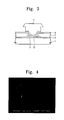
- FIG. 4 is an electron micrograph taken after removing a negative-type photoresist using the composition solution corresponding to an exemplary embodiment
- FIG. 5 is an electron micrograph taken after removing a negative-type photoresist using the solution corresponding to Comparative Example 3.
- FIG. 6 is an electron micrograph taken after removing a negative-type photoresist using the solution corresponding to Comparative Example 9.
- FIGS. 1 through 3 are cross-sectional views illustrating a method of manufacturing a semiconductor device according to an embodiment of the inventive concept.
- an interlayer dielectric 1 is stacked on a semiconductor substrate (not illustrated), and a conductive pad 3 is formed on the interlayer dielectric 1 .
- transistors and interconnections covered with the interlayer dielectric 1 may be formed on the semiconductor substrate.
- a first passivation layer 5 and a second passivation layer 7 which cover the interlayer dielectric 1 while exposing a portion of the conductive pad 3 , are formed.
- a seed layer 9 is conformally formed on the entire surface of the semiconductor substrate on which the first and the second passivation layers 5 and 7 are disposed.
- the seed layer 9 for example, may be formed of a copper-containing layer.
- a photoresist pattern 11 is formed on the seed layer 9 .
- the photoresist pattern 11 is formed to expose the seed layer overlapping with the conductive pad 3 .
- the photoresist pattern 11 may be a positive-type and a negative-type, but may be the negative-type for applying a subsequent high-speed plating method.
- the negative-type photoresist may contain a crosslinking agent, and polymers in a light-exposed portion may be crosslinked by the crosslinking agent such that the light-exposed portions change to an insoluble chemical state in a developing solution.
- the negative-type photoresist may have greater mechanical strength than a positive-type photoresist.
- a barrier layer 13 is formed using a first plating process on the seed layer 9 which is not covered with the photoresist pattern 11 .
- the barrier layer 13 may be formed of, for example, a nickel-containing layer.
- a bump 15 which fills the gap between the photoresist patterns 11 , may be formed on the barrier layer 13 .
- the bump 15 may be formed to protrude above the upper surface of the photoresist pattern 11 .
- the second plating process may be performed using, for example, a high-speed plating method.
- the temperature of a plating solution may be the same as that of a general plating method, but the current density applied to an electrode may be higher, and the high-speed plating method may be performed under a high concentration state of the plating solution.
- the photoresist pattern 11 is removed using a composition for removing a photoresist.
- the composition for removing a photoresist contains about 60-90 wt % of dimethyl sulfoxide, about 10-30 wt % of a polar organic solvent, about 0.5-1.5 wt % of hydroxy alkyl ammonium and about 1-10 wt % of an amine containing no hydroxyl group.
- the polar organic solvent may be at least one selected from the group consisting of, for example, N-methyl-2-pyrolidione (NMP), N-methyl-formamide and dimethylacetamide.
- the hydroxy alkyl ammonium may be, for example, tetraalkyl ammonium hydroxide containing an alkyl group with a carbon number of about 1-4.
- the amine containing no hydroxyl group may be, for example, at least one selected from the group consisting of ethylamine, iso-propylamine, diethylenetriamine and ethylenediamine, hexamine, (2-dimethylamine)(methyl)amine, diisopropylethylamine and dimethylbutylamine.
- the composition for removing a photoresist may further include less than about 1.0 wt % of water.
- the composition for removing a photoresist may include about 70-75 wt % of dimethyl sulfoxide; about 15-25 wt % of N-methyl-2-pyrolidione (NMP); about 0.7-1.50 wt % of tetramethylammonium hydroxide; and about 1.5-5.0 wt % of an amine containing no hydroxyl group.
- the seed layer 9 at the side of the bump 15 may be selectively removed to expose the upper surface of the second passivation layer 7 .
- composition solutions for removing a photoresist having 15 compositions (Embodiments 1-5 and Comparative Examples 1-10) described in Table 1 were manufactured.
- a copper layer was formed as a seed layer 9 on the entire surface of a wafer as in FIG. 1 .
- a positive-type novolac-based photoresist is coated to a thickness of about 40 ⁇ m, and a photoresist pattern 11 was formed by performing a photolithographic process.
- a bump 15 consisting of copper was formed by performing a plating process as in FIG. 2 .
- the first test wafer including the positive-type photoresist pattern 11 was formed in 15 pieces under the same process conditions.
- a copper layer was formed as a seed layer 9 on the entire surface of a wafer as in FIG. 1 .
- a negative-type acrylate-based photoresist is coated to a thickness of about 40 ⁇ m, and a photoresist pattern 11 was formed by performing a photolithographic process.
- a bump 15 consisting of copper was formed by performing a plating process as in FIG. 2 .
- the second test wafer including the negative-type photoresist pattern 11 was formed in 15 pieces under the same process conditions.
- Table 2 represents the results of product workability which were evaluated in terms of positive photoresist-removing ability, negative photoresist-removing ability and stripper performance characteristics of the copper etching amount, and whether or not the solutions were frozen at 0° C. for the respective 15 solutions corresponding to Embodiments 1-5 and Comparative examples 1-10.
- the solution corresponding to Embodiment 1 has a composition consisting of about 73.5 wt % of dimethyl sulfoxide, about 20.8 wt % of N-methyl-2-pyrolidione, about 0.94 wt % of TMAH and about 1.0 wt % of hexamine, and as the result of experiments, the copper etching amount is about 10 ⁇ /min which is good, and freezing is not presented at 0° C. and the removal of both of the positive and negative photoresists are relatively easy. It may also be confirmed by FIG. 4 that the removal of the negative photoresist and copper etching were absent.
- the solution corresponding to Embodiment 2 has a composition consisting of about 71.95 wt % of dimethyl sulfoxide, about 20.8 wt % of N-methyl-2-pyrolidione, about 0.85 wt % of TMAH and about 3.0 wt % of diethylenetriamine, and as the result of experiments, the copper etching amount is about 15 ⁇ /min which is favorable, and freezing is not presented at 0° C. and the removal of both of the positive and negative photoresists are relatively easy.
- the solution corresponding to Embodiment 3 has a composition consisting of about 71.1 wt % of dimethyl sulfoxide, about 22.0 wt % of N-methyl-2-pyrolidione, about 0.98 wt % of TMAH and about 2.0 wt % of ethylenediamine, and as the result of experiments, the copper etching amount is about 10 ⁇ /min which is good, and freezing is not presented at 0° C. and the removal of both of the positive and negative photoresists are relatively easy.
- the solution corresponding to Embodiment 4 has a composition consisting of about 73 wt % of dimethyl sulfoxide, about 17.25 wt % of N-methyl-2-pyrolidione, about 1.15 wt % of TMAH and about 4.0 wt % of dimethylbutylamine, and as the result of experiments, the copper etching amount is about 5 ⁇ /min which is excellent, and freezing is not presented at 0° C. and the removal of both of the positive and negative photoresists are relatively easy.
- the solution corresponding to Embodiment 5 has a composition consisting of about 70 wt % of dimethyl sulfoxide, about 18.5 wt % of N-methyl-2-pyrolidione, about 1.3 wt % of TMAH and about 5.0 wt % of iso-propylamine, and as the result of experiments, the copper etching amount is about 20 ⁇ /min which is favorable, and freezing is not presented at 0° C. and the removal of both of the positive and negative photoresists are relatively easy.
- Five solutions corresponding to Embodiments 1-5 contain about 70-75 wt % of dimethyl sulfoxide, about 17-22 wt % of N-methyl-2-pyrolidione, about 0.85-1.3 wt % of TMAH and about 1-5 wt % of an amine containing no hydroxyl group.
- the amine containing no hydroxyl group may be alkyl amines such as, for example, hexamethylenetetramine, diethylenetriamine, ethylenediamine, dimethylbutylamine, iso-propylamine and the like.
- Five solutions corresponding to Embodiments 1-5 are compared with ten solutions corresponding to Comparative Examples 1-10 described below.
- FIG. 5 is an electron micrograph taken after removing the negative photoresist using the solution corresponding to Comparative Example 3. Referring to FIG. 5 , it may be confirmed that a portion of the negative-type photoresist residue remains at the point indicated by an arrow.
- the solution corresponding to Comparative Example 4 contains about 49.3 wt % of dimethyl sulfoxide and about 47 wt % of N-methyl-2-pyrolidione with low freezing temperature, thereby enabling a solution to the freezing difficulty at 0° C., and the removing ability of the positive and negative photoresists was not good, although a small copper etching amount was observed.
- the solution corresponding to Comparative Example 5 contains about 65 wt % of dimethyl sulfoxide, about 26.0 wt % of N-methyl-2-pyrolidione and about 5 wt % of aminoethylethanolamine containing a hydroxylamine group, and the negative photoresist was not removed.
- the solutions corresponding to Comparative Examples 6-8 contain about 73 wt % of dimethyl sulfoxide, about 0.8 wt % of TMAH and about 23 wt % of diethyleneglycolmonobutylether, ethyleneglycolmonomethyl ether and N-methylformamide as auxiliary solvents, respectively, and the negative photoresist was not removed. Also, the solutions corresponding to Comparative Examples 6-8 are not desirable because the copper etching amounts are high at about 30 ⁇ /min, about 50 ⁇ /min and about 100 ⁇ /min, respectively.
- the solution corresponding to Comparative Example 9 has a composition similar to the compositions of embodiments. That is, the solution corresponding to Comparative Example 9 contains about 72.5 wt % of dimethyl sulfoxide, about 17.8 wt % of N-methyl-2-pyrolidione, about 0.94 wt % of TMAH and about 5.0 wt % of monomethanolamine containing a hydroxyl group.
- the positive photoresist-removing ability is the same, but the negative photoresist-removing ability is reduced, and it may also be found that the copper etching amount is about 50 ⁇ /min which is greatly increased.
- FIG. 6 is an electron micrograph taken after removing the negative-type photoresist using the solution corresponding to Comparative Example 9. Referring to FIG. 6 , it may be known that photoresist residue remains at the point indicated by an arrow, and corrosion occurred inside a dotted line of a circle.
- the solution corresponding to Comparative Example 10 contains about 72.5 wt % of dimethyl sulfoxide, about 20.5 wt % of N-methyl-2-pyrolidione, about 1 wt % of TMAH, about 3 wt % of the ethylenediamine used in the solution of Example 3 and about 3 wt % of water, wherein water is chosen as a solution for dissolving TMAH.
- water is chosen as a solution for dissolving TMAH.
- the positive-type photoresist-removing ability and the negative-type photoresist-removing ability may all be reduced, and it may be found that the copper etching amount increases about 10 times. That is, since the content of water added in the solution may increase, it may be known that the removing ability of the photoresist may be reduced and the copper etching amount may increase.
- a composition for removing a photoresist according to the above experimental results contains about 60-90 wt % of dimethyl sulfoxide, about 10-30 wt % of the polar organic solvent, about 0.5-1.5 wt % of hydroxy alkyl ammonium and about 1-10 wt % of an amine containing no hydroxyl group.
- the composition for removing a photoresist may contain about 70-75 wt % of dimethyl sulfoxide; about 15-25 wt % of N-methyl-2-pyrolidione (NMP); about 0.70-1.50 wt % of tetramethylammonium hydroxide; and about 1.5-5.0 wt % of an amine containing no hydroxyl group.
- the composition for removing a photoresist may further include water in an amount of less than about 1.0 wt %.
- composition for removing a photoresist may be used for removing a thick photoresist pattern during a process of forming a through via as well as forming a bump electrode.
- the composition for removing a photoresist according to the inventive concept may minimize the corrosion of metal, and may also selectively and cleanly remove a negative-type photoresist pattern with improved mechanical strength as well as positive-type photoresist. Also, the composition for removing a photoresist according to the inventive concept may not freeze at 0° C., thus enabling it to be transported and stored outdoors in cold winter conditions. When the composition for removing a photoresist is used to remove a photoresist pattern, the photoresist may be efficiently and cleanly removed in a relatively short time at low temperatures while minimizing corrosion of metal, thereby enabling manufacture of a semiconductor memory device with improved reliability.
Abstract
Description
| TABLE 1 | ||||||
| Dimethyl | Type and content | Solvent dissolving | ||||
| Solution | sulfoxide | of auxiliary | TMAH | TMAH (methanol) | Type and content | Water |
| number | (wt %) | solvent (wt %) | (wt %) | (wt %) | of amine (wt %) | (wt %) |
| Embodiment 1 | 73.5 | NMP 20.8 | 0.94 | 3.29 | HEXAMINE 1.0 | 0.47 |
| Embodiment 2 | 71.95 | NMP 20.8 | 0.85 | 2.99 | DETA 3.0 | 0.41 |
| Embodiment 3 | 71.1 | NMP 22.0 | 0.98 | 3.41 | EDA 2.0 | 0.51 |
| Embodiment 4 | 73 | NMP 17.25 | 1.15 | 4.08 | DMBA 4.0 | 0.52 |
| Embodiment 5 | 70 | NMP 18.5 | 1.3 | 4.56 | PA 5.0 | 0.64 |
| Comparative | 96 | 0 | 0.8 | 2.8 | 0 | 0.4 |
| example 1 | ||||||
| Comparative | 90 | NMP 5.3 | 0.94 | 3.28 | 0 | 0.48 |
| example 2 | ||||||
| Comparative | 86.75 | NMP 10.0 | 0.65 | 2.25 | 0 | 0.35 |
| example 3 | ||||||
| Comparative | 49.3 | NMP 47 | 0.74 | 2.59 | 0 | 0.37 |
| example 4 | ||||||
| Comparative | 65 | NMP 26.0 | 0.8 | 2.77 | AEEA 5.0 | 0.43 |
| example 5 | ||||||
| Comparative | 73 | BDG 23.0 | 0.8 | 2.6 | 0 | 0.6 |
| example 6 | ||||||
| Comparative | 73 | EGME 23.0 | 0.8 | 2.65 | 0 | 0.55 |
| example 7 | ||||||
| Comparative | 73 | NMF 23.0 | 0.8 | 2.55 | 0 | 0.65 |
| example 8 | ||||||
| Comparative | 72.5 | NMP 17.8 | 0.94 | 3.23 | MEA 5.0 | 0.53 |
| example 9 | ||||||
| Comparative | 72.5 | NMP 20.5 | 1 | 0 | EDA 3.0 | 3 |
| example 10 | ||||||
| TMAH: Tetramethylammonium hydroxide | ||||||
| NMP: N-methyl-2-pyrolidione | ||||||
| NMF: N-methyl formamide | ||||||
| BDG: Diethyleneglycolmonobutylether | ||||||
| EGME: Ethyleneglycolmonomethylether | ||||||
| MEA: Monomethanolamine | ||||||
| AEEA: Aminoethylethanolamine | ||||||
| PA: iso-Propylamine | ||||||
| DMBA: N, N-Dimethylbutylamine | ||||||
| HEXAMINE: Hexamethylenetetramine | ||||||
| DETA: Diethylenetriamine | ||||||
| EDA: Ethylenediamine | ||||||
| TABLE 2 | ||||
| Positive | Negative | |||
| Solution | photoresist- | photoresist- | Copper etching amount | Whether or not |
| number | removing ability | removing ability | (Å/min, 60° C.) | frozen at 0° C. |
| Embodiment 1 | ⊚ | ⊚ | 10 | X |
| Embodiment 2 | ⊚ | ⊚ | 15 | |
| Embodiment | ||||
| 3 | ⊚ | ⊚ | 10 | |
| Embodiment | ||||
| 4 | ⊚ | ⊚ | 5 | X |
| Embodiment 5 | ⊚ | ○ | 20 | X |
| Comparative | ⊚ | ⊚ | 5 | ○ |
| example 1 | ||||
| Comparative | ⊚ | ⊚ | 6 | ○ |
| example 2 | ||||
| Comparative | ⊚ | ○ | 4 | ○ |
| example 3 | ||||
| Comparative | ○ | X | 5 | X |
| example 4 | ||||
| Comparative | ○ | X | 10 | X |
| example 5 | ||||
| Comparative | ○ | X | 30 | X |
| example 6 | ||||
| Comparative | ○ | X | 50 | X |
| example 7 | ||||
| Comparative | ○ | X | 100 | X |
| example 8 | ||||
| Comparative | ⊚ | ○ | 50 | X |
| example 9 | ||||
| Comparative | ○ | X | 100 | X |
| example 10 | ||||
| (⊚: excellent, ○: good/freezing at standard temperature, X: no removal/no freezing) | ||||
Claims (8)
Priority Applications (1)
| Application Number | Priority Date | Filing Date | Title |
|---|---|---|---|
| US13/295,341 US8486880B2 (en) | 2010-04-06 | 2011-11-14 | Composition for removing a photoresist and method of manufacturing semiconductor device using the composition |
Applications Claiming Priority (4)
| Application Number | Priority Date | Filing Date | Title |
|---|---|---|---|
| KR20100031475 | 2010-04-06 | ||
| KR10-2010-0031475 | 2010-04-06 | ||
| KR1020100103531A KR101745649B1 (en) | 2010-04-06 | 2010-10-22 | Composition for removing photoresist and method of forming a semiconductor device using the composition |
| KR10-2010-0103531 | 2010-10-22 |
Related Child Applications (1)
| Application Number | Title | Priority Date | Filing Date |
|---|---|---|---|
| US13/295,341 Division US8486880B2 (en) | 2010-04-06 | 2011-11-14 | Composition for removing a photoresist and method of manufacturing semiconductor device using the composition |
Publications (2)
| Publication Number | Publication Date |
|---|---|
| US20110245128A1 US20110245128A1 (en) | 2011-10-06 |
| US8058221B2 true US8058221B2 (en) | 2011-11-15 |
Family
ID=44710339
Family Applications (2)
| Application Number | Title | Priority Date | Filing Date |
|---|---|---|---|
| US13/080,763 Active US8058221B2 (en) | 2010-04-06 | 2011-04-06 | Composition for removing a photoresist and method of manufacturing semiconductor device using the composition |
| US13/295,341 Active 2031-06-09 US8486880B2 (en) | 2010-04-06 | 2011-11-14 | Composition for removing a photoresist and method of manufacturing semiconductor device using the composition |
Family Applications After (1)
| Application Number | Title | Priority Date | Filing Date |
|---|---|---|---|
| US13/295,341 Active 2031-06-09 US8486880B2 (en) | 2010-04-06 | 2011-11-14 | Composition for removing a photoresist and method of manufacturing semiconductor device using the composition |
Country Status (1)
| Country | Link |
|---|---|
| US (2) | US8058221B2 (en) |
Cited By (1)
| Publication number | Priority date | Publication date | Assignee | Title |
|---|---|---|---|---|
| US20120058636A1 (en) * | 2010-04-06 | 2012-03-08 | Dong-Min Kang | Composition for removing a photoresist and method of manufacturing semiconductor device using the composition |
Families Citing this family (3)
| Publication number | Priority date | Publication date | Assignee | Title |
|---|---|---|---|---|
| US11158600B2 (en) * | 2018-09-28 | 2021-10-26 | Taiwan Semiconductor Manufacturing Co., Ltd. | Lithography process for semiconductor packaging and structures resulting therefrom |
| DE102019118612B4 (en) * | 2018-09-28 | 2024-02-08 | Taiwan Semiconductor Manufacturing Co., Ltd. | LITHOGRAPHY PROCESS FOR SEMICONDUCTOR PACKAGING AND RESULTING STRUCTURES |
| KR20200053096A (en) * | 2018-11-08 | 2020-05-18 | 삼성전자주식회사 | Method of cleaning a semiconductor chip and apparatus for performing the same |
Citations (15)
| Publication number | Priority date | Publication date | Assignee | Title |
|---|---|---|---|---|
| KR20020058995A (en) | 2000-12-30 | 2002-07-12 | 주식회사 동진쎄미켐 | method of controlling photoresist stripping process and method of regenerating photoresist stripping composition using near infrared spectrometer |
| US20020128164A1 (en) * | 2000-11-30 | 2002-09-12 | Tosoh Corporation | Resist stripper |
| US20030130149A1 (en) * | 2001-07-13 | 2003-07-10 | De-Ling Zhou | Sulfoxide pyrolid(in)one alkanolamine cleaner composition |
| US20030130147A1 (en) * | 2001-08-03 | 2003-07-10 | Nec Corporation, Sumitomo Chemical Company, Limited | Stripping composition |
| US20030181344A1 (en) * | 2002-03-12 | 2003-09-25 | Kazuto Ikemoto | Photoresist stripping composition and cleaning composition |
| US20040106532A1 (en) * | 2002-10-10 | 2004-06-03 | Shigeru Yokoi | Cleaning liquid used in photolithography and a method for treating substrate therewith |
| US20050263743A1 (en) * | 1998-07-06 | 2005-12-01 | Lee Wai M | Compositions and processes for photoresist stripping and residue removal in wafer level packaging |
| US20060003910A1 (en) * | 2004-06-15 | 2006-01-05 | Hsu Jiun Y | Composition and method comprising same for removing residue from a substrate |
| US20060094613A1 (en) * | 2004-10-29 | 2006-05-04 | Lee Wai M | Compositions and processes for photoresist stripping and residue removal in wafer level packaging |
| US7051742B2 (en) | 1990-11-05 | 2006-05-30 | Ekc Technology, Inc. | Cleaning solutions including nucleophilic amine compound having reduction and oxidation potentials |
| US20060115970A1 (en) * | 2001-12-04 | 2006-06-01 | Lee Wai M | Compositions and processes for photoresist stripping and residue removal in wafer level packaging |
| US7144849B2 (en) | 1993-06-21 | 2006-12-05 | Ekc Technology, Inc. | Cleaning solutions including nucleophilic amine compound having reduction and oxidation potentials |
| US20090084406A1 (en) * | 2007-09-28 | 2009-04-02 | Samsung Electronics Co., Ltd. | Composition for stripping and stripping method |
| US7674755B2 (en) * | 2005-12-22 | 2010-03-09 | Air Products And Chemicals, Inc. | Formulation for removal of photoresist, etch residue and BARC |
| US7960328B2 (en) * | 2005-11-09 | 2011-06-14 | Advanced Technology Materials, Inc. | Composition and method for recycling semiconductor wafers having low-k dielectric materials thereon |
Family Cites Families (10)
| Publication number | Priority date | Publication date | Assignee | Title |
|---|---|---|---|---|
| US7135445B2 (en) * | 2001-12-04 | 2006-11-14 | Ekc Technology, Inc. | Process for the use of bis-choline and tris-choline in the cleaning of quartz-coated polysilicon and other materials |
| KR100286860B1 (en) * | 1998-12-31 | 2001-07-12 | 주식회사 동진쎄미켐 | Photoresist Remover Composition |
| JP4698123B2 (en) * | 2001-05-21 | 2011-06-08 | ドウジン セミケム カンパニー リミテッド | Resist remover composition |
| WO2005019939A1 (en) * | 2003-08-19 | 2005-03-03 | Mallinckrodt Baker Inc. | Stripping and cleaning compositions for microelectronics |
| KR101132533B1 (en) * | 2003-10-29 | 2012-04-03 | 아반토르 퍼포먼스 머티리얼스, 인크. | Alkaline, post plasma etch/ash residue removers and photoresist stripping compositions containing metal-halide corrosion inhibitors |
| SG158920A1 (en) * | 2005-01-27 | 2010-02-26 | Advanced Tech Materials | Compositions for processing of semiconductor substrates |
| KR20080059442A (en) * | 2005-10-13 | 2008-06-27 | 어드밴스드 테크놀러지 머티리얼즈, 인코포레이티드 | Metals compatible photoresist and/or sacrificial antireflective coatiing removal composition |
| SG175559A1 (en) * | 2006-09-25 | 2011-11-28 | Advanced Tech Materials | Compositions and methods for the removal of photoresist for a wafer rework application |
| TW200916571A (en) * | 2007-08-02 | 2009-04-16 | Advanced Tech Materials | Non-fluoride containing composition for the removal of residue from a microelectronic device |
| US8058221B2 (en) * | 2010-04-06 | 2011-11-15 | Samsung Electronics Co., Ltd. | Composition for removing a photoresist and method of manufacturing semiconductor device using the composition |
-
2011
- 2011-04-06 US US13/080,763 patent/US8058221B2/en active Active
- 2011-11-14 US US13/295,341 patent/US8486880B2/en active Active
Patent Citations (23)
| Publication number | Priority date | Publication date | Assignee | Title |
|---|---|---|---|---|
| US7051742B2 (en) | 1990-11-05 | 2006-05-30 | Ekc Technology, Inc. | Cleaning solutions including nucleophilic amine compound having reduction and oxidation potentials |
| US7144849B2 (en) | 1993-06-21 | 2006-12-05 | Ekc Technology, Inc. | Cleaning solutions including nucleophilic amine compound having reduction and oxidation potentials |
| US20050263743A1 (en) * | 1998-07-06 | 2005-12-01 | Lee Wai M | Compositions and processes for photoresist stripping and residue removal in wafer level packaging |
| US7579308B2 (en) * | 1998-07-06 | 2009-08-25 | Ekc/Dupont Electronics Technologies | Compositions and processes for photoresist stripping and residue removal in wafer level packaging |
| US20070027052A1 (en) * | 2000-10-10 | 2007-02-01 | Shigeru Yokoi | Cleaning liquid used in photolithography and a method for treating substrate therewith |
| US6797682B2 (en) * | 2000-11-30 | 2004-09-28 | Tosoh Corporation | Resist stripper |
| US20020128164A1 (en) * | 2000-11-30 | 2002-09-12 | Tosoh Corporation | Resist stripper |
| KR20020058995A (en) | 2000-12-30 | 2002-07-12 | 주식회사 동진쎄미켐 | method of controlling photoresist stripping process and method of regenerating photoresist stripping composition using near infrared spectrometer |
| US6916772B2 (en) * | 2001-07-13 | 2005-07-12 | Ekc Technology, Inc. | Sulfoxide pyrolid(in)one alkanolamine cleaner composition |
| US20030130149A1 (en) * | 2001-07-13 | 2003-07-10 | De-Ling Zhou | Sulfoxide pyrolid(in)one alkanolamine cleaner composition |
| US6869921B2 (en) * | 2001-08-03 | 2005-03-22 | Nec Electronics Corporation | Stripping composition |
| US20030130147A1 (en) * | 2001-08-03 | 2003-07-10 | Nec Corporation, Sumitomo Chemical Company, Limited | Stripping composition |
| US20060115970A1 (en) * | 2001-12-04 | 2006-06-01 | Lee Wai M | Compositions and processes for photoresist stripping and residue removal in wafer level packaging |
| US7543592B2 (en) * | 2001-12-04 | 2009-06-09 | Ekc Technology, Inc. | Compositions and processes for photoresist stripping and residue removal in wafer level packaging |
| US20030181344A1 (en) * | 2002-03-12 | 2003-09-25 | Kazuto Ikemoto | Photoresist stripping composition and cleaning composition |
| US7049275B2 (en) * | 2002-03-12 | 2006-05-23 | Mitsubishi Gas Chemical Company, Inc. | Photoresist stripping composition and cleaning composition |
| US20040106532A1 (en) * | 2002-10-10 | 2004-06-03 | Shigeru Yokoi | Cleaning liquid used in photolithography and a method for treating substrate therewith |
| US20060003910A1 (en) * | 2004-06-15 | 2006-01-05 | Hsu Jiun Y | Composition and method comprising same for removing residue from a substrate |
| US20060094613A1 (en) * | 2004-10-29 | 2006-05-04 | Lee Wai M | Compositions and processes for photoresist stripping and residue removal in wafer level packaging |
| US7960328B2 (en) * | 2005-11-09 | 2011-06-14 | Advanced Technology Materials, Inc. | Composition and method for recycling semiconductor wafers having low-k dielectric materials thereon |
| US7674755B2 (en) * | 2005-12-22 | 2010-03-09 | Air Products And Chemicals, Inc. | Formulation for removal of photoresist, etch residue and BARC |
| US20090084406A1 (en) * | 2007-09-28 | 2009-04-02 | Samsung Electronics Co., Ltd. | Composition for stripping and stripping method |
| US7968507B2 (en) * | 2007-09-28 | 2011-06-28 | Samsung Electronics Co., Ltd. | Composition for stripping and stripping method |
Cited By (2)
| Publication number | Priority date | Publication date | Assignee | Title |
|---|---|---|---|---|
| US20120058636A1 (en) * | 2010-04-06 | 2012-03-08 | Dong-Min Kang | Composition for removing a photoresist and method of manufacturing semiconductor device using the composition |
| US8486880B2 (en) * | 2010-04-06 | 2013-07-16 | Samsung Electronics Co., Ltd. | Composition for removing a photoresist and method of manufacturing semiconductor device using the composition |
Also Published As
| Publication number | Publication date |
|---|---|
| US20110245128A1 (en) | 2011-10-06 |
| US8486880B2 (en) | 2013-07-16 |
| US20120058636A1 (en) | 2012-03-08 |
Similar Documents
| Publication | Publication Date | Title |
|---|---|---|
| KR100913048B1 (en) | Stripper composition for photoresist | |
| CN101544932B (en) | Stripper for dry film removal | |
| EP1860508B1 (en) | Composition and method for photoresist removal | |
| KR100846057B1 (en) | Stripper composition for photoresist | |
| JP5590364B2 (en) | Photoresist stripping composition | |
| US8058221B2 (en) | Composition for removing a photoresist and method of manufacturing semiconductor device using the composition | |
| US20030078174A1 (en) | Resist and etching by-product removing composition and resist removing method using the same | |
| TWI514094B (en) | Stripper composition for thick negative photoresist | |
| KR100794465B1 (en) | Stripper composition for photoresist | |
| US7569336B2 (en) | Composition for removing photoresist and method of forming a pattern using the same | |
| KR20110112181A (en) | Composition for removing photoresist and method of forming a semiconductor device using the composition | |
| US7678751B2 (en) | Composition for removing photoresist, method of removing photoresist and method of manufacturing a semiconductor device using the same | |
| KR20060060577A (en) | Compositions comprising tannic acid as corrosion inhibitor | |
| KR20040098751A (en) | Photoresist stripper composition | |
| KR20070073617A (en) | Stripper composition for photoresist | |
| KR100440484B1 (en) | Photoresist stripper composition | |
| CN106997158B (en) | Stripping liquid composition for removing photoresist | |
| KR101213731B1 (en) | Stripper composition for photoresist | |
| KR100862988B1 (en) | Photoresist remover composition | |
| US20070287280A1 (en) | Composition for removing a photoresist and method of forming a bump electrode | |
| WO2023140345A1 (en) | Photoresist stripping composition | |
| CN115291482A (en) | Photoresist removing composition, method for manufacturing semiconductor device and package | |
| KR20090078524A (en) | Stripper composition for removal photoresist residue and stripping method of photoresists using the same | |
| KR20050103377A (en) | Photoresist stripper composition for copper tft | |
| CN102289159A (en) | Composition for removing photoresist and method for forming semiconductor pattern by using the same |
Legal Events
| Date | Code | Title | Description |
|---|---|---|---|
| AS | Assignment |
Owner name: CHEIL INDUSTRIES INC., KOREA, REPUBLIC OF Free format text: ASSIGNMENT OF ASSIGNORS INTEREST;ASSIGNORS:KANG, DONG-MIN;BAE, DONGCHAN;CHO, KYOOCHUL;AND OTHERS;REEL/FRAME:026250/0850 Effective date: 20110415 Owner name: SAMSUNG ELECTRONICS CO., LTD., KOREA, REPUBLIC OF Free format text: ASSIGNMENT OF ASSIGNORS INTEREST;ASSIGNORS:KANG, DONG-MIN;BAE, DONGCHAN;CHO, KYOOCHUL;AND OTHERS;REEL/FRAME:026250/0850 Effective date: 20110415 |
|
| STCF | Information on status: patent grant |
Free format text: PATENTED CASE |
|
| AS | Assignment |
Owner name: KPX CHEMICAL CO., LTD., KOREA, REPUBLIC OF Free format text: ASSIGNMENT OF ASSIGNORS INTEREST;ASSIGNOR:CHEIL INDUSTRIES INC.;REEL/FRAME:033087/0773 Effective date: 20140611 |
|
| FPAY | Fee payment |
Year of fee payment: 4 |
|
| MAFP | Maintenance fee payment |
Free format text: PAYMENT OF MAINTENANCE FEE, 8TH YEAR, LARGE ENTITY (ORIGINAL EVENT CODE: M1552); ENTITY STATUS OF PATENT OWNER: LARGE ENTITY Year of fee payment: 8 |
|
| AS | Assignment |
Owner name: KPX CHEMICAL CO., LTD., KOREA, REPUBLIC OF Free format text: CORRECTIVE ASSIGNMENT TO CORRECT THE THE RECEIVING PARTY DATA PREVIOUSLY RECORDED ON REEL 033087 FRAME 0773. ASSIGNOR(S) HEREBY CONFIRMS THE ASSIGNMENT;ASSIGNOR:CHEIL INDUSTRIES INC.;REEL/FRAME:063528/0712 Effective date: 20140611 Owner name: SAMSUNG ELECTRONICS CO., LTD., KOREA, REPUBLIC OF Free format text: CORRECTIVE ASSIGNMENT TO CORRECT THE THE RECEIVING PARTY DATA PREVIOUSLY RECORDED ON REEL 033087 FRAME 0773. ASSIGNOR(S) HEREBY CONFIRMS THE ASSIGNMENT;ASSIGNOR:CHEIL INDUSTRIES INC.;REEL/FRAME:063528/0712 Effective date: 20140611 |
|
| MAFP | Maintenance fee payment |
Free format text: PAYMENT OF MAINTENANCE FEE, 12TH YEAR, LARGE ENTITY (ORIGINAL EVENT CODE: M1553); ENTITY STATUS OF PATENT OWNER: LARGE ENTITY Year of fee payment: 12 |