US8049848B2 - Liquid crystal display and method of manufacturing the same and method of driving the same - Google Patents
Liquid crystal display and method of manufacturing the same and method of driving the same Download PDFInfo
- Publication number
- US8049848B2 US8049848B2 US12/565,328 US56532809A US8049848B2 US 8049848 B2 US8049848 B2 US 8049848B2 US 56532809 A US56532809 A US 56532809A US 8049848 B2 US8049848 B2 US 8049848B2
- Authority
- US
- United States
- Prior art keywords
- liquid crystal
- electrode
- crystal display
- substrate
- pixel
- Prior art date
- Legal status (The legal status is an assumption and is not a legal conclusion. Google has not performed a legal analysis and makes no representation as to the accuracy of the status listed.)
- Expired - Fee Related, expires
Links
- 239000004973 liquid crystal related substance Substances 0.000 title claims abstract description 889
- 238000000034 method Methods 0.000 title description 110
- 238000004519 manufacturing process Methods 0.000 title description 52
- 239000000758 substrate Substances 0.000 claims abstract description 611
- 239000000463 material Substances 0.000 claims abstract description 116
- 239000010409 thin film Substances 0.000 claims description 36
- 230000000630 rising effect Effects 0.000 claims description 12
- 239000010410 layer Substances 0.000 description 239
- 239000010408 film Substances 0.000 description 145
- 230000005684 electric field Effects 0.000 description 121
- 239000011521 glass Substances 0.000 description 60
- 230000003287 optical effect Effects 0.000 description 47
- 239000000178 monomer Substances 0.000 description 35
- 230000008569 process Effects 0.000 description 34
- 229910052581 Si3N4 Inorganic materials 0.000 description 29
- HQVNEWCFYHHQES-UHFFFAOYSA-N silicon nitride Chemical compound N12[Si]34N5[Si]62N3[Si]51N64 HQVNEWCFYHHQES-UHFFFAOYSA-N 0.000 description 29
- 230000002093 peripheral effect Effects 0.000 description 27
- 239000011159 matrix material Substances 0.000 description 24
- 230000000694 effects Effects 0.000 description 19
- 239000011347 resin Substances 0.000 description 19
- 229920005989 resin Polymers 0.000 description 19
- 238000000206 photolithography Methods 0.000 description 18
- 239000011651 chromium Substances 0.000 description 16
- 239000004065 semiconductor Substances 0.000 description 16
- 125000006850 spacer group Chemical group 0.000 description 16
- 238000010438 heat treatment Methods 0.000 description 15
- 239000012780 transparent material Substances 0.000 description 15
- 239000003566 sealing material Substances 0.000 description 14
- 229910021417 amorphous silicon Inorganic materials 0.000 description 13
- 230000005540 biological transmission Effects 0.000 description 12
- 239000004988 Nematic liquid crystal Substances 0.000 description 11
- 230000004044 response Effects 0.000 description 11
- 238000005516 engineering process Methods 0.000 description 10
- VYZAMTAEIAYCRO-UHFFFAOYSA-N Chromium Chemical compound [Cr] VYZAMTAEIAYCRO-UHFFFAOYSA-N 0.000 description 9
- 239000012790 adhesive layer Substances 0.000 description 9
- 229910052804 chromium Inorganic materials 0.000 description 9
- 230000007547 defect Effects 0.000 description 9
- 230000006866 deterioration Effects 0.000 description 9
- 239000013078 crystal Substances 0.000 description 8
- 229920001721 polyimide Polymers 0.000 description 8
- 230000007423 decrease Effects 0.000 description 7
- 239000007772 electrode material Substances 0.000 description 7
- 230000001681 protective effect Effects 0.000 description 7
- UWCWUCKPEYNDNV-LBPRGKRZSA-N 2,6-dimethyl-n-[[(2s)-pyrrolidin-2-yl]methyl]aniline Chemical compound CC1=CC=CC(C)=C1NC[C@H]1NCCC1 UWCWUCKPEYNDNV-LBPRGKRZSA-N 0.000 description 6
- ZOKXTWBITQBERF-UHFFFAOYSA-N Molybdenum Chemical compound [Mo] ZOKXTWBITQBERF-UHFFFAOYSA-N 0.000 description 6
- 150000001875 compounds Chemical class 0.000 description 6
- 229910052750 molybdenum Inorganic materials 0.000 description 6
- 239000011733 molybdenum Substances 0.000 description 6
- 229920002120 photoresistant polymer Polymers 0.000 description 6
- 238000004544 sputter deposition Methods 0.000 description 6
- 239000000126 substance Substances 0.000 description 6
- 230000007704 transition Effects 0.000 description 6
- 239000003795 chemical substances by application Substances 0.000 description 5
- 238000013461 design Methods 0.000 description 5
- 239000011229 interlayer Substances 0.000 description 5
- 239000002861 polymer material Substances 0.000 description 5
- 230000002195 synergetic effect Effects 0.000 description 5
- RTZKZFJDLAIYFH-UHFFFAOYSA-N Diethyl ether Chemical compound CCOCC RTZKZFJDLAIYFH-UHFFFAOYSA-N 0.000 description 4
- 208000011823 Juvenile amyotrophic lateral sclerosis Diseases 0.000 description 4
- 239000004642 Polyimide Substances 0.000 description 4
- 239000004990 Smectic liquid crystal Substances 0.000 description 4
- 230000003098 cholesteric effect Effects 0.000 description 4
- 230000003247 decreasing effect Effects 0.000 description 4
- 239000005262 ferroelectric liquid crystals (FLCs) Substances 0.000 description 4
- 239000012535 impurity Substances 0.000 description 4
- 239000003999 initiator Substances 0.000 description 4
- 239000007924 injection Substances 0.000 description 4
- 238000002347 injection Methods 0.000 description 4
- 230000001678 irradiating effect Effects 0.000 description 4
- 229920000642 polymer Polymers 0.000 description 4
- 230000000379 polymerizing effect Effects 0.000 description 4
- 239000011241 protective layer Substances 0.000 description 4
- 238000003860 storage Methods 0.000 description 4
- 239000004985 Discotic Liquid Crystal Substance Substances 0.000 description 3
- 208000012661 Dyskinesia Diseases 0.000 description 3
- 230000008901 benefit Effects 0.000 description 3
- 210000004027 cell Anatomy 0.000 description 3
- 210000002858 crystal cell Anatomy 0.000 description 3
- 238000012986 modification Methods 0.000 description 3
- 230000004048 modification Effects 0.000 description 3
- 239000000049 pigment Substances 0.000 description 3
- 239000000243 solution Substances 0.000 description 3
- QTKPMCIBUROOGY-UHFFFAOYSA-N 2,2,2-trifluoroethyl 2-methylprop-2-enoate Chemical compound CC(=C)C(=O)OCC(F)(F)F QTKPMCIBUROOGY-UHFFFAOYSA-N 0.000 description 2
- VBHXIMACZBQHPX-UHFFFAOYSA-N 2,2,2-trifluoroethyl prop-2-enoate Chemical compound FC(F)(F)COC(=O)C=C VBHXIMACZBQHPX-UHFFFAOYSA-N 0.000 description 2
- JDVGNKIUXZQTFD-UHFFFAOYSA-N 2,2,3,3,3-pentafluoropropyl prop-2-enoate Chemical compound FC(F)(F)C(F)(F)COC(=O)C=C JDVGNKIUXZQTFD-UHFFFAOYSA-N 0.000 description 2
- RSVZYSKAPMBSMY-UHFFFAOYSA-N 2,2,3,3-tetrafluoropropyl 2-methylprop-2-enoate Chemical compound CC(=C)C(=O)OCC(F)(F)C(F)F RSVZYSKAPMBSMY-UHFFFAOYSA-N 0.000 description 2
- VHJHZYSXJKREEE-UHFFFAOYSA-N 2,2,3,3-tetrafluoropropyl prop-2-enoate Chemical compound FC(F)C(F)(F)COC(=O)C=C VHJHZYSXJKREEE-UHFFFAOYSA-N 0.000 description 2
- DFVPUWGVOPDJTC-UHFFFAOYSA-N 2,2,3,4,4,4-hexafluorobutyl 2-methylprop-2-enoate Chemical compound CC(=C)C(=O)OCC(F)(F)C(F)C(F)(F)F DFVPUWGVOPDJTC-UHFFFAOYSA-N 0.000 description 2
- LMVLEDTVXAGBJV-UHFFFAOYSA-N 2,2,3,4,4,4-hexafluorobutyl prop-2-enoate Chemical compound FC(F)(F)C(F)C(F)(F)COC(=O)C=C LMVLEDTVXAGBJV-UHFFFAOYSA-N 0.000 description 2
- LEJBBGNFPAFPKQ-UHFFFAOYSA-N 2-(2-prop-2-enoyloxyethoxy)ethyl prop-2-enoate Chemical compound C=CC(=O)OCCOCCOC(=O)C=C LEJBBGNFPAFPKQ-UHFFFAOYSA-N 0.000 description 2
- XFCMNSHQOZQILR-UHFFFAOYSA-N 2-[2-(2-methylprop-2-enoyloxy)ethoxy]ethyl 2-methylprop-2-enoate Chemical compound CC(=C)C(=O)OCCOCCOC(=O)C(C)=C XFCMNSHQOZQILR-UHFFFAOYSA-N 0.000 description 2
- HCLJOFJIQIJXHS-UHFFFAOYSA-N 2-[2-[2-(2-prop-2-enoyloxyethoxy)ethoxy]ethoxy]ethyl prop-2-enoate Chemical compound C=CC(=O)OCCOCCOCCOCCOC(=O)C=C HCLJOFJIQIJXHS-UHFFFAOYSA-N 0.000 description 2
- KWOLFJPFCHCOCG-UHFFFAOYSA-N Acetophenone Chemical compound CC(=O)C1=CC=CC=C1 KWOLFJPFCHCOCG-UHFFFAOYSA-N 0.000 description 2
- NIXOWILDQLNWCW-UHFFFAOYSA-M Acrylate Chemical compound [O-]C(=O)C=C NIXOWILDQLNWCW-UHFFFAOYSA-M 0.000 description 2
- 239000004925 Acrylic resin Substances 0.000 description 2
- 229920000178 Acrylic resin Polymers 0.000 description 2
- 239000004986 Cholesteric liquid crystals (ChLC) Substances 0.000 description 2
- 239000004983 Polymer Dispersed Liquid Crystal Substances 0.000 description 2
- PPBRXRYQALVLMV-UHFFFAOYSA-N Styrene Chemical compound C=CC1=CC=CC=C1 PPBRXRYQALVLMV-UHFFFAOYSA-N 0.000 description 2
- HVVWZTWDBSEWIH-UHFFFAOYSA-N [2-(hydroxymethyl)-3-prop-2-enoyloxy-2-(prop-2-enoyloxymethyl)propyl] prop-2-enoate Chemical compound C=CC(=O)OCC(CO)(COC(=O)C=C)COC(=O)C=C HVVWZTWDBSEWIH-UHFFFAOYSA-N 0.000 description 2
- 230000002159 abnormal effect Effects 0.000 description 2
- 150000001252 acrylic acid derivatives Chemical class 0.000 description 2
- 229910052782 aluminium Inorganic materials 0.000 description 2
- XAGFODPZIPBFFR-UHFFFAOYSA-N aluminium Chemical compound [Al] XAGFODPZIPBFFR-UHFFFAOYSA-N 0.000 description 2
- ISAOCJYIOMOJEB-UHFFFAOYSA-N benzoin Chemical compound C=1C=CC=CC=1C(O)C(=O)C1=CC=CC=C1 ISAOCJYIOMOJEB-UHFFFAOYSA-N 0.000 description 2
- RWCCWEUUXYIKHB-UHFFFAOYSA-N benzophenone Chemical compound C=1C=CC=CC=1C(=O)C1=CC=CC=C1 RWCCWEUUXYIKHB-UHFFFAOYSA-N 0.000 description 2
- 239000012965 benzophenone Substances 0.000 description 2
- 238000006243 chemical reaction Methods 0.000 description 2
- 238000001816 cooling Methods 0.000 description 2
- 238000009792 diffusion process Methods 0.000 description 2
- 239000004815 dispersion polymer Substances 0.000 description 2
- 238000009826 distribution Methods 0.000 description 2
- UHESRSKEBRADOO-UHFFFAOYSA-N ethyl carbamate;prop-2-enoic acid Chemical compound OC(=O)C=C.CCOC(N)=O UHESRSKEBRADOO-UHFFFAOYSA-N 0.000 description 2
- 239000004744 fabric Substances 0.000 description 2
- 230000006872 improvement Effects 0.000 description 2
- 239000011810 insulating material Substances 0.000 description 2
- 150000002734 metacrylic acid derivatives Chemical class 0.000 description 2
- 239000007769 metal material Substances 0.000 description 2
- 238000000059 patterning Methods 0.000 description 2
- 229920005575 poly(amic acid) Polymers 0.000 description 2
- 238000003825 pressing Methods 0.000 description 2
- 238000011160 research Methods 0.000 description 2
- 238000004528 spin coating Methods 0.000 description 2
- 238000005507 spraying Methods 0.000 description 2
- YRHRIQCWCFGUEQ-UHFFFAOYSA-N thioxanthen-9-one Chemical compound C1=CC=C2C(=O)C3=CC=CC=C3SC2=C1 YRHRIQCWCFGUEQ-UHFFFAOYSA-N 0.000 description 2
- 238000002834 transmittance Methods 0.000 description 2
- RSJKGSCJYJTIGS-UHFFFAOYSA-N undecane Chemical compound CCCCCCCCCCC RSJKGSCJYJTIGS-UHFFFAOYSA-N 0.000 description 2
- FQWPPDYAGZOJPY-UHFFFAOYSA-N (2,3,5,6-tetrafluoro-4-prop-2-enoyloxyphenyl) prop-2-enoate Chemical compound FC1=C(F)C(OC(=O)C=C)=C(F)C(F)=C1OC(=O)C=C FQWPPDYAGZOJPY-UHFFFAOYSA-N 0.000 description 1
- LGPAKRMZNPYPMG-UHFFFAOYSA-N (3-hydroxy-2-prop-2-enoyloxypropyl) prop-2-enoate Chemical compound C=CC(=O)OC(CO)COC(=O)C=C LGPAKRMZNPYPMG-UHFFFAOYSA-N 0.000 description 1
- PSGCQDPCAWOCSH-UHFFFAOYSA-N (4,7,7-trimethyl-3-bicyclo[2.2.1]heptanyl) prop-2-enoate Chemical compound C1CC2(C)C(OC(=O)C=C)CC1C2(C)C PSGCQDPCAWOCSH-UHFFFAOYSA-N 0.000 description 1
- KFJJYOKMAAQFHC-UHFFFAOYSA-N (4-methoxy-5,5-dimethylcyclohexa-1,3-dien-1-yl)-phenylmethanone Chemical compound C1C(C)(C)C(OC)=CC=C1C(=O)C1=CC=CC=C1 KFJJYOKMAAQFHC-UHFFFAOYSA-N 0.000 description 1
- JMMVHMOAIMOMOF-UHFFFAOYSA-N (4-prop-2-enoyloxyphenyl) prop-2-enoate Chemical compound C=CC(=O)OC1=CC=C(OC(=O)C=C)C=C1 JMMVHMOAIMOMOF-UHFFFAOYSA-N 0.000 description 1
- LZVBFLPLLDUKKO-UHFFFAOYSA-N 1,1'-biphenyl;prop-2-enoic acid Chemical compound OC(=O)C=C.OC(=O)C=C.C1=CC=CC=C1C1=CC=CC=C1 LZVBFLPLLDUKKO-UHFFFAOYSA-N 0.000 description 1
- MYWOJODOMFBVCB-UHFFFAOYSA-N 1,2,6-trimethylphenanthrene Chemical compound CC1=CC=C2C3=CC(C)=CC=C3C=CC2=C1C MYWOJODOMFBVCB-UHFFFAOYSA-N 0.000 description 1
- VDYWHVQKENANGY-UHFFFAOYSA-N 1,3-Butyleneglycol dimethacrylate Chemical compound CC(=C)C(=O)OC(C)CCOC(=O)C(C)=C VDYWHVQKENANGY-UHFFFAOYSA-N 0.000 description 1
- MLKIVXXYTZKNMI-UHFFFAOYSA-N 1-(4-dodecylphenyl)-2-hydroxy-2-methylpropan-1-one Chemical compound CCCCCCCCCCCCC1=CC=C(C(=O)C(C)(C)O)C=C1 MLKIVXXYTZKNMI-UHFFFAOYSA-N 0.000 description 1
- CLISWDZSTWQFNX-UHFFFAOYSA-N 2,2,3,3,3-pentafluoropropyl 2-methylprop-2-enoate Chemical compound CC(=C)C(=O)OCC(F)(F)C(F)(F)F CLISWDZSTWQFNX-UHFFFAOYSA-N 0.000 description 1
- PIZHFBODNLEQBL-UHFFFAOYSA-N 2,2-diethoxy-1-phenylethanone Chemical compound CCOC(OCC)C(=O)C1=CC=CC=C1 PIZHFBODNLEQBL-UHFFFAOYSA-N 0.000 description 1
- PITLEXLWAKFCAI-UHFFFAOYSA-N 2-(2-hydroxyethoxy)-1-phenoxyethanol;2-methylprop-2-enoic acid Chemical compound CC(=C)C(O)=O.OCCOCC(O)OC1=CC=CC=C1 PITLEXLWAKFCAI-UHFFFAOYSA-N 0.000 description 1
- IAMASUILMZETHW-UHFFFAOYSA-N 2-(2-hydroxyethoxy)-1-phenoxyethanol;prop-2-enoic acid Chemical compound OC(=O)C=C.OCCOCC(O)OC1=CC=CC=C1 IAMASUILMZETHW-UHFFFAOYSA-N 0.000 description 1
- JKNCOURZONDCGV-UHFFFAOYSA-N 2-(dimethylamino)ethyl 2-methylprop-2-enoate Chemical compound CN(C)CCOC(=O)C(C)=C JKNCOURZONDCGV-UHFFFAOYSA-N 0.000 description 1
- DPBJAVGHACCNRL-UHFFFAOYSA-N 2-(dimethylamino)ethyl prop-2-enoate Chemical compound CN(C)CCOC(=O)C=C DPBJAVGHACCNRL-UHFFFAOYSA-N 0.000 description 1
- GOXQRTZXKQZDDN-UHFFFAOYSA-N 2-Ethylhexyl acrylate Chemical compound CCCCC(CC)COC(=O)C=C GOXQRTZXKQZDDN-UHFFFAOYSA-N 0.000 description 1
- WMYINDVYGQKYMI-UHFFFAOYSA-N 2-[2,2-bis(hydroxymethyl)butoxymethyl]-2-ethylpropane-1,3-diol Chemical compound CCC(CO)(CO)COCC(CC)(CO)CO WMYINDVYGQKYMI-UHFFFAOYSA-N 0.000 description 1
- LTHJXDSHSVNJKG-UHFFFAOYSA-N 2-[2-[2-[2-(2-methylprop-2-enoyloxy)ethoxy]ethoxy]ethoxy]ethyl 2-methylprop-2-enoate Chemical compound CC(=C)C(=O)OCCOCCOCCOCCOC(=O)C(C)=C LTHJXDSHSVNJKG-UHFFFAOYSA-N 0.000 description 1
- TXBCBTDQIULDIA-UHFFFAOYSA-N 2-[[3-hydroxy-2,2-bis(hydroxymethyl)propoxy]methyl]-2-(hydroxymethyl)propane-1,3-diol Chemical compound OCC(CO)(CO)COCC(CO)(CO)CO TXBCBTDQIULDIA-UHFFFAOYSA-N 0.000 description 1
- DJKKWVGWYCKUFC-UHFFFAOYSA-N 2-butoxyethyl 2-methylprop-2-enoate Chemical compound CCCCOCCOC(=O)C(C)=C DJKKWVGWYCKUFC-UHFFFAOYSA-N 0.000 description 1
- PTJDGKYFJYEAOK-UHFFFAOYSA-N 2-butoxyethyl prop-2-enoate Chemical compound CCCCOCCOC(=O)C=C PTJDGKYFJYEAOK-UHFFFAOYSA-N 0.000 description 1
- ZCDADJXRUCOCJE-UHFFFAOYSA-N 2-chlorothioxanthen-9-one Chemical compound C1=CC=C2C(=O)C3=CC(Cl)=CC=C3SC2=C1 ZCDADJXRUCOCJE-UHFFFAOYSA-N 0.000 description 1
- VKNASXZDGZNEDA-UHFFFAOYSA-N 2-cyanoethyl 2-methylprop-2-enoate Chemical compound CC(=C)C(=O)OCCC#N VKNASXZDGZNEDA-UHFFFAOYSA-N 0.000 description 1
- AEPWOCLBLLCOGZ-UHFFFAOYSA-N 2-cyanoethyl prop-2-enoate Chemical compound C=CC(=O)OCCC#N AEPWOCLBLLCOGZ-UHFFFAOYSA-N 0.000 description 1
- FWWXYLGCHHIKNY-UHFFFAOYSA-N 2-ethoxyethyl prop-2-enoate Chemical compound CCOCCOC(=O)C=C FWWXYLGCHHIKNY-UHFFFAOYSA-N 0.000 description 1
- WDQMWEYDKDCEHT-UHFFFAOYSA-N 2-ethylhexyl 2-methylprop-2-enoate Chemical compound CCCCC(CC)COC(=O)C(C)=C WDQMWEYDKDCEHT-UHFFFAOYSA-N 0.000 description 1
- QPXVRLXJHPTCPW-UHFFFAOYSA-N 2-hydroxy-2-methyl-1-(4-propan-2-ylphenyl)propan-1-one Chemical compound CC(C)C1=CC=C(C(=O)C(C)(C)O)C=C1 QPXVRLXJHPTCPW-UHFFFAOYSA-N 0.000 description 1
- VHSHLMUCYSAUQU-UHFFFAOYSA-N 2-hydroxypropyl methacrylate Chemical compound CC(O)COC(=O)C(C)=C VHSHLMUCYSAUQU-UHFFFAOYSA-N 0.000 description 1
- GWZMWHWAWHPNHN-UHFFFAOYSA-N 2-hydroxypropyl prop-2-enoate Chemical compound CC(O)COC(=O)C=C GWZMWHWAWHPNHN-UHFFFAOYSA-N 0.000 description 1
- BQZJOQXSCSZQPS-UHFFFAOYSA-N 2-methoxy-1,2-diphenylethanone Chemical compound C=1C=CC=CC=1C(OC)C(=O)C1=CC=CC=C1 BQZJOQXSCSZQPS-UHFFFAOYSA-N 0.000 description 1
- LWRBVKNFOYUCNP-UHFFFAOYSA-N 2-methyl-1-(4-methylsulfanylphenyl)-2-morpholin-4-ylpropan-1-one Chemical compound C1=CC(SC)=CC=C1C(=O)C(C)(C)N1CCOCC1 LWRBVKNFOYUCNP-UHFFFAOYSA-N 0.000 description 1
- IXPWKHNDQICVPZ-UHFFFAOYSA-N 2-methylhex-1-en-3-yne Chemical compound CCC#CC(C)=C IXPWKHNDQICVPZ-UHFFFAOYSA-N 0.000 description 1
- BETWVKDUVJJSJQ-UHFFFAOYSA-N 2-methylprop-2-enoic acid;morpholine Chemical compound CC(=C)C(O)=O.C1COCCN1 BETWVKDUVJJSJQ-UHFFFAOYSA-N 0.000 description 1
- MYISVPVWAQRUTL-UHFFFAOYSA-N 2-methylthioxanthen-9-one Chemical compound C1=CC=C2C(=O)C3=CC(C)=CC=C3SC2=C1 MYISVPVWAQRUTL-UHFFFAOYSA-N 0.000 description 1
- CEXQWAAGPPNOQF-UHFFFAOYSA-N 2-phenoxyethyl 2-methylprop-2-enoate Chemical compound CC(=C)C(=O)OCCOC1=CC=CC=C1 CEXQWAAGPPNOQF-UHFFFAOYSA-N 0.000 description 1
- RZVINYQDSSQUKO-UHFFFAOYSA-N 2-phenoxyethyl prop-2-enoate Chemical compound C=CC(=O)OCCOC1=CC=CC=C1 RZVINYQDSSQUKO-UHFFFAOYSA-N 0.000 description 1
- UWRZIZXBOLBCON-UHFFFAOYSA-N 2-phenylethenamine Chemical compound NC=CC1=CC=CC=C1 UWRZIZXBOLBCON-UHFFFAOYSA-N 0.000 description 1
- FQMIAEWUVYWVNB-UHFFFAOYSA-N 3-prop-2-enoyloxybutyl prop-2-enoate Chemical compound C=CC(=O)OC(C)CCOC(=O)C=C FQMIAEWUVYWVNB-UHFFFAOYSA-N 0.000 description 1
- XOJWAAUYNWGQAU-UHFFFAOYSA-N 4-(2-methylprop-2-enoyloxy)butyl 2-methylprop-2-enoate Chemical compound CC(=C)C(=O)OCCCCOC(=O)C(C)=C XOJWAAUYNWGQAU-UHFFFAOYSA-N 0.000 description 1
- JHWGFJBTMHEZME-UHFFFAOYSA-N 4-prop-2-enoyloxybutyl prop-2-enoate Chemical compound C=CC(=O)OCCCCOC(=O)C=C JHWGFJBTMHEZME-UHFFFAOYSA-N 0.000 description 1
- SAPGBCWOQLHKKZ-UHFFFAOYSA-N 6-(2-methylprop-2-enoyloxy)hexyl 2-methylprop-2-enoate Chemical compound CC(=C)C(=O)OCCCCCCOC(=O)C(C)=C SAPGBCWOQLHKKZ-UHFFFAOYSA-N 0.000 description 1
- NUXLDNTZFXDNBA-UHFFFAOYSA-N 6-bromo-2-methyl-4h-1,4-benzoxazin-3-one Chemical compound C1=C(Br)C=C2NC(=O)C(C)OC2=C1 NUXLDNTZFXDNBA-UHFFFAOYSA-N 0.000 description 1
- FIHBHSQYSYVZQE-UHFFFAOYSA-N 6-prop-2-enoyloxyhexyl prop-2-enoate Chemical compound C=CC(=O)OCCCCCCOC(=O)C=C FIHBHSQYSYVZQE-UHFFFAOYSA-N 0.000 description 1
- COCLLEMEIJQBAG-UHFFFAOYSA-N 8-methylnonyl 2-methylprop-2-enoate Chemical compound CC(C)CCCCCCCOC(=O)C(C)=C COCLLEMEIJQBAG-UHFFFAOYSA-N 0.000 description 1
- LVGFPWDANALGOY-UHFFFAOYSA-N 8-methylnonyl prop-2-enoate Chemical compound CC(C)CCCCCCCOC(=O)C=C LVGFPWDANALGOY-UHFFFAOYSA-N 0.000 description 1
- 238000012935 Averaging Methods 0.000 description 1
- RWSOTUBLDIXVET-UHFFFAOYSA-N Dihydrogen sulfide Chemical class S RWSOTUBLDIXVET-UHFFFAOYSA-N 0.000 description 1
- YCKRFDGAMUMZLT-UHFFFAOYSA-N Fluorine atom Chemical compound [F] YCKRFDGAMUMZLT-UHFFFAOYSA-N 0.000 description 1
- 239000005264 High molar mass liquid crystal Substances 0.000 description 1
- 239000004677 Nylon Substances 0.000 description 1
- 229920000297 Rayon Polymers 0.000 description 1
- 229910004205 SiNX Inorganic materials 0.000 description 1
- 244000028419 Styrax benzoin Species 0.000 description 1
- 235000000126 Styrax benzoin Nutrition 0.000 description 1
- 235000008411 Sumatra benzointree Nutrition 0.000 description 1
- LCXXNKZQVOXMEH-UHFFFAOYSA-N Tetrahydrofurfuryl methacrylate Chemical compound CC(=C)C(=O)OCC1CCCO1 LCXXNKZQVOXMEH-UHFFFAOYSA-N 0.000 description 1
- DAKWPKUUDNSNPN-UHFFFAOYSA-N Trimethylolpropane triacrylate Chemical compound C=CC(=O)OCC(CC)(COC(=O)C=C)COC(=O)C=C DAKWPKUUDNSNPN-UHFFFAOYSA-N 0.000 description 1
- OKKRPWIIYQTPQF-UHFFFAOYSA-N Trimethylolpropane trimethacrylate Chemical compound CC(=C)C(=O)OCC(CC)(COC(=O)C(C)=C)COC(=O)C(C)=C OKKRPWIIYQTPQF-UHFFFAOYSA-N 0.000 description 1
- XTXRWKRVRITETP-UHFFFAOYSA-N Vinyl acetate Chemical compound CC(=O)OC=C XTXRWKRVRITETP-UHFFFAOYSA-N 0.000 description 1
- IAXXETNIOYFMLW-COPLHBTASA-N [(1s,3s,4s)-4,7,7-trimethyl-3-bicyclo[2.2.1]heptanyl] 2-methylprop-2-enoate Chemical compound C1C[C@]2(C)[C@@H](OC(=O)C(=C)C)C[C@H]1C2(C)C IAXXETNIOYFMLW-COPLHBTASA-N 0.000 description 1
- ULQMPOIOSDXIGC-UHFFFAOYSA-N [2,2-dimethyl-3-(2-methylprop-2-enoyloxy)propyl] 2-methylprop-2-enoate Chemical compound CC(=C)C(=O)OCC(C)(C)COC(=O)C(C)=C ULQMPOIOSDXIGC-UHFFFAOYSA-N 0.000 description 1
- HDSJAVYGUWBJEH-UHFFFAOYSA-N [2,3,5,6-tetrafluoro-4-(2,3,5,6-tetrafluoro-4-prop-2-enoyloxyphenyl)phenyl] prop-2-enoate Chemical group FC1=C(OC(=O)C=C)C(F)=C(F)C(C=2C(=C(F)C(OC(=O)C=C)=C(F)C=2F)F)=C1F HDSJAVYGUWBJEH-UHFFFAOYSA-N 0.000 description 1
- JUDXBRVLWDGRBC-UHFFFAOYSA-N [2-(hydroxymethyl)-3-(2-methylprop-2-enoyloxy)-2-(2-methylprop-2-enoyloxymethyl)propyl] 2-methylprop-2-enoate Chemical compound CC(=C)C(=O)OCC(CO)(COC(=O)C(C)=C)COC(=O)C(C)=C JUDXBRVLWDGRBC-UHFFFAOYSA-N 0.000 description 1
- INXWLSDYDXPENO-UHFFFAOYSA-N [2-(hydroxymethyl)-3-prop-2-enoyloxy-2-[[3-prop-2-enoyloxy-2,2-bis(prop-2-enoyloxymethyl)propoxy]methyl]propyl] prop-2-enoate Chemical compound C=CC(=O)OCC(COC(=O)C=C)(CO)COCC(COC(=O)C=C)(COC(=O)C=C)COC(=O)C=C INXWLSDYDXPENO-UHFFFAOYSA-N 0.000 description 1
- XRMBQHTWUBGQDN-UHFFFAOYSA-N [2-[2,2-bis(prop-2-enoyloxymethyl)butoxymethyl]-2-(prop-2-enoyloxymethyl)butyl] prop-2-enoate Chemical compound C=CC(=O)OCC(COC(=O)C=C)(CC)COCC(CC)(COC(=O)C=C)COC(=O)C=C XRMBQHTWUBGQDN-UHFFFAOYSA-N 0.000 description 1
- UKMBKKFLJMFCSA-UHFFFAOYSA-N [3-hydroxy-2-(2-methylprop-2-enoyloxy)propyl] 2-methylprop-2-enoate Chemical compound CC(=C)C(=O)OCC(CO)OC(=O)C(C)=C UKMBKKFLJMFCSA-UHFFFAOYSA-N 0.000 description 1
- MPIAGWXWVAHQBB-UHFFFAOYSA-N [3-prop-2-enoyloxy-2-[[3-prop-2-enoyloxy-2,2-bis(prop-2-enoyloxymethyl)propoxy]methyl]-2-(prop-2-enoyloxymethyl)propyl] prop-2-enoate Chemical compound C=CC(=O)OCC(COC(=O)C=C)(COC(=O)C=C)COCC(COC(=O)C=C)(COC(=O)C=C)COC(=O)C=C MPIAGWXWVAHQBB-UHFFFAOYSA-N 0.000 description 1
- ASXTXEUBKPREEN-QURGRASLSA-N [4-[(E)-4-(4-prop-2-enoyloxyphenyl)hex-3-en-3-yl]phenyl] prop-2-enoate Chemical compound C(C=C)(=O)OC1=CC=C(/C(/CC)=C(/C2=CC=C(OC(C=C)=O)C=C2)CC)C=C1 ASXTXEUBKPREEN-QURGRASLSA-N 0.000 description 1
- JJQLVKPSQBIGNS-UHFFFAOYSA-N [4-[1,2-difluoro-2-(4-prop-2-enoyloxyphenyl)ethenyl]phenyl] prop-2-enoate Chemical compound C=1C=C(OC(=O)C=C)C=CC=1C(F)=C(F)C1=CC=C(OC(=O)C=C)C=C1 JJQLVKPSQBIGNS-UHFFFAOYSA-N 0.000 description 1
- LVQMIXPAPLBFRG-UHFFFAOYSA-N [4-[2-(4-prop-2-enoyloxyphenyl)ethenyl]phenyl] prop-2-enoate Chemical compound C1=CC(OC(=O)C=C)=CC=C1C=CC1=CC=C(OC(=O)C=C)C=C1 LVQMIXPAPLBFRG-UHFFFAOYSA-N 0.000 description 1
- XNPHKTYDHHFLMQ-UHFFFAOYSA-N [4-[3-(4-prop-2-enoyloxyphenyl)but-2-en-2-yl]phenyl] prop-2-enoate Chemical compound C=1C=C(OC(=O)C=C)C=CC=1C(C)=C(C)C1=CC=C(OC(=O)C=C)C=C1 XNPHKTYDHHFLMQ-UHFFFAOYSA-N 0.000 description 1
- ASXTXEUBKPREEN-UHFFFAOYSA-N [4-[4-(4-prop-2-enoyloxyphenyl)hex-3-en-3-yl]phenyl] prop-2-enoate Chemical compound C=1C=C(OC(=O)C=C)C=CC=1C(CC)=C(CC)C1=CC=C(OC(=O)C=C)C=C1 ASXTXEUBKPREEN-UHFFFAOYSA-N 0.000 description 1
- WDEKTWIRBAZWQG-UHFFFAOYSA-N [4-[5-(4-prop-2-enoyloxyphenyl)oct-4-en-4-yl]phenyl] prop-2-enoate Chemical compound C=1C=C(OC(=O)C=C)C=CC=1C(CCC)=C(CCC)C1=CC=C(OC(=O)C=C)C=C1 WDEKTWIRBAZWQG-UHFFFAOYSA-N 0.000 description 1
- QFXLSUCYGAEEJC-UHFFFAOYSA-N [4-[6-(4-prop-2-enoyloxyphenyl)dec-5-en-5-yl]phenyl] prop-2-enoate Chemical compound C=1C=C(OC(=O)C=C)C=CC=1C(CCCC)=C(CCCC)C1=CC=C(OC(=O)C=C)C=C1 QFXLSUCYGAEEJC-UHFFFAOYSA-N 0.000 description 1
- TYROLWRCFVMFRR-UHFFFAOYSA-N [4-[7-(4-prop-2-enoyloxyphenyl)dodec-6-en-6-yl]phenyl] prop-2-enoate Chemical compound C=1C=C(OC(=O)C=C)C=CC=1C(CCCCC)=C(CCCCC)C1=CC=C(OC(=O)C=C)C=C1 TYROLWRCFVMFRR-UHFFFAOYSA-N 0.000 description 1
- AZORZHPCUYKISX-UHFFFAOYSA-N [4-[8-(4-prop-2-enoyloxyphenyl)tetradec-7-en-7-yl]phenyl] prop-2-enoate Chemical compound C=1C=C(OC(=O)C=C)C=CC=1C(CCCCCC)=C(CCCCCC)C1=CC=C(OC(=O)C=C)C=C1 AZORZHPCUYKISX-UHFFFAOYSA-N 0.000 description 1
- 238000010521 absorption reaction Methods 0.000 description 1
- 239000000853 adhesive Substances 0.000 description 1
- 230000001070 adhesive effect Effects 0.000 description 1
- 125000002947 alkylene group Chemical group 0.000 description 1
- CHIHQLCVLOXUJW-UHFFFAOYSA-N benzoic anhydride Chemical compound C=1C=CC=CC=1C(=O)OC(=O)C1=CC=CC=C1 CHIHQLCVLOXUJW-UHFFFAOYSA-N 0.000 description 1
- 229960002130 benzoin Drugs 0.000 description 1
- AOJOEFVRHOZDFN-UHFFFAOYSA-N benzyl 2-methylprop-2-enoate Chemical compound CC(=C)C(=O)OCC1=CC=CC=C1 AOJOEFVRHOZDFN-UHFFFAOYSA-N 0.000 description 1
- GCTPMLUUWLLESL-UHFFFAOYSA-N benzyl prop-2-enoate Chemical compound C=CC(=O)OCC1=CC=CC=C1 GCTPMLUUWLLESL-UHFFFAOYSA-N 0.000 description 1
- 230000001588 bifunctional effect Effects 0.000 description 1
- 230000008859 change Effects 0.000 description 1
- VYZAMTAEIAYCRO-NJFSPNSNSA-N chromium-54 Chemical compound [54Cr] VYZAMTAEIAYCRO-NJFSPNSNSA-N 0.000 description 1
- WBYWAXJHAXSJNI-UHFFFAOYSA-N cinnamic acid group Chemical group C(C=CC1=CC=CC=C1)(=O)O WBYWAXJHAXSJNI-UHFFFAOYSA-N 0.000 description 1
- 239000003086 colorant Substances 0.000 description 1
- 238000004040 coloring Methods 0.000 description 1
- OIWOHHBRDFKZNC-UHFFFAOYSA-N cyclohexyl 2-methylprop-2-enoate Chemical compound CC(=C)C(=O)OC1CCCCC1 OIWOHHBRDFKZNC-UHFFFAOYSA-N 0.000 description 1
- KBLWLMPSVYBVDK-UHFFFAOYSA-N cyclohexyl prop-2-enoate Chemical compound C=CC(=O)OC1CCCCC1 KBLWLMPSVYBVDK-UHFFFAOYSA-N 0.000 description 1
- 230000002950 deficient Effects 0.000 description 1
- 230000002542 deteriorative effect Effects 0.000 description 1
- 125000004386 diacrylate group Chemical group 0.000 description 1
- 239000012954 diazonium Substances 0.000 description 1
- 150000001989 diazonium salts Chemical class 0.000 description 1
- AQNSVANSEBPSMK-UHFFFAOYSA-N dicyclopentenyl methacrylate Chemical compound C12CC=CC2C2CC(OC(=O)C(=C)C)C1C2.C12C=CCC2C2CC(OC(=O)C(=C)C)C1C2 AQNSVANSEBPSMK-UHFFFAOYSA-N 0.000 description 1
- GMSCBRSQMRDRCD-UHFFFAOYSA-N dodecyl 2-methylprop-2-enoate Chemical compound CCCCCCCCCCCCOC(=O)C(C)=C GMSCBRSQMRDRCD-UHFFFAOYSA-N 0.000 description 1
- 238000004043 dyeing Methods 0.000 description 1
- 238000005530 etching Methods 0.000 description 1
- MHCLJIVVJQQNKQ-UHFFFAOYSA-N ethyl carbamate;2-methylprop-2-enoic acid Chemical compound CCOC(N)=O.CC(=C)C(O)=O MHCLJIVVJQQNKQ-UHFFFAOYSA-N 0.000 description 1
- 239000011737 fluorine Substances 0.000 description 1
- 229910052731 fluorine Inorganic materials 0.000 description 1
- 125000000524 functional group Chemical group 0.000 description 1
- VOZRXNHHFUQHIL-UHFFFAOYSA-N glycidyl methacrylate Chemical compound CC(=C)C(=O)OCC1CO1 VOZRXNHHFUQHIL-UHFFFAOYSA-N 0.000 description 1
- 235000019382 gum benzoic Nutrition 0.000 description 1
- USPLKTKSLPLUJG-UHFFFAOYSA-N hexan-2-yl 2-methylprop-2-enoate Chemical compound CCCCC(C)OC(=O)C(C)=C USPLKTKSLPLUJG-UHFFFAOYSA-N 0.000 description 1
- HRKWOOHVRHBXHJ-UHFFFAOYSA-N hexan-2-yl prop-2-enoate Chemical compound CCCCC(C)OC(=O)C=C HRKWOOHVRHBXHJ-UHFFFAOYSA-N 0.000 description 1
- XMBWDFGMSWQBCA-UHFFFAOYSA-N hydrogen iodide Chemical class I XMBWDFGMSWQBCA-UHFFFAOYSA-N 0.000 description 1
- AMGQUBHHOARCQH-UHFFFAOYSA-N indium;oxotin Chemical compound [In].[Sn]=O AMGQUBHHOARCQH-UHFFFAOYSA-N 0.000 description 1
- 230000003993 interaction Effects 0.000 description 1
- 229940119545 isobornyl methacrylate Drugs 0.000 description 1
- 238000010030 laminating Methods 0.000 description 1
- PBOSTUDLECTMNL-UHFFFAOYSA-N lauryl acrylate Chemical compound CCCCCCCCCCCCOC(=O)C=C PBOSTUDLECTMNL-UHFFFAOYSA-N 0.000 description 1
- CDOSHBSSFJOMGT-UHFFFAOYSA-N linalool Chemical compound CC(C)=CCCC(C)(O)C=C CDOSHBSSFJOMGT-UHFFFAOYSA-N 0.000 description 1
- 230000014759 maintenance of location Effects 0.000 description 1
- 229910052751 metal Inorganic materials 0.000 description 1
- 239000002184 metal Substances 0.000 description 1
- YDKNBNOOCSNPNS-UHFFFAOYSA-N methyl 1,3-benzoxazole-2-carboxylate Chemical compound C1=CC=C2OC(C(=O)OC)=NC2=C1 YDKNBNOOCSNPNS-UHFFFAOYSA-N 0.000 description 1
- LUCXVPAZUDVVBT-UHFFFAOYSA-N methyl-[3-(2-methylphenoxy)-3-phenylpropyl]azanium;chloride Chemical compound Cl.C=1C=CC=CC=1C(CCNC)OC1=CC=CC=C1C LUCXVPAZUDVVBT-UHFFFAOYSA-N 0.000 description 1
- QKQSRIKBWKJGHW-UHFFFAOYSA-N morpholine;prop-2-enoic acid Chemical compound OC(=O)C=C.C1COCCN1 QKQSRIKBWKJGHW-UHFFFAOYSA-N 0.000 description 1
- 229920001778 nylon Polymers 0.000 description 1
- NWAHZAIDMVNENC-UHFFFAOYSA-N octahydro-1h-4,7-methanoinden-5-yl methacrylate Chemical compound C12CCCC2C2CC(OC(=O)C(=C)C)C1C2 NWAHZAIDMVNENC-UHFFFAOYSA-N 0.000 description 1
- 229920000620 organic polymer Polymers 0.000 description 1
- RPQRDASANLAFCM-UHFFFAOYSA-N oxiran-2-ylmethyl prop-2-enoate Chemical compound C=CC(=O)OCC1CO1 RPQRDASANLAFCM-UHFFFAOYSA-N 0.000 description 1
- LYXOWKPVTCPORE-UHFFFAOYSA-N phenyl-(4-phenylphenyl)methanone Chemical compound C=1C=C(C=2C=CC=CC=2)C=CC=1C(=O)C1=CC=CC=C1 LYXOWKPVTCPORE-UHFFFAOYSA-N 0.000 description 1
- 230000010287 polarization Effects 0.000 description 1
- 238000006116 polymerization reaction Methods 0.000 description 1
- 238000007639 printing Methods 0.000 description 1
- 238000011112 process operation Methods 0.000 description 1
- 239000002964 rayon Substances 0.000 description 1
- 238000007789 sealing Methods 0.000 description 1
- 125000003748 selenium group Chemical class *[Se]* 0.000 description 1
- 229910001415 sodium ion Inorganic materials 0.000 description 1
- 239000002904 solvent Substances 0.000 description 1
- 230000002269 spontaneous effect Effects 0.000 description 1
- 239000007921 spray Substances 0.000 description 1
- MUTNCGKQJGXKEM-UHFFFAOYSA-N tamibarotene Chemical compound C=1C=C2C(C)(C)CCC(C)(C)C2=CC=1NC(=O)C1=CC=C(C(O)=O)C=C1 MUTNCGKQJGXKEM-UHFFFAOYSA-N 0.000 description 1
Images


Classifications
-
- G—PHYSICS
- G02—OPTICS
- G02F—OPTICAL DEVICES OR ARRANGEMENTS FOR THE CONTROL OF LIGHT BY MODIFICATION OF THE OPTICAL PROPERTIES OF THE MEDIA OF THE ELEMENTS INVOLVED THEREIN; NON-LINEAR OPTICS; FREQUENCY-CHANGING OF LIGHT; OPTICAL LOGIC ELEMENTS; OPTICAL ANALOGUE/DIGITAL CONVERTERS
- G02F1/00—Devices or arrangements for the control of the intensity, colour, phase, polarisation or direction of light arriving from an independent light source, e.g. switching, gating or modulating; Non-linear optics
- G02F1/01—Devices or arrangements for the control of the intensity, colour, phase, polarisation or direction of light arriving from an independent light source, e.g. switching, gating or modulating; Non-linear optics for the control of the intensity, phase, polarisation or colour
- G02F1/13—Devices or arrangements for the control of the intensity, colour, phase, polarisation or direction of light arriving from an independent light source, e.g. switching, gating or modulating; Non-linear optics for the control of the intensity, phase, polarisation or colour based on liquid crystals, e.g. single liquid crystal display cells
- G02F1/133—Constructional arrangements; Operation of liquid crystal cells; Circuit arrangements
- G02F1/1333—Constructional arrangements; Manufacturing methods
- G02F1/1337—Surface-induced orientation of the liquid crystal molecules, e.g. by alignment layers
- G02F1/133707—Structures for producing distorted electric fields, e.g. bumps, protrusions, recesses, slits in pixel electrodes
-
- G—PHYSICS
- G02—OPTICS
- G02F—OPTICAL DEVICES OR ARRANGEMENTS FOR THE CONTROL OF LIGHT BY MODIFICATION OF THE OPTICAL PROPERTIES OF THE MEDIA OF THE ELEMENTS INVOLVED THEREIN; NON-LINEAR OPTICS; FREQUENCY-CHANGING OF LIGHT; OPTICAL LOGIC ELEMENTS; OPTICAL ANALOGUE/DIGITAL CONVERTERS
- G02F1/00—Devices or arrangements for the control of the intensity, colour, phase, polarisation or direction of light arriving from an independent light source, e.g. switching, gating or modulating; Non-linear optics
- G02F1/01—Devices or arrangements for the control of the intensity, colour, phase, polarisation or direction of light arriving from an independent light source, e.g. switching, gating or modulating; Non-linear optics for the control of the intensity, phase, polarisation or colour
- G02F1/13—Devices or arrangements for the control of the intensity, colour, phase, polarisation or direction of light arriving from an independent light source, e.g. switching, gating or modulating; Non-linear optics for the control of the intensity, phase, polarisation or colour based on liquid crystals, e.g. single liquid crystal display cells
- G02F1/133—Constructional arrangements; Operation of liquid crystal cells; Circuit arrangements
- G02F1/1333—Constructional arrangements; Manufacturing methods
- G02F1/1339—Gaskets; Spacers; Sealing of cells
- G02F1/13394—Gaskets; Spacers; Sealing of cells spacers regularly patterned on the cell subtrate, e.g. walls, pillars
-
- G—PHYSICS
- G02—OPTICS
- G02F—OPTICAL DEVICES OR ARRANGEMENTS FOR THE CONTROL OF LIGHT BY MODIFICATION OF THE OPTICAL PROPERTIES OF THE MEDIA OF THE ELEMENTS INVOLVED THEREIN; NON-LINEAR OPTICS; FREQUENCY-CHANGING OF LIGHT; OPTICAL LOGIC ELEMENTS; OPTICAL ANALOGUE/DIGITAL CONVERTERS
- G02F1/00—Devices or arrangements for the control of the intensity, colour, phase, polarisation or direction of light arriving from an independent light source, e.g. switching, gating or modulating; Non-linear optics
- G02F1/01—Devices or arrangements for the control of the intensity, colour, phase, polarisation or direction of light arriving from an independent light source, e.g. switching, gating or modulating; Non-linear optics for the control of the intensity, phase, polarisation or colour
- G02F1/13—Devices or arrangements for the control of the intensity, colour, phase, polarisation or direction of light arriving from an independent light source, e.g. switching, gating or modulating; Non-linear optics for the control of the intensity, phase, polarisation or colour based on liquid crystals, e.g. single liquid crystal display cells
- G02F1/133—Constructional arrangements; Operation of liquid crystal cells; Circuit arrangements
- G02F1/1333—Constructional arrangements; Manufacturing methods
- G02F1/1343—Electrodes
- G02F1/134309—Electrodes characterised by their geometrical arrangement
- G02F1/134336—Matrix
-
- G—PHYSICS
- G02—OPTICS
- G02F—OPTICAL DEVICES OR ARRANGEMENTS FOR THE CONTROL OF LIGHT BY MODIFICATION OF THE OPTICAL PROPERTIES OF THE MEDIA OF THE ELEMENTS INVOLVED THEREIN; NON-LINEAR OPTICS; FREQUENCY-CHANGING OF LIGHT; OPTICAL LOGIC ELEMENTS; OPTICAL ANALOGUE/DIGITAL CONVERTERS
- G02F1/00—Devices or arrangements for the control of the intensity, colour, phase, polarisation or direction of light arriving from an independent light source, e.g. switching, gating or modulating; Non-linear optics
- G02F1/01—Devices or arrangements for the control of the intensity, colour, phase, polarisation or direction of light arriving from an independent light source, e.g. switching, gating or modulating; Non-linear optics for the control of the intensity, phase, polarisation or colour
- G02F1/13—Devices or arrangements for the control of the intensity, colour, phase, polarisation or direction of light arriving from an independent light source, e.g. switching, gating or modulating; Non-linear optics for the control of the intensity, phase, polarisation or colour based on liquid crystals, e.g. single liquid crystal display cells
- G02F1/133—Constructional arrangements; Operation of liquid crystal cells; Circuit arrangements
- G02F1/1333—Constructional arrangements; Manufacturing methods
- G02F1/1337—Surface-induced orientation of the liquid crystal molecules, e.g. by alignment layers
- G02F1/13373—Disclination line; Reverse tilt
-
- G—PHYSICS
- G02—OPTICS
- G02F—OPTICAL DEVICES OR ARRANGEMENTS FOR THE CONTROL OF LIGHT BY MODIFICATION OF THE OPTICAL PROPERTIES OF THE MEDIA OF THE ELEMENTS INVOLVED THEREIN; NON-LINEAR OPTICS; FREQUENCY-CHANGING OF LIGHT; OPTICAL LOGIC ELEMENTS; OPTICAL ANALOGUE/DIGITAL CONVERTERS
- G02F1/00—Devices or arrangements for the control of the intensity, colour, phase, polarisation or direction of light arriving from an independent light source, e.g. switching, gating or modulating; Non-linear optics
- G02F1/01—Devices or arrangements for the control of the intensity, colour, phase, polarisation or direction of light arriving from an independent light source, e.g. switching, gating or modulating; Non-linear optics for the control of the intensity, phase, polarisation or colour
- G02F1/13—Devices or arrangements for the control of the intensity, colour, phase, polarisation or direction of light arriving from an independent light source, e.g. switching, gating or modulating; Non-linear optics for the control of the intensity, phase, polarisation or colour based on liquid crystals, e.g. single liquid crystal display cells
- G02F1/133—Constructional arrangements; Operation of liquid crystal cells; Circuit arrangements
- G02F1/136—Liquid crystal cells structurally associated with a semi-conducting layer or substrate, e.g. cells forming part of an integrated circuit
- G02F1/1362—Active matrix addressed cells
- G02F1/136218—Shield electrodes
-
- G—PHYSICS
- G02—OPTICS
- G02F—OPTICAL DEVICES OR ARRANGEMENTS FOR THE CONTROL OF LIGHT BY MODIFICATION OF THE OPTICAL PROPERTIES OF THE MEDIA OF THE ELEMENTS INVOLVED THEREIN; NON-LINEAR OPTICS; FREQUENCY-CHANGING OF LIGHT; OPTICAL LOGIC ELEMENTS; OPTICAL ANALOGUE/DIGITAL CONVERTERS
- G02F2201/00—Constructional arrangements not provided for in groups G02F1/00 - G02F7/00
- G02F2201/12—Constructional arrangements not provided for in groups G02F1/00 - G02F7/00 electrode
- G02F2201/121—Constructional arrangements not provided for in groups G02F1/00 - G02F7/00 electrode common or background
-
- G—PHYSICS
- G02—OPTICS
- G02F—OPTICAL DEVICES OR ARRANGEMENTS FOR THE CONTROL OF LIGHT BY MODIFICATION OF THE OPTICAL PROPERTIES OF THE MEDIA OF THE ELEMENTS INVOLVED THEREIN; NON-LINEAR OPTICS; FREQUENCY-CHANGING OF LIGHT; OPTICAL LOGIC ELEMENTS; OPTICAL ANALOGUE/DIGITAL CONVERTERS
- G02F2201/00—Constructional arrangements not provided for in groups G02F1/00 - G02F7/00
- G02F2201/12—Constructional arrangements not provided for in groups G02F1/00 - G02F7/00 electrode
- G02F2201/122—Constructional arrangements not provided for in groups G02F1/00 - G02F7/00 electrode having a particular pattern
Definitions
- the present invention relates generally to a liquid crystal display, a method of manufacturing the liquid crystal display and a method of driving the liquid crystal display. More particularly, the present invention relates to a liquid crystal display which has a wide viewing angle, in which disturbance of alignment of liquid crystal molecules can be reduced and which is easily manufactured.
- Liquid crystal displays have been increasingly becoming popular as displays for information, image and the like.
- the liquid crystal displays have advantages of providing thin profile, small placing area and the like when compared with CRT (Cathode Ray Tube) displays.
- Liquid crystal displays according to the present invention can be used in, for example, a display or monitor for a personal computer, a monitor for factory automation (FA), a home television set, a terminal monitor in a hospital, a library, a museum and the like, a monitor for an air traffic control tower and the like, a monitor used for reference of newspapers, documents in public offices and the like, a personal monitor in a school and a supplementary private school, a personal monitor for utilizing various media, a monitor in amusement facilities such as pachinko facilities, and the like.
- the liquid crystal displays according to the present invention can also be used as a light valve for projector type liquid crystal displays.
- a recent liquid crystal display has image quality substantially equal to that of a CRT display.
- a viewing angle of the liquid crystal display is much narrower than that of the CRT display. Therefore, enlarging a viewing angle is one of the most important concerns in a liquid crystal display.
- FIG. 28 is a plan view showing a conventional liquid crystal display according to this prior art example.
- FIG. 28 corresponds to FIG. 1 described in the Japanese patent laid-open publication. No. 63-106624.
- FIG. 29 corresponds to FIG. 2 described in the Japanese patent laid-open publication No. 63-106624.
- FIG. 30 corresponds to FIG. 3 described in the Japanese patent laid-open publication No. 63-106624.
- FIG. 30 is a cross sectional view taken on line a-a′ of FIG. 28 , and shows a cross section of one pixel of the conventional liquid crystal display device, that is, a liquid crystal display element.
- a transparent lower display electrode 120 which is provided corresponding to each pixel, and a lower alignment film or layer 110 formed on the transparent lower display electrode 120 .
- TFT thin film transistor
- the alignment films 109 and 110 are both made of polyimide.
- a pixel B formed between the opposing transparent electrodes 111 and 120 has, for example, a square shape of 200 ⁇ m (micrometers) square, and a plurality of such pixels B are disposed in a matrix.
- a band shaped spacer 123 made of polyimide.
- each pixel B is divided into a region X 131 and a region Y 132 by the band shaped spacer 123 .
- These divided regions X 131 and Y 132 are formed as shown schematically in FIG. 16 which corresponds to FIG. 2 of Japanese patent laid-open publication No. 63-106624. That is, the upper glass substrate 121 and the opposing lower glass substrate 122 are respectively rubbed in directions shown by arrows.
- FIG. 31 shows a plan perspective view which illustrates rubbing directions and direction of twist of liquid crystal alignment between the upper and lower substrates when a direction of observation is changed by 45 degrees in bearing angle.
- FIG. 31 there are shown divided regions X 131 , divided regions Y 132 , rubbing directions 1311 and 1312 in a first substrate, rubbing directions 1312 and 1322 , and a twist angle 127 of liquid crystal alignment between the upper and lower substrates.
- FIG. 32 is a cross sectional view taken on line b-b′ of FIG. 31 and showing a rising direction of aligning force at the surface of a substrate and a rising direction of liquid crystal alignment by an electric field between the upper and lower substrates.
- a twist of liquid crystal molecules is not illustrated.
- liquid crystal material 105 there are shown liquid crystal material 105 , a direction of rising 106 of liquid crystal alignment caused by an electric field, the upper glass substrate 121 , a lower glass substrate 122 , a region X 131 , and a region Y 132 .
- a direction of spiral twist is the same, but as shown in FIG. 32 , directions of angles from the substrate surface, i.e., pretilt angles, differ from each other. Because of the difference of the angles from the substrate surface, when a voltage is applied between the upper and lower electrodes, direction 106 of rising up of liquid crystal molecules, which is also called direction of tilt, differ from each other as shown in FIG. 31 . Therefore, when light is irradiated from a direction which is inclined from the direction perpendicular to the substrate, optical characteristics of respective domains compensate with each other.
- liquid crystal display panels which function based on the same principle as that of the above-mentioned liquid crystal display panel and which can be fabricated by smaller number of steps than that of the above-mentioned liquid crystal display panel.
- Such liquid crystal display panels are described in “SID '92 Digest of U.S.A., p. 798”, “Japan Display '92 Digest, p. 591”, “SID '93 Digest of U.S.A., p. 269”, and the like.
- perspective plan views and cross sectional views for each of these examples show directions of rubbing and directions of twist of alignment of liquid crystal molecules between upper and lower substrates.
- the cross sectional views show directions of rising up of the alignment force at the surface of the substrate and directions of rising up of alignment of liquid crystal between the upper and lower substrates caused by an electric field.
- FIG. 33 is a plan perspective view showing directions of rubbing and directions of twist of alignment of liquid crystal molecules between upper and lower substrates, in the prior art example shown in “SID '92 Digest of U.S.A., p. 798”.
- FIG. 34 is a cross sectional view taken on line c-c′ of FIG. 33 , and shows directions of rise of the aligning force at the surface of the substrate and directions of rise of alignment of liquid crystal molecules between the upper and lower substrates caused by an electric field.
- FIG. 33 An explanation will be made on the liquid crystal display element shown in FIG. 33 and FIG. 34 .
- FIG. 33 In the plan perspective view of FIG. 33 , there are shown a divided domain X 131 , a divided domain Y 132 , a rubbing direction 1311 in the domain X on an upper glass substrate, a rubbing direction 1312 in the domain X on a lower glass substrate, a rubbing direction 1321 in the domain Y on the upper glass substrate, a rubbing direction 1322 in the domain Y on the lower glass substrate, and twist angle 127 of the liquid crystal alignment. Also, in the cross sectional view of FIG.
- the upper glass substrate 121 there are shown the upper glass substrate 121 , the lower glass substrate 122 , the divided domain X 131 , the divided domain Y 132 , liquid crystal material 105 , direction 106 a of rise of alignment of liquid crystal molecules caused by an electric field in the domain X, and direction 106 b of rise of alignment of liquid crystal molecules caused by an electric field in the domain Y.
- rubbing direction of the upper substrate is one direction, i.e., the same direction, in both of the divided domains
- rubbing direction of the lower substrate is one direction, i.e., the same direction, in both of the divided domains.
- materials of the upper and lower substrates are changed between the domain X and the domain Y. Therefore, as shown in FIG. 34 , in the domain X 131 , the angle of liquid crystal molecules from the surface of the lower substrate 122 is higher (larger) than the angle of liquid crystal molecules from the surface of the upper substrate 121 . In the domain Y 132 , the angle of liquid crystal molecules from the surface of the lower substrate 122 is lower (smaller) than the angle of liquid crystal molecules from the surface of the upper substrate 121 .
- the direction 106 a of rise of liquid crystal alignment caused by an electric field becomes a direction of aligning force at the lower glass substrate 122 , when a voltage is applied to this liquid crystal display element.
- the direction 106 b of rise of liquid crystal alignment caused by an electric field becomes a direction of aligning force at the upper glass substrate 121 .
- FIG. 35 is a plan perspective view showing directions of rubbing and directions of twist of alignment of liquid crystal molecules between upper and lower substrates, in the prior art example shown in “Japan Display '92 Digest, p. 591”.
- FIG. 36 is a cross sectional view taken on line d-d′ of FIG. 35 , and shows directions of rise of the aligning force at the surface of the substrate and directions of rise of alignment of liquid crystal molecules between the upper and lower substrates caused by an electric field.
- FIG. 35 An explanation will be made on the liquid crystal display element shown in FIG. 35 and FIG. 36 .
- FIG. 35 In the plan perspective view of FIG. 35 , there are shown a divided domain X 131 , a divided domain Y 132 , a rubbing direction 1311 in the domain X on an upper glass substrate, a rubbing direction 1312 in the domain X on a lower glass substrate, a rubbing direction 1321 in the domain Y on the upper glass substrate, a rubbing direction 1322 in the domain Y on the lower glass substrate, and twist angle 127 of the liquid crystal alignment. Also, in the cross sectional view of FIG.
- rubbing direction of the upper substrate is one direction, i.e., the same direction, in both of the divided domains, and rubbing directions of the lower substrate have two different directions.
- the angle of liquid crystal molecules from the surface of the lower substrate 122 is higher (larger) than the angle of liquid crystal molecules from the surface of the upper substrate 121 .
- directions of aligning force differ between the domain X 131 and the domain Y 132 .
- the direction 106 of rise of alignment of liquid crystal molecules caused by an electric field becomes a direction of aligning force at the lower glass substrate 122 , when a voltage is applied to this liquid crystal display element.
- FIG. 37 is a plan perspective view showing directions of rubbing and directions of twist of alignment of liquid crystal molecules between upper and lower substrates, in the prior art example shown in “SID '93 Digest of U.S.A, p. 269”.
- FIG. 38 is a cross sectional view taken on line e-e′ of FIG. 37 , and shows directions of rise of the aligning force at the surface of the substrate and directions of rise of alignment of liquid crystal molecules between the upper and lower substrates caused by an electric field.
- FIG. 37 An explanation will be made on the liquid crystal display element shown in FIG. 37 and FIG. 38 .
- FIG. 37 In the plan perspective view of FIG. 37 , there are shown a divided domain X 131 , a divided domain Y 132 , a rubbing direction 1311 in the domain X on an upper glass substrate, a rubbing direction 1312 in the domain X on a lower glass substrate, a rubbing direction 1321 in the domain Y on the upper glass substrate, a rubbing direction 1322 in the domain Y on the lower glass substrate, and twist angle 127 of the liquid crystal alignment. Also, in the cross sectional view of FIG.
- rubbing direction of the upper substrate is one direction, i.e., the same direction, in both of the divided domains
- rubbing direction of the lower substrate is also one direction, i.e., the same direction, in both of the divided domains.
- the angle of liquid crystal molecules from the surface of the lower substrate 122 is the same as the angle of liquid crystal molecules from the surface of the upper substrate 121 .
- directions of aligning force differ between the upper substrate 121 and the lower substrate 122 .
- TFT thin film transistor
- TN twisted nematic
- FIG. 39 which corresponds to FIG. 1( b ) of the above-mentioned document, shows a cross sectional view of a part, i.e., one pixel, of the liquid crystal display disclosed in the above-mentioned document.
- FIG. 40 which corresponds to FIG. 7( a ) of the above-mentioned document, illustrates electric field in lateral direction in such liquid crystal display.
- FIG. 41 which corresponds to FIG. 1( a ) of the above-mentioned document, shows a cross sectional view of a part, i.e., one pixel, of the commonly known liquid crystal display which uses usual TN type liquid crystal display mode.
- FIG. 29 which corresponds to FIG. 7( b ) of the above-mentioned document, illustrates electric field in such liquid crystal display.
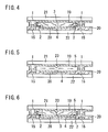
- FIG. 39 In the cross sectional view of FIG. 39 , there are shown an upper glass substrate 221 , a lower glass substrate 222 , a signal electrode line 215 , a lower transparent electrode, that is, a pixel electrode, 220 , an upper transparent electrode, that is, an opposing electrode 219 , a black mask 231 , a color layer 232 , an overcoat 233 , a lower silicon nitride film 204 , and an upper silicon nitride film 241 .
- the black mask 231 for shutting out the light
- the color layer 232 for passing the light of predetermined color
- the overcoat 233 for protecting the black mask 231 and the color layer 232
- the opposing electrode 219 there are disposed, on the upper glass substrate 221 , the black mask 231 for shutting out the light, the color layer 232 for passing the light of predetermined color, the overcoat 233 for protecting the black mask 231 and the color layer 232 , and the opposing electrode 219 .
- the signal electrode line 215 On the lower glass substrate 222 , there are disposed, on the side facing toward the upper glass substrate 221 , the signal electrode line 215 , the lower silicon nitride film 204 for covering the lower glass substrate 222 and the signal electrode line 215 , the pixel electrode 220 formed on the lower silicon nitride film 204 , and the upper silicon nitride film 241 covering whole portion on the lower glass substrate 222 .
- electric field 202 is shown by arrows which is produced when a voltage is applied to the liquid crystal display element having the structure shown in FIG. 39 .
- FIG. 41 In the cross sectional view of FIG. 41 , there are shown an upper glass substrate 221 , a lower glass substrate 222 , a signal electrode line 215 , a lower transparent electrode, that is, a pixel electrode, 220 , an upper transparent electrode, that is, an opposing electrode 229 , a black mask 231 , a color layer 232 , an overcoat 233 , a lower silicon nitride film 204 , and an upper silicon nitride film 241 .
- the black mask 231 for shutting out the light
- the color layer 232 for passing the light of predetermined color
- the overcoat 233 for protecting the black mask 231 and the color layer 232
- the opposing electrode 229 On the upper glass substrate 221 , there are disposed, on the side facing toward the lower glass substrate 222 , the black mask 231 for shutting out the light, the color layer 232 for passing the light of predetermined color, the overcoat 233 for protecting the black mask 231 and the color layer 232 , and the opposing electrode 229 .
- the signal electrode line 215 On the lower glass substrate 222 , there are disposed, on the side facing toward the upper glass substrate 221 , the signal electrode line 215 , the lower silicon nitride film 204 for covering the lower glass substrate 222 and the signal electrode line 215 , the pixel electrode 220 formed on the lower silicon nitride film 204 , and the upper silicon nitride film 241 covering whole portion on the lower glass substrate 222 .
- electric field 202 is shown by arrows which is produced when a voltage is applied to the liquid crystal display element having the structure shown in FIG. 41 .
- the first problem in the above-mentioned prior art liquid crystal display element is that disturbance of alignment which is called disclination and which is caused by lateral electric field between the wiring electrode and the pixel electrode.
- disclination disturbance of alignment
- lateral electric field between the wiring electrode and the pixel electrode.
- potential of the wiring electrode such as the scanning electrode line, the signal electrode line and the like gives large influence on the electric field.
- relatively large lateral electric field is produced and liquid crystal alignment is changed by such lateral electric field.
- the second problem in the above-mentioned prior art liquid crystal display element is that, when pressure is applied from the outside to the liquid crystal display panel having such liquid crystal display element by pressing the panel by a finger or by a pen point, alignment of liquid crystal molecules is easily disturbed, or alignment division collapses or becomes defective.
- This liquid crystal display comprises a plurality of liquid crystal regions each of which has an electrode, is disposed between a pair of substrates, at least one of the substrates being transparent, and is surrounded by the high polymer material.
- This liquid crystal display also comprises a light control layer which is disposed between the surface of at least one substrate and an electrode formed on the substrate, which controls an intensity of incident light by changing transmittance and which has locally different film thickness. Also, the space between the electrodes on respective surfaces of the pair of substrates varies corresponding to the change of the film thickness of the light control layer.
- the liquid crystal display device disclosed in this application has a pair of opposing substrates each of which comprises a transparent electrode formed on the surface thereof and an alignment film formed on the transparent electrode, and a liquid crystal layer of liquid crystal molecules filling the space between the substrates.
- TN twisted nematic
- a direction of an alignment vector of the liquid crystal molecules is parallel to a surface of a substrate and this condition corresponds to the condition in which “white” is displayed.
- the direction of the alignment vector varies toward a direction of an electric field according to a voltage applied. Thereby, the condition in which “white” is displayed is gradually changed to the condition in which “black” is displayed.
- a liquid crystal display panel of the structure shown in these drawings comprises an upper substrate having a color filter substrate 501 and having a common electrode 502 and an alignment layer 503 which are formed on the color filter substrate and which have a slit 517 formed in the common electrode 502 and the alignment layer 503 . Also, there is provided a lower substrate having a substrate 507 , a pixel electrode 504 formed on the substrate 507 and an alignment layer 503 formed on the pixel electrode 504 . A space between the upper substrate and the lower substrate is filled with liquid crystal molecules 508 which are homeotropic aligned and which form a liquid crystal layer.
- the liquid crystal display panel shown in FIG. 44A , FIG. 44B and FIG. 44C is put between a pair of polarizers disposed such that polarizing axes or transmission axes of these polarizers have right angles with each other.
- a voltage is applied between the common electrode 502 and the pixel electrode 504 , an electric field having slant components is produced. Therefore, more than one liquid crystal domains having different alignment directions are produced in each pixel, and thereby viewing angle characteristics are improved.
- the shape of the slit can be, for example, a rectangle as shown in FIG. 44B , or can be x-shape as shown in FIG. 44C .
- each pixel is divided into more than one domains by using an electric field having slant and different components to improve viewing angle characteristics.
- Japanese patent laid-open publication No. 10-20323 there is disclosed a liquid crystal display in which more than one kind of minute domains coexist in a liquid crystal layer.
- One of substrates of liquid crystal display panel of this liquid crystal display has opening portions, and there is provided a second electrode in each of the opening portions.
- a voltage is applied to the second electrode to produce an electric field having slant components.
- domains having different alignment directions are produced in each pixel and wide viewing angle characteristics are obtained.
- This publication mainly concerns a liquid crystal display having TN type cell.
- Japanese PCT patent laid-open publication No. 5-505247 discloses a liquid crystal display of In-Plain-Switching (IPS) system or mode in which, in order to rotate liquid crystal molecules while keeping the liquid crystal molecules in a direction parallel to substrates of liquid crystal display panel, two electrodes are disposed on one of the substrates. A voltage is applied to between the two electrodes and, thereby, an electric field parallel to the substrates is produced.
- IPS In-Plain-Switching
- a long axis of each of liquid crystal molecules does not rise from the substrate when the voltage is applied. Therefore, when a viewing angle is changed, variation of birefringence or double refraction of liquid crystal is relatively small and, therefore, wide viewing angle characteristics are obtained.
- liquid crystal display which has the above-mentioned IPS mode and in which liquid crystal molecules having a positive anisotropy of permittivity are aligned as homeotropic alignment.
- the liquid crystal molecules are rotated toward a direction parallel to the substrate by using an electric field parallel to the substrate.
- the liquid crystal molecules which are homeotropic aligned are grouped into two domains.
- the two domains have different alignment directions of liquid crystal molecules and, therefore, it is possible to obtain a liquid crystal display having wide viewing angle characteristics.
- Japanese patent laid-open publication No. 10-186330 proposes a liquid crystal display in which square wall structures are produced by using a photosensitive material, and a pixel is formed by using each of such structures as a basic unit. When a voltage is applied to produce an electric field, liquid crystal molecules having a negative anisotropy of permittivity are rotated toward different directions in a pixel.
- active elements such as thin film diodes and the like are formed on one of transparent substrates. Therefore, it is only necessary to perform a microfabrication process, such as photolithography and the like, on one of the substrate on which active elements are formed. It is not necessary to perform such microfabrication process on the other substrate which is usually called a “common electrode”, but it is only necessary to form an electrode on whole area of the other substrate.
- a liquid crystal display comprising: an upper substrate and a lower substrate, wherein at least one of the upper substrate and lower substrate is a transparent substrate; an upper electrode disposed on the surface of the upper substrate which surface of the upper substrate opposes to the lower substrate, and a lower electrode disposed on the surface of the lower substrate which surface of the lower substrate opposes to the upper substrate, wherein at least one of the upper electrode and lower electrode disposed on the transparent substrate is transparent; a liquid crystal material disposed between the upper electrode and the lower electrode; a scanning electrode line and a signal electrode line disposed on the surface of the lower substrate which surface of the lower substrate opposes to the upper substrate; a switching element for controlling application of a voltages to the lower electrode, wherein the application of a voltage to the lower electrode by the switching element is controlled by application of voltages to the scanning electrode line and the signal electrode line; and a conductive protrusion disposed on the surface of the upper substrate which surface of the upper substrate opposes to the lower substrate, where
- the conductive protrusion comprises: a protruded portion disposed on the surface of the upper substrate which surface of the upper substrate opposes to the lower substrate, the protruded portion being disposed over the scanning electrode line or the signal electrode line; and a part of the upper electrode covering the protruded portion.
- the upper substrate is an upper transparent substrate and the conductive protrusion comprises: a protruded portion disposed on the surface of the upper transparent substrate which surface of the upper substrate opposes to the lower substrate, the protruded portion being disposed over the scanning electrode line or the signal electrode line; and a part of the upper transparent electrode covering a side surface of the protruded portion.
- the protruded portion comprises color filter layers or transparent resin layers which are piled on the surface, of the upper transparent substrate opposing to the lower substrate.
- the width of the conductive protrusion is substantially equal to or larger than the width of the scanning electrode line or the signal electrode line.
- the liquid crystal display further comprises a lower insulating film which covers the scanning electrode line and the signal electrode line and which contacts with the conductive protrusion.
- At least one of the upper electrode and the lower electrode further comprises a projection which is different from the conductive protrusion and which is used for dividing alignment of the liquid crystal material.
- At least one of the upper electrode and the lower electrode further comprises a nonconductive opening portion which is used for dividing alignment of the liquid crystal material.
- the conductive protrusion is electrically coupled with the scanning electrode line or the signal electrode line.
- the liquid crystal display further comprises a conductive contact portion disposed on the scanning electrode line or the signal electrode line, wherein the conductive protrusion and the conductive contact portion contact with each other.
- the liquid crystal display further comprises spacers dispersed in a space between the upper substrate and the lower substrate.
- the liquid crystal display has a plurality of pixel areas surrounded by the scanning electrode lines and signal electrode lines; the lower electrode comprises a plurality of pixel electrodes each corresponding to the pixel area; each of the pixel area has a predetermined symmetry center point; and the conductive protrusions are disposed centrosymmetrically with respect to the symmetry center point.
- the symmetry center point is substantially in the center of a corresponding pixel area.
- At least one of the upper electrode and the pixel electrode further comprises a projection which is different from the conductive protrusion and which is used for dividing alignment of the liquid crystal material, and wherein the projection is disposed on a predetermined line which substantially passes the symmetry center point.
- At least one of the upper electrode and the lower electrode further comprises a nonconductive opening portion which is used for dividing alignment of the liquid crystal material, and wherein the nonconductive opening portion is disposed on a predetermined line which substantially passes the symmetry center point.
- the liquid crystal display has a plurality of pixel areas surrounded by the scanning electrode lines and signal electrode lines; the lower electrode comprises a plurality of pixel electrodes each corresponding to the pixel area; each of the pixel area has a predetermined symmetry center line; and the conductive protrusions are disposed symmetrically with respect to the symmetry center line.
- the symmetry center line is substantially passes the center of a corresponding pixel area.
- At least one of the upper electrode and the pixel electrode further comprises a projection which is different from the conductive protrusion and which is used for dividing alignment of the liquid crystal material, and wherein the projection is disposed substantially on the symmetry center line.
- At least one of the upper electrode and the lower electrode further comprises a nonconductive opening portion which is used for dividing alignment of the liquid crystal material, and wherein the nonconductive opening portion is disposed substantially on the symmetry center line.
- the liquid crystal material is a nematic liquid crystal material, a cholesteric liquid crystal material, or a discotic liquid crystal material.
- an operation mode of the liquid crystal material is twisted nematic, STN super twisted nematic, homogeneous, homeotropic, in-plain switching, ⁇ -cell, cholesteric phase transition, polymer dispersion, or polymer network.
- a method of manufacturing a liquid crystal display comprising: (a) forming a wiring electrode line on the surface of a lower substrate which surface of the lower substrate opposes to an upper substrate, forming an insulating film covering the wiring electrode line, forming a lower electrode on the insulating film, and forming a switching element for applying a voltage to the lower electrode; (b) forming a protruded portion on the surface of the upper substrate which surface of the upper substrate opposes to the lower substrate, wherein the protruded portion is located substantially just above the wiring electrode line when the lower substrate and the upper substrate are opposed to each other; (c) forming an upper electrode covering whole portion of the protruded portion and the surface of the upper substrate which surface of the upper substrate opposes to the lower substrate, wherein at least one of the upper substrate and the lower substrate is a transparent substrate, and at least one of the upper electrode and lower electrode disposed on the transparent substrate is transparent; (d) opposing the lower substrate and the upper substrate such
- the step (b) comprises forming the protruded portion by piling a plurality of color filters on the surface of the upper substrate which surface of the upper substrate opposes to the lower substrate.
- the step (b) comprises piling a plurality of transparent resin layers on the surface of the upper substrate which surface of the upper substrate opposes to the lower substrate and removing piled transparent resin layers except portions corresponding to the protruded portions.
- the width of the protruded portion is substantially equal to or larger than the width of the wiring electrode line.
- the method further comprises: (f) forming a projection which is different from the protruded portion on at least one of the upper electrode and the lower electrode.
- the method further comprises: (g) removing a portion of at least one of the upper electrode and the lower electrode.
- the method further comprises: (h) forming a conductive contact portion on the wiring electrode line, the conductive contact portion being electrically coupled with the wiring electrode line; wherein the step (d) further comprises disposing the conductive contact portion and the upper electrode covering the protruded portion such that the conductive contact portion and the upper electrode covering the protruded portion contact with each other.
- a method of manufacturing a liquid crystal display having a plurality of pixel areas comprising: (a) forming wiring electrode lines on the surface of a lower substrate which surface of the lower substrate opposes to an upper substrate such that the wiring electrode lines surround respective pixel areas, forming an insulating film covering the wiring electrode lines, forming, for each pixel area, a pixel electrode which does not coupled with the wiring electrode line, and forming a switching element for controlling an application of a voltage to the pixel electrode; (b) forming protruded portions on the surface of the upper substrate which surface of the upper substrate opposes to the lower substrate, wherein the protruded portions are located at portions centrosymmetrical with respect to a predetermined symmetry center point in each pixel area, and are located substantially just above the wiring electrode lines when the lower substrate and the upper substrate are opposed to each other; (c) forming an upper electrode covering whole portion of the protruded portions and the surface of the upper substrate which surface of the upper substrate which surface of the upper
- the symmetry center point is substantially in the center of a corresponding pixel area.
- the method further comprises: (f) forming a projection which is different from the protruded portion on the surface of the upper substrate which surface of the upper substrate opposes to the lower substrate; wherein the step (c) comprises forming an upper transparent electrode covering the surface of the upper substrate which surface of the upper substrate opposes to the lower substrate, the protruded portion and the projection.
- the step (f) comprises forming a projection which is different from the protruded portion on the surface of the upper substrate which surface of the upper substrate opposes to the lower substrate such that the projection is located on a predetermined line substantially passing through the symmetry center point.
- the method further comprises: (g) removing a portion of the upper electrode except the protruded portion.
- step (g) comprises removing the upper electrode existing on a predetermined line substantially passing through the symmetry center point.
- the method further comprises: (h) removing a portion of the lower electrode.
- the step (h) comprises removing the lower electrode existing on a predetermined line substantially passing through the symmetry center point.
- a method of manufacturing a liquid crystal display having a plurality of pixel areas comprising: (a) forming wiring electrode lines on the surface of a lower substrate which surface of the lower substrate opposes to an upper substrate such that the wiring electrode lines surround respective pixel areas, forming an insulating film covering the wiring electrode lines, forming, for each pixel area, a pixel electrode which does not coupled with the wiring electrode line, and forming a switching element for controlling an application of a voltage to the pixel electrode; (b) forming protruded portions on the surface of the upper substrate which surface of the upper substrate opposes to the lower substrate, wherein the protruded portions are located at portions symmetrical with respect to a predetermined symmetry center line in each pixel area and are located substantially just above the wiring electrode lines when the lower substrate and the upper substrate are opposed to each other; (c) forming an upper electrode covering whole portion of the protruded portions and the surface of the upper substrate which surface of the upper substrate oppose
- the symmetry center line is substantially in the center of a corresponding pixel area.
- the method further comprises: (f) forming a projection which is different from the protruded portion on the surface of the upper substrate which surface of the upper substrate opposes to the lower substrate; wherein the step (c) comprises forming an upper transparent electrode covering the surface of the upper substrate which surface of the upper substrate opposes to the lower substrate, the protruded portion and the projection.
- the step (f) comprises forming a projection which is different from the protruded portion on the surface of the upper substrate which surface of the upper substrate opposes to the lower substrate such that the projection is substantially located on the symmetry center line.
- the method further comprises: (g) removing a portion of the upper electrode except the protruded portion.
- step (g) comprises removing the upper electrode substantially existing on the symmetry center line.
- the method further comprises: (h) removing a portion of the lower electrode.
- step (h) comprises removing the lower electrode substantially existing on the symmetry center line.
- the method further comprises forming spacers dispersed in a space between the upper substrate and the lower substrate.
- the liquid crystal material is a nematic liquid crystal material, a cholesteric liquid crystal material, or a discotic liquid crystal material.
- an operation mode of the liquid crystal material is twisted nematic, STN super twisted nematic, homogeneous, homeotropic, in-plain switching, ⁇ -cell, cholesteric phase transition, polymer dispersion, or polymer network.
- a liquid crystal display comprising: a first substrate having a common electrode formed thereon; a second substrate opposed to the first substrate and having a plurality of pixel electrodes formed thereon; and a liquid crystal layer disposed between the first and second substrates; wherein each of the pixel electrodes has a smaller area than that of the common electrode and is covered by the common electrode, and each of the pixel electrode comprises an electrode portion having approximately symmetrical shape.
- the shape of the electrode portion of the pixel electrode is a circle, an ellipse or a polygon.
- each of the pixel electrode is formed as a link of a plurality of electrode areas each having approximately symmetrical shape, and each of the pixel electrodes has a smaller area than that of the common electrode and is covered by the common electrode.
- the common electrode is formed on approximately whole area of the first substrate.
- the liquid crystal display further comprises a shield electrode formed around the pixel electrode.
- a common electrode for applying a reference potential over a plurality of pixels
- a plurality of scanning signal electrodes for applying a reference potential over a plurality of pixels
- a plurality of image signal electrodes which cross the scanning signal electrodes to form a matrix
- a plurality of thin film transistors each formed corresponding an intersection of the scanning signal electrode and the image signal electrode
- at least one pixel is formed in each of areas surrounded by the a plurality of scanning signal electrodes and the a plurality of image signal electrode, and each pixel comprises a pixel electrode coupled with the thin film transistor corresponding to the pixel
- the pixel electrode is isolated via an interlayer insulating film from the scanning signal electrode, the image signal electrode and the thin film transistor.
- a common electrode for applying a reference potential over a plurality of pixels
- a plurality of scanning signal electrodes for applying a reference potential over a plurality of pixels
- a plurality of image signal electrodes which cross the scanning signal electrodes to form a matrix
- a plurality of thin film transistors each formed corresponding to an intersection of the scanning signal electrode and the image signal electrode
- at least one pixel is formed in each of areas surrounded by the plurality of scanning signal electrodes and the plurality of image signal electrode, and each pixel comprises a pixel electrode coupled with the thin film transistor corresponding to the pixel
- the pixel electrode is isolated via an interlayer insulating film from the scanning signal electrode, the image signal electrode and the thin film transistor
- the liquid crystal display further comprises a color filter layer disposed on the second substrate, wherein the liquid crystal layer being disposed between the color filter layer and the first substrate; wherein, on the second substrate, there are formed a plurality of scanning signal electrodes, a plurality of image signal electrodes which cross the scanning signal electrodes to form a matrix, and a plurality of thin film transistors each formed corresponding to an intersection of the scanning signal electrode and the image signal electrode; wherein at least one pixel is formed in each of areas surrounded by the plurality of scanning signal electrodes and the plurality of image signal electrodes, and each pixel comprises a pixel electrode coupled with the thin film transistor corresponding to the pixel; wherein the common electrode on the first substrate provides a reference potential for a plurality of pixels; and wherein the pixel electrode is disposed between the color filter layer and the liquid crystal layer.
- the liquid crystal display further comprises a color filter layer disposed on the second substrate, wherein the liquid crystal layer being disposed between the color filter layer and the first substrate; wherein, on the second substrate, there are formed a plurality of scanning signal electrodes, a plurality of image signal electrodes which cross the scanning signal electrodes to form a matrix, and a plurality of thin film transistors each formed corresponding to an intersection of the scanning signal electrode and the image signal electrode; wherein at least one pixel is formed in each of areas surrounded by the plurality of scanning signal electrodes and the plurality of image signal electrodes, and each pixel comprises a pixel electrode coupled with the thin film transistor corresponding to the pixel; wherein the common electrode on the first substrate provides a reference potential for a plurality of pixels; wherein the pixel electrode is disposed between the color filter layer and the liquid crystal layer; and wherein, on at least one of the scanning signal electrode and the image signal electrode, there is disposed a portion of the pixel electrode or a shielding electrode.
- the electrode portion of the pixel electrode has an approximately symmetrical shape with notches or protrusions extending radially from the center of the approximately symmetrical shape.
- the electrode portion of the pixel electrode has an approximately symmetrical shape with voids in which no electrode material exists and which extend radially from the center of the approximately symmetrical shape.
- the electrode portion of the pixel electrode has an approximately symmetrical shape with concave portions which extend radially from the center of the approximately symmetrical shape.
- the concave portions are formed in an interlayer insulating layer or in an overcoating layer.
- At least one of an optically negative compensation film and an optically positive compensation film between the first or second substrate and a polarizer, thereby making anisotropy of refractive index of the liquid crystal layer and the compensation film isotropic.
- the liquid crystal layer includes organic polymer compound.
- the liquid crystal layer comprises a liquid crystal material having a negative anisotropy of permittivity, and liquid crystal molecules of the liquid crystal material align approximately perpendicular to the first and second substrates when no voltage is applied thereto.
- a pretilt angle of liquid crystal molecules in the liquid crystal layer is previously provided along a direction toward which the liquid crystal molecules rotate when a voltage is applied thereto.
- the liquid crystal display further comprises quarter-wave plates on both sides of the liquid crystal layer, and optical axes of the quarter-wave plates are perpendicular to each other.
- the liquid crystal display further comprises quarter-wave plates on both sides of the liquid crystal layer, and optical axes of the quarter-wave plates are perpendicular to each other.
- the liquid crystal layer comprises a liquid crystal material having a positive anisotropy of permittivity, and liquid crystal molecules of the liquid crystal material have a twisted nematic structure when no voltage is applied thereto.
- the liquid crystal layer comprises a liquid crystal material having a positive anisotropy of permittivity, and liquid crystal molecules of the liquid crystal material have a homogeneous structure when no voltage is applied thereto.
- a pretilt angle of the liquid crystal layer with respect to the first and second substrates is equal to or smaller that 1 (one) degree.
- a method of manufacturing a liquid crystal display comprising: preparing a first substrate having a common electrode formed thereon and a second substrate opposed to the first substrate and having a plurality of pixel electrodes formed thereon, wherein each of the pixel electrodes has a smaller area than that of the common electrode and is covered by the common electrode, and each of the pixel electrode comprises an electrode portion having approximately symmetrical shape; injecting a liquid crystal material containing liquid crystal molecules and monomer and/or oligomer into a space between the first and second substrates; and polymerizing the monomer and/or oligomer.
- the monomer and/or oligomer is polymerized while irradiating light thereon, thereby a pretilt angle is formed in the liquid crystal molecules.
- the light is irradiated at a slant angle with respect to the substrate.
- the light is polarized light.
- the polarized light is irradiated from a direction approximately perpendicular to the substrate, thereby making a pretilt angle of liquid crystal molecules equal to or smaller than 1 degree.
- a method of driving the above-mentioned liquid crystal display in which a light shield layer is provided at a portion of each pixel in which leakage of light occurs when a voltage near the threshold voltage of liquid crystal molecules is applied.
- FIG. 1 is a schematic cross sectional view showing a portion including approximately one pixel of a liquid crystal display according to the first embodiment of the present invention
- FIG. 2 is a schematic cross sectional view illustrating an operation of the liquid crystal display according to the first embodiment
- FIG. 3 is a schematic cross sectional view showing a portion including approximately one pixel of a liquid crystal display according to the second embodiment of the present invention
- FIG. 4 is a schematic cross sectional view illustrating an operation of the liquid crystal display according to the second embodiment
- FIG. 5 is a schematic cross sectional view showing a portion including approximately one pixel of a liquid crystal display according to the fourth embodiment of the present invention.
- FIG. 6 is a schematic cross sectional view illustrating an operation of the liquid crystal display according to the fourth embodiment.
- FIG. 7 is a top perspective plan view showing a portion including approximately one pixel of a liquid crystal display according to the fifth embodiment of the present invention.
- FIG. 8 is a top perspective plan view showing a portion including approximately one pixel of a liquid crystal display according to the sixth embodiment of the present invention.
- FIG. 9 is a top perspective plan view showing a portion including approximately one pixel of a liquid crystal display according to a variation of the sixth embodiment of the present invention.
- FIG. 10 is a schematic cross sectional view showing a portion including approximately one pixel of a liquid crystal display according to the seventh embodiment of the present invention.
- FIG. 11 is a schematic cross sectional view illustrating an operation of the liquid crystal display according to the seventh embodiment.
- FIG. 12 is a schematic cross sectional view showing a portion including approximately one pixel of a liquid crystal display according to the eighth embodiment of the present invention.
- FIG. 13 is a schematic cross sectional view showing a portion including approximately one pixel of a liquid crystal display according to the ninth embodiment of the present invention.
- FIG. 14 is a top perspective plan view showing a portion including approximately one pixel of a liquid crystal display according to the seventh practical example of the present invention.
- FIG. 15A is a schematic cross sectional view showing a portion including approximately one pixel of a liquid crystal display according to the twelfth embodiment of the present invention.
- FIG. 15B is a schematic plan view showing a liquid crystal display according to the twelfth embodiment of the present invention.
- FIG. 15C shows examples of schematic shapes of pixel electrodes used in the liquid crystal display according to the present invention.
- FIG. 16 shows examples of schematic shapes of pixel electrodes in which symmetrical shapes are combined and which are used in the liquid crystal display according to the present invention
- FIG. 17 shows examples of schematic shapes of pixel electrodes in which notches are provided and which are used in the liquid crystal display according to the present invention
- FIG. 18 shows examples of schematic shapes of pixel electrodes in which protrusions are provided and which are used in the liquid crystal display according to the present invention
- FIG. 19 shows examples of schematic shapes of pixel electrodes in which voids are provided and which are used in the liquid crystal display according to the present invention
- FIG. 20 shows examples of schematic shapes of pixel electrodes in which concave portions are provided and which are used in the liquid crystal display according to the present invention
- FIG. 21A is a schematic cross sectional view showing a portion including approximately one pixel of a liquid crystal display according to the thirteenth embodiment of the present invention.
- FIG. 21B is a schematic plan view showing a pixel area which includes divided domains having different alignment directions in a liquid crystal display according to the thirteenth embodiment of the present invention.
- FIG. 22A is a schematic cross sectional view showing a portion including approximately one pixel of a liquid crystal display according to a variation of the thirteenth embodiment of the present invention.
- FIG. 22B is a schematic plan view showing a pixel area which includes divided domains having different alignment directions in a liquid crystal display according to the variation of the thirteenth embodiment of the present invention.
- FIG. 23A is a schematic cross sectional view showing a portion including approximately one pixel of a liquid crystal display according to the fourteenth embodiment of the present invention.
- FIG. 23B is a schematic plan view showing a pixel area which includes divided domains having different alignment directions in a liquid crystal display according to the fourteenth embodiment of the present invention.
- FIG. 24A is a schematic cross sectional view showing a portion including approximately one pixel of a liquid crystal display according to a variation of the fourteenth embodiment of the present invention.
- FIG. 24B is a schematic plan view showing a pixel area which includes divided domains having different alignment directions in a liquid crystal display according to the variation of the fourteenth embodiment of the present invention.
- FIG. 25A is a schematic cross sectional view showing a portion including approximately one pixel of a liquid crystal display according to another variation of the fourteenth embodiment of the present invention.
- FIG. 25B is a schematic plan view showing a pixel area which includes divided domains having different alignment directions in a liquid crystal display according to another variation of the fourteenth embodiment of the present invention.
- FIG. 26A is a schematic cross sectional view showing a portion including approximately one pixel of a liquid crystal display according to the fifteenth embodiment of the present invention.
- FIG. 26B is a schematic plan view showing a pixel area which includes divided domains having different alignment directions in a liquid crystal display according to the fifteenth embodiment of the present invention.
- FIG. 27A is a schematic cross sectional view showing a portion including approximately one pixel of a liquid crystal display according to the sixteenth embodiment of the present invention.
- FIG. 27B is a schematic plan view showing a pixel area which includes divided domains having different alignment directions in a liquid crystal display according to the sixteenth embodiment of the present invention.
- FIG. 28 is a plan view of a conventional liquid crystal display disclosed in Japanese patent laid-open publication No. 63-106624;
- FIG. 29 is a perspective view of a conventional liquid crystal display disclosed in Japanese patent laid-open publication No. 63-106624;
- FIG. 30 is a cross sectional view taken on line a-a′ of FIG. 28 ;
- FIG. 31 is a perspective plan view showing rubbing directions and twist of liquid crystal molecules between an upper substrate and a lower substrate when the liquid crystal display of FIG. 29 is observed from a bearing angle which is changed by 45 degrees;
- FIG. 32 is a cross sectional view taken on line b-b′ of FIG. 31 ;
- FIG. 33 is a perspective plan view showing rubbing directions and twist of liquid crystal molecules between an upper substrate and a lower substrate in a liquid crystal display shown in SID '92 Digest, p. 798;
- FIG. 34 is a cross sectional view taken on line c-c′ of FIG. 33 ;
- FIG. 35 is a perspective plan view showing rubbing directions and twist of liquid crystal molecules between an upper substrate and a lower substrate in a liquid crystal display shown in Japan Display '92 Digest, p. 591;
- FIG. 36 is a cross sectional view taken on line d-d′ of FIG. 33 ;
- FIG. 37 is a perspective plan view showing rubbing directions and twist of liquid crystal molecules between an upper substrate and a lower substrate in a liquid crystal display shown in SID '92 Digest, p. 269;
- FIG. 38 is a cross sectional view taken on line d-d′ of FIG. 37 ;
- FIG. 39 is a partial cross sectional view showing a conventional liquid crystal display shown in Conference Record of the 1991 International Display Research Conference, p. 239;
- FIG. 40 is a schematic cross sectional view showing a condition of lateral electric field in the liquid crystal display shown in FIG. 39 ;
- FIG. 41 is a schematic cross sectional view showing a portion including approximately one pixel of a conventional TN type liquid crystal display
- FIG. 42 is a schematic cross sectional view showing a condition of electric field in the liquid crystal display shown in FIG. 41 ;
- FIG. 43 is a schematic cross sectional view illustrating an operation of a conventional liquid crystal display
- FIG. 44A is a schematic cross sectional view showing a portion including approximately one pixel of a conventional liquid crystal display
- FIG. 44B is a schematic plan view showing an example of a pixel area in the conventional liquid crystal display FIG. 44A ;
- FIG. 44C is a schematic plan view showing another example of a pixel area in the conventional liquid crystal display FIG. 44A ;
- FIG. 45 includes photographs showing variation of liquid crystal alignment in a pixel of a liquid crystal display according to the Example 18.
- FIG. 1 illustrates a schematic cross section of a portion including approximately one pixel of a liquid crystal display element according to the first embodiment.
- the liquid crystal display element according to the first embodiment comprises a pair of opposing transparent substrates 21 and 22 , and liquid crystal material 5 filling the space between the pair of transparent substrates 21 and 22 .
- the pair of opposing transparent substrates 21 and 22 constitute an upper substrate 21 and a lower substrate 22 .
- the liquid crystal material 5 can be any of nematic liquid crystal material, cholesteric or chiralsmectic liquid crystal material, discotic liquid crystal material.
- Operation mode of the liquid crystal material 5 may be any of TN (Twisted Nematic), STN (Super Twisted Nematic), homogeneous, homeotropic, IPS (In-Plain Switching), ⁇ -cell or OCB (Optically Compensated Bend), cholesteric phase transition, PDLC (polymer dispersed liquid crystal), polymer network, and the like.
- TN Transmission Nematic
- STN Super Twisted Nematic
- IPS In-Plain Switching
- ⁇ -cell or OCB Optically Compensated Bend
- cholesteric phase transition cholesteric phase transition
- PDLC polymer dispersed liquid crystal
- polymer network and the like.
- a pretilt angle 51 of the liquid crystal material 5 that is, an angle between liquid crystal molecules and the substrate surface, may be any value.
- each pixel includes a switching element not shown in the drawing, and application of a signal voltage to each pixel electrode 20 is performed via the switching element and is controlled by the switching element.
- switching element there is a TFT (Thin Film Transistor) whose gate electrode is constituted of the scanning electrode line, whose source electrode is coupled with the signal line, and whose drain electrode is coupled with the pixel electrode 20 .
- an opposing electrode 19 and uneven structures 1 such as protrusions or bumps (only one of such uneven structures is shown in FIG. 1 ).
- the uneven structure 1 is disposed over the wiring electrode 15 .
- the opposing electrode 19 is made of transparent material. Also, the opposing electrode 19 is formed such that the opposing electrode 19 wholly covers the upper substrate 21 and the uneven structure 1 .
- the uneven structure 1 can be disposed on every wiring electrode 15 .
- the uneven structure 1 can be disposed on each one of some wiring electrodes 15 .
- a liquid crystal display element having three wiring electrodes corresponding to three pixels of red, blue and green it is possible to dispose one uneven structure 1 on any one of the three wiring electrodes.
- a portion of the transparent electrode 19 located under the uneven structure 1 contacts the lower substrate 22 .
- the width of the portion where the transparent electrode 19 and the lower substrate 22 contact each other is wider than the width of the wiring electrode 15 . It is also possible for the width of the portion where the transparent electrode 19 and the lower substrate 22 contact each other to be substantially equal to the width of the wiring electrode 15 .
- lateral electric field produced in the liquid crystal display device can be more effectively controlled in the structure in which the width of the portion where the transparent electrode 19 and the lower substrate 22 contact each other is wider than the width of the wiring electrode 15 than in the structure in which the width of the portion where the transparent electrode 19 and the lower substrate 22 contact each other is substantially equal to the width of the wiring electrode 15 .
- the wiring electrodes 15 are formed on the lower transparent substrate 22 by using a known method. For example, a chromium (Cr) layer is formed on the lower transparent substrate 22 , and the chromium layer thus formed is patterned to form the wiring electrodes 15 .
- a chromium (Cr) layer is formed on the lower transparent substrate 22 , and the chromium layer thus formed is patterned to form the wiring electrodes 15 .
- the insulating layer 4 is then formed such that the insulating layer 4 wholly covers the lower transparent substrate 22 including the wiring electrodes 15 formed on the lower substrate 22 .
- the pixel electrode that is, the lower transparent electrode 20 is formed by using a well known method.
- the switching element such as the TFT and the like for applying a signal voltage from the wiring electrode 15 to the lower transparent electrode 20 is formed by using a well known method.
- the uneven structure, that is, a protrusion, 1 is formed on the upper transparent substrate 21 .
- such protrusion 1 can be formed by using any of methods described below. That is, when a color filter not shown in the drawing is formed on the upper transparent substrate, such color filter is repeatedly formed and stacked in the region where the protrusion 1 is to be formed, thereby the protrusion 1 having a predetermined height is formed. It is also possible to stack transparent resin material in the region where the protrusion 1 is to be formed to obtain the protrusion 1 having a predetermined height. Further, it is possible to form a transparent resin layer having a predetermined thickness on the upper transparent substrate and to pattern the transparent resin layer to leave the protrusion 1 only in the region where the protrusion 1 is to be formed.
- the upper transparent electrode 19 is formed which wholly covers the upper transparent substrate 21 and the protrusion 1 , by using a well known method.
- the lower transparent substrate 22 and the upper transparent substrate 21 are disposed such that the lower transparent electrode 20 and the upper transparent electrode 19 are opposed to each other, and both substrates 22 and 21 are coupled and sealed at the peripheral portion thereof.
- liquid crystal material 5 is injected between the lower transparent substrate 22 and the upper transparent substrate 21 by using a vacuum injection method.
- the liquid crystal display element according to the first embodiment of the present invention is fabricated.
- FIG. 2 is a cross sectional view used for illustrating an operation of the liquid crystal display element according to the first embodiment.
- an illustration of lateral electric field designated by an arrow 2 and an illustration of a disclination line designated by a dotted line 3 are added to the cross sectional view of FIG. 1 .
- the disclination line 3 is a kind of defect of crystal alignment arising at a boundary between or among a plurality of adjacent domains having different alignment of liquid crystal molecules.
- the disclination line 3 does not exist on the pixel electrode 20 .
- FIG. 43 shows a schematic cross sectional structure of a conventional liquid crystal display element.
- the conventional liquid crystal display element shown in FIG. 43 comprises a pair of opposing transparent substrates 321 and 322 , and liquid crystal material 305 filling the space between the pair of transparent substrates 321 and 322 .
- the pair of opposing transparent substrates 321 and 322 constitute an upper substrate 321 and a lower substrate 322 .
- the wiring electrodes 315 are scanning electrode lines or signal electrode lines.
- the pixel electrodes 320 are composed of transparent material.
- the wiring electrodes 315 and the pixel electrodes 320 are mutually insulated or isolated by the insulating layer 304 .
- an opposing electrode 319 On a surface of the upper substrate 321 which faces toward the lower substrate 322 , there is formed an opposing electrode 319 .
- the opposing electrode 319 is made of transparent material. Also, the opposing electrode 319 is formed such that the opposing electrode 319 wholly covers the upper substrate 321 .
- FIG. 43 there are also shown lateral electric field 302 and a disclination line 303 during operation of the liquid crystal display element. From FIG. 43 , it can be seen that the disclination line 303 exists on the pixel electrode 320 in the conventional liquid crystal display element.
- the liquid crystal display element according to the first embodiment of the present invention comprises, as mentioned above, the uneven structure 1 in addition to the structure of the conventional liquid crystal display element shown in FIG. 43 .
- the intensity of the lateral electric field 2 arising in the liquid crystal display element according to this embodiment of the present invention is very weak when compared with the lateral electric field 302 arising in the conventional liquid crystal display element shown in FIG. 43 . That is, the potential difference between the pixel electrode 20 and the wiring electrode 15 is usually much larger than the potential difference between the pixel electrode 20 and the opposing electrode 19 .
- the uneven structure 1 is covered by the opposing electrode 19 and is disposed on the wiring electrode 15 and, therefore, the lateral electric field 2 in the liquid crystal display element according to this embodiment is mainly caused by the potential difference between the pixel electrode 20 and the opposing electrode 19 . Therefore, in the liquid crystal display element according to this embodiment, the disclination line 3 does not exist on the pixel electrode 20 as mentioned above.
- FIG. 3 illustrates a schematic cross section of a portion including approximately one pixel of a liquid crystal display element according to the second embodiment.
- the liquid crystal display element according to the second embodiment comprises a pair of opposing transparent substrates 21 and 22 , and liquid crystal material 5 filling the space between the pair of transparent substrates 21 and 22 .
- the pair of opposing transparent substrates 21 and 22 constitute an upper substrate 21 and a lower substrate 22 .
- the liquid crystal material 5 can be any of liquid crystal materials mentioned above with reference to the first embodiment. Also, operation mode of the liquid crystal material 5 may be any of the operation modes mentioned above with reference to the first embodiment. Further, this embodiment can also be applied to an alignment divided system in which domains having different alignment directions are included in each pixel, in order to improve viewing angle dependence and to decrease defects of pixels.
- a pretilt angle 5 a of the liquid crystal material 5 that is, an angle between liquid crystal molecules and the substrate surface, may be approximately zero.
- the wiring electrodes 15 are scanning electrode lines or signal electrode lines.
- the pixel electrodes 20 are composed of transparent material.
- the wiring electrodes 15 and the pixel electrodes 20 are mutually insulated or isolated by the insulating layer 4 . Also, the pixel electrode 20 and the wiring electrode 15 are disposed approximately symmetrically with respect to the center of the pixel.
- an opposing electrode 19 On a surface of the upper substrate 21 which faces toward the lower substrate 22 , there are formed an opposing electrode 19 and uneven structures 1 such as protrusions or bumps.
- the uneven structures 1 are disposed over the wiring electrodes 15 .
- the opposing electrode 19 is made of transparent material. Also, the opposing electrode 19 is formed such that the opposing electrode 19 wholly covers the upper substrate 21 and the uneven structures 1 .
- the uneven structure 1 is disposed on each of all the wiring electrode 15 . Also, as shown in FIG. 3 , a portion of the transparent electrode 19 located under the uneven structure 1 contacts the lower substrate 22 .
- the width of the portion where the transparent electrode 19 formed on the uneven structure 1 and the lower substrate 22 contact each other can be any width.
- the method of manufacturing the liquid crystal display element according to the second embodiment is approximately the same as that of the liquid crystal display element according to the first embodiment, except that the portions where the uneven structures 1 are formed may differ from those of the first embodiment.
- FIG. 4 is a cross sectional view used for illustrating an operation of the liquid crystal display element according to the second embodiment.
- an illustration of lateral electric field designated by an arrow 2 and an illustration of a disclination line designated by a dotted line 3 are added to the cross sectional view of FIG. 3 .
- the pixel electrode 15 and the opposing electrode 19 are disposed approximately symmetrically with respect to the center of each pixel. Therefore, the lateral electric fields at both sides of the pixel electrode 20 caused by the application of a voltage between the wiring electrode 15 and the opposing electrode 19 and between the pixel electrode 20 and the opposing electrode 19 are approximately equal to each other in intensity and are approximately symmetrical with respect to the center of the pixel electrode 20 .
- the pretilt angle 5 a of the liquid crystal molecules 5 is approximately zero degree, two domains having different crystal alignments whose boundary is the central portion of the pixel arise autonomously by such lateral electric fields.
- the boundary which divides the pixel area into two domains is the disclination line 3 , and, in the liquid crystal display element according to this embodiment, the disclination line 3 exists approximately at the center of the pixel electrode 20 .
- the liquid crystal display element according to the third embodiment has substantially the same structure as that of the liquid crystal display element according to the second embodiment, except for the following.
- an optical treatment such as UV treatment and the like is performed on at least one of the upper substrate 21 and the lower substrate 22 .
- an optical treatment such as UV treatment and the like is performed on at least one of the upper substrate 21 and the lower substrate 22 .
- the pretilt angle of the liquid crystal molecules 5 can be any value.
- the width of the portion where the transparent electrode 19 formed on the uneven structure 1 and the lower substrate 22 contact each other can be any width.
- the method of manufacturing the liquid crystal display element according to the third embodiment is approximately the same as that of the liquid crystal display element according to the first embodiment, except that the optical treatment is performed on at least one of the upper substrate 21 and the lower substrate 22 .
- the liquid crystal display element according to the third embodiment operates similarly to that of the liquid crystal display element according to the second embodiment. Also, when the aligning force is produced by the optical treatment at the interface between the liquid crystal material and the substrate which is optically treated, the alignment direction of the liquid crystal molecules is determined by the aligning force. By this aligning force and the lateral electric field 2 , the domain having the same alignment direction of liquid crystal molecules is determined.
- FIG. 5 illustrates a schematic cross section of a portion including approximately one pixel of a liquid crystal display element according to the fourth embodiment.
- the liquid crystal display element according to the fourth embodiment comprises a pair of opposing transparent substrates 21 and 22 , and liquid crystal material 5 filling the space between the pair of transparent substrates 21 and 22 .
- the pair of opposing transparent substrates 21 and 22 constitute an upper substrate 21 and a lower substrate 22 .
- the liquid crystal material 5 can be any of liquid crystal materials mentioned above with reference to the first embodiment. Also, operation mode of the liquid crystal material 5 may be any of the operation modes mentioned above with reference to the first embodiment. Further, this embodiment can also be applied to an alignment divided system in which domains having different alignment directions are included in each pixel, in order to improve viewing angle dependence and to decrease defects of pixels.
- a pretilt angle 5 a of the liquid crystal material 5 may be any angle.
- the wiring electrodes 15 are scanning electrode lines or signal electrode lines.
- the pixel electrodes 20 are composed of transparent material.
- the wiring electrodes 15 and the pixel electrodes 20 are mutually insulated or isolated by the insulating layer 4 . Also, the pixel electrode 20 and the wiring electrode 15 are disposed approximately symmetrically with respect to the center of the pixel.
- an opposing electrode 19 On a surface of the upper substrate 21 which faces toward the lower substrate 22 , there are formed an opposing electrode 19 , uneven structures 1 such as protrusions or bumps, and a protruded structure 23 .
- the uneven structures 1 are disposed over the wiring electrodes 15 .
- the protruded structure 23 is disposed, for example, over the central portion of the pixel electrode 20 .
- the uneven structure 1 and the protruded structure 23 may be mutually different.
- the opposing electrode 19 is made of transparent material. Also, the opposing electrode 19 is formed such that the opposing electrode 19 wholly covers the upper substrate 21 , the uneven structures 1 and the protruded structure 23 .
- the uneven structure 1 is disposed on each of all the wiring electrodes 15 . Also, as shown in FIG. 5 , a portion of the transparent electrode 19 located under the uneven structure 1 contacts the lower substrate 22 .
- the width of the portion where the transparent electrode 19 formed on the uneven structure 1 and the lower substrate 22 contact each other can be any width.
- the protruded structure 23 assists forming the domains having different alignment angles of liquid crystal molecules included in each pixel.
- the protruded structure 23 it is also possible to form the protruded structure 23 not on the upper substrate 21 but on the lower substrate 22 . Further, it is possible to provide a plurality of protruded structures.
- the method of manufacturing the liquid crystal display element according to the fourth embodiment is approximately the same as that of the liquid crystal display element according to the first embodiment, except that, in the method of manufacturing the liquid crystal display element according to the fourth embodiment, the protruded structure 23 is formed.
- the protruded structure 23 can be fabricated by approximately the same method as that of the uneven structure 1 . However, the height of the protruded structure 23 is lower than that of the uneven structure 1 .
- FIG. 6 is a cross sectional view used for illustrating an operation of the liquid crystal display element according to the fourth embodiment.
- an illustration of lateral electric field which arises in an operating condition of the liquid crystal display element and which is designated by an arrow 2 and an illustration of a disclination line designated by a dotted line 3 are added to the cross sectional view of FIG. 5 .
- the pixel electrode 15 and the opposing electrode 19 are disposed approximately symmetrically with respect to the center of each pixel. Therefore, the lateral electric fields at both sides of the pixel electrode 20 caused by the application of a voltage between the wiring electrode 15 and the opposing electrode 19 and between the pixel electrode 20 and the opposing electrode 19 are approximately equal to each other in intensity and are approximately symmetrical with respect to the center of the pixel electrode 20 .
- the disclination line 3 is formed at a portion which is substantially the same as the portion where the protruded structure 23 is disposed.
- the protruded structure 23 assists division of each pixel area into the domains having different alignment angles of liquid crystal molecules. Therefore, variation of location of the disclination line 3 becomes small and superior alignment division characteristic is obtained.
- the liquid crystal display element according to the fifth embodiment has substantially the same cross sectional structure as that of the liquid crystal display element according to the second embodiment shown in FIG. 3 , except that each of uneven structures 1 is partially formed as described below.
- FIG. 7 is a perspective plan view of the liquid crystal display element according to the fifth embodiment, showing a view looked from the direction of the top surface thereof.
- a pixel electrode 20 on a lower substrate not shown in the drawing, there are provided a pixel electrode 20 , a pair of scanning electrode lines 27 , and a pair of signal electrode lines 28 which cross the pair of scanning electrode lines 27 at right angles.
- a pair of uneven structures 1 a and 1 b are formed on an upper substrate not shown in the drawing and located over the signal electrode lines 28 .
- Each of the pair of the uneven structures 1 a and 1 b extends partially over the signal electrode line 28 .
- the pair of uneven structures 1 a and 1 b are disposed in centrosymmetry with each other around a symmetry center point which is approximately the center of the pixel or the pixel electrode 20 . It should be noted that the symmetry center point is not limited to the center of the pixel, but can be any point according to the design of each pixel, such as a structure, a shape and the like thereof.
- the method of manufacturing the liquid crystal display element according to the fifth embodiment is approximately the same as that of the liquid crystal display element according to the first embodiment, except that locations and shape of the uneven structures differ from those of the uneven structure 1 .
- a disclination line 3 which arises when the liquid crystal display element is in operation is shown by a dotted line.
- the disclination line 3 approximately coincides with the line passing through the above-mentioned symmetry center, in this case, a diagonal line of the pixel electrode 20 , as shown in FIG. 7 .
- an electric field arises which is symmetrical with respect to the disclination line 3 shown in FIG. 7 .
- the location of the disclination line 3 can be changed to any desired location by changing the pretilt angle of the liquid crystal molecules.
- the liquid crystal display element according to the sixth embodiment has substantially the same cross sectional structure as that of the liquid crystal display element according to the second embodiment shown in FIG. 3 , except that each of uneven structures 1 is partially formed as described below.
- FIG. 8 is a perspective plan view of the liquid crystal display element according to the sixth embodiment, showing a view looked from the direction of the top surface thereof.
- a pixel electrode 20 on a lower substrate not shown in the drawing, there are formed a pixel electrode 20 , a pair of scanning electrode lines 27 , and a pair of signal electrode lines 28 which cross the pair of scanning electrode lines 27 at right angles.
- a pair of uneven structures 1 c and 1 d are formed on an upper substrate not shown in the drawing and located over the signal electrode lines 28 .
- a pair of uneven structures 1 e and 1 f are formed on an upper substrate not shown in the drawing and located over the scanning electrode lines 27 .
- Each of the pair of the uneven structures 1 c and 1 d extends partially over the signal electrode line 28 .
- Each of the pair of the uneven structures 1 e and 1 f extends partially over the scanning electrode line 27 .
- the pair of uneven structures 1 c and 1 d are disposed in symmetry with each other between a symmetry center line which is a first center line approximately parallel to the signal electrode line 28 and passing through the center of the pixel or the pixel electrode 20 .
- the pair of uneven structures 1 e and 1 f are disposed in symmetry with each other between a symmetry center line which is a second center line approximately parallel to the scanning electrode line 27 and passing through the center of the pixel or the pixel electrode 20 .
- the uneven structures 1 c and 1 d are disposed in centrosymmetry with each other around a symmetry center point which is the intersection of the first center line and the second center line and which is approximately the center of the pixel or the pixel electrode 20 .
- the symmetry center point is not limited to the center of the pixel, but can be any point according to the design of each pixel, such as a structure, a shape and the like thereof.
- the method of manufacturing the liquid crystal display element according to the sixth embodiment is approximately the same as that of the liquid crystal display element according to the first embodiment, except that locations, number and shape of the uneven structures differ from those of the uneven structure 1 .
- disclination lines 3 which arise when the liquid crystal display element is in operation are shown by dotted lines.
- a pretilt angle of the liquid crystal molecules is assumed to be zero and when a voltage is applied to the liquid crystal display element according to this embodiment, an electric field is produced by the pair of uneven structures 1 c and 1 d which is approximately symmetrical with respect to the first center line as the symmetry center line.
- an electric field is produced by the pair of uneven structures 1 e and 1 f which is approximately symmetrical with respect to the second center line as the symmetry center line.
- the disclination lines 3 produced by such electric fields are shown in FIG. 8 by dotted lines.
- the locations of the disclination lines 3 can be changed to any desired locations by changing the pretilt angle of the liquid crystal molecules. Also, by combining the structure of the liquid crystal display element according to the sixth embodiment with the structure of each of the liquid crystal display elements according to the second through fifth embodiments, it is possible to obtain synergistic effect from the effect obtained by the sixth embodiment and the effect obtained by the second through fifth embodiments.
- FIG. 9 is a perspective plan view of the liquid crystal display element according to the variation of the sixth embodiment, showing a view looked from the top side thereof.
- a pixel electrode 20 on a lower substrate not shown in the drawing, there are formed a pixel electrode 20 , a pair of scanning electrode lines 27 , and a pair of signal electrode lines 28 .
- a plurality of uneven structures 1 g , 1 h , 1 i , 1 j , 1 k and 1 l are formed on an upper substrate not shown in the drawing and located over the scanning electrode lines 27 or the signal electrode lines 28 .
- These plurality of uneven structures 1 g , 1 h , 1 i , 1 j , 1 k and 1 l are located at respective sides of the pixel having a hexagonal shape and formed over the scanning electrode lines 27 or the signal electrode lines 28 which run on the periphery of the hexagonal pixel electrode 20 .
- the pair of uneven structures 1 g and 1 l are disposed in centrosymmetry with each other around a symmetry center point which is approximately the center of the pixel or the pixel electrode 20 .
- the pair of uneven structures 1 h and 1 j are disposed in centrosymmetry with each other around a symmetry center point which is approximately the center of the pixel or the pixel electrode 20
- the pair of uneven structures 1 i and 1 k are disposed in centrosymmetry with each other around a symmetry center point which is approximately the center of the pixel or the pixel electrode 20 .
- the symmetry center point is not limited to the center of the pixel, but can be any point according to the design of each pixel, such as a structure, a shape and the like thereof.
- disclination lines 3 which arise when the liquid crystal display element is in operation are shown by dotted lines.
- a pretilt angle of the liquid crystal molecules is assumed to be zero and when a voltage is applied to the liquid crystal display element according to this embodiment, an electric field is produced by the pair of uneven structures 1 g and 1 l , which electric field is approximately symmetrical with respect to a symmetry center line, i.e., the first center line passing through the symmetry center point and parallel to the sides where the uneven structures 1 g and 1 l are disposed.
- an electric field is produced by the pair of uneven structures 1 h and 1 j , which electric field is approximately symmetrical with respect to a symmetry center line, i.e., the second center line passing through the symmetry center point and parallel to the sides where the uneven structures 1 h and 1 j are disposed.
- an electric field is produced by the pair of uneven structures 1 k and 1 i , which electric field is approximately symmetrical with respect to a symmetry center line, i.e., the third center line passing through the symmetry center point and parallel to the sides where the uneven structures 1 k and 1 i are disposed.
- the disclination lines 3 produced by such electric fields are shown in FIG. 9 by dotted lines.
- FIG. 10 illustrates a schematic cross section of a portion including approximately one pixel of a liquid crystal display element according to the seventh embodiment.
- the liquid crystal display element according to the seventh embodiment comprises a pair of opposing transparent substrates 21 and 22 , and liquid crystal material 5 filling the space between the pair of transparent substrates 21 and 22 .
- the pair of opposing transparent substrates 21 and 22 constitute an upper substrate 21 and a lower substrate 22 .
- the liquid crystal material 5 can be any of liquid crystal materials mentioned above with reference to the first embodiment. Also, operation mode of the liquid crystal material 5 may be any of the operation modes mentioned above with reference to the first embodiment. Further, this embodiment can also be applied to an alignment divided system in which domains having different alignment directions are included in each pixel, in order to improve viewing angle dependence and to decrease defects of pixels.
- a pretilt angle 5 a of the liquid crystal material 5 may be any value. It may be approximately zero or any other angle.
- the wiring electrodes 15 are scanning electrode lines or signal electrode lines.
- the pixel electrodes 20 are composed of transparent material.
- the wiring electrodes 15 and the pixel electrodes 20 are mutually insulated or isolated by the insulating layer 4 . Also, the pixel electrode 20 and the wiring electrode 15 are disposed approximately symmetrically with respect to the center of the pixel.
- an opposing electrode 19 On the surface of the upper substrate 21 which faces toward the lower substrate 22 , there are formed an opposing electrode 19 and uneven structures 1 such as protrusions or bumps.
- the uneven structures 1 are disposed over the wiring electrodes 15 .
- the opposing electrode 19 is made of transparent material.
- the opposing electrode 19 is formed such that the opposing electrode 19 wholly covers the upper substrate 21 and the uneven structures 1 .
- a slit like hole 24 is formed in a part of the opposing electrode 19 .
- the uneven structure 1 is disposed on each of all the wiring electrode 15 . Also, as shown in FIG. 10 , a portion of the transparent electrode 19 located under the uneven structure 1 contacts the lower substrate 22 .
- the width of the portion where the transparent electrode 19 formed on the uneven structure 1 and the lower substrate 22 contact each other can be any width.
- a slit like hole 40 at a portion of the opposing electrode 19 , in addition to the structure of the liquid crystal display element according to the second embodiment.
- the method of manufacturing the liquid crystal display element according to the seventh embodiment includes a process of forming the slit like hole 24 at a portion of the opposing electrode 19 , in addition to the above-mentioned method of manufacturing the liquid crystal display element according to the first embodiment.
- the slit like hole 40 can be formed, for example, by selectively removing a slit like portion of the transparent electrode material from the opposing electrode 19 by using a known method, such as photolithography and etching and the like.
- FIG. 11 is a cross sectional view used for illustrating an operation of the liquid crystal display element according to the seventh embodiment.
- an illustration of lateral electric field designated by an arrow 2 and an illustration of a disclination line designated by a dotted line 3 are added to the cross sectional view of FIG. 10 .
- the pixel electrode 15 and the opposing electrode 19 are disposed approximately symmetrically with respect to the center of each pixel. Therefore, the lateral electric fields at both sides of the pixel electrode 20 caused by the application of a voltage between the wiring electrode 15 and the opposing electrode 19 and between the pixel electrode 20 and the opposing electrode 19 are approximately equal to each other in intensity, and are approximately symmetrical with respect to the center of the pixel electrode 20 .
- the slit like hole 24 is disposed at a portion of the opposing electrode 19 and at approximately the center of the pixel, two domains having different crystal alignments whose boundary is the central portion of the pixel arise autonomously by the electric fields produced when the liquid crystal display element according to this embodiment is in operation.
- the boundary which divides the pixel area into two domains is the disclination line 3 , and, in the liquid crystal display element according to this embodiment, the disclination line 3 exists approximately at the center of the pixel electrode 20 .
- FIG. 12 illustrates a schematic cross section of a portion including approximately one pixel of a liquid crystal display element according to the eighth embodiment of the present invention.
- the liquid crystal display element according to the eighth embodiment comprises a pair of opposing transparent substrates 21 and 22 , and liquid crystal material 5 filling the space between the pair of transparent substrates 21 and 22 .
- the pair of opposing transparent substrates 21 and 22 constitute an upper substrate 21 and a lower substrate 22 .
- the liquid crystal material 5 can be any of liquid crystal materials mentioned above with reference to the first embodiment. Also, operation mode of the liquid crystal material 5 may be any of the operation modes mentioned above with reference to the first embodiment. Further, this embodiment can also be applied to an alignment divided system in which domains having different alignment directions are included in each pixel, in order to improve viewing angle dependence and to decrease defects of pixels.
- a pretilt angle 5 a of the liquid crystal material 5 may be any value. It may be approximately zero or any other angle.
- the wiring electrodes 15 are scanning electrode lines or signal electrode lines.
- the pixel electrodes 20 are composed of transparent material.
- the wiring electrodes 15 and the pixel electrodes 20 are mutually insulated or isolated by the insulating layer 4 .
- the cover insulating layer 25 covers the whole area on the lower substrate 22 .
- an opposing electrode 19 and uneven structures 1 such as protrusions or bumps.
- the uneven structures 1 are disposed over the wiring electrodes 15 .
- the opposing electrode 19 is made of transparent material.
- the opposing electrode 19 is formed such that the opposing electrode 19 wholly covers the upper substrate 21 and the uneven structures 1 . Also, portions of the opposing electrode 19 under the uneven structures 1 contact the cover insulating layer 25 on the lower substrate 22 , when the upper substrate 21 and the lower substrate 22 are opposed.
- the uneven structure 1 may be disposed on each of all the wiring electrode 15 . Also, the uneven structure 1 can be disposed on each one of some wiring electrodes 15 . For example, in a liquid crystal display element having three wiring electrodes corresponding to three pixels of red, blue and green, it is possible to dispose one uneven structure 1 on any one of the three wiring electrodes.
- the cover insulating layer 25 which covers the lower substrate 22 , in addition to the structure of the liquid crystal display element according to the first embodiment.
- the method of manufacturing the liquid crystal display element according to the eighth embodiment includes a process of forming the cover insulating layer 25 such that the cover insulating layer 25 wholly covers the lower transparent electrode 20 , the insulating film or layer 4 and the wiring electrode 15 formed on the lower transparent substrate 22 , in addition to the above-mentioned method of manufacturing the liquid crystal display element according to the first embodiment.
- the cover insulating layer 25 can be formed, for example, by a well known method, such as sputtering and the like.
- the storage capacitance can be sufficiently large without increasing the width of the wiring electrode 15 which is made of opaque material such as chromium (Cr). Therefore, it is possible to obtain large storage capacitance without deteriorating the aperture ratio of each pixel, or it is possible to obtain large aperture ratio of each pixel without decreasing the storage capacitance.
- FIG. 13 illustrates a schematic cross section of a liquid crystal display element according to the ninth embodiment.
- the liquid crystal display element according to the ninth embodiment comprises a contact portion for supplying a potential voltage to the opposing electrode 19 from the lower substrate 22 , which contact portion is usable in the liquid crystal display elements according to the first through eighth embodiments of the present invention.
- the liquid crystal display element according to the ninth embodiment comprises a pair of opposing transparent substrates 21 and 22 , and liquid crystal material 5 filling the space between the pair of transparent substrates 21 and 22 .
- the pair of opposing transparent substrates 21 and 22 constitute an upper substrate 21 and a lower substrate 22 .
- the liquid crystal material 5 can be any of liquid crystal materials mentioned above with reference to the first embodiment. Also, operation mode of the liquid crystal material 5 may be any of the operation modes mentioned above with reference to the first embodiment. Further, this embodiment can also be applied to an alignment divided system in which domains having different alignment directions are included in each pixel, in order to improve viewing angle dependence and to decrease defects of pixels.
- a pretilt angle 51 of the liquid crystal material 5 may be any value. It may be approximately zero, or may be any other angle.
- each of the uneven structures 1 is disposed over the wiring electrode 15 .
- the opposing electrode 19 is made of transparent material. Also, the opposing electrode 19 is formed such that the opposing electrode 19 wholly covers the upper substrate 21 and the uneven structures 1 . Also, each of predetermined uneven structures 1 is disposed over a predetermined scanning electrode line or a signal electrode line. In this embodiment, each portion of the opposing electrode 19 formed on the predetermined uneven structures 1 is electrically coupled with a predetermined scanning electrode line contact portion 27 a.
- the wiring electrodes 15 are scanning electrode lines or signal electrode lines.
- the pixel electrodes 20 are composed of transparent material.
- the wiring electrodes 15 and the pixel electrodes 20 are mutually insulated or isolated by the insulating layer 4 .
- a signal electrode line contact portion 28 a which is formed on the scanning electrode line 27 a , i.e., the wiring electrode 15 , and which is coupled with the scanning electrode line contact portion 27 a .
- a pixel electrode contact portion 20 a coupled with the signal electrode line contact portion 28 a .
- a conductive adhesive layer 26 coupled with the pixel electrode contact portion 20 a . The conductive adhesive layer 26 couples with the portion of the opposing electrode 19 under the uneven structure 1 .
- the scanning electrode layer 27 a is formed on the lower transparent substrate 22 by using a known method.
- a chromium (Cr) layer is formed on the lower transparent substrate 22 by a sputtering method, and the chromium layer thus formed is patterned to form the scanning electrode layer 27 a.
- the insulating layer 4 is then formed such that the insulating layer 4 wholly covers the lower transparent substrate 22 including the scanning electrode layer 27 a formed on the lower substrate 22 .
- the pixel electrodes that is, the lower transparent electrodes 20 are formed by using a well known method.
- a part of the lower transparent electrode 20 a coupled with the signal electrode layer 28 a is formed also on the signal electrode layer 28 a.
- the uneven structure, that is, a protrusion, 1 is formed on the upper transparent substrate 21 .
- such protrusion 1 can be formed by using any of methods described below. That is, when a color filter not shown in the drawing is formed on the upper transparent substrate 21 , such color filter is repeatedly formed and stacked in the region where the protrusion 1 is to be formed, thereby the protrusion 1 having a predetermined height is formed. It is also possible to stack transparent resin material in the region where the protrusion 1 is to be formed to obtain the protrusion 1 having a predetermined height. Further, it is possible to form a transparent resin layer having a predetermined thickness on the upper transparent substrate and to pattern the transparent resin layer to leave the protrusion 1 only in the region where the protrusion 1 is to be formed.
- the upper transparent electrode 19 is formed which wholly covers the upper transparent substrate 21 and the protrusion 1 , by using a well known method.
- the conductive adhesive layer 26 is formed on the protrusion 1 .
- An example of a material of the conductive adhesive layer 26 is conductive resin.
- the lower transparent substrate 22 and the upper transparent substrate 21 are disposed such that the lower transparent electrode 20 and the upper transparent electrode 19 are opposed to each other.
- the conductive adhesive layer 26 and the lower transparent electrode 22 are coupled with each other. Both substrates 22 and 21 are coupled and sealed at the peripheral portion thereof.
- liquid crystal material 5 is injected between the lower transparent substrate 22 and the upper transparent electrode 19 by using a vacuum injection method.
- the liquid crystal display element according to the ninth embodiment of the present invention is fabricated.
- the conductive adhesive layer 26 it is also possible to form the conductive adhesive layer 26 on the lower transparent electrode 22 on the scanning electrode layer 27 a which is on the lower transparent electrode 22 .
- the conductive adhesive layer 26 is coupled with the portion of the upper transparent electrode 21 formed on the uneven structure 1 .
- the tenth embodiment concerns a method of fabricating the uneven structures 1 and the opposing electrode 19 in the liquid crystal display elements according to the first through ninth embodiments of the present invention.
- the uneven structures 1 are formed on the upper substrate 21 .
- the opposing electrode 19 is formed on whole area of the upper substrate 21 to a film thickness in which disconnection or break of the opposing electrode 19 does not occur.
- a liquid crystal display element according to the eleventh embodiment is obtained by replacing the liquid crystal material 5 used in the liquid crystal display elements according to the first through tenth embodiment with a liquid crystal material having smectic phase, such as ferroelectric liquid crystal, antiferroelectric liquid crystal, electroclinic liquid crystal and the like.
- the present invention is applied to a domain divided liquid crystal display which uses homeotropic aligned nematic liquid crystal and which is called a multi-domain vertical aligned nematic (MVA) liquid crystal display.
- VVA multi-domain vertical aligned nematic
- gate bus lines i.e., scanning electrode lines
- drain bus lines i.e., signal electrode lines
- the width of each of the gate bus lines and the drain bus lines was 10 micrometers ( ⁇ m).
- a gate insulating film was made of silicon nitride (SiNx). The size of one pixel was 330 ⁇ m in vertical direction and 110 ⁇ m in horizontal direction.
- Amorphous silicon was used to form a thin film transistor (TFT).
- Pixel electrodes were made of indium tin oxide (ITO) and were formed by sputtering. These TFT's were formed in an array on a glass substrate, thereby the first substrate was fabricated.
- a light shield layer made of chromium is formed and then color filter layers were formed in a matrix by using a dyeing method.
- thickness of each color filter layer was 1.5 ⁇ m, and, by stacking three color filter layers, an uneven structure having a thickness of 4.5 ⁇ m was obtained.
- the uneven structure was and formed such that, when the uneven structure was opposed to the TFT substrate, the structure shown in FIG. 3 was obtained, and formed in each area other than the opening portions of pixels.
- the transparent electrode, that is, common electrode was formed on whole area of the second substrate by using ITO.
- soluble polyimide was printed on both the first substrate and the second substrate by using a printing method, and baked at 180 degrees Celsius to remove solvent.
- the thickness of the alignment layer measured by a contact step meter was approximately 500 mangstroms.
- the pretilt angle measured by the crystal rotation method was 90 degrees.
- thermocurable sealing material On one of the glass substrates, a thermocurable sealing material was applied in which cylindrical rod spacers of glass each having a diameter of 4.7 ⁇ m were dispersed. These substrates were opposed, and the sealing material was cured by heat treatment. Thereby, a liquid crystal panel having a gap of 4.5 ⁇ m was assembled. Into this panel, nematic liquid crystal material having a negative anisotropy of permittivity was injected under vacuum condition. Driver IC's and the like were attached to the liquid crystal panel fabricated in this way, and a liquid crystal display was completed.
- a liquid crystal display according to the Example 2 was fabricated similarly to that of the Example 1, except that the disposition of the uneven structures of the liquid crystal display of the Example 1 was changed to the disposition shown in FIG. 8 .
- a liquid crystal display according to the Example 3 was fabricated similarly to that of the Example 2, except that, in addition to the structure of the Example 2, the protrusions shown in FIG. 5 were provided in the second substrate.
- a liquid crystal display according to the Example 4 was fabricated similarly to that of the Example 3, except that, in addition to the structure of the Example 3, the protrusions shown in FIG. 5 were also provided in the TFT substrate.
- a liquid crystal display of this example was obtained by applying the present invention to a liquid crystal display element in which a wide viewing angle was obtained by adding an optical compensation film to ⁇ -cell called an OCB (Optically Compensated Birefringence).
- OCB Optically Compensated Birefringence
- a method of manufacturing a liquid crystal display according to this example will now be described.
- a TFT substrate and a CF substrate were fabricated similarly to those of the liquid crystal display according to the Example 1.
- the color filter it was fabricated by an ink-jet system in which dye was applied as bubble jet to the CF substrate.
- Uneven structures having a thickness of 6 ⁇ m was formed by stacking transparent resin material other than the color filter.
- the uneven structures were formed in the portions other than the opening portions of pixels such that, when the uneven structures were opposed to the TFT substrate, the structure shown in FIG. 1 was obtained and the uneven structures opposes to the signal electrode.
- One uneven structures were formed per three signal electrode lines.
- polyamic acid was applied on both the first substrate and the second substrate by using a spin coating method, and baked at 200 degrees Celsius to form polyimide films.
- These polyimide films were rubbed in a direction such that parallel rubbing condition is obtained.
- a buff cloth of rayon was wound around a roller having a diameter of 50 mm.
- a revolution speed of the roller was 600 rpm
- the velocity of a stage was 40 mm/sec.
- a quantity of plunging was 0.7 mm
- rubbing was performed two times.
- the thickness of the alignment layers measured by a contact step meter was approximately 500 angstroms.
- the pretilt angle measured by the crystal rotation method was 7 degrees.
- an ultravioletcurable sealing material was applied in which cylindrical rod spacers of glass each having a diameter of about 6 ⁇ m were dispersed. These substrates were opposed such that the directions of rubbing treatment have a relationship of parallel rubbing, and the sealing material was cured by a curing process in which ultraviolet rays were irradiated in a non-contact condition. Thereby, a liquid crystal panel having a gap of 6 ⁇ m was assembled. Into this panel, nematic liquid crystal material was injected.
- an optical compensation film was added which was designed to obtain the same effect as that of the OCB (Optically Compensated Birefringence) mode shown in SID '94, Digest, pp. 927-930.
- Driver IC's and the like were attached to the liquid crystal panel fabricated in this way, and a liquid crystal display was completed.
- liquid crystal display according to the Example 5 a liquid crystal display was realized which has a high drive speed and a wide viewing angle. Also, in this liquid crystal display, even when an external force was applied, for example, by pressing the liquid crystal display panel by a finger and the like, no disturbance of display was observed. In the conventional OCB panel, when an external force was applied, liquid crystal alignment was changed from the bend alignment to the spray alignment. In the liquid crystal display according the Example 5 of the present invention, such a defect was not observed at all. Therefore, in the liquid crystal display according the Example 5 of the present invention, even if a touch-panel was applied to the liquid crystal display, normal operation can be done with superior performance mentioned above.
- a liquid crystal display of this example was obtained by applying the present invention to the liquid crystal material having the smectic mode used in a liquid crystal display element of the Embodiment 11.
- a method of manufacturing a liquid crystal display according to this example will now be described.
- a TFT substrate and a CF substrate were fabricated similarly to those of the liquid crystal display according to the Example 1.
- the thickness of the color filter layer of one color was fabricated to become 1.6 ⁇ m.
- Uneven structures was formed by using only the layer of this color.
- the uneven structure was formed in the portion outside the display area such that the uneven structure surrounds the display area and such that only a part of the uneven structure was opened.
- the uneven structure outside the display area becomes a wall of a sealing material, and the opened portion becomes an opening for injecting the liquid crystal material.
- the structure of the liquid crystal display according to the Embodiment 9 shown in FIG. 13 was used, and the insulating layer of the contact portion was removed by patterning. Thereafter, polyamic acid was applied on both the first substrate and the second substrate by using a spin coating method, and baked at 180 degrees Celsius to form polyimide films. These polyimide films were rubbed in a direction such that crossed rubbing condition having an angle of 10 degrees is obtained.
- a buff cloth of nylon was wound around a roller having a diameter of 50 mm. A revolution speed of the roller was 600 rpm, the velocity of a stage was 40 mm/sec., a quantity of plunging was 0.7 mm, and rubbing was performed two times.
- the thickness of the alignment layers measured by a contact step meter was approximately 500 angstroms.
- the pretilt angle measured by the crystal rotation method was 1.5 degrees.
- a liquid crystal compound was injected in a vacuum condition, at a temperature of 85 degrees Celsius, and in isotropic condition.
- the liquid crystal compound used was the liquid crystal compound similar to the antiferroelectric liquid crystal compound which is shown in ASIA DISPLAY '95, pp. 61-64 and which shows the V-shaped switching.
- the spontaneous polarization of this liquid crystal material measured by applying triangular waves thereto was 165 nC/cm.sup.2.
- the response speed was between 200 microseconds and 800 microseconds, although it depends on the voltage of gray scale.
- square waves having a frequency of 3 kHz and amplitude of +/ ⁇ 10 V were applied to whole surface of the panel. By applying an electric field in this way, the panel was gradually cooled down to the room temperature at a rate of 1 degree/min.
- Driver IC's and the like were attached to the liquid crystal panel fabricated in this way, and a liquid crystal display was completed.
- liquid crystal display according to the Example 6 a liquid crystal display was realized having a high contrast ratio, that is, 200 or more, and a wide viewing angle. Also, in this liquid crystal display, there was no sticking and image retention, and good image quality was obtained. Alignment of liquid crystal molecules was at the location in the center of the crossed rubbing directions, that is, the location deviated by 5 degrees from both of the rubbing directions. Also, the liquid crystal display was very robust against an external force.
- a liquid crystal display according to the Example 7 is similar to that of the Example 6, except that the domain divided in the Embodiment 11 according to the present invention can be appropriately controlled.
- a method of manufacturing a liquid crystal display according to this example will now be described.
- a TFT substrate and a CF substrate were fabricated similarly to those of the liquid crystal display according to the Example 6.
- Directions of rubbing were crossed rubbing at an angle of 100 degrees.
- Uneven structures were disposed in the same shape and locations as those of the Embodiment 5 shown in FIG. 7 .
- the other portions were fabricated similarly to those of the Example 6.
- FIG. 14 is a perspective plan view of the liquid crystal display element according to the Example 7, showing a view looked from the direction of the top surface thereof.
- FIG. 14 shows a rubbing direction 71 of the upper substrate (not shown), a rubbing direction 72 of the lower substrate, a disclination line 3 a which appears when a voltage is applied to the liquid crystal display element of this example.
- Example 7 a flicker was not observed which was often observed when a ferroelectric liquid crystal material or a antiferroelectric liquid crystal material was used. It is considered that the liquid crystal domains having alignment directions which differ from each other by 90 degrees compensate with each other to eliminate such flicker.
- the present invention in the liquid crystal display such as those according to the Embodiment 1 through the Embodiment 11, it is possible to provide a liquid crystal display in which disturbance of liquid crystal alignment such as disclination and the like caused by a lateral electric field does not occur. This is because, in the liquid crystal display according to the present invention, it is possible to control the lateral electric field appropriately.
- liquid crystal display in which disturbance or collapse of appropriately divided alignments of liquid crystal molecules dose not occur due to an external force exerted on the surface of the liquid crystal display.
- the liquid crystal display according to the present invention comprises uneven structures, and a mechanical strength of the liquid crystal display panel is strengthened by such uneven structures. It is also possible to further increase the mechanical strength by inserting spacers.
- the liquid crystal display according to the present invention provides division of alignments of liquid crystal molecules and can be manufactured by using a conventional manufacturing method without adding a process other than a process of forming the uneven structures.
- the present invention it is possible to easily make electrical contact, for example, between electrodes of upper substrate and lower substrate.
- electrically and mechanically contact for example, between the upper substrate and lower substrate, without using conductive adhesion layer having a large volume.
- liquid crystal display which uses ferroelectric liquid crystal material or antiferroelectric liquid crystal material and which has a good display quality. This is because, in the liquid crystal display according to the present invention, a mechanical strength is large, no defect arises, and a predetermined alignment division is precisely obtained according to the design.
- FIGS. 15A , 15 B and 15 C through FIG. 20 an explanation will be made on a liquid crystal display according to the twelfth embodiment of the present invention.
- the liquid crystal display according to this embodiment is a simple matrix type liquid crystal display, and FIG. 15A shows a cross section of one pixel of this liquid crystal display.
- FIG. 15B is a schematic plan view of the liquid crystal display according to this embodiment, and FIG. 15A is a cross sectional view taken on line A-A′ of FIG. 15B .
- An upper substrate is constituted by forming, on a glass substrate 31 , transparent electrodes, that is, common electrodes, 32 made of ITO and the like. On the transparent electrodes 32 , a homeotropic alignment film 33 is applied. In the simple matrix type liquid crystal display, a plurality of transparent electrodes 32 are formed as stripes, as shown in FIG. 15B .
- a lower substrate is constituted by forming transparent electrodes 41 as stripes on a substrate 40 such that the transparent electrodes 41 are formed in a direction perpendicular to the transparent electrodes 32 of the upper substrate. On the transparent electrodes 41 , an insulating film or layer 42 of silicon nitride and the like is formed.
- Each of the transparent electrodes 41 is coupled to pixel electrodes 44 having an approximately symmetrical shape via through holes 43 formed in the insulating film 42 .
- On each the pixel electrodes 44 there is formed a homeotropic alignment layer or film 45 .
- These upper substrate and lower substrate are assembled via spacers not shown in the drawings, and liquid crystal molecules 30 having a negative anisotropy of permittivity are injected between these substrates.
- Each of the pixel electrodes 44 is smaller than the common electrode 32 and is within the area of the common electrode 32 .
- Each of the pixel electrodes 44 has an approximately symmetrical shape, for example, a circle, an elliptic shape, a polygon or the like.
- each of the pixel electrodes 44 has a shape of a circle, an elliptic, an equilateral polygon such as an equilateral pentagon, an equilateral hexagon, an equilateral octagon, a square or the like, and other approximately symmetrical shape.
- the pixel electrode 44 is a polygon, it is not always necessary that the polygon is the precisely equilateral polygon, but the shape of the pixel electrode 44 may be somewhat varied from the equilateral polygon.
- a shield electrode 46 is disposed around the pixel electrode 44 .
- the shield electrode 46 prevents an electric field by the lower transparent electrode 41 from affecting the division of alignment directions of liquid crystal molecules.
- liquid crystal molecules having a negative anisotropy of permittivity rotate symmetrically toward the center of the pixel as shown in FIG. 15A . That is, since the pixel electrode 44 has a symmetrical shape, the electric field is divided into components having different directions with symmetry. Accordingly, the alignment directions of liquid crystal molecules in each pixel are divided into different directions.
- the shape of a pixel electrode is a rectangle or an elongated shape.
- several notches, cut in portions and the like are formed in the elongated pixel electrode to form a shape constituted of a link of electrode portions each having approximately symmetrical shape.
- each pixel electrode 44 in order to further improve a precision of locations where alignment directions of liquid crystal molecules are divided, it is possible to form notches at peripheral portions of a symmetrical shape or of a centrosymmetrical shape of each pixel electrode.
- Each of the notches may be, for example, a radial shape extending from the center of each pixel electrode.
- the shape the pixel electrode 44 is a polygon or a combination of polygons, it is possible to form the notches in each or every corner of the polygon.
- protrusions or projections 44 b which project from the peripheral portions of a symmetrical shape or of a centrosymmetrical shape of each pixel electrode.
- shape the pixel electrode 44 is a polygon or a combination of polygons, it is possible to form the projections in each or every corner of the polygon.
- voids 44 c that is, portions where no electrode material exists, which extend from the center toward peripheral portions of a symmetrical shape or of a centrosymmetrical shape of each pixel electrode 44 .
- concave or recessed portions 44 d which extend from the center toward peripheral portions of a symmetrical shape or of a centrosymmetrical shape of each pixel electrode 44 .
- These concave portions 44 d may be fabricated by forming concave portions in the pixel electrode 44 itself or, by forming concave portions in a layer under the pixel electrode 44 , such as the insulating layer 42 and the like, and forming the pixel electrode 44 thereon. Of course, a combination of these methods may be utilized.
- the concave portions 44 d when an interlayer insulating film made of an organic film and the like exists between a TFT and the pixel electrode, or when the pixel electrode is disposed between a color filter layer and the liquid crystal layer, the concave portions 44 d can be formed in the interlayer insulating film or in an overcoating layer. Thereby, it is possible to form deep concave portions 44 d without complicating a manufacturing process of the liquid crystal display, and to precisely and stably define a boundary of divided domains having different alignment directions.
- liquid crystal molecules have a homeotropic alignment
- the alignment of the liquid crystal molecules is changed and stabilized into a spiral shaped alignment.
- the above-mentioned notches, concave portions and the like in each pixel may be formed or disposed in a spiral shape.
- the notches 44 a , the protrusions 44 b , the voids 44 c and the concave portions 44 d are formed or disposed from the center to the peripheral corners in the pixel electrode.
- the notches 44 a , the protrusions 44 b , the voids 44 c and the concave portions 44 d may be formed or disposed parallel to sides of the polygon of the pixel electrode.
- the optical compensation film is an optically negative compensation film, taking cancellation of variation in retardation when viewed from a slant direction into consideration.
- Such optical compensation film may be one sheet of film fabricated by using biaxial stretching, or may be a film made by laminating more than two sheets of uniaxial stretched films to substantially realize an optically negative uniaxial compensation film.
- a transition region appears between portions having different directions of falling down of liquid crystal molecules after the application of an electric field.
- Such transition region is observed as a black region when orthogonal polarizers are used, and causes deterioration of brightness.
- the above-mentioned uniaxial film is a quarter-wave plate
- an initial alignment is the homeotropic alignment as a principle.
- the initial alignment deviates in a direction because of a property of a liquid crystal display element, it is also possible to additionally stick a film having a positive value of optical anisotropy to compensate such deviation.
- the present invention can be applied to a reflection type liquid crystal display by forming pixel electrodes by using a metal material having high reflectance such as aluminum (Al) and the like. In such case, it is possible to make white display more visible by forming uneven portions on the surface of the pixel electrode, by using a diffusion plate, or the like. Also, in the drawings, illustration of a color filter is omitted. However, it is possible to dispose the color filter between the upper substrate 31 and the transparent electrode 32 and thereby to realize a color liquid crystal display.
- the liquid crystal display according to the present invention it is possible to surely secure the initial alignment of liquid crystal molecules, by polymerizing monomer or oligomer which are added a little to liquid crystal molecules and which are easily polymerized, after controlling or adjusting the initial alignment by applying a voltage between the common electrode and each of the pixel electrodes.
- controlling the initial alignment it is possible to, after making the phase of a liquid crystal layer isotropic by heating, lower the temperature of the liquid crystal layer while applying a voltage between the common electrode and each pixel electrode. It is also possible to only apply a voltage between the common electrode and each pixel electrode at a room temperature.
- the reaction of monomer or oligomer may be performed before the heating process for realizing the isotropic phase of the liquid crystal layer, may be performed during the heating, or may be performed after cooling the liquid crystal layer.
- the reaction of monomer or oligomer may be performed before applying a voltage, or may be performed after applying a voltage.
- the alignment division can be done by using a usual drive method, it is not necessary to apply a voltage to second electrodes, that is, control electrodes, mentioned in Japanese patent laid-open publication No. 10-20323.
- the liquid crystal display according to the present invention when manufacturing the liquid crystal display according to the present invention, it is possible perform optical or photo aligning treatment on the substrate or substrates to control pretilt angles according to the shapes of divided domains. By such method, the initial alignment can be surely and reliably controlled. Thereby, it is possible to obtain synergistic effect from the effect of slant electric field components and the effect of the pretilt angle control. Thus, it is possible to realize more superior division of alignments of liquid crystal molecules than the liquid crystal display in which only one of the above-mentioned methods is used.
- an alignment layer is first formed by using a material having functional group in which alignment can be controlled by polarized light such as cinnamic acid group, or by using a polymer material which is described in AM-LCD, “96/IDW”, 96 Digest of Technical Papers, p. 337 and in which photosensitive group is polymerized by irradiating polarized light thereon. Then, polarized light is irradiated onto each portion or domain of the alignment layer via a mask from a slant direction such that a predetermined pretilt angle corresponding to the divided domain is obtained. In this case, if the number of sides of the polygon is large, process steps of the optical alignment become large. Therefore, it is preferable that the polygon is approximately from a tetragon through an octagon.
- the present invention it is possible to use, as monomer or oligomer which are added a little to liquid crystal molecules, any of photocurable monomer, thermocurable monomer, oligomer of these, and the like. Also, it is possible to use a material which includes other component or components as long as the material includes any of these.
- the “photocurable monomer or oligomer” used in the present invention used in the present invention includes not only monomer or oligomer which is reacted or polymerized by visible light, but also ultravioletcurable monomer or oligomer which is reacted or polymerized by ultraviolet light. From the point of easiness of process operation, the latter is preferable to the former.
- monomer or oligomer which are added a little to liquid crystal molecules
- monomer or oligomer which has a property of liquid crystal and which has similar structure to that of liquid crystal molecules.
- monomer or oligomer is not always used for aligning liquid crystal molecules. Therefore, it is possible to use flexible monomer or oligomer such as that having alkylene chain. Further, it is possible to use monofunctional monomer or oligomer, bifunctional monomer or oligomer, multifunctional monomer or oligomer which is trifunctional or more, or the like.
- photocurable or ultravioletcurable monomer or oligomer usable in the present invention there are, for example, monofunctional acrylate compounds such as 2-ethylhexyl acrylate, butylethyl acrylate, butoxyethyl acrylate, 2-cyanoethyl acrylate, benzyl acrylate, cyclohexyl acrylate, 2-hydroxypropyl acrylate, 2-ethoxyethyl acrylate, N,N-diethylaminoethyl acrylate, N,N-dimethylaminoethyl acrylate, dicyclopentanyl acrylate, dicyclopentenyl acrylate, glycidyl acrylate, tetrahydrofurfuryl acrylate, isobornyl acrylate, isodecyl acrylate, lauryl acrylate, morpholine acrylate, phenoxyethyl acrylate, phenoxydiethyleneglycol
- multifunctional acrylate compounds such as 4,4′-biphenyl diacrylate, diethylstilbestrol diacrylate, 1,4-bisacryloyloxybenzen, 4,4′-bisacryloyloxydiphenyl ether, 4,4′-bisacryloyloxydiphenylmethane, 3,9-bis[1,1-dimethyl-2-acryloyloxydiethyl]-2,4,8,10-tetraspiro[5,5]undecane, ⁇ , ⁇ ′-bis[4-acryloyloxyphenyl]-1,4-diisopropylbenzen, 1,4-bisacryloyloxytetrafluorobenzen, 4,4′-bisacryloyloxyoctafluorobiphenyl, diethyleneglycol diacrylate, 1,4-butanediol diacrylate, 1,3-butyleneglycol diacrylate,
- multifunctional methacrylate compounds such as diethyleneglycol dimethacrylate, 1,4-butanediol dimethacrylate, 1,3-butyleneglycol dimethacrylate, dicyclopentanyl dimethacrylate, glycerol dimethacrylate, 1,6-hexanediol dimethacrylate, neopentylglycol dimethacrylate, tetraethyleneglycol dimethacrylate, trimethylolpropane trimethacrylate, pentaerythritol tetramethacrylate, pentaerythritol trimethacrylate, ditrimethylolpropane tetramethacrylate, dipentaerythritol hexamethacrylate, dipentaerythritolmonohydroxy pentamethacrylate, 2,2,3,3,4,4-he
- the drive voltage of the liquid crystal display according to the present invention is also influenced by the interaction between the polymer material and liquid crystal material at the interface therebetween. Therefore, it is also possible to form polymer compounds by using monomer or oligomer which includes fluorine elements. It is possible to use, as such monomer or oligomer, 2,2,3,3,4,4-hexafluoropentanediol-1,5-diacrylate, 1,1,2,2,3,3-hexafluoropropyl-1,3-diacrylate, 2,2,2-trifluoroethyl acrylate, 2,2,3,3,3-pentafluoropropyl acrylate, 2,2,3,3-tetrafluoropropyl acrylate, 2,2,3,4,4,4-hexafluorobutyl acrylate, 2 2,2-trifluoroethyl methacrylate, 2,2,3,3-tetrafluoropropyl methacrylate, 2,2,3,4,4,4-hexafluorobuty
- photocurable or ultravioletcurable monomer or oligomer when photocurable or ultravioletcurable monomer or oligomer is used as monomer or oligomer which are added a little to liquid crystal molecules, it is possible to photo-initiator or ultraviolet-initiator.
- various initiator for example, acetophenone and the derivatives such as 2,2-diethoxyacetophenone, 2-hydroxy-2-methyl-1-phenyl-1-one, 1-(4-isopropylphenyl)-2-hydroxy-2-methylpropane-1-one and 1-(4-dodecylphenyl)-2-hydroxy-2-methylpropane-1-one, benzoin and the derivatives such as benzoinmethyl ether, benzomethyl ether and benzyldimethyl ketal, benzophenone and the derivatives such as benzophenone, benzoyl benzoate, 4-phenylbenzophenone and 3,3-dimethyl-4-methoxybenzophenone, thioxanthone and the
- ITO is deposited by sputtering, and ITO electrodes 32 and 41 were formed in stripes for forming a matrix.
- a silicon nitride film 42 was deposited on the lower substrate 40 , and, by using photolithography, through holes 43 were formed via the silicon nitride film 42 .
- ITO was again deposited by sputtering, and, by using photolithography, pixel electrodes 44 each having a hexagon shape were formed.
- a homeotropic layers 33 and 45 (SE1211 purchased from Nissan Chemical Industries, LTD) were applied on the. ITO electrode 32 and the pixel electrodes 44 , and dried by heating for 1 hour at 200 degrees Celsius.
- Sealing material was applied in the peripheral portion of the substrate or substrates, and spacer material was sprayed. Then, the upper substrate and the lower substrate were stuck to each other such that the ITO electrodes 32 and 41 cross each other, and the pixel electrodes 44 and the ITO electrodes 32 were aligned. The sealing material was cured by heating. Then, nematic liquid crystal material 30 was injected into the space between the substrates, and injecting hole or holes were sealed by using photocurable resin.
- a optically negative compensation film which has the same ⁇ nd as that of the liquid crystal layer and has an opposite polarity to that of the liquid crystal layer was stuck to the liquid crystal panel, and then polarizers were stuck to the upper substrate and the lower substrate such that the transmission axis thereof become perpendicular to each other.
- a liquid crystal display was fabricated similarly to the eighth example (Example 8), except that a shielding electrode 46 was formed on the silicon nitride layer 42 of the lower substrate 40 around the pixel electrodes 44 each having a hexagonal shape such that the shielding electrode 46 surrounds each pixel electrode.
- the shielding electrode 46 was made only by changing a mask for fabricating the pixel electrodes 44 .
- the shielding electrode 46 was coupled with a voltage source of 0V.
- the liquid crystal display according to this embodiment is a simple matrix type liquid crystal display.
- the liquid crystal display uses liquid crystal molecules which have a positive anisotropy of permittivity and which have a twisted nematic (TN) alignment when no voltage is applied thereto.
- FIG. 21A shows a cross section of one pixel of this liquid crystal display.
- FIG. 21B is a schematic plan view of one pixel of this liquid crystal display.
- An upper substrate is constituted by forming, on a glass substrate 31 , transparent electrodes, that is, common electrodes, 32 made of ITO and the like.
- transparent electrodes that is, common electrodes, 32 made of ITO and the like.
- an alignment film or layer 33 a is applied on the transparent electrodes 32 .
- liquid crystal molecules align in a direction perpendicular to the direction of the rubbing, and the pretilt angle is approximately zero, or very small, that is, equal to or smaller than 1 degree.
- a plurality of transparent electrodes 32 are formed in stripes.
- a lower substrate is constituted by forming transparent electrodes 41 in stripes on a substrate 40 such that the transparent electrodes 41 are formed in a direction perpendicular to the transparent electrodes 32 of the upper substrate.
- each of the transparent electrodes 41 is coupled to pixel electrodes 44 having an approximately symmetrical shape via through holes 43 formed in the insulating film 42 .
- pixel electrodes 44 there is formed a homeotropic alignment layer or film 45 a .
- These upper substrate and lower substrate are assembled via spacers not shown in the drawings, and liquid crystal molecules 30 a having a positive anisotropy of permittivity are injected between these substrates.
- Each of the pixel electrodes 44 is smaller than the common electrode 32 and is within the area of the common electrode 32 . Also, a shield electrode 46 is disposed around the pixel electrode 44 . The shield electrode 46 prevents an electric field by the lower transparent electrode 41 from affecting the division of alignment directions of liquid crystal molecules.
- alignment directions of liquid crystal molecules are defined by performing a treatment such as rubbing, optical aligning and the like.
- alignment direction of liquid crystal molecules on the side of the upper substrate 31 is shown by an arrow 47
- alignment direction of liquid crystal molecules on the side of the lower substrate 40 is shown by an arrow 48 .
- Such alignment can be easily obtained by, for example, using alignment layers which align the liquid crystal molecules in a direction perpendicular to the rubbing direction, or by irradiating polarized light onto an optical alignment film from a direction normal to the substrate.
- chiral agent is not added.
- liquid crystal molecules which have a positive anisotropy of permittivity and which have twisted nematic alignment, there are two or more kinds of combination of a direction of twist and a direction of rise of liquid crystal molecules, thereby it becomes possible to divide alignment of liquid crystal molecules in a pixel.
- the pretilt angle of liquid crystal molecules at the surface of the substrate is as small as possible. It is preferable that the pretilt angle is 1 degree or smaller, and, if possible, it is preferable that the pretilt angle is zero.
- liquid crystal molecules 30 a are aligned approximately perpendicular to the rubbing directions of the alignment layers 33 a and 45 a of the upper and lower substrates.
- the pretilt angle is approximately zero, or very small (1 degree or smaller).
- the electric field produced between the pixel electrode 44 and the common electrode 32 has, as shown in FIG. 21A , slant components from peripheral portions of the pixel electrode toward the central portion. Because of the shapes of the upper and lower electrodes, the slant components of the electric field have good symmetry.
- each domain of the pixel there is a possibility of occurrence of twist of liquid crystal molecules in both direction, that is, twist toward right and twist toward left.
- twist of liquid crystal molecules in one of the directions occurs preferentially.
- an alignment condition shown in FIG. 21B appears automatically. That is, since the pixel electrode 44 of the lower substrate has a symmetrical shape, and is smaller than the common electrode 32 and is within the area of the common electrode 32 . Therefore, in the twisted nematic alignment, each pixel is divided into domains having different alignment directions with good symmetry. Accordingly, the alignment directions of liquid crystal molecules in each pixel are automatically divided into different directions, and it is possible to obtain wide viewing angle characteristics.
- liquid crystal display panel having such structure When the liquid crystal display panel having such structure is inserted between polarizer films which are disposed such that transmission axes thereof are orthogonal to each other, it is possible to realize a liquid crystal display of normally white mode having good viewing angle characteristics. Also, at each boundary between adjacent domains, regions having different twist directions meet with each other. Therefore, leakage of light does not occur at the boundary, and it is possible to obtain a high contrast ratio without providing any light shield layer and the like.
- notches 44 a at peripheral portions of a symmetrical shape or of a centrosymmetrical shape of each pixel electrode.
- the shape the pixel electrode 44 is a polygon or a combination of polygons, it is possible to form the notches in each or every corner of the polygon.
- protrusions or projections 44 b which project from the peripheral portions of a symmetrical shape or of a centrosymmetrical shape of each pixel electrode.
- shape the pixel electrode 44 is a polygon or a combination of polygons, it is possible to form the projections in each or every corner of the polygon.
- voids 44 c that is, portions where no electrode material exists, which extend from the center toward peripheral portions of a symmetrical shape or of a centrosymmetrical shape of each pixel electrode 44 .
- concave or recessed portions 44 d which extend from the center toward peripheral portions of a symmetrical shape or of a centrosymmetrical shape of each pixel electrode 44 .
- These concave portions 44 d may be fabricated by forming concave portions in the pixel electrode 44 itself or, by forming concave portions in a layer under the pixel electrode 44 , such as the insulating layer 42 and the like, and forming the pixel electrode 44 thereon. Of course, a combination of these methods may be utilized.
- the method for further improving sure division of domains by using optical alignment is not applicable to the twisted nematic type liquid crystal display.
- the method for surely retain division of alignment even when the liquid crystal display is driven to operate by polymerizing the monomer or oligomer which is easily polymerized and which is added a little to the liquid crystal molecules can be applied to this embodiment, in a manner similar to the liquid crystal display in which the anisotropy of permittivity is negative.
- FIG. 22A shows an example of a liquid crystal display uses liquid crystal molecules which have a positive anisotropy of permittivity and which have a homogeneous alignment when no voltage is applied thereto.
- rubbing or optical aligning treatment is performed on an upper substrate and a lower substrate to define a alignment direction of liquid crystal molecules.
- FIG. 22A shows a cross section of one pixel of such liquid crystal display.
- FIG. 22B is a schematic plan view of one pixel of this liquid crystal display.
- an alignment direction of liquid crystal molecules on the side of the substrate 31 is shown by an arrow 47
- an alignment direction of liquid crystal molecules on the side of the lower substrate 40 is shown by an arrow 48 .
- the pretilt angle is approximately zero.
- Such alignment can be easily obtained by, for example, using alignment layers which align the liquid crystal molecules in a direction perpendicular to the rubbing direction, or by irradiating polarized light onto an optical alignment film from a direction normal to the substrate. Also, in this embodiment, chiral agent is not added.
- liquid crystal display has a homogeneous alignment
- FIGS. 22A and 22B Other portions of the liquid crystal display shown in FIG. 22A and FIG. 22B are the same as those of FIG. 21A and FIG. 21B . Therefore, like portions in FIGS. 22A and 22B are designated by the same reference numerals used in FIGS. 21A and 21B , and description thereof is omitted here.
- liquid crystal molecules have a positive anisotropy of permittivity and are homogeneous aligned when no voltage is applied thereto, a pixel area is divided not into four domains but into two domains in which only rising directions from the initial alignment directions differ from each other.
- a negative uniaxial optical compensation film such that the optical axis thereof coincides with the optical axis of the liquid crystal panel when no voltage is applied thereto, thereby a normally black display is obtained.
- a negative optical compensation film such that the optical axis thereof gradually inclines so as to simulate alignment of liquid crystal molecules in either one of the domains when a voltage is applied thereto, thereby a normally white display is obtained.
- liquid crystal display is a normally black type
- the liquid crystal display is a normally white type
- the notches shown in FIG. 17 and formed partially in the pixel electrode on the side of the lower substrate, the voids shown in FIG. 19 , the concave portions shown in FIG. 20 , or the like parallel to the sides of the pixel electrode, and to make the initial alignment of liquid crystal molecules perpendicular to these structures.
- pretilt angle is approximately zero, similarly to the liquid crystal display of TN mode.
- Such drive method in which a reset operation is inserted is usually used to sharpen a displayed image of a moving picture.
- a preferable side effect is further obtained in which an apparent response speed becomes high.
- the voltage near the threshold value may be a value slightly smaller than the threshold value, or may be a value slightly larger than the threshold value.
- the voltage is slightly larger than the threshold value, there appears a portion where liquid crystal alignment starts to vary. If there is a possibility that a contrast ratio decreases by the leakage of light from such portion, by the variation of quantity of transmitted light and the like, it is possible to optically shield such portion.
- the present invention can be applied to a reflection type liquid crystal display by forming pixel electrodes by using a metal material having high reflectance such as aluminum (Al) and the like. In such case, it is possible to make white display more visible, by forming uneven portions on the surface of the pixel electrode, by using a diffusion plate, or the like. Also, in the drawings, illustration of a color filter is omitted. However, it is possible to dispose the color filter between the upper substrate 31 and the transparent electrode 32 and thereby to realize a color liquid crystal display.
- pixel electrodes 44 each having a square shape were formed, by using photolithography.
- alignment films JALS-428 purchased from JSR Corporation was used.
- ZL14792 as a liquid crystal agent having a positive anisotropy of permittivity, ZL14792 from which chiral agent was removed was used. Thereby, a liquid crystal display panel was fabricated. Rubbing was performed such that alignment directions of liquid crystal molecules on the lower substrate and on the upper substrate becomes perpendicular to each other, especially such that the alignment directions coincide with the directions of diagonal lines of the square shape.
- JALS-428 alignment layer liquid crystal molecules aligned in a direction perpendicular to the direction of rubbing. The pretilt angle measured by using a crystal rotation method was approximately zero degree. Also, the thickness of liquid crystal cell was approximately 5 ⁇ m.
- the liquid crystal display according to this embodiment is an active matrix type liquid crystal display in which liquid crystal molecules are driven by active elements.
- FIG. 23A shows a cross section of one pixel of this liquid crystal display.
- FIG. 23B is a schematic plan view of the liquid crystal display according to this embodiment, and
- FIG. 23A is a cross sectional view taken on line B-B′ of FIG. 23B .
- a common electrode 44 is formed over approximately whole area of the transparent substrate.
- a homeotropic alignment film 45 is applied.
- a thin film transistor 50 On a lower substrate 51 , there is formed a thin film transistor 50 .
- a gate electrode, that is, a scanning electrode, 54 made of Cr is disposed in the thin film transistor 50 .
- a gate insulating film 55 made of silicon nitride is formed so as to cover the gate electrode 54 .
- On the gate electrode 54 there is formed a semiconductor film 56 made of amorphous silicon via the gate insulating film 55 .
- the semiconductor film 56 functions as an active layer of the thin film transistor (TFT) 50 .
- a drain electrode 57 and a source electrode 58 made of molybdenum are formed such that each of these electrodes 57 and 58 partially overlaps the pattern of the semiconductor film 56 .
- a protective film 59 made of silicon nitride is formed to cover all of these components.
- the drain electrode 57 and the source electrode 58 partially overlaps the pattern of the semiconductor film 56 via an amorphous silicon film into which n type impurities are doped.
- the drain electrode 57 contacts a data line, that is, image signal line, 57 a .
- the drain electrode 57 is formed as a part of the data line 57 a .
- the gate electrode 54 is formed as a part of the scanning line 54 a.
- a pixel electrode 52 is formed on the insulating film 55 and coupled with the source electrode 58 .
- a homeotropic alignment layer or film 53 is formed on the pixel electrode 52 .
- the pixel electrode 52 is coupled with the source electrode 58 , and an image signal is applied to the pixel electrode 52 from the source electrode 58 . On-off of the image signal is controlled by the scanning signal.
- the pixel electrode 52 has a shape having a good symmetry. In this embodiment, the pixel electrode 52 has a hexagonal shape, but it is possible to obtain similar effect by using other shape, such as a circle, a pentagon, a square, or the like.
- liquid crystal molecules 40 having a negative anisotropy of permittivity are injected between the upper and lower substrates.
- the alignment layers 44 and 53 of the upper and lower substrates are homeotropic alignment layer, when no voltage is applied, liquid crystal molecules 40 are aligned approximately perpendicular to the substrates.
- the thin film transistor (TFT) 50 When the thin film transistor (TFT) 50 is turned on by applying a voltage to the gate electrode 54 thereof, a voltage is applied to the source electrode 58 and an electric field is produced between the common electrode 44 and the pixel electrode 52 opposing to each other.
- the electric field produced between the pixel electrode 52 and the common electrode 44 is not perpendicular to the substrates. That is, the electric field produced between the pixel electrode 52 and the common electrode 44 has, as shown in FIG. 23A , slant components from peripheral portions of the pixel electrode toward the central portion.
- liquid crystal molecules having a negative anisotropy of permittivity rotate symmetrically toward the center of the pixel as shown in FIG. 23A . That is, since the pixel electrode 52 has a symmetrical shape, the electric field is divided into components having different directions with symmetry. Accordingly, the alignment directions of liquid crystal molecules in each pixel are automatically divided into different directions.
- the pixel electrode 52 or the shielding electrode By disposing a part of the pixel electrode 52 or the shielding electrode over at least one of the scanning signal electrode 54 a and the image signal electrode 57 a , it is possible to avoid deterioration of the aperture ratio.
- an optimum disposition of these electrodes are determined taking the shape of the pixel electrode, disposition of the scanning electrode 54 a and the image signal electrode 57 a , and fabrication process of the shielding electrode into consideration.
- These concave portions 52 d may be fabricated by forming concave portions in the pixel electrode 52 itself or, by forming concave portions in a layer under the pixel electrode 52 .
- a combination of these methods may be utilized.
- Other portions of the liquid crystal display of FIG. 24A and FIG. 23B are the same as those of FIG. 23A and FIG. 23B , and description thereof is omitted here.
- an initial alignment is the homeotropic alignment as a principle.
- the initial alignment deviates in a direction because of a property of a liquid crystal display element, it is also possible to additionally stick a film having a positive value of optical anisotropy to compensate such deviation.
- liquid crystal layer of each pixel is divided into four domains as shown in FIGS. 21A and 21B .
- twisted nematic alignment it is preferable that to use a pixel electrode having a square shape. This is true for all the embodiments mentioned below.
- the present invention provide remarkable effects in a active matrix type liquid crystal display which uses switching elements, such as thin film transistors and the like. That is, in the active matrix type liquid crystal display using the usual TN mode, microfabrication process such as photolithography and the like is required only for one of the substrates on which the active elements are fabricated. Usually, on the other substrate called a “common electrode”, the microfabrication process is not required but the electrode is formed on whole portion of the substrate.
- domain division In order to perform domain division to obtain a wide viewing angle in such conventional liquid crystal display, additional photolithography process and the like is required. Such additional photolithography and the like causes additional load on a manufacturing facilities, deterioration of manufacturing yield and the like, and should be avoided if possible. According to the present invention, domain division can be attained in each pixel without additional photolithography and the like, and wide viewing angle characteristics can be obtained.
- a method of manufacturing the liquid crystal display according to the Embodiment 14 may be the same as that of the Embodiment 12.
- a substrate having an amorphous silicon thin film transistor (TFT) 50 was formed on the glass substrates 51 , by repeating film forming process and photolithography process.
- the TFT 50 comprises, from the side of the substrate 51 , a gate layer made of chromium 54 , a gate insulating film 55 made of silicon nitride, a semiconductor layer 56 made of amorphous silicon, and drain and source electrodes 57 and 58 made of molybdenum.
- the source electrode 58 is coupled with the pixel electrode 52 which is made of ITO and which has a square shape.
- the protective layer 59 was formed to cover these components.
- a color filter substrate with a black matrix was prepared on which ITO is sputtered on whole area thereof.
- a homeotropic layers 33 and 45 (SE1211 purchased from Nissan Chemical Industries, LTD) were applied on both substrates, and dried by heating for 1 hour at 200 degrees Celsius.
- Sealing material was applied in the peripheral portion of the substrate, and spacer material was sprayed. Then, the upper substrate and the lower substrate were stuck to each other, and the sealing material was cured by heating. Then, nematic liquid crystal material 40 having a negative anisotropy of permittivity was injected into the space between the substrates, and injecting hole or holes were sealed by using photocurable resin.
- a optically negative compensation film which has the same ⁇ nd as that of the liquid crystal layer and has an opposite polarity to that of the liquid crystal layer was stuck to the liquid crystal panel, and then polarizers were stuck to the upper substrate and the lower substrate such that the transmission axes thereof become perpendicular to each other.
- a TFT substrate was fabricated similarly to the Example 11, except that voids 44 c where no electrode material exists were formed at portions of the ITO electrode as shown in FIG. 19 . The other portions were the same as those of the Example 11.
- a TFT substrate was fabricated similarly to the Example 11.
- portions of the gate insulating film were etched into a shape as shown in FIG. 24A and FIG. 24B , and concave portions 52 d were formed.
- ITO is sputtered to obtain the shape shown in FIG. 24A and FIG. 24B . That is, concave portions were also formed at portions of the ITO film 52 .
- the other portions were the same as those of the Example 11.
- a TFT substrate and a color filter substrate were prepared similarly to the Example 11.
- JALS-428 purchased from JSR Corporation were applied on both substrates, and dried by heating for 1 hour at 200 degrees Celsius.
- rubbing was performed such that alignment directions of liquid crystal molecules on the lower substrate and on the upper substrate becomes perpendicular to each other, especially such that the alignment directions coincide with the directions of diagonal lines of the square shape.
- alignment directions of the alignment layers 45 a and 53 became as shown by arrows 46 and 47 , respectively, in FIG. 25B .
- ZL14792 as a liquid crystal agent having a positive anisotropy of permittivity
- liquid crystal display panel as shown in FIG. 25A and FIG. 25B was fabricated.
- agent ZL14792 liquid crystal molecules were aligned in a direction perpendicular to the direction of rubbing.
- the pretilt angle measured by using a crystal rotation method was approximately zero degree.
- FIG. 25A and FIG. 25B like portions are designated by the same reference symbols as those of FIG. 23A and FIG. 23B , and description thereof is omitted here.
- the liquid crystal display according to this embodiment is an active matrix type liquid crystal display in which liquid crystal molecules are driven by active elements.
- FIG. 26A shows a cross section of one pixel of this liquid crystal display.
- FIG. 26B is a schematic plan view of the liquid crystal display according to this embodiment, and
- FIG. 26A is a cross sectional view taken on line C-C′ of FIG. 26B .
- a pixel electrode 72 and a source electrode 78 are not coupled directly with each other, but are coupled with each other via a through hole 78 a.
- a color filter layer 62 and a light shielding layer 63 are formed, and on these layers, a common electrode 64 is formed over approximately whole area of the transparent substrate.
- a homeotropic alignment film 65 is applied on the common electrode 64 .
- a thin film transistor 70 On a lower substrate 71 , there is formed a thin film transistor 70 .
- a gate electrode, that is, a scanning electrode, 74 made of Cr is disposed in the thin film transistor 70 .
- a gate insulating film 75 made of silicon nitride is formed so as to cover the gate electrode 74 .
- a semiconductor film or layer 76 made of amorphous silicon via the gate insulating film 75 .
- the semiconductor film 76 functions as an active layer of the thin film transistor (TFT) 70 .
- a drain electrode 77 and a source electrode 78 made of molybdenum are formed such that each of these electrodes 77 and 78 partially overlaps the pattern of the semiconductor film 76 .
- a protective film 79 made of silicon nitride is formed to cover all of these components.
- the protective film 79 may be made only of silicon nitride, but may be made of silicon nitride on which an organic film such as acrylate and the like is formed.
- the drain electrode 77 and the source electrode 78 partially overlaps the pattern of the semiconductor film 57 via an amorphous silicon film into which n type impurities are doped.
- the pixel electrode 72 and the source electrode 78 are coupled via the through hole 78 a.
- the drain electrode 77 contacts a data line, that is, image signal line, 77 a .
- the drain electrode 77 is formed as a part of the data line 77 a .
- the gate electrode 74 is formed as a part of the scanning line 74 a.
- a pixel electrode 72 is formed on the protective film 79 and coupled with the source electrode 78 .
- a homeotropic alignment layer or film 73 is formed on the pixel electrode 72 .
- the pixel electrode 72 is coupled with the source electrode 78 , and an image signal is applied to the pixel electrode 72 from the source electrode 78 . On-off of the image signal is controlled by the scanning signal.
- the pixel electrode 72 has a shape having a good symmetry. In this embodiment, the pixel electrode 72 has an octagonal shape, but it is possible to obtain similar effect by using other shape, such as a circle, a pentagon, a square, or the like as shown in FIG. 15C .
- liquid crystal molecules 60 having a negative anisotropy of permittivity are injected between the upper and lower substrates.
- the alignment layers 65 and 73 of the upper and lower substrates are homeotropic alignment layers, when no voltage is applied, liquid crystal molecules 60 are aligned approximately perpendicular to the substrates.
- the thin film transistor (TFT) 70 When the thin film transistor (TFT) 70 is turned on by applying a voltage to the gate electrode 74 thereof, a voltage is applied to the source electrode 78 and an electric field is produced between the common electrode 64 and the pixel electrode 72 opposing to each other.
- the electric field produced between the pixel electrode 72 and the common electrode 64 is not perpendicular to the substrates. That is, the electric field produced between the pixel electrode 72 and the common electrode 64 has slant components from peripheral portions of the pixel electrode toward the central portion. Therefore, liquid crystal molecules 60 having a negative anisotropy of permittivity rotate symmetrically toward the center of the pixel as shown in FIG. 26A . Accordingly, the alignment directions of liquid crystal molecules in each pixel are automatically divided into different directions.
- liquid crystal molecules having negative anisotropy of permittivity when liquid crystal molecules having negative anisotropy of permittivity are used, it is possible to automatically or naturally divide direction of rotation of liquid crystal molecules and to obtain wide viewing angle characteristics, without performing special treatment on the alignment layers.
- an optimum disposition of these electrodes are determined taking the shape of the pixel electrode, disposition of the scanning electrode 74 a and the image signal electrode 77 a , and fabrication process of the shielding electrode into consideration.
- concave or recessed portions which extend from the center toward peripheral portions of the pixel electrode 72 as shown in FIG. 20 .
- These concave portions may be fabricated by forming concave portions in the pixel electrode 72 itself or, by forming concave portions in a layer under the pixel electrode 72 . Of course, a combination of these methods may be utilized.
- each pixel In case the size of each pixel is large, it is possible to apply a voltage near the threshold value, before applying a drive voltage.
- directions of falling down of liquid crystal molecules are previously defined, and the time for reaching a divided condition becomes shorter than that of the case in which the drive voltage is suddenly applied, thereby a response speed can be shortened.
- the voltage slightly larger than the threshold value is applied, liquid crystal molecules at a peripheral portion of each pixel starts to fall down earlier, and there appears a leakage of light from such portion and a contrast ratio decreases thereby. In such case, it is possible to optically shield such portion to avoid deterioration of the contrast ratio.
- an initial alignment is the homeotropic alignment as a principle.
- the initial alignment deviates in a direction because of a property of a liquid crystal display element, it is also possible to additionally stick a film having a positive value of optical anisotropy to compensate such deviation.
- a method of manufacturing the liquid crystal display according to the Embodiment 15 may be the same as that of the Embodiment 12.
- a substrate having an amorphous silicon thin film transistor (TFT) 70 was formed on the glass substrates 71 , by repeating film forming process and photolithograpy process.
- the TFT 70 comprises, from the side of the substrate 71 , a gate layer made of chromium 74 , a gate insulating film 75 made of silicon nitride, a semiconductor layer 76 made of amorphous silicon, and drain and source electrodes 77 and 78 made of molybdenum.
- the silicon nitride layer 79 was formed to cover these components.
- the source electrode 78 was coupled with the pixel electrode 72 via the through hole 78 a .
- the pixel electrode 72 was made to have an octagonal shape.
- a color filter substrate with a black matrix was prepared on which ITO is sputtered on whole area thereof similarly to the Embodiment 11.
- a homeotropic layers 65 and 73 (SE1211 purchased from Nissan Chemical Industries, LTD) were applied on both substrates, and dried by heating for 1 hour at 200 degrees Celsius.
- Sealing material was applied in the peripheral portion of the substrate, and spacer material was sprayed. Then, the upper substrate and the lower substrate were stuck to each other, and the sealing material was cured by heating. Then, nematic liquid crystal material 60 having a negative anisotropy of permittivity was injected into the space between the substrates, and injecting hole or holes were sealed by using photocurable resin.
- a optically negative compensation film which has the same ⁇ nd as that of the liquid crystal layer and has an opposite polarity to that of the liquid crystal layer was stuck to the liquid crystal panel, and then polarizers were stuck to the upper substrate and the lower substrate such that the transmission axes thereof become perpendicular to each other.
- a color filter substrate and a TFT substrate in which the shape of each pixel electrode is a square were prepared.
- An optical alignment layer was applied only on the side of the TFT substrate.
- Polarized ultraviolet rays were irradiated from each of four directions via a mask such that a pixel area was divided into four domains. Division of a pixel area was performed via boundaries shown in FIG. 20 .
- Example 15 application of sealing material, spraying of spacer material, injection of liquid crystal material, and sealing of an injection hole were performed.
- a optically negative compensation film which has the same ⁇ nd as that of the liquid crystal layer and has an opposite polarity to that of the liquid crystal layer was stuck to the liquid crystal panel, and then polarizers were stuck to the upper substrate and the lower substrate such that the transmission axes thereof become perpendicular to each other.
- a color filter substrate and a TFT substrate were prepared. Column members as spacers each having a height of 6 ⁇ m were formed on the color filter substrate and outside pixel electrodes, by using photolithography which uses a negative photoresist film. Similarly to the Example 15, a homeotropic layers (SE1211 purchased from Nissan Chemical Industries, LTD) were applied on both substrates, and dried by heating for 1 hour at 200 degrees Celsius. Similarly to the Example 13, spraying of spacer agent was omitted, and liquid crystal display panel was fabricated.
- SE1211 purchased from Nissan Chemical Industries, LTD
- liquid crystal solution was injected into the panel while taking care that no light is irradiated onto the liquid crystal solution, and an injecting hole was sealed.
- the liquid crystal solution was comprised of: nematic liquid crystal material having a negative anisotropy of permittivity (MJ95955 purchased from Merck Japan Limited); ultravioletcurable monomer (KAYARAD PET-30 purchased from Nippon Kayaku Co., LTD)(0.2 wt % with respect to liquid crystal material); photo-initiator IRGANOX907 purchased from Ciba Speciality Chemicals K.K. (5 wt % with respect to monomer).
- Example 16 Similarly to the Example 16, during a drive operation, a pixel was observed through the microscope, abnormal movement of disclination inside the pixel was not observed at all, which was observed in a very small number of pixels in the Example 15.
- the liquid crystal display according to this embodiment is an active matrix type liquid crystal display in which liquid crystal molecules are driven by active elements.
- FIG. 27A shows a cross section of one pixel of this liquid crystal display.
- FIG. 27B is a schematic plan view of the liquid crystal display according to this embodiment, and
- FIG. 27A is a cross sectional view taken on line D-D′ of FIG. 27B .
- a color filter layer is provided on the side of a lower substrate.
- a common electrode 82 is formed over approximately whole area of the transparent substrate.
- a homeotropic alignment film 83 is applied.
- a thin film transistor 90 On a lower substrate 91 , there is formed a thin film transistor 90 .
- a gate electrode that is, a scanning electrode, 84 made of Cr is disposed.
- a gate insulating film 85 made of silicon nitride is formed so as to cover the gate electrode 84 .
- On the gate electrode 84 there is formed a semiconductor film 86 made of amorphous silicon via the gate insulating film 85 .
- the semiconductor film 86 functions as an active layer of the thin film transistor (TFT) 90 .
- a drain electrode 87 and a source electrode 88 made of molybdenum are formed such that each of these electrodes 87 and 88 partially overlaps the pattern of the semiconductor film 86 .
- a protective film 89 made of silicon nitride is formed to cover all of these components.
- the drain electrode 87 and the source electrode 88 partially overlaps the pattern of the semiconductor film 86 via an amorphous silicon film into which n type impurities are doped. As shown in FIG. 27B , the drain electrode 87 contacts a data line, that is, image signal line, 87 a . In other words, the drain electrode 87 is formed as a part of the data line 87 a . Also, the gate electrode 84 is formed as a part of the scanning line 84 a.
- a color filter layer 94 is formed on the protective film 89 . Also, on the protecting film 89 , there is formed a light shielding layer 96 such that the light shielding layer covers the active layer 86 of the TFT. The color filter layer 94 and the light shielding layer 96 are covered by an overcoating layer 95 .
- the overcoating layer 95 is made of a transparent and insulating material which is not easily charged up.
- a pixel electrode 92 is formed on the overcoating layer 95 and coupled with the source electrode 88 via a through hole 97 .
- a homeotropic alignment layer or film 93 is formed on the pixel electrode 92 .
- the pixel electrode 92 is coupled with the source electrode 88 , and an image signal is applied to the pixel electrode 92 from the source electrode 88 . On-off of the image signal is controlled by the scanning signal.
- the pixel electrode 92 has a shape having a good symmetry. In this embodiment, the pixel electrode 92 has a square shape as an example, but it is possible to obtain similar effect by using other shape, such as a circle, a pentagon, an octagon, or the like.
- liquid crystal molecules 80 having a negative anisotropy of permittivity are injected between the upper and lower substrates.
- liquid crystal molecules 80 are aligned approximately perpendicular to the substrates.
- the thin film transistor (TFT) 90 When the thin film transistor (TFT) 90 is turned on by applying a voltage to the gate electrode 84 thereof, a voltage is applied to the source electrode 88 and an electric field is produced between the common electrode 82 and the pixel electrode 92 opposing to each other.
- the electric field produced between the pixel electrode 92 and the common electrode 88 is not perpendicular to the substrates. That is, the electric field produced between the pixel electrode 92 and the common electrode 88 has slant components from peripheral portions of the pixel electrode toward the central portion.
- liquid crystal molecules having a negative anisotropy of permittivity rotate symmetrically toward the center of the pixel as shown in FIG. 27A . That is, since the pixel electrode 92 has a symmetrical shape, the electric field is divided into components having different directions with symmetry. Accordingly, the alignment directions of liquid crystal molecules in each pixel are automatically divided into different directions.
- the pixel electrode 92 is disposed between the color filter layer 94 and the liquid crystal layer 80 . Therefore, even the registration between the pixel electrode 92 and color filter layer 94 is not required, and required precision of alignment between the upper and lower substrates can be greatly mitigated. Such remarkable effect is not obtained by a conventional technology of providing openings in common electrode. Also, by disposing the pixel electrode 92 between the color filter layer 94 and the liquid crystal layer 80 , it is possible to greatly reduce an influence by the lateral electric field from the scanning signal electrode 84 a and the drain line 87 a .
- color irregularity caused by the charge-up in the color filter layer 94 which occurs in a liquid crystal display of IPS system and in a liquid crystal display in which homeotropic aligned liquid crystal molecules are rotated down by a lateral electric field can be obviated.
- an optical alignment film as the alignment layer.
- the liquid crystal display becomes that of normally black mode.
- polarizers When polarizers are disposed such that the transmission axes thereof become perpendicular to each other, the liquid crystal display becomes that of normally black mode.
- liquid crystal layer of each pixel is divided into four domains as shown in FIGS. 21A and 21B .
- a pixel electrode having a square shape it is preferable to use a pixel electrode having a square shape.
- a method of manufacturing the liquid crystal display according to the Embodiment 16 may be the same as that of the Embodiment 12.
- a substrate having an amorphous silicon thin film transistor (TFT) 90 was formed on the glass substrates 91 , by repeating film forming process and photolithograpy process.
- the TFT 90 comprises, from the side of the substrate 91 , a gate layer made of chromium 84 , a gate insulating film 85 made of silicon nitride, a semiconductor layer 86 made of amorphous silicon, and drain and source electrodes 87 and 88 made of molybdenum.
- the protective layer 89 was formed on the gate insulating film 85 such that the protective layer 89 covers the drain electrode 87 , the source electrode 88 and the semiconductor film 86 .
- the color filter layer 94 is composed, for example, of a resin film including a dye or pigment of red, green or blue.
- the light shield layer 96 may be composed, for example, of a resin film including a dye or pigment of black. It is also possible to form the light shield layer 96 by using a metal.
- the color filter layer 94 may be composed, for example, of a pigment-dispersed photoresist material in which pigment providing a desired optical property, such as red color and the like, is dispersed in negative type photosensitive acrylic resin.
- the pigment-dispersed photoresist material is applied to the protective film to form a photoresist film.
- the photoresist film is exposed via a photomask such that light is selectively irradiated onto the pixel areas disposed in a matrix.
- the photoresist film is developed by using a predetermined developer to form predetermined patterns. These processes steps are repeated several times as the number of colors, for example, three times for red, blue and green, to form the color filter layer 94 .
- an overcoating layer 95 made of a transparent insulating material is formed on the color filter layer 94 and the light shield layer 96 .
- the overcoating layer 95 can be formed by using, for example, thermocurable resin such as acrylic resin and the like. Also, the overcoating layer 95 may be made of photocurable transparent resin.
- the pixel electrode 92 which has a square shape and which couples with the source electrode 88 via a through hole 97 was formed on the overcoating layer 95 .
- a glass substrate was prepared on which ITO is sputtered on whole area thereof.
- Homeotropic layers 83 and 93 (SE1211 purchased from Nissan Chemical Industries, LTD) were applied on both substrates, and dried by heating for 1 hour at 200 degrees Celsius.
- Sealing material was applied in the peripheral portion of the substrate, and spacer material was sprayed. Then, the upper substrate and the lower substrate were stuck to each other, and the sealing material was cured by heating. Then, nematic liquid crystal material 80 having a negative anisotropy of permittivity was injected into the space between the substrates, and injecting hole or holes were sealed by using photocurable resin.
- a optically negative compensation film which has the same ⁇ nd as that of the liquid crystal layer and has an opposite polarity to that of the liquid crystal layer was stuck to the liquid crystal panel, and then polarizers were stuck to the upper substrate and the lower substrate such that the transmission axes thereof become perpendicular to each other.
- a response speed of the liquid crystal panel fabricated in this way was measured.
- a voltage of 5V was applied suddenly from 0V without applying a bias voltage
- a quantity of transmitted light did not come to a stable condition even after 40 ms.
- a bias voltage of 2.2V was previously applied and a drive voltage of 5V was applied
- a quantity of transmitted light became stable after 20 ms.
- An alignment condition of liquid crystal molecules of TEG fabricated in the same condition as that of the panel was observed by using a stroboscope. As shown in FIG. 45( a ), even after 40 ms., disturbance of liquid crystal alignment was observed, and it was found that this was the cause of unstableness of a quantity of transmitted light.
- a liquid crystal display panel was fabricated similarly to the Example 18, except that each pixel electrode has protrusions as shown in FIG. 18 .
- the other portions were the same as those of the Example 18.
- the TFT substrate, the color filter layer 94 , the overcoating layer 95 were formed.
- the pixel electrodes 92 each having a square shape were formed.
- JALS-428 purchased from JSR Corporation was used.
- ZL14792 from which chiral agent was removed was used. Rubbing was performed similarly to the Example 10.
- the liquid crystal display panel was fabricated similarly to the Example 18.
- a liquid crystal display panel was fabricated similarly to the Example 20, except that each pixel electrode has protrusions as shown in FIG. 18 .
- the other portions were the same as those of the Example 20.
- each of the pixel electrodes has a symmetrical shape and is smaller than the common electrode and is within the area of the common electrode. Therefore, when a voltage is applied, liquid crystal molecules rotate down symmetrically, and each pixel is automatically divided into a plurality of domains. Accordingly, it is possible to obtain wide viewing angle characteristics without introducing additional process such as photolithography and the like.
- the color filter layer is formed on the second substrate, high precision registration is not required at all when both substrates are assembled into a liquid crystal display panel, and it is possible to easily fabricate a liquid crystal display panel having minute pixels.
- the present invention it is possible to obtain a liquid crystal display in which disturbance of liquid crystal alignment such as disclination and the like caused by a lateral electric field does not occur.
- liquid crystal display which uses ferroelectric liquid crystal material or antiferroelectric liquid crystal material and which has a good display quality.
Abstract
Description
Claims (2)
Priority Applications (1)
| Application Number | Priority Date | Filing Date | Title |
|---|---|---|---|
| US12/565,328 US8049848B2 (en) | 1999-06-16 | 2009-09-23 | Liquid crystal display and method of manufacturing the same and method of driving the same |
Applications Claiming Priority (14)
| Application Number | Priority Date | Filing Date | Title |
|---|---|---|---|
| JP169753/1999 | 1999-06-16 | ||
| JP11/169753 | 1999-06-16 | ||
| JP16975399A JP2000356775A (en) | 1999-06-16 | 1999-06-16 | Liquid crystal display element and its production |
| JP173004/1999 | 1999-06-18 | ||
| JP17300499 | 1999-06-18 | ||
| JP11/173004 | 1999-06-18 | ||
| JP2000003435 | 2000-01-12 | ||
| JP003435/2000 | 2000-01-12 | ||
| JP2000/003435 | 2000-01-12 | ||
| US09/593,119 US6504592B1 (en) | 1999-06-16 | 2000-06-13 | Liquid crystal display and method of manufacturing the same and method of driving the same |
| US10/252,982 US6812986B2 (en) | 1999-06-16 | 2002-09-23 | Liquid crystal display and method of manufacturing the same and method of driving the same |
| US10/948,614 US7212270B2 (en) | 1999-06-16 | 2004-09-23 | Liquid crystal display and method of manufacturing the same and method of driving the same |
| US11/692,761 US7612848B2 (en) | 1999-06-16 | 2007-03-28 | Liquid crystal display and method of manufacturing the same and method of driving the same |
| US12/565,328 US8049848B2 (en) | 1999-06-16 | 2009-09-23 | Liquid crystal display and method of manufacturing the same and method of driving the same |
Related Parent Applications (1)
| Application Number | Title | Priority Date | Filing Date |
|---|---|---|---|
| US11/692,761 Continuation US7612848B2 (en) | 1999-06-16 | 2007-03-28 | Liquid crystal display and method of manufacturing the same and method of driving the same |
Publications (2)
| Publication Number | Publication Date |
|---|---|
| US20100066964A1 US20100066964A1 (en) | 2010-03-18 |
| US8049848B2 true US8049848B2 (en) | 2011-11-01 |
Family
ID=27323229
Family Applications (5)
| Application Number | Title | Priority Date | Filing Date |
|---|---|---|---|
| US09/593,119 Expired - Lifetime US6504592B1 (en) | 1999-06-16 | 2000-06-13 | Liquid crystal display and method of manufacturing the same and method of driving the same |
| US10/252,982 Expired - Lifetime US6812986B2 (en) | 1999-06-16 | 2002-09-23 | Liquid crystal display and method of manufacturing the same and method of driving the same |
| US10/948,614 Expired - Lifetime US7212270B2 (en) | 1999-06-16 | 2004-09-23 | Liquid crystal display and method of manufacturing the same and method of driving the same |
| US11/692,761 Expired - Fee Related US7612848B2 (en) | 1999-06-16 | 2007-03-28 | Liquid crystal display and method of manufacturing the same and method of driving the same |
| US12/565,328 Expired - Fee Related US8049848B2 (en) | 1999-06-16 | 2009-09-23 | Liquid crystal display and method of manufacturing the same and method of driving the same |
Family Applications Before (4)
| Application Number | Title | Priority Date | Filing Date |
|---|---|---|---|
| US09/593,119 Expired - Lifetime US6504592B1 (en) | 1999-06-16 | 2000-06-13 | Liquid crystal display and method of manufacturing the same and method of driving the same |
| US10/252,982 Expired - Lifetime US6812986B2 (en) | 1999-06-16 | 2002-09-23 | Liquid crystal display and method of manufacturing the same and method of driving the same |
| US10/948,614 Expired - Lifetime US7212270B2 (en) | 1999-06-16 | 2004-09-23 | Liquid crystal display and method of manufacturing the same and method of driving the same |
| US11/692,761 Expired - Fee Related US7612848B2 (en) | 1999-06-16 | 2007-03-28 | Liquid crystal display and method of manufacturing the same and method of driving the same |
Country Status (1)
| Country | Link |
|---|---|
| US (5) | US6504592B1 (en) |
Cited By (1)
| Publication number | Priority date | Publication date | Assignee | Title |
|---|---|---|---|---|
| US11067857B2 (en) | 2016-09-05 | 2021-07-20 | Sakai Display Products Corporation | Display panel, display device, and method for manufacturing display panel |
Families Citing this family (100)
| Publication number | Priority date | Publication date | Assignee | Title |
|---|---|---|---|---|
| US6504592B1 (en) | 1999-06-16 | 2003-01-07 | Nec Corporation | Liquid crystal display and method of manufacturing the same and method of driving the same |
| KR100627107B1 (en) * | 1999-07-31 | 2006-09-25 | 엘지.필립스 엘시디 주식회사 | Multi-Domain Liquid Crystal Display Device and Method of Fabricating the same |
| KR20010060518A (en) * | 1999-12-27 | 2001-07-07 | 윤종용 | A liquid crystal display |
| JP2001290135A (en) * | 2000-01-31 | 2001-10-19 | Nitto Denko Corp | Touch type liquid crystal display device and input detecting method |
| WO2001081992A1 (en) * | 2000-04-21 | 2001-11-01 | Matsushita Electric Industrial Co., Ltd. | Illuminator, image display comprising the same, liquid crystal television, liquid crystal monitor, and liquid crystal information terminal |
| KR100595296B1 (en) * | 2000-06-27 | 2006-07-03 | 엘지.필립스 엘시디 주식회사 | Muti domain liquid crystal display device and method for fabricating the same |
| JP3601786B2 (en) * | 2000-08-11 | 2004-12-15 | シャープ株式会社 | Liquid crystal display |
| US8546808B2 (en) | 2000-08-11 | 2013-10-01 | Sharp Kabushiki Kaisha | Liquid crystal display device |
| US7408605B2 (en) * | 2000-09-19 | 2008-08-05 | Samsung Electronics Co., Ltd. | Liquid crystal display panel |
| JP3601788B2 (en) * | 2000-10-31 | 2004-12-15 | シャープ株式会社 | Liquid crystal display |
| US7292300B2 (en) * | 2000-10-31 | 2007-11-06 | Sharp Kabushiki Kaisha | Liquid crystal display with radially-inclined liquid crystal in unit solid portions arranged in a single direction |
| JP3436248B2 (en) * | 2000-11-09 | 2003-08-11 | 日本電気株式会社 | Liquid crystal display device, method of manufacturing the same, and CF substrate |
| TW571165B (en) * | 2000-12-15 | 2004-01-11 | Nec Lcd Technologies Ltd | Liquid crystal display device |
| TWI281582B (en) * | 2001-01-20 | 2007-05-21 | Ind Tech Res Inst | Silicon wafer liquid crystal display and its fabrication method |
| JP4148657B2 (en) * | 2001-04-04 | 2008-09-10 | シャープ株式会社 | Liquid crystal display |
| US6798471B2 (en) * | 2001-04-25 | 2004-09-28 | Chi Mei Optoelectronics Corp. | Liquid crystal display |
| JP4883514B2 (en) * | 2001-09-11 | 2012-02-22 | Nltテクノロジー株式会社 | Liquid crystal display |
| JP3804502B2 (en) * | 2001-09-27 | 2006-08-02 | カシオ計算機株式会社 | Driving method of liquid crystal display device |
| TW588171B (en) | 2001-10-12 | 2004-05-21 | Fujitsu Display Tech | Liquid crystal display device |
| FR2833720B1 (en) * | 2001-12-17 | 2004-03-12 | Optogone Sa | DEVICE FOR CONTROLLING THE POLARIZATION OF A VEHICLE SIGNAL IN THE FORM OF A LIGHT BEAM, AND APPLICATION THEREOF |
| TWI261135B (en) * | 2002-05-28 | 2006-09-01 | Chi Mei Optoelectronics Corp | Method for fabricating thin film transistors of a TFT-LCD |
| US20030233477A1 (en) * | 2002-06-17 | 2003-12-18 | Microsoft Corporation | Extensible infrastructure for manipulating messages communicated over a distributed network |
| KR20050067216A (en) * | 2002-11-01 | 2005-06-30 | 코핀 코포레이션 | Multi-domain vertical alignment liquid crystal display |
| JP2004177788A (en) * | 2002-11-28 | 2004-06-24 | Hitachi Displays Ltd | Liquid crystal display |
| TWI255368B (en) * | 2003-03-19 | 2006-05-21 | Innolux Display Corp | Liquid crystal display and tis manufacting method |
| TW200419240A (en) * | 2003-03-19 | 2004-10-01 | Innolux Display Corp | Wide viewing liquid crystal device and its manufacturing method |
| US6995826B2 (en) * | 2003-05-16 | 2006-02-07 | Sharp Kabushiki Kaisha | Liquid crystal display device |
| US20040233343A1 (en) * | 2003-05-19 | 2004-11-25 | Samsung Electronics Co., Ltd. | Liquid crystal display and thin film transistor array panel therefor |
| FI114752B (en) * | 2003-05-30 | 2004-12-15 | Nokia Corp | A photoelectric element and a terminal comprising the same |
| US20040246426A1 (en) * | 2003-06-03 | 2004-12-09 | Pei-Chang Wang | Color pixel arrangement of display |
| TWI223730B (en) * | 2003-07-14 | 2004-11-11 | Au Optronics Corp | Optically self-compensated birefringence liquid crystal display |
| US7253872B2 (en) * | 2003-09-29 | 2007-08-07 | Sharp Kabushiki Kaisha | Liquid crystal display apparatus comprising wall portions formed in a plurality of openings or cut-out portions of an electrode |
| KR100565148B1 (en) * | 2003-12-16 | 2006-03-30 | 엘지.필립스 엘시디 주식회사 | Liquid Crystal Display Device and Method for Fabricating the same |
| JP4338511B2 (en) | 2003-12-24 | 2009-10-07 | シャープ株式会社 | Liquid crystal display |
| KR100680103B1 (en) * | 2004-02-02 | 2007-02-28 | 샤프 가부시키가이샤 | Liquid crystal display device |
| CN100376960C (en) * | 2004-03-02 | 2008-03-26 | 鸿富锦精密工业(深圳)有限公司 | Multiple-domain vertical orientation type liquid crystal display device |
| TWI302685B (en) * | 2004-03-23 | 2008-11-01 | Au Optronics Corp | Mva pixel unit with high opening ratio |
| JP2005316404A (en) * | 2004-03-31 | 2005-11-10 | Seiko Epson Corp | Electro-optical device and electronic apparatus |
| EP1738219A1 (en) * | 2004-04-13 | 2007-01-03 | Koninklijke Philips Electronics N.V. | Liquid crystal display device |
| JP3891995B2 (en) | 2004-04-26 | 2007-03-14 | シャープ株式会社 | Liquid crystal display |
| US7564522B2 (en) * | 2004-05-21 | 2009-07-21 | Kopin Corporation | Full symmetrical wide-viewing angle display |
| KR100640218B1 (en) * | 2004-05-31 | 2006-10-31 | 엘지.필립스 엘시디 주식회사 | In-plain switching liquid cristalline display device with round-shape electrodes |
| KR20060015201A (en) * | 2004-08-13 | 2006-02-16 | 삼성전자주식회사 | Array substrate and mother board and liquid crystal display having the same |
| KR101071257B1 (en) * | 2004-09-17 | 2011-10-10 | 삼성전자주식회사 | Multi-domain thin film transistor array panel and liquid crystal display including the same |
| JP2006126788A (en) * | 2004-09-29 | 2006-05-18 | Seiko Epson Corp | Liquid crystal device and electronic apparatus |
| KR20060034802A (en) * | 2004-10-19 | 2006-04-26 | 삼성전자주식회사 | Transflective liquid crystal display |
| TWI285778B (en) * | 2004-11-19 | 2007-08-21 | Au Optronics Corp | Multi-domain vertical alignment liquid crystal display panel |
| TW200617544A (en) * | 2004-11-23 | 2006-06-01 | Himax Tech Inc | Liquid crystal display |
| KR100685430B1 (en) * | 2004-11-26 | 2007-02-22 | 삼성에스디아이 주식회사 | Liquid Crystal Display comprising OCB mode liquid crystal layer |
| KR101197044B1 (en) * | 2004-12-02 | 2012-11-06 | 삼성디스플레이 주식회사 | Liquid crystal display |
| US8305507B2 (en) * | 2005-02-25 | 2012-11-06 | Samsung Display Co., Ltd. | Thin film transistor array panel having improved storage capacitance and manufacturing method thereof |
| JP4363339B2 (en) * | 2005-03-03 | 2009-11-11 | エプソンイメージングデバイス株式会社 | Liquid crystal device and electronic device |
| US7538844B2 (en) * | 2005-04-29 | 2009-05-26 | University Of Central Florida Research Foundation, Inc. | Multi-domain in-plane switching liquid crystal displays with interleaved common and pixel chevron-shaped electrodes in both horizontal and vertical directions to divide electrode structure into two regions |
| JP2006317656A (en) * | 2005-05-12 | 2006-11-24 | Dainippon Printing Co Ltd | Anisotropic optical element |
| JP4813842B2 (en) * | 2005-07-29 | 2011-11-09 | 株式会社 日立ディスプレイズ | Liquid crystal display |
| US20100149474A1 (en) * | 2005-08-01 | 2010-06-17 | Masumi Kubo | Liquid crystal display device |
| JP4684808B2 (en) * | 2005-08-29 | 2011-05-18 | 株式会社 日立ディスプレイズ | Liquid crystal display device and information terminal device including the same |
| KR100668140B1 (en) * | 2005-11-11 | 2007-01-16 | 비오이 하이디스 테크놀로지 주식회사 | Vertical alignment mode liquid crystal display |
| JP2007139948A (en) * | 2005-11-16 | 2007-06-07 | Epson Imaging Devices Corp | Electrooptical device and electronic equipment |
| TWI289284B (en) * | 2005-12-09 | 2007-11-01 | Innolux Display Corp | Driving circuit for liquid crystal display panel and liquid crystal display |
| JP4839889B2 (en) * | 2006-02-28 | 2011-12-21 | カシオ計算機株式会社 | Liquid crystal display |
| US8111368B2 (en) * | 2006-02-28 | 2012-02-07 | Hewlett-Packard Development Company, L.P. | Liquid crystal display |
| JP4466596B2 (en) * | 2006-03-29 | 2010-05-26 | カシオ計算機株式会社 | Orientation transition method |
| KR20070104082A (en) * | 2006-04-21 | 2007-10-25 | 삼성전자주식회사 | Thin film transistor panel and crystal display device including the same |
| JP2007316387A (en) * | 2006-05-26 | 2007-12-06 | Toshiba Matsushita Display Technology Co Ltd | Liquid crystal display |
| JP2008026752A (en) * | 2006-07-24 | 2008-02-07 | Nec Lcd Technologies Ltd | Color filter substrate, method for correcting color filter substrate, and color liquid crystal display device |
| EP2063313A4 (en) | 2006-09-12 | 2011-08-17 | Sharp Kk | Liquid crystal display panel provided with microlens array, method for manufacturing the liquid crystal display panel, and liquid crystal display device |
| ATE556348T1 (en) | 2006-09-28 | 2012-05-15 | Sharp Kk | LIQUID CRYSTAL DISPLAY SCREEN WITH MICRO LENS ARRAY, PRODUCTION METHOD THEREOF AND LIQUID CRYSTAL DISPLAY ARRANGEMENT |
| US8068201B2 (en) * | 2006-12-18 | 2011-11-29 | Sharp Kabushiki Kaisha | Liquid crystal display having particular auxiliary electrode |
| WO2008084589A1 (en) | 2007-01-11 | 2008-07-17 | Sharp Kabushiki Kaisha | Liquid crystal display panel with micro-lens array and liquid crystal display device |
| TWI375842B (en) * | 2007-01-29 | 2012-11-01 | Au Optronics Corp | Liquid crystal display panel |
| WO2008120425A1 (en) * | 2007-03-28 | 2008-10-09 | Sharp Kabushiki Kaisha | Liquid crystal display panel with microlens array and method for manufacturing the same |
| US8139192B2 (en) | 2007-07-20 | 2012-03-20 | Sharp Kabushiki Kaisha | Liquid crystal display device |
| EP2077466A1 (en) * | 2008-01-07 | 2009-07-08 | TPO Displays Corp. | Electrode structure for an LCD device |
| TW200941076A (en) * | 2008-03-31 | 2009-10-01 | Ind Tech Res Inst | Color cholesteric liquid crystal display devices and fabrication methods thereof |
| JP2010032938A (en) | 2008-07-31 | 2010-02-12 | Hitachi Displays Ltd | Liquid crystal display |
| JP5310214B2 (en) | 2009-04-13 | 2013-10-09 | ソニー株式会社 | Display device and electronic device |
| JP5906571B2 (en) | 2010-04-06 | 2016-04-20 | ソニー株式会社 | Liquid crystal display device and method of manufacturing liquid crystal display device |
| KR20120027710A (en) | 2010-09-13 | 2012-03-22 | 삼성모바일디스플레이주식회사 | Liquid crystal display panel |
| DE102011108708A1 (en) | 2010-09-25 | 2012-03-29 | Merck Patent Gmbh | Liquid crystal displays and liquid crystal media with homeotropic alignment |
| CN102540542B (en) * | 2010-12-31 | 2014-07-16 | 京东方科技集团股份有限公司 | Polymer dispersed liquid crystal film and manufacturing method thereof |
| US7999899B1 (en) * | 2011-01-25 | 2011-08-16 | Hannstar Display Corp. | Fringe field switching liquid crystal display apparatus |
| JP5539279B2 (en) * | 2011-08-30 | 2014-07-02 | 株式会社ジャパンディスプレイ | Liquid crystal optical element |
| US8189158B1 (en) | 2011-09-29 | 2012-05-29 | Hannstar Display Corp. | Fringe field switching liquid crystal display apparatus |
| KR101951728B1 (en) * | 2012-02-07 | 2019-02-26 | 삼성디스플레이 주식회사 | Liquid crystal display |
| JP5677359B2 (en) * | 2012-04-13 | 2015-02-25 | 株式会社東芝 | Liquid crystal optical element and image display device |
| KR20130124827A (en) * | 2012-05-07 | 2013-11-15 | 삼성디스플레이 주식회사 | Display device and manufacturing method thereof |
| JP2014032315A (en) * | 2012-08-03 | 2014-02-20 | Japan Display Inc | Liquid crystal display device and manufacturing method of the same |
| KR20140027794A (en) | 2012-08-27 | 2014-03-07 | 삼성디스플레이 주식회사 | Display device and fabrication method thereof |
| US9519366B2 (en) * | 2013-05-10 | 2016-12-13 | Samsung Electro-Mechanics Co., Ltd. | Touch sensor |
| CN103323968B (en) * | 2013-05-28 | 2015-11-25 | 京东方科技集团股份有限公司 | A kind of display base plate and preparation method thereof, display device |
| KR102101794B1 (en) * | 2013-07-17 | 2020-04-20 | 삼성디스플레이 주식회사 | Liquid crystal display |
| KR102057970B1 (en) * | 2013-08-01 | 2019-12-23 | 삼성디스플레이 주식회사 | Display device and manufacturing method thereof |
| KR102134857B1 (en) * | 2013-12-17 | 2020-07-17 | 삼성디스플레이 주식회사 | Curved display apparatus |
| KR20160056460A (en) * | 2014-11-11 | 2016-05-20 | 삼성디스플레이 주식회사 | Curved display device |
| CN105116640A (en) * | 2015-09-23 | 2015-12-02 | 深圳市华星光电技术有限公司 | Pixel structure |
| JP7160536B2 (en) * | 2018-01-24 | 2022-10-25 | スタンレー電気株式会社 | lighting equipment |
| CN108490706B (en) * | 2018-04-13 | 2024-04-02 | 京东方科技集团股份有限公司 | Liquid crystal phase shifter, manufacturing method thereof, liquid crystal antenna and electronic device |
| US20200165520A1 (en) * | 2018-11-27 | 2020-05-28 | Lawrence Livermore National Security, Llc | Matrix formulation for polymer dispersed liquid crystal displays in low power direct current (dc) electromagnetic field application |
| CN110928074B (en) * | 2019-12-17 | 2022-08-12 | 豪威半导体(上海)有限责任公司 | Silicon-based liquid crystal device, manufacturing method thereof and silicon-based liquid crystal display panel |
Citations (53)
| Publication number | Priority date | Publication date | Assignee | Title |
|---|---|---|---|---|
| JPS5843723A (en) | 1981-09-10 | 1983-03-14 | 帝人株式会社 | Net for breeding laver |
| JPS59211019A (en) | 1983-05-17 | 1984-11-29 | Nec Corp | Liquid crystal display device |
| JPS612130A (en) | 1984-06-14 | 1986-01-08 | Sharp Corp | Liquid crystal display element |
| US4669828A (en) | 1984-04-16 | 1987-06-02 | Taliq Corporation | Liquid crystal apparatus having concealed conductive paths |
| JPS6425133A (en) | 1987-07-22 | 1989-01-27 | Nec Corp | Thin film transistor array type liquid crystal display device |
| JPH0493924A (en) | 1990-08-07 | 1992-03-26 | Sony Corp | Liquid crystal display device |
| US5126865A (en) | 1990-12-31 | 1992-06-30 | Honeywell Inc. | Liquid crystal display with sub-pixels |
| JPH04261522A (en) | 1990-11-02 | 1992-09-17 | Stanley Electric Co Ltd | Liquid crystal display device |
| JPH05158067A (en) | 1991-12-03 | 1993-06-25 | Stanley Electric Co Ltd | Liquid crystal display device and its production |
| JPH05188385A (en) | 1992-01-14 | 1993-07-30 | Oki Electric Ind Co Ltd | Liquid crystal display |
| JPH05505247A (en) | 1990-01-09 | 1993-08-05 | メルク パテント ゲーエムベーハー | Electro-optical liquid crystal switching element |
| JPH0659245A (en) | 1992-08-12 | 1994-03-04 | Matsushita Electric Ind Co Ltd | Method for driving active matrix type liquid crystal pannel |
| JPH0720481A (en) | 1993-07-05 | 1995-01-24 | Sony Corp | Active matrix liquid crystal display device |
| JPH0733612A (en) | 1993-07-22 | 1995-02-03 | Ishihara Sangyo Kaisha Ltd | Stabilized oily suspended herbicidal composition |
| JPH0736044A (en) | 1993-07-16 | 1995-02-07 | Toshiba Corp | Pixel orientation dividing type liquid crystal display element |
| JPH07104282A (en) | 1993-10-01 | 1995-04-21 | Sharp Corp | Liquid crystal display device and its production |
| JPH07181493A (en) | 1993-12-24 | 1995-07-21 | Toshiba Corp | Liquid crystal display element |
| JPH07199190A (en) | 1993-06-24 | 1995-08-04 | Sanyo Electric Co Ltd | Liquid crystal display device |
| JPH0815678A (en) | 1994-06-30 | 1996-01-19 | Toshiba Corp | Liquid crystal display element |
| JP2502802B2 (en) | 1990-10-15 | 1996-05-29 | インターナシヨナル・ビジネス・マシーンズ・コーポレーシヨン | Liquid crystal display |
| JPH08211392A (en) | 1995-11-02 | 1996-08-20 | Fujitsu Ltd | Liquid crystal display panel |
| JPH08262484A (en) | 1995-03-10 | 1996-10-11 | Internatl Business Mach Corp <Ibm> | Color filter,liquid-crystal display panel,liquid-crystal display device and its manufacture |
| JP2565639B2 (en) | 1992-04-30 | 1996-12-18 | インターナショナル・ビジネス・マシーンズ・コーポレイション | Liquid crystal display |
| JPH09120072A (en) | 1995-08-21 | 1997-05-06 | Toshiba Electron Eng Corp | Liquid crystal display element |
| JPH09120074A (en) | 1995-08-18 | 1997-05-06 | Toshiba Electron Eng Corp | Color filter substrate and liquid crystal display element formed by using the same |
| JPH09146103A (en) | 1995-11-17 | 1997-06-06 | Sharp Corp | Liquid crystal display device |
| JPH09146098A (en) | 1995-11-28 | 1997-06-06 | Matsushita Electric Ind Co Ltd | Thin-film transistor type liquid crystal display device |
| JPH09211476A (en) | 1996-02-05 | 1997-08-15 | Matsushita Electric Ind Co Ltd | Sprit electrode type liquid crystal display device |
| JPH09236821A (en) | 1996-02-29 | 1997-09-09 | Sanyo Electric Co Ltd | Liquid crystal display device |
| JPH09325342A (en) | 1996-05-31 | 1997-12-16 | Toshiba Corp | Liquid crystal display element and its production |
| JP2692693B2 (en) | 1986-10-22 | 1997-12-17 | 富士通株式会社 | LCD panel |
| JPH1020323A (en) | 1996-05-01 | 1998-01-23 | Nec Corp | Liquid crystal display device, its production and its driving method |
| JPH1068955A (en) | 1996-08-29 | 1998-03-10 | Toshiba Corp | Liquid crystal display element |
| JPH10153797A (en) | 1996-09-26 | 1998-06-09 | Toshiba Corp | Liquid crystal display device |
| JPH10186351A (en) | 1996-12-24 | 1998-07-14 | Hitachi Ltd | Liquid crystal display device |
| JPH10186330A (en) | 1996-12-20 | 1998-07-14 | Sharp Corp | Liquid crystal display device and production thereof |
| JPH10228022A (en) | 1997-02-17 | 1998-08-25 | Semiconductor Energy Lab Co Ltd | Liquid crystal display device and its manufacture |
| JPH10239513A (en) | 1997-02-27 | 1998-09-11 | Toppan Printing Co Ltd | Color filter for liquid crystal display device, manufacture thereof, and liquid crystal display device |
| US5835171A (en) | 1995-10-12 | 1998-11-10 | Kabushiki Kaisha Toshiba | Liquid crystal display device comprises a plurality of TFTs with a desirable channel length which reduces the resistance of the scanning lines |
| JP2836594B2 (en) | 1995-08-22 | 1998-12-14 | 日本電気株式会社 | Ferroelectric liquid crystal display and antiferroelectric liquid crystal display |
| JPH10333180A (en) | 1997-05-30 | 1998-12-18 | Sanyo Electric Co Ltd | Liquid crystal display device |
| JPH1124082A (en) | 1997-06-30 | 1999-01-29 | Toshiba Corp | Manufacture of substrate for display element and of lcd element |
| JPH1184394A (en) | 1997-09-12 | 1999-03-26 | Toshiba Corp | Active matrix type liquid crystal display device |
| JPH11109366A (en) | 1997-09-29 | 1999-04-23 | Toshiba Corp | Liquid crystal display device |
| JPH11109367A (en) | 1997-09-30 | 1999-04-23 | Toshiba Corp | Liquid crystal display device |
| US20020067330A1 (en) | 1998-05-22 | 2002-06-06 | Noboru Okuzono | Active matrix-type liquid crystal display device |
| US6407794B2 (en) | 1997-10-01 | 2002-06-18 | Sanyo Electric Co., Ltd. | Vertically aligned type liquid crystal display |
| US6433764B1 (en) | 1997-01-23 | 2002-08-13 | Lg. Philips Lcd Co., Ltd. | Liquid crystal display |
| US20020175889A1 (en) | 1998-07-17 | 2002-11-28 | Susumu Tokonami | Liquid crystal display apparatus and driving method therefor |
| US20030193493A1 (en) | 1997-07-02 | 2003-10-16 | Seiko Epson Corporation | Display apparatus |
| US6812986B2 (en) | 1999-06-16 | 2004-11-02 | Nec Corporation | Liquid crystal display and method of manufacturing the same and method of driving the same |
| US6819379B2 (en) | 1997-12-26 | 2004-11-16 | Sharp Kabushiki Kaisha | Liquid crystal display device with light transmission and reflection regions |
| US20060125764A1 (en) | 1992-10-15 | 2006-06-15 | Tsutomu Furuhashi | Liquid crystal display driving method/driving circuit capable of being driven with equal voltages |
Family Cites Families (2)
| Publication number | Priority date | Publication date | Assignee | Title |
|---|---|---|---|---|
| JPS6425133U (en) | 1987-07-25 | 1989-02-10 | ||
| JP3284292B2 (en) | 1994-06-10 | 2002-05-20 | 三菱電機株式会社 | Liquid crystal display |
-
2000
- 2000-06-13 US US09/593,119 patent/US6504592B1/en not_active Expired - Lifetime
-
2002
- 2002-09-23 US US10/252,982 patent/US6812986B2/en not_active Expired - Lifetime
-
2004
- 2004-09-23 US US10/948,614 patent/US7212270B2/en not_active Expired - Lifetime
-
2007
- 2007-03-28 US US11/692,761 patent/US7612848B2/en not_active Expired - Fee Related
-
2009
- 2009-09-23 US US12/565,328 patent/US8049848B2/en not_active Expired - Fee Related
Patent Citations (54)
| Publication number | Priority date | Publication date | Assignee | Title |
|---|---|---|---|---|
| JPS5843723A (en) | 1981-09-10 | 1983-03-14 | 帝人株式会社 | Net for breeding laver |
| JPS59211019A (en) | 1983-05-17 | 1984-11-29 | Nec Corp | Liquid crystal display device |
| US4669828A (en) | 1984-04-16 | 1987-06-02 | Taliq Corporation | Liquid crystal apparatus having concealed conductive paths |
| JPS612130A (en) | 1984-06-14 | 1986-01-08 | Sharp Corp | Liquid crystal display element |
| JP2692693B2 (en) | 1986-10-22 | 1997-12-17 | 富士通株式会社 | LCD panel |
| JPS6425133A (en) | 1987-07-22 | 1989-01-27 | Nec Corp | Thin film transistor array type liquid crystal display device |
| JPH05505247A (en) | 1990-01-09 | 1993-08-05 | メルク パテント ゲーエムベーハー | Electro-optical liquid crystal switching element |
| JPH0493924A (en) | 1990-08-07 | 1992-03-26 | Sony Corp | Liquid crystal display device |
| JP2502802B2 (en) | 1990-10-15 | 1996-05-29 | インターナシヨナル・ビジネス・マシーンズ・コーポレーシヨン | Liquid crystal display |
| JPH04261522A (en) | 1990-11-02 | 1992-09-17 | Stanley Electric Co Ltd | Liquid crystal display device |
| US5126865A (en) | 1990-12-31 | 1992-06-30 | Honeywell Inc. | Liquid crystal display with sub-pixels |
| JPH05158067A (en) | 1991-12-03 | 1993-06-25 | Stanley Electric Co Ltd | Liquid crystal display device and its production |
| JPH05188385A (en) | 1992-01-14 | 1993-07-30 | Oki Electric Ind Co Ltd | Liquid crystal display |
| JP2565639B2 (en) | 1992-04-30 | 1996-12-18 | インターナショナル・ビジネス・マシーンズ・コーポレイション | Liquid crystal display |
| JPH0659245A (en) | 1992-08-12 | 1994-03-04 | Matsushita Electric Ind Co Ltd | Method for driving active matrix type liquid crystal pannel |
| US20060125764A1 (en) | 1992-10-15 | 2006-06-15 | Tsutomu Furuhashi | Liquid crystal display driving method/driving circuit capable of being driven with equal voltages |
| JPH07199190A (en) | 1993-06-24 | 1995-08-04 | Sanyo Electric Co Ltd | Liquid crystal display device |
| JPH0720481A (en) | 1993-07-05 | 1995-01-24 | Sony Corp | Active matrix liquid crystal display device |
| JPH0736044A (en) | 1993-07-16 | 1995-02-07 | Toshiba Corp | Pixel orientation dividing type liquid crystal display element |
| JPH0733612A (en) | 1993-07-22 | 1995-02-03 | Ishihara Sangyo Kaisha Ltd | Stabilized oily suspended herbicidal composition |
| JPH07104282A (en) | 1993-10-01 | 1995-04-21 | Sharp Corp | Liquid crystal display device and its production |
| JPH07181493A (en) | 1993-12-24 | 1995-07-21 | Toshiba Corp | Liquid crystal display element |
| JPH0815678A (en) | 1994-06-30 | 1996-01-19 | Toshiba Corp | Liquid crystal display element |
| JPH08262484A (en) | 1995-03-10 | 1996-10-11 | Internatl Business Mach Corp <Ibm> | Color filter,liquid-crystal display panel,liquid-crystal display device and its manufacture |
| JPH09120074A (en) | 1995-08-18 | 1997-05-06 | Toshiba Electron Eng Corp | Color filter substrate and liquid crystal display element formed by using the same |
| JPH09120072A (en) | 1995-08-21 | 1997-05-06 | Toshiba Electron Eng Corp | Liquid crystal display element |
| JP2836594B2 (en) | 1995-08-22 | 1998-12-14 | 日本電気株式会社 | Ferroelectric liquid crystal display and antiferroelectric liquid crystal display |
| US5835171A (en) | 1995-10-12 | 1998-11-10 | Kabushiki Kaisha Toshiba | Liquid crystal display device comprises a plurality of TFTs with a desirable channel length which reduces the resistance of the scanning lines |
| JPH08211392A (en) | 1995-11-02 | 1996-08-20 | Fujitsu Ltd | Liquid crystal display panel |
| JPH09146103A (en) | 1995-11-17 | 1997-06-06 | Sharp Corp | Liquid crystal display device |
| JPH09146098A (en) | 1995-11-28 | 1997-06-06 | Matsushita Electric Ind Co Ltd | Thin-film transistor type liquid crystal display device |
| JPH09211476A (en) | 1996-02-05 | 1997-08-15 | Matsushita Electric Ind Co Ltd | Sprit electrode type liquid crystal display device |
| JPH09236821A (en) | 1996-02-29 | 1997-09-09 | Sanyo Electric Co Ltd | Liquid crystal display device |
| JPH1020323A (en) | 1996-05-01 | 1998-01-23 | Nec Corp | Liquid crystal display device, its production and its driving method |
| JPH09325342A (en) | 1996-05-31 | 1997-12-16 | Toshiba Corp | Liquid crystal display element and its production |
| JPH1068955A (en) | 1996-08-29 | 1998-03-10 | Toshiba Corp | Liquid crystal display element |
| JPH10153797A (en) | 1996-09-26 | 1998-06-09 | Toshiba Corp | Liquid crystal display device |
| JPH10186330A (en) | 1996-12-20 | 1998-07-14 | Sharp Corp | Liquid crystal display device and production thereof |
| JPH10186351A (en) | 1996-12-24 | 1998-07-14 | Hitachi Ltd | Liquid crystal display device |
| US6433764B1 (en) | 1997-01-23 | 2002-08-13 | Lg. Philips Lcd Co., Ltd. | Liquid crystal display |
| JPH10228022A (en) | 1997-02-17 | 1998-08-25 | Semiconductor Energy Lab Co Ltd | Liquid crystal display device and its manufacture |
| JPH10239513A (en) | 1997-02-27 | 1998-09-11 | Toppan Printing Co Ltd | Color filter for liquid crystal display device, manufacture thereof, and liquid crystal display device |
| JPH10333180A (en) | 1997-05-30 | 1998-12-18 | Sanyo Electric Co Ltd | Liquid crystal display device |
| JPH1124082A (en) | 1997-06-30 | 1999-01-29 | Toshiba Corp | Manufacture of substrate for display element and of lcd element |
| US20030193493A1 (en) | 1997-07-02 | 2003-10-16 | Seiko Epson Corporation | Display apparatus |
| US20050052371A1 (en) | 1997-07-02 | 2005-03-10 | Seiko Epson Corporation | Display apparatus |
| JPH1184394A (en) | 1997-09-12 | 1999-03-26 | Toshiba Corp | Active matrix type liquid crystal display device |
| JPH11109366A (en) | 1997-09-29 | 1999-04-23 | Toshiba Corp | Liquid crystal display device |
| JPH11109367A (en) | 1997-09-30 | 1999-04-23 | Toshiba Corp | Liquid crystal display device |
| US6407794B2 (en) | 1997-10-01 | 2002-06-18 | Sanyo Electric Co., Ltd. | Vertically aligned type liquid crystal display |
| US6819379B2 (en) | 1997-12-26 | 2004-11-16 | Sharp Kabushiki Kaisha | Liquid crystal display device with light transmission and reflection regions |
| US20020067330A1 (en) | 1998-05-22 | 2002-06-06 | Noboru Okuzono | Active matrix-type liquid crystal display device |
| US20020175889A1 (en) | 1998-07-17 | 2002-11-28 | Susumu Tokonami | Liquid crystal display apparatus and driving method therefor |
| US6812986B2 (en) | 1999-06-16 | 2004-11-02 | Nec Corporation | Liquid crystal display and method of manufacturing the same and method of driving the same |
Non-Patent Citations (8)
Cited By (1)
| Publication number | Priority date | Publication date | Assignee | Title |
|---|---|---|---|---|
| US11067857B2 (en) | 2016-09-05 | 2021-07-20 | Sakai Display Products Corporation | Display panel, display device, and method for manufacturing display panel |
Also Published As
| Publication number | Publication date |
|---|---|
| US6504592B1 (en) | 2003-01-07 |
| US20030025865A1 (en) | 2003-02-06 |
| US7612848B2 (en) | 2009-11-03 |
| US20070165172A1 (en) | 2007-07-19 |
| US20100066964A1 (en) | 2010-03-18 |
| US6812986B2 (en) | 2004-11-02 |
| US7212270B2 (en) | 2007-05-01 |
| US20050036096A1 (en) | 2005-02-17 |
Similar Documents
| Publication | Publication Date | Title |
|---|---|---|
| US8049848B2 (en) | Liquid crystal display and method of manufacturing the same and method of driving the same | |
| JP5554803B2 (en) | Liquid crystal display device and manufacturing method thereof | |
| US7245343B2 (en) | Liquid crystal display device | |
| US6384889B1 (en) | Liquid crystal display with sub pixel regions defined by sub electrode regions | |
| US7193672B2 (en) | Liquid crystal display device and thin film transistor substrate | |
| JP3335578B2 (en) | Liquid crystal display device and manufacturing method thereof | |
| JP2002287158A (en) | Liquid crystal display device and method of manufacturing the same as well as driving method for the same | |
| JP2001264784A (en) | Method of manufacturing liquid crystal display device and method of driving the same | |
| JP4068484B2 (en) | Liquid crystal display device and driving method thereof | |
| JPH0829790A (en) | Liquid crystal display device | |
| JP4682593B2 (en) | Liquid crystal display device, manufacturing method thereof, and driving method thereof | |
| JP4636057B2 (en) | Liquid crystal display device, manufacturing method thereof, and driving method thereof | |
| JPH1172792A (en) | Liquid crystal display element and its production |
Legal Events
| Date | Code | Title | Description |
|---|---|---|---|
| AS | Assignment |
Owner name: NEC CORPORATION,JAPAN Free format text: ASSIGNMENT OF ASSIGNORS INTEREST;ASSIGNORS:TAKATORI, KEN-ICHI;SUZUKI, MASAYOSHI;ISHII, TOSHIYA;AND OTHERS;REEL/FRAME:023274/0273 Effective date: 20000607 Owner name: NEC CORPORATION, JAPAN Free format text: ASSIGNMENT OF ASSIGNORS INTEREST;ASSIGNORS:TAKATORI, KEN-ICHI;SUZUKI, MASAYOSHI;ISHII, TOSHIYA;AND OTHERS;REEL/FRAME:023274/0273 Effective date: 20000607 |
|
| ZAAA | Notice of allowance and fees due |
Free format text: ORIGINAL CODE: NOA |
|
| ZAAB | Notice of allowance mailed |
Free format text: ORIGINAL CODE: MN/=. |
|
| STCF | Information on status: patent grant |
Free format text: PATENTED CASE |
|
| AS | Assignment |
Owner name: GOLD CHARM LIMITED, SAMOA Free format text: ASSIGNMENT OF ASSIGNORS INTEREST;ASSIGNOR:NEC CORPORATION;REEL/FRAME:030012/0604 Effective date: 20121130 |
|
| FPAY | Fee payment |
Year of fee payment: 4 |
|
| MAFP | Maintenance fee payment |
Free format text: PAYMENT OF MAINTENANCE FEE, 8TH YEAR, LARGE ENTITY (ORIGINAL EVENT CODE: M1552); ENTITY STATUS OF PATENT OWNER: LARGE ENTITY Year of fee payment: 8 |
|
| FEPP | Fee payment procedure |
Free format text: MAINTENANCE FEE REMINDER MAILED (ORIGINAL EVENT CODE: REM.); ENTITY STATUS OF PATENT OWNER: LARGE ENTITY |
|
| LAPS | Lapse for failure to pay maintenance fees |
Free format text: PATENT EXPIRED FOR FAILURE TO PAY MAINTENANCE FEES (ORIGINAL EVENT CODE: EXP.); ENTITY STATUS OF PATENT OWNER: LARGE ENTITY |
|
| STCH | Information on status: patent discontinuation |
Free format text: PATENT EXPIRED DUE TO NONPAYMENT OF MAINTENANCE FEES UNDER 37 CFR 1.362 |
|
| FP | Lapsed due to failure to pay maintenance fee |
Effective date: 20231101 |