US8043976B2 - Adhesion to copper and copper electromigration resistance - Google Patents

Adhesion to copper and copper electromigration resistance Download PDF

Info

Publication number
US8043976B2
US8043976B2 US12/406,467 US40646709A US8043976B2 US 8043976 B2 US8043976 B2 US 8043976B2 US 40646709 A US40646709 A US 40646709A US 8043976 B2 US8043976 B2 US 8043976B2
Authority
US
United States
Prior art keywords
plasma
layer
group
mixtures
copper
Prior art date
Legal status (The legal status is an assumption and is not a legal conclusion. Google has not performed a legal analysis and makes no representation as to the accuracy of the status listed.)
Active, expires
Application number
US12/406,467
Other versions
US20090236745A1 (en
Inventor
Raymond Nicholas Vrtis
Laura M. Matz
Mark Leonard O'Neill
Current Assignee (The listed assignees may be inaccurate. Google has not performed a legal analysis and makes no representation or warranty as to the accuracy of the list.)
Versum Materials US LLC
Original Assignee
Air Products and Chemicals Inc
Priority date (The priority date is an assumption and is not a legal conclusion. Google has not performed a legal analysis and makes no representation as to the accuracy of the date listed.)
Filing date
Publication date
Priority to US12/406,467 priority Critical patent/US8043976B2/en
Application filed by Air Products and Chemicals Inc filed Critical Air Products and Chemicals Inc
Priority to TW098109291A priority patent/TWI479567B/en
Priority to EP09155899.9A priority patent/EP2105960B8/en
Priority to KR1020090025008A priority patent/KR101169501B1/en
Priority to JP2009072147A priority patent/JP5266116B2/en
Priority to CN200910138735.XA priority patent/CN101609810B/en
Assigned to AIR PRODUCTS AND CHEMICALS, INC. reassignment AIR PRODUCTS AND CHEMICALS, INC. ASSIGNMENT OF ASSIGNORS INTEREST (SEE DOCUMENT FOR DETAILS). Assignors: O'NEILL, MARK LEONARD, MATZ, LAURA M., VRTIS, RAYMOND NICHOLAS
Publication of US20090236745A1 publication Critical patent/US20090236745A1/en
Priority to KR1020110004600A priority patent/KR20110019398A/en
Publication of US8043976B2 publication Critical patent/US8043976B2/en
Application granted granted Critical
Assigned to CITIBANK, N.A., AS COLLATERAL AGENT reassignment CITIBANK, N.A., AS COLLATERAL AGENT PATENT SECURITY AGREEMENT Assignors: VERSUM MATERIALS US, LLC
Assigned to VERSUM MATERIALS US, LLC reassignment VERSUM MATERIALS US, LLC ASSIGNMENT OF ASSIGNORS INTEREST (SEE DOCUMENT FOR DETAILS). Assignors: AIR PRODUCTS AND CHEMICALS, INC.
Assigned to VERSUM MATERIALS US, LLC reassignment VERSUM MATERIALS US, LLC RELEASE BY SECURED PARTY (SEE DOCUMENT FOR DETAILS). Assignors: CITIBANK, N.A., AS AGENT
Active legal-status Critical Current
Adjusted expiration legal-status Critical

Links

Images

Classifications

    • HELECTRICITY
    • H01ELECTRIC ELEMENTS
    • H01LSEMICONDUCTOR DEVICES NOT COVERED BY CLASS H10
    • H01L21/00Processes or apparatus adapted for the manufacture or treatment of semiconductor or solid state devices or of parts thereof
    • H01L21/02Manufacture or treatment of semiconductor devices or of parts thereof
    • H01L21/04Manufacture or treatment of semiconductor devices or of parts thereof the devices having at least one potential-jump barrier or surface barrier, e.g. PN junction, depletion layer or carrier concentration layer
    • H01L21/18Manufacture or treatment of semiconductor devices or of parts thereof the devices having at least one potential-jump barrier or surface barrier, e.g. PN junction, depletion layer or carrier concentration layer the devices having semiconductor bodies comprising elements of Group IV of the Periodic System or AIIIBV compounds with or without impurities, e.g. doping materials
    • H01L21/30Treatment of semiconductor bodies using processes or apparatus not provided for in groups H01L21/20 - H01L21/26
    • H01L21/31Treatment of semiconductor bodies using processes or apparatus not provided for in groups H01L21/20 - H01L21/26 to form insulating layers thereon, e.g. for masking or by using photolithographic techniques; After treatment of these layers; Selection of materials for these layers
    • HELECTRICITY
    • H01ELECTRIC ELEMENTS
    • H01LSEMICONDUCTOR DEVICES NOT COVERED BY CLASS H10
    • H01L21/00Processes or apparatus adapted for the manufacture or treatment of semiconductor or solid state devices or of parts thereof
    • H01L21/70Manufacture or treatment of devices consisting of a plurality of solid state components formed in or on a common substrate or of parts thereof; Manufacture of integrated circuit devices or of parts thereof
    • H01L21/71Manufacture of specific parts of devices defined in group H01L21/70
    • H01L21/768Applying interconnections to be used for carrying current between separate components within a device comprising conductors and dielectrics
    • H01L21/76838Applying interconnections to be used for carrying current between separate components within a device comprising conductors and dielectrics characterised by the formation and the after-treatment of the conductors
    • H01L21/76841Barrier, adhesion or liner layers
    • H01L21/76843Barrier, adhesion or liner layers formed in openings in a dielectric
    • H01L21/76849Barrier, adhesion or liner layers formed in openings in a dielectric the layer being positioned on top of the main fill metal
    • CCHEMISTRY; METALLURGY
    • C23COATING METALLIC MATERIAL; COATING MATERIAL WITH METALLIC MATERIAL; CHEMICAL SURFACE TREATMENT; DIFFUSION TREATMENT OF METALLIC MATERIAL; COATING BY VACUUM EVAPORATION, BY SPUTTERING, BY ION IMPLANTATION OR BY CHEMICAL VAPOUR DEPOSITION, IN GENERAL; INHIBITING CORROSION OF METALLIC MATERIAL OR INCRUSTATION IN GENERAL
    • C23CCOATING METALLIC MATERIAL; COATING MATERIAL WITH METALLIC MATERIAL; SURFACE TREATMENT OF METALLIC MATERIAL BY DIFFUSION INTO THE SURFACE, BY CHEMICAL CONVERSION OR SUBSTITUTION; COATING BY VACUUM EVAPORATION, BY SPUTTERING, BY ION IMPLANTATION OR BY CHEMICAL VAPOUR DEPOSITION, IN GENERAL
    • C23C16/00Chemical coating by decomposition of gaseous compounds, without leaving reaction products of surface material in the coating, i.e. chemical vapour deposition [CVD] processes
    • C23C16/02Pretreatment of the material to be coated
    • CCHEMISTRY; METALLURGY
    • C23COATING METALLIC MATERIAL; COATING MATERIAL WITH METALLIC MATERIAL; CHEMICAL SURFACE TREATMENT; DIFFUSION TREATMENT OF METALLIC MATERIAL; COATING BY VACUUM EVAPORATION, BY SPUTTERING, BY ION IMPLANTATION OR BY CHEMICAL VAPOUR DEPOSITION, IN GENERAL; INHIBITING CORROSION OF METALLIC MATERIAL OR INCRUSTATION IN GENERAL
    • C23CCOATING METALLIC MATERIAL; COATING MATERIAL WITH METALLIC MATERIAL; SURFACE TREATMENT OF METALLIC MATERIAL BY DIFFUSION INTO THE SURFACE, BY CHEMICAL CONVERSION OR SUBSTITUTION; COATING BY VACUUM EVAPORATION, BY SPUTTERING, BY ION IMPLANTATION OR BY CHEMICAL VAPOUR DEPOSITION, IN GENERAL
    • C23C16/00Chemical coating by decomposition of gaseous compounds, without leaving reaction products of surface material in the coating, i.e. chemical vapour deposition [CVD] processes
    • C23C16/56After-treatment
    • HELECTRICITY
    • H01ELECTRIC ELEMENTS
    • H01LSEMICONDUCTOR DEVICES NOT COVERED BY CLASS H10
    • H01L21/00Processes or apparatus adapted for the manufacture or treatment of semiconductor or solid state devices or of parts thereof
    • H01L21/02Manufacture or treatment of semiconductor devices or of parts thereof
    • H01L21/04Manufacture or treatment of semiconductor devices or of parts thereof the devices having at least one potential-jump barrier or surface barrier, e.g. PN junction, depletion layer or carrier concentration layer
    • H01L21/18Manufacture or treatment of semiconductor devices or of parts thereof the devices having at least one potential-jump barrier or surface barrier, e.g. PN junction, depletion layer or carrier concentration layer the devices having semiconductor bodies comprising elements of Group IV of the Periodic System or AIIIBV compounds with or without impurities, e.g. doping materials
    • H01L21/28Manufacture of electrodes on semiconductor bodies using processes or apparatus not provided for in groups H01L21/20 - H01L21/268
    • H01L21/283Deposition of conductive or insulating materials for electrodes conducting electric current
    • H01L21/285Deposition of conductive or insulating materials for electrodes conducting electric current from a gas or vapour, e.g. condensation
    • H01L21/28506Deposition of conductive or insulating materials for electrodes conducting electric current from a gas or vapour, e.g. condensation of conductive layers
    • H01L21/28512Deposition of conductive or insulating materials for electrodes conducting electric current from a gas or vapour, e.g. condensation of conductive layers on semiconductor bodies comprising elements of Group IV of the Periodic System
    • H01L21/28556Deposition of conductive or insulating materials for electrodes conducting electric current from a gas or vapour, e.g. condensation of conductive layers on semiconductor bodies comprising elements of Group IV of the Periodic System by chemical means, e.g. CVD, LPCVD, PECVD, laser CVD
    • HELECTRICITY
    • H01ELECTRIC ELEMENTS
    • H01LSEMICONDUCTOR DEVICES NOT COVERED BY CLASS H10
    • H01L21/00Processes or apparatus adapted for the manufacture or treatment of semiconductor or solid state devices or of parts thereof
    • H01L21/70Manufacture or treatment of devices consisting of a plurality of solid state components formed in or on a common substrate or of parts thereof; Manufacture of integrated circuit devices or of parts thereof
    • H01L21/71Manufacture of specific parts of devices defined in group H01L21/70
    • H01L21/768Applying interconnections to be used for carrying current between separate components within a device comprising conductors and dielectrics
    • H01L21/76801Applying interconnections to be used for carrying current between separate components within a device comprising conductors and dielectrics characterised by the formation and the after-treatment of the dielectrics, e.g. smoothing
    • H01L21/76829Applying interconnections to be used for carrying current between separate components within a device comprising conductors and dielectrics characterised by the formation and the after-treatment of the dielectrics, e.g. smoothing characterised by the formation of thin functional dielectric layers, e.g. dielectric etch-stop, barrier, capping or liner layers
    • H01L21/76834Applying interconnections to be used for carrying current between separate components within a device comprising conductors and dielectrics characterised by the formation and the after-treatment of the dielectrics, e.g. smoothing characterised by the formation of thin functional dielectric layers, e.g. dielectric etch-stop, barrier, capping or liner layers formation of thin insulating films on the sidewalls or on top of conductors
    • HELECTRICITY
    • H01ELECTRIC ELEMENTS
    • H01LSEMICONDUCTOR DEVICES NOT COVERED BY CLASS H10
    • H01L21/00Processes or apparatus adapted for the manufacture or treatment of semiconductor or solid state devices or of parts thereof
    • H01L21/70Manufacture or treatment of devices consisting of a plurality of solid state components formed in or on a common substrate or of parts thereof; Manufacture of integrated circuit devices or of parts thereof
    • H01L21/71Manufacture of specific parts of devices defined in group H01L21/70
    • H01L21/768Applying interconnections to be used for carrying current between separate components within a device comprising conductors and dielectrics
    • H01L21/76838Applying interconnections to be used for carrying current between separate components within a device comprising conductors and dielectrics characterised by the formation and the after-treatment of the conductors
    • H01L21/76877Filling of holes, grooves or trenches, e.g. vias, with conductive material
    • H01L21/76883Post-treatment or after-treatment of the conductive material
    • YGENERAL TAGGING OF NEW TECHNOLOGICAL DEVELOPMENTS; GENERAL TAGGING OF CROSS-SECTIONAL TECHNOLOGIES SPANNING OVER SEVERAL SECTIONS OF THE IPC; TECHNICAL SUBJECTS COVERED BY FORMER USPC CROSS-REFERENCE ART COLLECTIONS [XRACs] AND DIGESTS
    • Y10TECHNICAL SUBJECTS COVERED BY FORMER USPC
    • Y10TTECHNICAL SUBJECTS COVERED BY FORMER US CLASSIFICATION
    • Y10T428/00Stock material or miscellaneous articles
    • Y10T428/13Hollow or container type article [e.g., tube, vase, etc.]

Definitions

  • the copper material may be subjected to an oxidation reaction through exposure between processing chambers or processing tools.
  • the exposure to an oxidizing environment results in the formation of surface oxides on the copper material.
  • the oxides inhibit the adhesion of subsequent layers, for example, the dielectric layer, that are deposited thereover. Copper adhesion and electromigration resistance are extremely important properties affecting device yield and device lifetimes.
  • Patents and patent applications in this technological field include U.S. Pat. Nos. 7,229,911 B2, 7,193,325 B2, 7,153,774 B2 and WO 01/08213 A1.
  • a method comprises the steps of:
  • the at least one patterned conductive metal layer can be a copper, copper alloy layer, or mixtures thereof.
  • the organometallic precursor is selected from the group consisting of Tetramethyltin (Me 4 Sn), dibutyldimethyltin, tributyltin hydride, Tetraalkyltin, trialkyltin hydride, dialkyltin dihydride, Alkylalkoxytin, Tetraalkoxytin, tetrakis(dialkylamino)tin, tin hydride (SnH 4 ), tin deuteride (SnD 4 ), cyclopentadienyl cobalt dicarbonyl (CpCo(CO) 2 ), nitrosyl cobalt pentacarbonyl, cyclopentadienyl manganese tricarbonyl (CpMn(CO) 3 ), bis(ethylcyclopentadienyl)nickel ((EtCp) 2 Ni), Diethylzinc (Et 2 Zn), Diethylzinc-Trimethylamine adduct
  • the organotin precursor is selected from the group consisting of tetramethyltin (Me 4 Sn), dibutyldimethyltin, tributyltin hydride, tetraalkyltin, trialkyltin hydride, dialkyltin dihydride, Ilkylalkoxytin, tetraalkoxytin, tetrakis(dialkylamino)tin, tin hydride (SnH 4 ), tin deuteride (SnD 4 ), and mixtures thereof.
  • tetramethyltin Me 4 Sn
  • dibutyldimethyltin dibutyldimethyltin
  • tributyltin hydride tetraalkyltin
  • trialkyltin hydride dialkyltin dihydride
  • Ilkylalkoxytin tetraalkoxytin
  • tetrakis(dialkylamino)tin tin
  • the dielectric barrier layer is selected from the group consisting of: silicon nitride, silicon oxide, silicon carbide, silicon oxycarbide, silicon oxynitride, silicon carbonitride, silicon oxycarbonitride and mixtures thereof.
  • the barrier layer has a dielectric constant of less than 7.
  • the pre-treatment and the post-treatment are selected from the group consisting of H 2 plasma, NH 3 plasma, H 2 /He plasma, and H 2 /N 2 plasma.
  • the organometallic precursor contains a material selected from the group consisting of zinc, silver, chromium, tin, manganese, nickel, aluminum, and cobalt.
  • FIG. 1 Dynamic SIMS (secondary ion mass spectroscopy) Spectra for copper films pretreated with a hydrogen (H 2 ) plasma then exposed to (a) no seconds of 5% SiH 4 in nitrogen, (b) 10 seconds of 5% SiH 4 in nitrogen, and (c) 20 seconds of 5% SiH 4 in nitrogen, samples (b) and (c) were also post treated with an NH 3 plasma.
  • H 2 hydrogen
  • FIG. 2 Dynamic SIMS (secondary ion mass spectroscopy) data for a copper film pretreated with a hydrogen (H 2 ) plasma, then exposed to 20 seconds of 9% Me 4 Sn in helium, post treated with a H 2 plasma then capped with 400 nm of PECVD (Plasma Enhanced Chemical Vapor Deposition) Si 3 N 4
  • PECVD Pullasma Enhanced Chemical Vapor Deposition
  • FIG. 3 Dynamic SIMS (secondary ion mass spectroscopy) data for a copper film pretreated with a hydrogen (H 2 ) plasma, then exposed to 20 seconds of CpCo(CO) 2 , post treated with hydrogen (H 2 ) plasma then capped with 400 nm of PECVD Si 3 N 4 .
  • FIG. 4 Dynamic SIMS (secondary ion mass spectroscopy) data for a copper film pretreated with a hydrogen (H 2 ) plasma, then exposed to 20 seconds of CpMn(CO) 3 , post treated with a hydrogen (H 2 ) plasma then capped with 400 nm of PECVD Si 3 N 4 .
  • FIG. 5 Dynamic SIMS (secondary ion mass spectroscopy) data for a copper film pretreated with a hydrogen (H 2 ) plasma, then exposed to 20 seconds of EtCp 2 Ni, post treated with a hydrogen (H 2 ) plasma then capped with 400 nm of PECVD Si 3 N 4 .
  • H 2 hydrogen
  • FIG. 5 Dynamic SIMS (secondary ion mass spectroscopy) data for a copper film pretreated with a hydrogen (H 2 ) plasma, then exposed to 20 seconds of EtCp 2 Ni, post treated with a hydrogen (H 2 ) plasma then capped with 400 nm of PECVD Si 3 N 4 .
  • FIG. 6 X-ray photoelectron spectroscopy (XPS) data for the amount of tin at the copper surface presented as a ratio of Sn/Cu (%).
  • XPS X-ray photoelectron spectroscopy
  • dielectric barrier materials reported in the literature are generally silicon nitride or organosilicon carbonitride based materials, however, there is a desire in the microeletronics industry to use silicon oxide, organosilicon oxycarbide, organosilicon oxynitride, organosilicon carbonitride or organosilicon oxycarbonitride based films as barrier dielectrics because of their reduced dielectric constants.
  • the method described in the present invention that is, the use of certain volatile metallic materials as the adhesion promoter may allow for the deposition of oxygen-containing barrier films onto copper layers while retaining excellent adhesion properties.
  • Metals under consideration are zinc, silver, chromium, tin, manganese, nickel, aluminum, and cobalt.
  • the organometallic precursor is selected from the group consisting of Tetramethyltin (Me 4 Sn), dibutyldimethyltin, tributyltin hydride, tin hydride (SnH4) and tin deuteride (SnD4), Tetraalkyltin, trialkyltin hydride, dialkyltin dihydride, Alkylalkoxytin, Tetraalkoxytin, tetrakis(dialkylamino)tin, cyclopentadienyl cobalt dicarbonyl (CpCo(CO) 2 ), nitrosyl cobalt pentacarbonyl, cyclopentadienyl manganese tricarbonyl (CpMn(CO) 3 ), bis(ethylcyclopentadienyl)nickel ((EtCp) 2 Ni), Diethylzinc (Et 2 Zn), Diethylzinc-Trimethylamine adduct, Di
  • a delivery apparatus for the organometallic precursors in the present invention includes any container designed for safety delivery.
  • a typical container comprises an interior volume bounded by interior wall, an inlet, and an outlet.
  • the organometallic precursor can be contained and delivered at sub-atmospheric pressure in a pressurized container, which includes
  • the deposition process used in the present invention can be any known process such as, Atomic Layer Deposition (ALD), Atomic Layer Treatment (ALT), Plasma Enhanced Atomic Layer Deposition (PEALD), Chemical Vapor Deposition(CVD), and Plasma Enhanced Chemical Vapor Deposition(PECVD), Low Pressure Chemical Vapor Deposition(LPCVD), Sub Atmospheric Chemical Vapor Deposition(SACVD), UV-assisted Chemical Vapor Deposition, Filament-assisted Chemical Vapor Deposition (FACVD), and Atmospheric Pressure Chemical Vapor Deposition (APCVD).
  • ALD Atomic Layer Deposition
  • ALT Atomic Layer Treatment
  • PEALD Plasma Enhanced Atomic Layer Deposition
  • CVD Chemical Vapor Deposition
  • PECVD Plasma Enhanced Chemical Vapor Deposition
  • LPCVD Low Pressure Chemical Vapor Deposition
  • SACVD Sub Atmospheric Chemical Vapor Deposition
  • UV-assisted Chemical Vapor Deposition UV-assisted Chemical Va
  • a direct liquid injection (DLI) delivery method can be employed.
  • the precursor can be delivered by DLI of either a pure liquid precursor or by DLI of a mixture of the precursor with a solvent in a vessel or a container that is designed for the deposition delivery.
  • a typical container comprises an interior volume bounded by interior wall, an inlet, and an outlet.
  • Organometallic precursors are vaporized either in the pure form or as mixtures, and the resulting precursor vapor, typically mixed with a carrier gas (such as argon, helium or nitrogen) is transported to a reactor, for example, a chemical vapor deposition (CVD) reactor.
  • a carrier gas such as argon, helium or nitrogen
  • the organometallic precursor can comprise a solvent which solubilizes the organometallic precursor without decomposing it.
  • the weight % of the solvent can be ranging from 5% to 99%; preferably 50% to 90%.
  • Suitable solvents can be the simple hydrocarbons of the basic formula C n H (2n+2 ⁇ x) ; where n is 3-10 and x is equal to the number of cyclic structures or the degrees of unsaturation; for example, hexane, hexadiene, pentane, heptane, cyclohexane, cyclooctane or an aromatic hydrocarbon of the general structure C 6 H (6 ⁇ b )R b where R can be 0-6 and can be the same or different, for example toluene, mesytelene, xylene, para-cymene and combinations thereof.
  • organometallic precursors may also be soluble in oxygen containing solvents such as ethers, for example diethyl ether, methyl isobutyl ether, or tetrahydrofuran, alcohols, for example methanol, ethanol, or isopropanol, ketones for example acetone, aldehydes, or esters.
  • solvents such as ethers, for example diethyl ether, methyl isobutyl ether, or tetrahydrofuran, alcohols, for example methanol, ethanol, or isopropanol, ketones for example acetone, aldehydes, or esters.
  • dielectric barrier materials reported in the literature are generally silicon nitride or organosilicon carbonitride based materials, however, there is a desire in the microeletronics industry to use silicon oxide, organosilicon oxycarbide, organosilicon oxynitride, organosilicon carbonitride or organosilicon oxycarbonitride based films as barrier dielectrics because of their reduced dielectric constants.
  • the method described in the present invention that is, the use of certain metallic materials, such as tin or zinc, as the adhesion promoter may allow for the deposition of oxygen-containing barrier films onto copper layers while retaining excellent adhesion properties.
  • the dielectric barrier layer materials such as silicon nitride, silicon oxide, silicon carbide, silicon oxycarbide, silicon oxynitride, silicon carbonitride, silicon oxycarbonitride and mixtures are considered, where the “silicon” includes “organosilicon”.
  • the list of materials includes organosilicon oxycarbide, organosilicon oxynitride, organosilicon carbonitride, organosilicon oxycarbonitride and mixtures.
  • the barrier layer has a dielectric constant of less than 7.
  • An example of dielectric barrier layer material is a Si 3 N 4 .
  • dielectric materials include silicon dioxide, fluorosilicate glass (FSG), organosilicate glass (OSG), aka carbon doped oxide (CDO), or porous low-k dielectric materials.
  • FSG fluorosilicate glass
  • OSG organosilicate glass
  • CDO carbon doped oxide
  • low k dielectric materials used in the integration scheme include porous OSG (organosilicate glass) materials such as those deposited from PDEMSTM interlayer dielectric (ILD) deposition process.
  • the low k dielectric materials usually have a dielectric constant of less than 3.0.
  • the dielectric material has a dielectric constant of less than 3.2.
  • the structure comprises:
  • the structure can further have a metal barrier layer formed between the patterned dielectric layer and the embedded conductive metal features.
  • the metal barrier layer comprises materials such as tantalum, tantalum nitride, titanium, titanium nitride, cobalt, rhuthenium, and other advanced barrier materials which prevent diffusion of the copper into the dielectric material.
  • film treatments were carried out on an Applied Materials Precision-5000 system equipped to process 200 mm silicon wafers.
  • Thermal treatments were carried out in a D ⁇ L vacuum chamber, organometallic precursors were delivered to the chamber either by vapor draw or entrained with helium as a carrier gas.
  • Plasma treatments and deposition of silicon nitride films were carried out in a D ⁇ L vacuum chamber that was fitted with an Advance Energy 200 rf generator. Adhesive energies were measured via 4-point bend using a DTS Company Delaminator instrument. Bulk film resistivity was measured on 100 nm thick copper films using a 4-point probe.
  • Silicon nitride cap layers were deposited using a standard Si 3 N 4 deposition recipe: 100 sccm NH 3 , 75 sccm SiH 4 , 2000 sccm N 2 , 3.5 torr chamber pressure, 400 mili-inch susceptor to wafer spacing, 300° C. wafer temperature, and 300 W power.
  • Organometallic precursors evaluated were tretramethyltin (Me 4 Sn), cyclopentadienyl cobalt dicarbonyl (CpCo(CO) 2 ), cyclopentadienyl manganese tricarbonyl (CpMn(CO) 3 ), and bis(ethyl-cyclopentadienyl) nickel ((EtCp) 2 Ni).
  • Adhesion measurements are widely viewed as an acceptable surrogate measurement to predict performance in promoting electromigration resistance. Adhesion values were measured for copper films treated with various processes and capped with 400 nm of PEVCD Si 3 N 4 . 4-Point bend measurements were made by gluing a piece of silicon wafer on top of the Si 3 N 4 film with epoxy, notching the top silicon wafer and using standard 4-point bend techniques. For examples 1 and 7 a 15 nm thick layer of chromium followed by a 150 nm thick layer of aluminum were deposited by sputtering onto both the silicon wafer and the Si3N4 in order to improve the adhesion strength of the epoxy.
  • a series of films were exposed to 30 second hydrogen plasma to examine a baseline process for copper film pretreatment.
  • a copper film was treated with a 30 second H 2 plasma followed by deposition of 400 nm of PECVD Si 3 N 4 .
  • a porous OSG PDEMS films were deposited by flowing a blend of diethoxymethylsilane (DEMS) and alpha terpinene into a vacuum chamber, striking a plasma to co-deposit an organosilicate glass (OSG) and a sacrificial organic porogen. This film is then annealed in using ultraviolet light to remove the sacrificial porogen to yield a porous OSG.
  • DEMS diethoxymethylsilane
  • OSG organosilicate glass
  • sacrificial organic porogen This film is then annealed in using ultraviolet light to remove the sacrificial porogen to yield a porous OSG.
  • porous OSG PDEMS films were then exposed to a 30 second H 2 plasma, this resulted in a increase in the dielectric constant from 2.2 to 2.4, a increase in leakage current from 8 pico-amperes to 168 pico-amperes, and a minor change in breakdown voltage from ⁇ 4 to 3.75 MV/m.
  • a series of films were exposed to a 30 second hydrogen plasma pre-treatment, followed by exposure to a mixture of 5% SiH 4 in nitrogen at 4.5 torr for a variable amount of time, and finally to a NH 3 plasma for 30 seconds post-treatment as shown below, in order to examine a baseline process for copper treatment.
  • the porous OSG deposited as described in Example 2 was exposed to an organometallic precursor: 9% mixture of Me 4 Sn in helium at 3000° C. for 20 seconds, this resulted in a increase in the dielectric constant from 2.2 to 2.3, a minor change in leakage current from ⁇ 8 pico-amperes to 7 pico-amperes, and a minor change in breakdown voltage from ⁇ 4 to 4.18 MV/m.
  • a set of wafers were obtained on which patterned Black DiamondTM organosilicate glass films were filled with copper metal, these patterned features included Kelvin structures of varying line widths (0.14-0.18 microns) to measure copper line resistance and comb-serpintene structures (0.16 ⁇ 0.18 microns) to evaluate leakage current and electrical shorting. These wafers were first treated with a hydrogen plasma at 350 C for 20 seconds to reduce the surface copper oxide, these were then exposed to tetramethyl tin for 30 seconds at 350 C followed by a second hydrogen plasma to remove residual carbon from the surface. These wafers were then electrically probed to test for leakage current and electrical shorts as well as measuring copper line resistance.
  • testing of the Kelvin structures revealed that the copper line resistance was not increased by treatment with tetramethyl tin which indicates that the treatment with tetramethyl tin results in only a surface treatment, if the tin had diffused into the copper an increase in copper resistance would have been observed.
  • Testing of the Comb-Serpentine structures revealed that the treatment with tetramethyl tin does not increase the line to line leakage current and no electrical shorts were observed indicating that the tetramethyl tin treatment does not deposit a conductive layer of tin on the Organosilicate Glass supporting the fact of selective treatment of the copper surface with tetramethyl tin. Additionally there was no increase in capacitance between metals lines which indicates that the tetramethyl tin treatment does not damage the organosilicate glass.
  • Table I shows the effect of various processes on the adhesion between the copper layer and the capping PECVD deposited Si 3 N 4 . These measurements were carried out by the industry standard 4-point bend technique. Unless otherwise noted all films were pretreated with a hydrogen plasma.
  • the untreated copper film shows a low adhesion value of 4+/0.5 J/m 2 with delamination at the Si 3 N 4 to copper interface due to the poor adhesion to the native oxide found on copper films.
  • Treatment with hydrogen plasma will reduce the copper oxide back to copper metal and an adhesion value of 12.5 J/m 2 is measured with failure observed between the Si 3 N 4 and the copper interface.
  • Table II shows the effect of various copper treatments on the bulk resistivity of a 100 nm thick copper film as measured by 4-point probe before and after treatment. All treatments were carried out at 300° C. Exposure of the copper films to just hydrogen or ammonia plasmas lower the bulk resistivity by 8 to 17% presumably due to reduction of the native copper oxide layer found on top of the untreated films. Exposure of the copper to either 5 or 10 seconds of SiH 4 in the “standard silane process” results in significant bulk resistivity increases of 89 and 122% respectively, presumably due to formation of CuSiN and diffusion of Si into the bulk of the copper. Exposure of the copper layer to Me 4 Sn for either 10 or 20 seconds with pre and post hydrogen plasma treatments results in decrease the bulk resistivity by 16 and 13% respectively. These changes are similar to those measured for just hydrogen plasma only treatments, which indicates that the layer which is deposited from the Me 4 Sn exposure does not significantly impact the copper resistivity as is seen with silane exposure.
  • Table III shows the effect of Me 4 Sn on the electrical performance of porous organosilicate films such as those produced by PDEMSTM ILD deposition process with a dielectric constant of ⁇ 2.2. This experiment was performed to determine if the Me 4 Sn would diffuse into the pores of a porous OSG potentially degrading the electrical performance of the porous OSG. A PDEMSTM film with a measured dielectric constant of ⁇ 2.2 was exposed to Me 4 Sn for 10 seconds at 300° C. The dielectric constant, leakage current and breakdown voltages are either unaffected or only minimally effected by exposure to the Me 4 Sn.
  • This example repeated the same measurement as set in Example 7, but with various exposure times and temperatures.
  • Samples of copper films were first in-situ plasma treated with a H 2 plasma to reduce the surface copper oxide (pre-treatment), after which the samples were exposed to tetremethyltin (Me 4 Sn) as a 9% mixture in helium for various exposure times and temperatures. The samples were once again exposed to a H 2 plasma to remove surface carbon (post-treatment). Samples were then submitted for surface X-ray photoelectron spectroscopy (XPS) analysis to measure the Tin on the copper films. The percent tin was measured as a ratio relative to copper.
  • XPS surface X-ray photoelectron spectroscopy
  • Table IV shows that for all exposures only a small amount of tin was deposited, if it is assumed that a monolayer of tin would be result in a XPS signal of 5 atomic % these samples have slightly less than a monolayer of tin on the surface.
  • Table IV shows that for all exposures only a small amount of tin was deposited, if it is assumed that a monolayer of tin would be result in a XPS signal of 5 atomic % these samples have slightly less than a monolayer of tin on the surface.
  • the observation that a film exposed for 20 seconds and a film exposed for 80 seconds had essentially the same level of tin indicates that this is a surface limited reaction and not a continual deposition reaction. This is further indicated by the samples which was exposed at 350 C which also showed essentially the same level of tin indicating that the deposition is not thermally driven.
  • the amount of tin increased from 1.4%, to 2.0% and finally 3.4% for one, five and ten process cycles, respectively.
  • the whole process can be repeated until a desired thickness of the tin on the copper surface is achieved. This indicates that the ALD process can also be used to deposit tin onto the copper surface.
  • a mixture of 5 mL tetramethyl tin along with 95 mL anhydrous hexane was prepared in a drybox. This mixture was then delivered to the CVD chamber by means of direct liquid injection of the mixture with a vaporization temperature of 50° C.
  • Copper films were first treated with a H 2 plasma to reduce the copper oxide followed by exposure of the film to vapors of the tetramethyl tin/hexane mixture at 350° C. for 30 seconds after which time the films were post-treated with a NH 3 plasma and finally coated with a Silicon carbon nitride film.

Abstract

The present invention relates to the improved adhesion between a patterned conductive metal layer, usually a copper layer, and a patterned barrier dielectric layer. The structure with the improved adhesion comprises an adhesion layer between a patterned barrier dielectric layer and a patterned conductive metal layer. The adhesion layer improves adhesion between the metal layer and the barrier layer without increasing the copper bulk electrical resistance. The method of making the structure with the improved adhesion comprises steps of thermal expositing the patterned conductive metal layer to an organometallic precursor to deposit an adhesion layer at least on the top of the patterned conductive metal layer.

Description

CROSS-REFERENCE TO RELATED APPLICATIONS
This Application claims the benefit of Provisional Application No. 61/038,874, filed Mar. 24, 2008, and No. 61/074,843 filed on Jun. 23, 2008.
BACKGROUND OF THE INVENTION
In the fabrication of semiconductor devices, increased density and speed has caused a shift in the metallization system from Al to Cu to reduce the resistance of the conductor. To reduce the capacitive coupling between adjacent metal lines, materials having low k dielectric constant are used to form dielectric layers between adjacent metal lines. Furthermore, to prevent diffusion of copper containing materials into the surrounding low k dielectric layers, barrier layers are forms between metal layers and dielectric layers.
However, it has been observed that between the copper planarization and the subsequent dielectric layer deposition, the copper material may be subjected to an oxidation reaction through exposure between processing chambers or processing tools. The exposure to an oxidizing environment results in the formation of surface oxides on the copper material. The oxides inhibit the adhesion of subsequent layers, for example, the dielectric layer, that are deposited thereover. Copper adhesion and electromigration resistance are extremely important properties affecting device yield and device lifetimes. Patents and patent applications in this technological field include U.S. Pat. Nos. 7,229,911 B2, 7,193,325 B2, 7,153,774 B2 and WO 01/08213 A1.
Accordingly, there is a need for an improved process for making a semiconductor device that includes copper interconnects. There is a need for such a process that reduces electromigration without significantly raising conductor resistance. The method of the present invention provides such a process.
BRIEF SUMMARY OF THE INVENTION
The present invention relates to the improved adhesion between a patterned conductive metal layer, and the patterned barrier dielectric layer deposited on top of it.
One embodiment discloses a structure comprises:
    • (a) at least one patterned dielectric layer and at least one patterned conductive metal layer;
    • (b) an adhesion layer selectively deposited at least on the at least one patterned conductive metal layer, said adhesion layer is selected from the group consisting of tin and zinc; and
    • (c) a dielectric barrier layer covering the at least one patterned dielectric layer and the at least one patterned conductive metal layer having the adhesion layer.
Another embodiment discloses a method comprises the steps of:
    • (a) providing a substrate in a processing chamber;
    • wherein the substrate comprises at least one patterned dielectric layer and at least one patterned conductive metal layer; and
    • (b) introducing an organometallic precursor to the processing chamber to selectively deposit an adhesion layer at least on the at least one patterned conductive metal layer;
    • wherein the organometallic precursor is selected from the group consisting of organozinc, organosilver, organochromium, organotin, organomanganese, organonickel, organocobalt, organoaluminum, and mixtures thereof.
Yet, another embodiment discloses a method comprises the steps of:
    • (a) providing a substrate in a processing chamber;
    • wherein the substrate comprises at least one patterned dielectric layer and at least one patterned conductive metal layer;
    • (b) exposing the substrate to a pre-treatment;
    • (c) introducing an organotin precursor to the processing chamber to selectively deposit an adhesion layer at least on the at least one patterned conductive metal layer after the pre-treatment in (b);
    • (d) exposing the substrate having the adhesion layer to a post-treatment; and
    • (e) depositing a dielectric barrier layer on the substrate having the adhesion layer after the post-treatment in (d).
Yet, another embodiment discloses an article of manufacture comprising
    • organotin;
    • a solvent selected from the group consisting of a hydrocarbon with formula CnH(2n+2−x); where n is 3-10 and x is equal to the number of cyclic structures or the degrees of unsaturation; an oxygen containing solvents; and combinations thereof; and
    • a container comprising an interior volume bounded by interior wall, an inlet, and an outlet;
    • wherein the organotin is solubilized in the solvent, mixture of the organotin and the solvent is contained and delivered in the container.
The at least one patterned dielectric layer comprises a material selected from the group consisting of silicon dioxide, fluorosilicate glass (FSG), organosilicate glass (OSG, aka carbon doped glass (CDO)), a porous organosilicate glass having a dielectric constant of less than 3.0, and mixtures thereof.
The at least one patterned conductive metal layer can be a copper, copper alloy layer, or mixtures thereof.
The organometallic precursor is selected from the group consisting of Tetramethyltin (Me4Sn), dibutyldimethyltin, tributyltin hydride, Tetraalkyltin, trialkyltin hydride, dialkyltin dihydride, Alkylalkoxytin, Tetraalkoxytin, tetrakis(dialkylamino)tin, tin hydride (SnH4), tin deuteride (SnD4), cyclopentadienyl cobalt dicarbonyl (CpCo(CO)2), nitrosyl cobalt pentacarbonyl, cyclopentadienyl manganese tricarbonyl (CpMn(CO)3), bis(ethylcyclopentadienyl)nickel ((EtCp)2Ni), Diethylzinc (Et2Zn), Diethylzinc-Trimethylamine adduct, Dimethylzinc, Dialkylzinc, amine adducts of Dialkylzinc, Nickel hexacarbonyl (Ni(CO)6), Tungsten hexafluoride (WF6), Chromium hexacarbonyl (Cr(CO)6), trimethylaluminum, dimethylethylamine alane (DMEAA), and Tungsten hexacarbonyl (W(CO)6).
The organotin precursor is selected from the group consisting of tetramethyltin (Me4Sn), dibutyldimethyltin, tributyltin hydride, tetraalkyltin, trialkyltin hydride, dialkyltin dihydride, Ilkylalkoxytin, tetraalkoxytin, tetrakis(dialkylamino)tin, tin hydride (SnH4), tin deuteride (SnD4), and mixtures thereof.
The dielectric barrier layer is selected from the group consisting of: silicon nitride, silicon oxide, silicon carbide, silicon oxycarbide, silicon oxynitride, silicon carbonitride, silicon oxycarbonitride and mixtures thereof. The barrier layer has a dielectric constant of less than 7.
The pre-treatment and the post-treatment are selected from the group consisting of H2 plasma, NH3 plasma, H2/He plasma, and H2/N2 plasma.
The organometallic precursor contains a material selected from the group consisting of zinc, silver, chromium, tin, manganese, nickel, aluminum, and cobalt.
BRIEF DESCRIPTION OF SEVERAL VIEWS OF THE DRAWINGS
FIG. 1. Dynamic SIMS (secondary ion mass spectroscopy) Spectra for copper films pretreated with a hydrogen (H2) plasma then exposed to (a) no seconds of 5% SiH4 in nitrogen, (b) 10 seconds of 5% SiH4 in nitrogen, and (c) 20 seconds of 5% SiH4 in nitrogen, samples (b) and (c) were also post treated with an NH3 plasma.
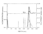
FIG. 2. Dynamic SIMS (secondary ion mass spectroscopy) data for a copper film pretreated with a hydrogen (H2) plasma, then exposed to 20 seconds of 9% Me4Sn in helium, post treated with a H2 plasma then capped with 400 nm of PECVD (Plasma Enhanced Chemical Vapor Deposition) Si3N4
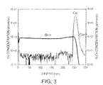
FIG. 3. Dynamic SIMS (secondary ion mass spectroscopy) data for a copper film pretreated with a hydrogen (H2) plasma, then exposed to 20 seconds of CpCo(CO)2, post treated with hydrogen (H2) plasma then capped with 400 nm of PECVD Si3N4.
FIG. 4. Dynamic SIMS (secondary ion mass spectroscopy) data for a copper film pretreated with a hydrogen (H2) plasma, then exposed to 20 seconds of CpMn(CO)3, post treated with a hydrogen (H2) plasma then capped with 400 nm of PECVD Si3N4.
FIG. 5. Dynamic SIMS (secondary ion mass spectroscopy) data for a copper film pretreated with a hydrogen (H2) plasma, then exposed to 20 seconds of EtCp2Ni, post treated with a hydrogen (H2) plasma then capped with 400 nm of PECVD Si3N4.
FIG. 6. X-ray photoelectron spectroscopy (XPS) data for the amount of tin at the copper surface presented as a ratio of Sn/Cu (%).
DETAILED DESCRIPTION OF THE INVENTION
Copper adhesion to barrier layers and electromigration resistance are extremely important properties affecting device yield and device lifetimes. Currently the microelectronics industry is evaluating both silane exposure and electroless cobalt deposition to improve adhesion between the copper and the barrier dielectric layer. These are not optimal solutions as the silane treatments increase the copper resistivity which is a significant concern at the 32 nm generation and below, and the electroless cobalt deposition requires significant added steps to integrate.
The deposition of oxygen containing films directly onto copper generally does not result in highly adhesive interfaces due to the formation of copper oxide. Therefore dielectric barrier materials reported in the literature are generally silicon nitride or organosilicon carbonitride based materials, however, there is a desire in the microeletronics industry to use silicon oxide, organosilicon oxycarbide, organosilicon oxynitride, organosilicon carbonitride or organosilicon oxycarbonitride based films as barrier dielectrics because of their reduced dielectric constants. The method described in the present invention, that is, the use of certain volatile metallic materials as the adhesion promoter may allow for the deposition of oxygen-containing barrier films onto copper layers while retaining excellent adhesion properties. Metals under consideration are zinc, silver, chromium, tin, manganese, nickel, aluminum, and cobalt.
The organometallic precursor is selected from the group consisting of Tetramethyltin (Me4Sn), dibutyldimethyltin, tributyltin hydride, tin hydride (SnH4) and tin deuteride (SnD4), Tetraalkyltin, trialkyltin hydride, dialkyltin dihydride, Alkylalkoxytin, Tetraalkoxytin, tetrakis(dialkylamino)tin, cyclopentadienyl cobalt dicarbonyl (CpCo(CO)2), nitrosyl cobalt pentacarbonyl, cyclopentadienyl manganese tricarbonyl (CpMn(CO)3), bis(ethylcyclopentadienyl)nickel ((EtCp)2Ni), Diethylzinc (Et2Zn), Diethylzinc-Trimethylamine adduct, Dimethylzinc, Dialkylzinc, amine adducts of Dialkylzinc, Nickel hexacarbonyl (Ni(CO)6), Tungsten hexafluoride (WF6), Chromium hexacarbonyl (Cr(CO)6), trimethylaluminum, dimethylethylamine alane (DMEAA), and Tungsten hexacarbonyl (W(CO)6).
A delivery apparatus for the organometallic precursors in the present invention includes any container designed for safety delivery. A typical container comprises an interior volume bounded by interior wall, an inlet, and an outlet.
The specific pressurized apparatus and method disclosed in U.S. Pat. No. 7,013,916 can also be used in the present invention. The entire disclosure of this United States patent is hereby incorporated by reference into this specification.
The organometallic precursor can be contained and delivered at sub-atmospheric pressure in a pressurized container, which includes
  • (a) a valve body in sealed communication with an outlet orifice of the pressurized container, said outlet orifice of said pressurized container open to an interior chamber of said pressurized container;
  • (b) a fluid discharge path in the valve body, between the outlet orifice of the pressurized container and an outlet orifice of the valve body;
  • (c) a pressure regulator having a pressure sensing means capable of responding to sub-atmospheric pressure, integral to said valve body, in-line in the fluid discharge path, said pressure regulator pre-set to a pressure below atmospheric pressure to allow said gas to be delivered through said regulator from said interior chamber only when said pressure sensing means senses a downstream pressure at or below said pre-set pressure; and
  • (d) a high pressure shut-off valve integral to said valve body, in-line in the fluid discharge path and upstream from said pressure regulator; whereby said gas may flow through from said interior chamber of said pressurized container through said fluid discharge path, through said outlet orifice of said pressurized container, and through said outlet orifice of said valve body only when said outlet orifice is connected to a vacuum system.
The deposition process used in the present invention can be any known process such as, Atomic Layer Deposition (ALD), Atomic Layer Treatment (ALT), Plasma Enhanced Atomic Layer Deposition (PEALD), Chemical Vapor Deposition(CVD), and Plasma Enhanced Chemical Vapor Deposition(PECVD), Low Pressure Chemical Vapor Deposition(LPCVD), Sub Atmospheric Chemical Vapor Deposition(SACVD), UV-assisted Chemical Vapor Deposition, Filament-assisted Chemical Vapor Deposition (FACVD), and Atmospheric Pressure Chemical Vapor Deposition (APCVD).
In the fabrication process, a direct liquid injection (DLI) delivery method can be employed. The precursor can be delivered by DLI of either a pure liquid precursor or by DLI of a mixture of the precursor with a solvent in a vessel or a container that is designed for the deposition delivery. A typical container comprises an interior volume bounded by interior wall, an inlet, and an outlet.
Organometallic precursors are vaporized either in the pure form or as mixtures, and the resulting precursor vapor, typically mixed with a carrier gas (such as argon, helium or nitrogen) is transported to a reactor, for example, a chemical vapor deposition (CVD) reactor.
More specifically, the organometallic precursor can comprise a solvent which solubilizes the organometallic precursor without decomposing it. The weight % of the solvent can be ranging from 5% to 99%; preferably 50% to 90%.
Suitable solvents can be the simple hydrocarbons of the basic formula CnH(2n+2−x); where n is 3-10 and x is equal to the number of cyclic structures or the degrees of unsaturation; for example, hexane, hexadiene, pentane, heptane, cyclohexane, cyclooctane or an aromatic hydrocarbon of the general structure C6H(6−b)Rb where R can be 0-6 and can be the same or different, for example toluene, mesytelene, xylene, para-cymene and combinations thereof.
Some organometallic precursors may also be soluble in oxygen containing solvents such as ethers, for example diethyl ether, methyl isobutyl ether, or tetrahydrofuran, alcohols, for example methanol, ethanol, or isopropanol, ketones for example acetone, aldehydes, or esters.
Some of the advantages which may be available through the use of these solutions include the following:
lowering the flammability of the mixture by choosing a solvent with a flammability lower than the organometallic;
ability to delivery small amounts of organometallic precursor to the chamber using a dilute mixture;
lowering the concentration of a potentially toxic organometallic precursor by dilution;
an ability to tune the physical properties of the precursor solution such as viscosity for easy and safe delivery.
The deposition of oxygen containing films directly onto copper generally does not result in highly adhesive interfaces due to the formation of copper oxide. Therefore dielectric barrier materials reported in the literature are generally silicon nitride or organosilicon carbonitride based materials, however, there is a desire in the microeletronics industry to use silicon oxide, organosilicon oxycarbide, organosilicon oxynitride, organosilicon carbonitride or organosilicon oxycarbonitride based films as barrier dielectrics because of their reduced dielectric constants. The method described in the present invention, that is, the use of certain metallic materials, such as tin or zinc, as the adhesion promoter may allow for the deposition of oxygen-containing barrier films onto copper layers while retaining excellent adhesion properties. The dielectric barrier layer materials such as silicon nitride, silicon oxide, silicon carbide, silicon oxycarbide, silicon oxynitride, silicon carbonitride, silicon oxycarbonitride and mixtures are considered, where the “silicon” includes “organosilicon”. For example, the list of materials includes organosilicon oxycarbide, organosilicon oxynitride, organosilicon carbonitride, organosilicon oxycarbonitride and mixtures. The barrier layer has a dielectric constant of less than 7. An example of dielectric barrier layer material is a Si3N4.
A consideration here is that the metal or the organometallic precursor should not negatively impact the dielectric materials exposed to the same processing. Examples of dielectric materials include silicon dioxide, fluorosilicate glass (FSG), organosilicate glass (OSG), aka carbon doped oxide (CDO), or porous low-k dielectric materials. Examples of low k dielectric materials used in the integration scheme include porous OSG (organosilicate glass) materials such as those deposited from PDEMS™ interlayer dielectric (ILD) deposition process. The low k dielectric materials usually have a dielectric constant of less than 3.0. The dielectric material has a dielectric constant of less than 3.2.
With the materials considered above together, a structure having improved conductive metal adhesion to a barrier layer and electromigration resistance is formed in the present invention. The structure comprises:
    • (a) at least one patterned dielectric layer with embedded conductive metal features(such as copper or copper alloys);
    • (b) an adhesion layer selectively deposited at least on the conductive metal features, said adhesion layer is selected from the group consisting of tin and zinc;
    • (c) a dielectric barrier layer covering the at least one patterned dielectric layer with embedded conductive metal features having the adhesion layer.
The structure can further have a metal barrier layer formed between the patterned dielectric layer and the embedded conductive metal features. The metal barrier layer comprises materials such as tantalum, tantalum nitride, titanium, titanium nitride, cobalt, rhuthenium, and other advanced barrier materials which prevent diffusion of the copper into the dielectric material.
WORKING EXAMPLES
The following examples are provided for the purpose of further illustrating the present invention but are by no means intended to limit the same.
In the following examples, film treatments were carried out on an Applied Materials Precision-5000 system equipped to process 200 mm silicon wafers. Thermal treatments were carried out in a D×L vacuum chamber, organometallic precursors were delivered to the chamber either by vapor draw or entrained with helium as a carrier gas. Plasma treatments and deposition of silicon nitride films were carried out in a D×L vacuum chamber that was fitted with an Advance Energy 200 rf generator. Adhesive energies were measured via 4-point bend using a DTS Company Delaminator instrument. Bulk film resistivity was measured on 100 nm thick copper films using a 4-point probe.
Silicon nitride cap layers were deposited using a standard Si3N4 deposition recipe: 100 sccm NH3, 75 sccm SiH4, 2000 sccm N2, 3.5 torr chamber pressure, 400 mili-inch susceptor to wafer spacing, 300° C. wafer temperature, and 300 W power.
Organometallic precursors evaluated were tretramethyltin (Me4Sn), cyclopentadienyl cobalt dicarbonyl (CpCo(CO)2), cyclopentadienyl manganese tricarbonyl (CpMn(CO)3), and bis(ethyl-cyclopentadienyl) nickel ((EtCp)2Ni).
Adhesion measurements are widely viewed as an acceptable surrogate measurement to predict performance in promoting electromigration resistance. Adhesion values were measured for copper films treated with various processes and capped with 400 nm of PEVCD Si3N4. 4-Point bend measurements were made by gluing a piece of silicon wafer on top of the Si3N4 film with epoxy, notching the top silicon wafer and using standard 4-point bend techniques. For examples 1 and 7 a 15 nm thick layer of chromium followed by a 150 nm thick layer of aluminum were deposited by sputtering onto both the silicon wafer and the Si3N4 in order to improve the adhesion strength of the epoxy.
In order to determine the adhesion value without any copper treatment a 400 nm thick layer of Si3N4 was deposited on top of a copper film that had not been treated, these films failed at the Si3N4/copper interface with a value of 4.0+/−0.5 J/m2.
Example 1 Exposure of a Copper film to H2 Plasma Pre-treatment
A series of films were exposed to 30 second hydrogen plasma to examine a baseline process for copper film pretreatment. In order to investigate the effect of a H2 plasma on adhesion, a copper film was treated with a 30 second H2 plasma followed by deposition of 400 nm of PECVD Si3N4.
Measurement of the adhesion with the 4-point bend technique revealed an adhesion value of 12.5 J/m2.
To examine the impact of a H2 plasma on the bulk resistivity of a copper film a 100 nm thick copper film with a bulk resistivity of 0.22 ohm-cm as measured by 4-point probe was exposed to a H2 plasma for 30 seconds after which time the bulk resistivity was measured as 0.19 ohm-cm, this decrease is presumably due to the reduction of a thin copper oxide layer on top of the copper.
The data was summarized in Tables I and II.
Example 2 Exposure of a Porous OSG (Organosilicate Glass) (PDEMS™) to H2 Plasma Pre-treatment
In order to investigate the effect of a H2 plasma on a porous organosilicate glass (OSG), a porous OSG PDEMS films were deposited by flowing a blend of diethoxymethylsilane (DEMS) and alpha terpinene into a vacuum chamber, striking a plasma to co-deposit an organosilicate glass (OSG) and a sacrificial organic porogen. This film is then annealed in using ultraviolet light to remove the sacrificial porogen to yield a porous OSG.
The porous OSG PDEMS films were then exposed to a 30 second H2 plasma, this resulted in a increase in the dielectric constant from 2.2 to 2.4, a increase in leakage current from 8 pico-amperes to 168 pico-amperes, and a minor change in breakdown voltage from ˜4 to 3.75 MV/m.
The data was summarized in Table III.
Example 3 Exposure of a copper film to H2 plasma Pre-treatment, SiH4 in nitrogen and NH3 plasma post-treatment
A series of films were exposed to a 30 second hydrogen plasma pre-treatment, followed by exposure to a mixture of 5% SiH4 in nitrogen at 4.5 torr for a variable amount of time, and finally to a NH3 plasma for 30 seconds post-treatment as shown below, in order to examine a baseline process for copper treatment.
  • 1) H2 plasma pre-treat to reduce CuO
    • 300 sccm H2, 2.7 torr, 400 mil spacing, 3000° C., at 300 W for 30 seconds
  • 2) SiH4 exposure
    • 2000 sccm N2, 100 sccm SiH4, 4.5 Torr, 300° C. for a variable length of time
  • 3) NH3 plasma post treatment
    • 200 sccm NH3, 4.5 Torr, 300 mil, 3000° C., at 300 W for 30 seconds
  • 4) This may or may not have been followed with a Si3N4 capping layer.
To examine the impact of the silane treatment on the bulk resistivity of a copper film a 100 nm thick copper film with a bulk resistivity of 0.21 ohm-cm as measured by 4-point probe was exposed to the silane treatment for 5 and 10 seconds with H2 plasma pre treatment and a NH3 plasma post treatment after which time the bulk resistivity was measured as 0.40 and 0.47 ohm-cm respectively. This sharp increase is believed to be due to silicon diffusing into the copper.
Similar samples with a thicker copper film were prepared and submitted for dynamic SIMS (secondary ion mass spectroscopy), the results of this analysis as well as that for a standard copper film exposed only to H2 plasma treatment are shown in FIG. 1, it is evident that as the silane exposure times increased the amount of and depth of silicon diffusion also increased.
The data was summarized in Table II.
Example 4 Exposure of a Copper Film to H2 Plasma Pre-treatment, tetremethyltin(Me4Sn), Without Post Exposure Treatment
Measurement of the adhesion between a copper film which had been exposed to a H2 plasma pre-treatment, followed by a 10 second exposure to an organometallic precursor: 9% Me4Sn in He at 4.5 Torr and 300° C. then capped with a 400 nm film of PECVD Si3N4 was measured with the 4-point bend technique which yielding an adhesion value of 6.3+/−1 J/m2 with delamination occurring at the copper/Si3N4 interface. This indicates no improvement in adhesion relative to the untreated copper film. The data was summarized in Table I.
Example 5 Exposure of a Porous OSG to Tetremethyltin(Me4Sn)
In order to investigate the effect of a Me4Sn exposure on a porous organosilicate glass (OSG), the porous OSG deposited as described in Example 2 was exposed to an organometallic precursor: 9% mixture of Me4Sn in helium at 3000° C. for 20 seconds, this resulted in a increase in the dielectric constant from 2.2 to 2.3, a minor change in leakage current from ˜8 pico-amperes to 7 pico-amperes, and a minor change in breakdown voltage from ˜4 to 4.18 MV/m.
The last measurement was also repeated for the exposure to Me4Sn after a 30 second H2 plasma treatment.
Compared to the values measured above for a porous OSG PDEMS™ film exposed just to a H2 plasma treatment (Example 2), further exposure to 20 seconds of Me4Sn resulted in a minor change in the dielectric constant from 2.5 to 2.4, a minor change in leakage current from 166 pico-amperes to 230 pico-amperes, and a minor change in breakdown voltage from 3.76 to 3.62 MV/m. The data was summarized in Table III.
Example 6 Exposure of a Copper Film to H2 Plasma Pre-treatment, tetremethyltin (Me4Sn) and H2 Plasma Post-treatment
Measurement of the adhesion between a sample which had been exposed to a H2 plasma followed by a 10 second exposure to 9% Me4Sn in He then treated with a H2 plasma post treatment and capped with a 400 nm film of PECVD Si3N4 was measured with the 4-point bend technique described previously which yielded an adhesion value of 22.0 J/m2. The delamination occurred at the copper/Si3N4 interface.
To examine the impact of the this Me4Sn treatment on the bulk resistivity of a copper film 100 nm thick copper films with bulk resistivities of 0.22 and 0.20 ohm-cm as measured by 4-point probe were exposed to the Me4Sn treatment for 10 and 20 seconds with H2 plasma pre and post treatments after which time the bulk resistivity was measured as 0.18 and 0.17 ohm-cm respectively, this decrease in resistivity is believe to be due to a combination of (1) reduction of the CuO layer with the H2 plasma pretreatment and (2) a relatively low resistivity of the thin adhesion layer deposited by the Me4Sn.
The data was summarized in Table I and II.
Similar samples with a thicker copper film were prepared and submitted for dynamic SIMS (secondary ion mass spectroscopy), these films were treated with a 20 second exposure to 9% Me4Sn in helium with pre and post H2 plasma treatments then capped with a 400 nm thick PECVD Si3N4 layer.
The result of the analysis is shown in FIG. 2. It is evident that the Me4Sn exposure results in the deposition of a thin tin containing layer at the interface between the copper and the Si3N4.
A set of wafers were obtained on which patterned Black Diamond™ organosilicate glass films were filled with copper metal, these patterned features included Kelvin structures of varying line widths (0.14-0.18 microns) to measure copper line resistance and comb-serpintene structures (0.16×0.18 microns) to evaluate leakage current and electrical shorting. These wafers were first treated with a hydrogen plasma at 350 C for 20 seconds to reduce the surface copper oxide, these were then exposed to tetramethyl tin for 30 seconds at 350 C followed by a second hydrogen plasma to remove residual carbon from the surface. These wafers were then electrically probed to test for leakage current and electrical shorts as well as measuring copper line resistance. Testing of the Kelvin structures revealed that the copper line resistance was not increased by treatment with tetramethyl tin which indicates that the treatment with tetramethyl tin results in only a surface treatment, if the tin had diffused into the copper an increase in copper resistance would have been observed. Testing of the Comb-Serpentine structures revealed that the treatment with tetramethyl tin does not increase the line to line leakage current and no electrical shorts were observed indicating that the tetramethyl tin treatment does not deposit a conductive layer of tin on the Organosilicate Glass supporting the fact of selective treatment of the copper surface with tetramethyl tin. Additionally there was no increase in capacitance between metals lines which indicates that the tetramethyl tin treatment does not damage the organosilicate glass.
Example 7 Exposure of a Copper Film to H2 Plasma Pre-treatment, Cyclopentadienyl Cobalt Dicarbonyl (CpCo(CO)2) and H2 Plasma Post-treatment
Measurement of the adhesion between a sample which had been exposed to a H2 plasma followed by a 10 second exposure to vapors of CpCo(CO)2 at 3000° C. then treated with a H2 plasma post treatment and capped with a 400 nm film of PECVD Si3N4 was measured with the 4-point bend technique yielding an adhesion value of 17.5 J/m2, however, the delamination occurred between the top of the Si3N4 and the bare silicon used in the 4-point bend technique, therefore the adhesion strength of the copper/Si3N4 interface could not be unambiguously measured.
The data was summarized in Table I.
Similar samples with a copper film exposed to the cobalt treatment were prepared and submitted for dynamic SIMS (secondary ion mass spectroscopy), these films were treated with a 20 second exposure to CpCo(CO)2 vapors at 3000° C. with pre and post H2 plasma treatments then capped with a 400 nm thick PECVD Si3N4 layer. The result of the analysis is shown in FIG. 3. It is evident that the CpCo(CO)2 exposure results in the deposition of a thin cobalt containing layer at the interface between the copper and the Si3N4.
Example 8 Exposure of a Copper Film to H2 Plasma Pre-treatment, Cyclopentadienyl Manganese Triicarbonyl (CpMn(CO)3) and H2 Plasma Post-treatment
Measurement of the adhesion between a sample which had been exposed to a H2 plasma followed by a 10 second exposure to vapors of CpMn(CO)3 at 3000° C. then treated with a H2 plasma post treatment and capped with a 400 nm film of PECVD Si3N4 was measured with the 4-point bend technique yielding an adhesion value of 21.9+/−2.3 J/m2, however, the delamination occurred between the top of the Si3N4 and the bare silicon used in the 4-point bend technique, therefore the adhesion strength of the copper/Si3N4 interface could not be unambiguously measured. The data was summarized in Table I.
Similar samples with a copper film exposed to the manganese treatment were prepared and submitted for dynamic SIMS (secondary ion mass spectroscopy), these films were treated with a 20 second exposure to CpMn(CO)3 vapors at 3000° C. with pre and post H2 plasma treatments then capped with a 400 nm thick PECVD Si3N4 layer.
The result of the analysis is shown in FIG. 4. It is evident that the CpMn(CO)3 exposure results in the deposition of a thin manganese containing layer at the interface between the copper and the Si3N4.
Example 9 Exposure of a Copper Film to H2 Plasma Pre-treatment, Bis(ethylcyclopentadienyl)Nickel (EtCp2Ni) with H2 Plasma Post-treatment
Measurement of the adhesion between a sample which had been exposed to a H2 plasma followed by a 10 second exposure to vapors of EtCp2Ni at 300° C. then treated with a H2 plasma post treatment and capped with a 400 nm film of PECVD Si3N4 was measured with the 4-point bend technique yielding an adhesion value of 31.5 J/m2, however, the delamination occurred between the top of the Si3N4 and the bare silicon used in the 4-point bend technique, therefore the adhesion strength of the copper/Si3N4 interface could not be unambiguously measured.
The data was summarized in Table I.
Similar samples with a copper film exposed to the manganese treatment were prepared and submitted for dynamic SIMS (secondary ion mass spectroscopy), these films were treated with a 20 second exposure to EtCp2Ni vapors at 3000° C. with pre and post H2 plasma treatments then capped with a 400 nm thick PECVD Si3N4 layer.
The result of the analysis is shown in FIG. 5. It is evident that the EtCp2Ni exposure results in the deposition of a thin nickel containing layer at the interface between the copper and the Si3N4.
The data from above measurements are summarized in Table I.
TABLE I
Effect of Process on Adhesion between
PECVD Si3N4 and Copper
Process Adhesion (J/m2)
Untreated Film   4 +/− 0.5
H2 Treatment 12.5
Me4Sn with out Post 6.3 +/− 1.0
20 second Me4Sn with H2 Post 22.0
CpMn(CO)3 with H2 Post 21.9 +/− 2.3 
(EtCp)2Ni with H2 post 31.5
CpCo(CO)2 with H2 post 17.5
Table I shows the effect of various processes on the adhesion between the copper layer and the capping PECVD deposited Si3N4. These measurements were carried out by the industry standard 4-point bend technique. Unless otherwise noted all films were pretreated with a hydrogen plasma.
The untreated copper film shows a low adhesion value of 4+/0.5 J/m2 with delamination at the Si3N4 to copper interface due to the poor adhesion to the native oxide found on copper films. Treatment with hydrogen plasma will reduce the copper oxide back to copper metal and an adhesion value of 12.5 J/m2 is measured with failure observed between the Si3N4 and the copper interface.
Treatment of the copper with a hydrogen plasma followed by a 10 second exposure to Me4Sn with no post treatment followed by capping with a PECVD Si3N4 layer results in an adhesion value of 6.3 J/m2 with delamination at the Si3N4 to copper interface which is believed to be due to residual carbon at the surface after treatment with the Me4Sn. Treatment with hydrogen plasma after exposure the Me4Sn improves adhesion dramatically and an adhesion value of 22.0 J/m2 is observed with delamination occurring at the Si3N4/copper interface. Copper films treated with cyclopentadienylmanganese tricarbonyl, bis(ethylcyclopentadienyl)nickel, and cyclopentadienylcobalt dicarbonyl vapors followed by a hydrogen plasma treatment were not examined with the advanced 4-point bend technique in which chromium and aluminum layer deposition and thus delamination occurred at the epoxy interface which indicates good adhesion although accurate measurements were not possible.
TABLE II
Effect of copper treatments on bulk copper resistivity
Resistivity Resistivity Change in
before treatment after treatment resistivity
Treatment (10−3 ohm-cm) (10−3 ohm-cm) (%)
H2 plasma only 224 +/− 4 186 +/− 4 −17
NH3 plasma only 182 +/− 2 167 +/− 2 −8
H2 plasma/5 second 214 +/− 4  402 +/− 30 89
SiH4/NH3 plasma
H2 plasma/10 second 210 +/− 4  466 +/− 26 122
SiH4/NH3 plasma
H2 plasma/10 second 221 +/− 4 185 +/− 1 −16
Me4Sn/H2 plasma
H2 plasma/20 second 200 +/− 8 174 +/− 6 −13
Me4Sn/H2 plasma
Table II shows the effect of various copper treatments on the bulk resistivity of a 100 nm thick copper film as measured by 4-point probe before and after treatment. All treatments were carried out at 300° C. Exposure of the copper films to just hydrogen or ammonia plasmas lower the bulk resistivity by 8 to 17% presumably due to reduction of the native copper oxide layer found on top of the untreated films. Exposure of the copper to either 5 or 10 seconds of SiH4 in the “standard silane process” results in significant bulk resistivity increases of 89 and 122% respectively, presumably due to formation of CuSiN and diffusion of Si into the bulk of the copper. Exposure of the copper layer to Me4Sn for either 10 or 20 seconds with pre and post hydrogen plasma treatments results in decrease the bulk resistivity by 16 and 13% respectively. These changes are similar to those measured for just hydrogen plasma only treatments, which indicates that the layer which is deposited from the Me4Sn exposure does not significantly impact the copper resistivity as is seen with silane exposure.
TABLE III
Effect of Me4Sn treatment on porous OSG films (PDEMS ™)
Dielectric Leakage Breakdown
Treatment Constant Current (pA) Voltage (MV/m)
Untreated ~2.2 ~8 ~4
10 second Me4Sn 2.28 7 4.18
H2 plasma only 2.46 166 3.75
H2 plasma/10 second 2.44 137 3.62
Me4Sn
H2 plasma/20 second 2.44 230 3.62
Me4Sn
Table III shows the effect of Me4Sn on the electrical performance of porous organosilicate films such as those produced by PDEMS™ ILD deposition process with a dielectric constant of ˜2.2. This experiment was performed to determine if the Me4Sn would diffuse into the pores of a porous OSG potentially degrading the electrical performance of the porous OSG. A PDEMS™ film with a measured dielectric constant of ˜2.2 was exposed to Me4Sn for 10 seconds at 300° C. The dielectric constant, leakage current and breakdown voltages are either unaffected or only minimally effected by exposure to the Me4Sn. These measurements were also run after exposure of the PDEMS™ to a hydrogen plasma and the values are given, the hydrogen plasma results in a increase in dielectric constant and leakage current. Exposure of the hydrogen plasma treated films to Me4Sn for 10 and 20 seconds does not significantly affect the dielectric constant or breakdown voltage. There is a measured difference in leakage current upon exposure to the Me4Sn, however, we do not believe that the measured differences are significant.
Example 10 Measurement of Tin Deposited on the Copper Film
This example repeated the same measurement as set in Example 7, but with various exposure times and temperatures.
Samples of copper films were first in-situ plasma treated with a H2 plasma to reduce the surface copper oxide (pre-treatment), after which the samples were exposed to tetremethyltin (Me4Sn) as a 9% mixture in helium for various exposure times and temperatures. The samples were once again exposed to a H2 plasma to remove surface carbon (post-treatment). Samples were then submitted for surface X-ray photoelectron spectroscopy (XPS) analysis to measure the Tin on the copper films. The percent tin was measured as a ratio relative to copper.
Table IV shows that for all exposures only a small amount of tin was deposited, if it is assumed that a monolayer of tin would be result in a XPS signal of 5 atomic % these samples have slightly less than a monolayer of tin on the surface. The observation that a film exposed for 20 seconds and a film exposed for 80 seconds had essentially the same level of tin indicates that this is a surface limited reaction and not a continual deposition reaction. This is further indicated by the samples which was exposed at 350 C which also showed essentially the same level of tin indicating that the deposition is not thermally driven.
TABLE IV
Process % Sn/Cu by XPS
20 second exposure 1.4
to Me4Sn at 300 C.
80 second exposure 0.8
to Me4Sn at 300 C.
20 second exposure 1.1
to Me4Sn at 350
Next, three samples of copper films were first treated with a H2 plasma, then exposed to Me4Sn for 20 seconds followed by a H2 plasma. The above whole process was repeated 5 times and 10 times respectively on two of the three samples. The samples were then submitted for surface X-ray photoelectron spectroscopy (XPS) analysis to measure the tin on the copper surface. The percent tin was measured as a ration relative to copper.
As shown in FIG. 6, the amount of tin increased from 1.4%, to 2.0% and finally 3.4% for one, five and ten process cycles, respectively. The whole process can be repeated until a desired thickness of the tin on the copper surface is achieved. This indicates that the ALD process can also be used to deposit tin onto the copper surface.
Samples of wafers with PDEMS and Si3N4 films on them were exposed to the same process described above for five cycles. Then, the sample was submitted for surface X-ray photoelectron spectroscopy (XPS) analysis to measure the Tin on the surfaces of PDEMS and Si3N4 films. There was no tin observed above the detection limit of the XPS, indicating that the Me4Sn process is a selective deposition process.
Example 11 Exposure of a Copper Film to H2 Plasma Pre-treatment, Tetramethyl Tin/Anhydrous Hexane Mixture with NH3 Plasma Post-treatment
A mixture of 5 mL tetramethyl tin along with 95 mL anhydrous hexane was prepared in a drybox. This mixture was then delivered to the CVD chamber by means of direct liquid injection of the mixture with a vaporization temperature of 50° C.
Copper films were first treated with a H2 plasma to reduce the copper oxide followed by exposure of the film to vapors of the tetramethyl tin/hexane mixture at 350° C. for 30 seconds after which time the films were post-treated with a NH3 plasma and finally coated with a Silicon carbon nitride film.
Analysis of the resulting film stack by x-ray photoelectron spectroscopy shows a clean metallic tin layer at the copper/silicon carbonitride interface. The use of a solvent such as hexane which does not influence the tin treatment offers advantages in safety and handling.
The foregoing examples and description of the preferred embodiments should be taken as illustrating, rather than as limiting the present invention as defined by the claims. As will be readily appreciated, numerous variations and combinations of the features set forth above can be utilized without departing from the present invention as set forth in the claims. Such variations are not regarded as a departure from the spirit and scope of the invention, and all such variations are intended to be included within the scope of the following claims.

Claims (36)

1. A method for improving adhesion of a semiconductor device comprising steps of:
(a) providing a substrate in a processing chamber;
wherein the substrate comprises at least one patterned dielectric layer and at least one patterned conductive metal layer;
(ab) exposing the substrate to a pre-treatment; and
(b) introducing an organometallic precursor to the processing chamber to selectively deposit an adhesion layer on the at least one patterned conductive metal layer;
wherein
the organometallic precursor is selected from the group consisting of organozinc, organosilver, organochromium, organotin, organomanganese, organonickel, organocobalt , organoaluminum, and mixtures thereof; and
steps (ab) and (b) are repeated until a desired thickness of the adhesion layer is achieved.
2. The method in claim 1, wherein the pre-treatment is selected from the group consisting of H2 plasma, NH3 plasma, H2/He plasma, H2/N2 plasma and mixtures thereof.
3. The method in claim 1 further comprising a step (c) depositing a dielectric barrier layer on the substrate having the adhesion layer.
4. The method in claim 3 further comprising a step before (c):
exposing the substrate having the adhesion layer to a post-treatment.
5. The method in claim 3, wherein the dielectric barrier layer is selected from the group consisting of: silicon nitride, silicon oxide, silicon oxycarbide, silicon oxynitride, silicon carbonitride, silicon oxycarbonitride, silicon carbide, and mixtures thereof.
6. The method of claim 3 wherein the dielectric barrier layer has a dielectric constant of less than 7.
7. The method in claim 4, wherein the post-treatment is selected from the group consisting of H2 plasma, NH3 plasma, H2/He plasma , H2/N2 plasma and mixtures thereof.
8. The method in claim 1, wherein the organometallic precursor is solubilized in a solvent selected from the group consisting of a hydrocarbon with formula CnH(2n+2−x); where n is 3-10 and x is equal to the number of cyclic structures or the degrees of unsaturation; an oxygen containing solvents; and mixtures thereof;
wherein the solvent solubilizes the organometallic precursor without decomposing the organometallic precursor.
9. The method in claim 8, wherein weight % of the solvent ranges from 5% to 99%.
10. The method in claim 8, wherein weight % of the solvent ranges from 50% to 90%.
11. The method in claim 8, wherein the oxygen containing solvent is selected from the group consisting of an ester, an alcohol, and mixtures thereof.
12. The method in claim 8, wherein the hydrocarbon is selected from the group consisting of hexane, hexadiene, pentane, heptane, cyclohexane, cyclooctane, an aromatic hydrocarbon of the general structure C6H(6−b)Rb, wherein R is 0-6, and mixtures thereof.
13. The method in claim 12, wherein the aromatic hydrocarbon is selected from the group consisting of toluene, mesytelene, xylene, para-cymene and mixtures thereof.
14. The method in claim 1, wherein the organometallic precursor is contained and delivered in a container comprising an interior volume bounded by interior wall, an inlet, and an outlet.
15. The method in claim 1, wherein the organometallic precursor is contained and delivered at sub-atmospheric pressure in a pressurized container, comprising
(a) a valve body in sealed communication with an outlet orifice of the pressurized container, said outlet orifice of said pressurized container open to an interior chamber of said pressurized container;
(b) a fluid discharge path in the valve body, between the outlet orifice of the pressurized container and an outlet orifice of the valve body;
(c) a pressure regulator having a pressure sensing means capable of responding to sub-atmospheric pressure, integral to said valve body, in-line in the fluid discharge path, said pressure regulator pre-set to a pressure below atmospheric pressure to allow said gas to be delivered through said regulator from said interior chamber only when said pressure sensing means senses a downstream pressure at or below said pre-set pressure; and
(d) a high pressure shut-off valve integral to said valve body, in-line in the fluid discharge path and upstream from said pressure regulator; whereby said gas may flow through from said interior chamber of said pressurized container through said fluid discharge path, through said outlet orifice of said pressurized container, and through said outlet orifice of said valve body only when said outlet orifice is connected to a vacuum system.
16. The method of claim 1 wherein the at least one patterned dielectric layer is selected from the group consisting of silicon dioxide, fluorosilicate glass (FSG), organosilicate glass (OSG), carbon doped oxide (CDO), a porous organosilicate glass having a dielectric constant of less than 3.0, and mixtures thereof.
17. The method of claim 1 wherein the at least one patterned dielectric layer has a dielectric constant of less than 3.2.
18. The method in claim 1, wherein the at least one patterned conductive metal layer is selected from the group consisting of copper, copper alloys and mixtures thereof.
19. The method in claim 1, wherein the organometallic precursor is selected from the group consisting of tetramethyltin (Me4Sn), dibutyldimethyltin, tributyltin hydride, tetraalkyltin, trialkyltin hydride, dialkyltin dihydride, alkylalkoxytin, tetraalkoxytin, tetrakis(dialkylamino)tin, tin hydride (SnH4), tin deuteride (SnD4), cyclopentadienyl cobalt dicarbonyl (CpCo(CO)2), nitrosyl cobalt pentacarbonyl, cyclopentadienyl manganese tricarbonyl (CpMn(CO)3), bis(ethylcyclopentadienyl)nickel ((EtCp)2Ni), diethylzinc (Et2Zn), diethylzinc-trimethylamine adduct, dimethylzinc, dialkylzinc, amine adducts of dialkylzinc, nickel hexacarbonyl (Ni(CO)6), tungsten hexafluoride (WF6), chromium hexacarbonyl (Cr(CO)6), trimethylaluminum, dimethylethylamine alane (DMEAA) , tungsten hexacarbonyl (W(CO)6), and mixtures thereof.
20. The method in claim 1, wherein the adhesion layer is deposed by a process selected from the group consisting of Atomic Layer Deposition (ALD), Plasma Enhanced Atomic Layer Deposition (PEALD), Chemical Vapor Deposition(CVD), and Plasma Enhanced Chemical Vapor Deposition(PECVD), Low Pressure Chemical Vapor Deposition(LPCVD), Sub Atmospheric Chemical Vapor Deposition(SACVD), UV-assisted Chemical Vapor Deposition, Filament-assisted Chemical Vapor Deposition (FACVD), and Atmospheric Pressure Chemical Vapor Deposition (APCVD).
21. The method in claim 1, wherein the adhesion layer is selected from the group consisting of tin and zinc.
22. The method of claim 1, wherein the adhesion layer is tin.
23. A method for processing a semiconductor device having an improved adhesion comprising steps of:
(a) providing a substrate in a processing chamber;
wherein the substrate comprises at least one patterned dielectric layer and at least one patterned conductive metal layer;
(b exposing the substrate to a pre-treatment;
(c) introducing an organotin precursor to the processing chamber to selectively deposit an adhesion layer on the at least one patterned conductive metal layer after the pre-treatment in (b);
(d) exposing the substrate having the adhesion layer to a post-treatment; and
(e) depositing a dielectric barrier layer on the substrate having the adhesion layer after the post-treatment in (d).
24. The method in claim 23, wherein steps (b), (c) and (d) are repeated until a desired thickness of the adhesion layer is achieved.
25. The method in claim 23, wherein
the at least one patterned dielectric layer is selected from the group consisting of silicon dioxide, fluorosilicate galss (FSG), organosilicate glass (OSG), carbon doped oxide (CDO), a porous organosilicate glass having a dielectric constant of less than 3.0, and mixtures thereof;
the at least one patterned conductive metal layer is selected from the group consisting of copper , copper alloys, and mixtures thereof;
the pre-treatment and the post-treatment are both H2 plasma; and
the organotin precursor is selected from the group consisting of Tetramethyltin (Me4Sn), dibutyldimethyltin, tributyltin hydride, tetraalkyltin, trialkyltin hydride, dialkyltin dihydride, alkylalkoxytin, tetraalkoxytin, tetrakis(dialkylamino)tin, tin hydride (SnH4), tin deuteride (SnD4), and mixtures thereof.
26. The method in claim 23, wherein the organotin precursor is Tetramethyltin (Me4Sn).
27. The method in claim 23, wherein the adhesion layer is deposed by a process selected from the group consisting of Atomic Layer Deposition (ALD), Plasma Enhanced Atomic Layer Deposition (PEALD), Chemical Vapor Deposition(CVD), and Plasma Enhanced Chemical Vapor Deposition(PECVD), Low Pressure Chemical Vapor Deposition(LPCVD), Sub Atmospheric Chemical Vapor Deposition(SACVD), UV-assisted Chemical Vapor Deposition, Filament-assisted Chemical Vapor Deposition (FACVD), and Atmospheric Pressure Chemical Vapor Deposition (APCVD).
28. The method in claim 23, wherein the organotin precursor is solubilized in a solvent selected from the group consisting of a hydrocarbon with formula CnH(2n+2−x); where n is 3-10 and x is equal to the number of cyclic structures or the degrees of unsaturation; an oxygen containing solvents; and mixtures thereof;
wherein the solvent solubilizes the organometallic precursor without decomposing the organometallic precursor.
29. The method in claim 28, wherein weight % of the solvent ranges from 5% to 99%.
30. The method in claim 28, wherein weight % of the solvent ranges from 50% to 90%.
31. The method in claim 28, wherein the oxygen containing solvent is selected from the group consisting of an ester, an alcohol, and mixtures thereof.
32. The method in claim 28, wherein the hydrocarbon is selected from the group consisting of hexane, hexadiene, pentane, heptane, cyclohexane, cyclooctane, an aromatic hydrocarbon of the general structure C6H(6−b)Rb, wherein R is 0-6; and mixtures thereof.
33. The method in claim 32, wherein the aromatic hydrocarbon is selected from the group consisting of toluene, mesytelene, xylene, para-cymene and mixtures thereof.
34. The method in claim 28, wherein the organotin precursor is tetramethyltin (Me4Sn) solubilized in hexane.
35. The method in claim 21, wherein the organometallic precursor is contained and delivered in a container comprising an interior volume bounded by interior wall, an inlet, and an outlet.
36. The method in claim 23, wherein the organotin precursor is contained and delivered at sub-atmospheric pressure in a pressurized container, comprising
(a) a valve body in sealed communication with an outlet orifice of the pressurized container, said outlet orifice of said pressurized container open to an interior chamber of said pressurized container;
(b) a fluid discharge path in the valve body, between the outlet orifice of the pressurized container and an outlet orifice of the valve body;
(c) a pressure regulator having a pressure sensing means capable of responding to sub-atmospheric pressure, integral to said valve body, in-line in the fluid discharge path, said pressure regulator pre-set to a pressure below atmospheric pressure to allow said gas to be delivered through said regulator from said interior chamber only when said pressure sensing means senses a downstream pressure at or below said pre-set pressure; and
(d) a high pressure shut-off valve integral to said valve body, in-line in the fluid discharge path and upstream from said pressure regulator; whereby said gas may flow through from said interior chamber of said pressurized container through said fluid discharge path, through said outlet orifice of said pressurized container, and through said outlet orifice of said valve body only when said outlet orifice is connected to a vacuum system.
US12/406,467 2008-03-24 2009-03-18 Adhesion to copper and copper electromigration resistance Active 2029-09-24 US8043976B2 (en)

Priority Applications (7)

Application Number Priority Date Filing Date Title
US12/406,467 US8043976B2 (en) 2008-03-24 2009-03-18 Adhesion to copper and copper electromigration resistance
TW098109291A TWI479567B (en) 2008-03-24 2009-03-20 Improved adhesion to copper and copper electromigration resistance
EP09155899.9A EP2105960B8 (en) 2008-03-24 2009-03-23 Improved adhesion to copper and copper electromigration resistance
KR1020090025008A KR101169501B1 (en) 2008-03-24 2009-03-24 Improved adhesion to copper and copper electromigration resistance
JP2009072147A JP5266116B2 (en) 2008-03-24 2009-03-24 Improved adhesion to copper and resistance to copper electromigration
CN200910138735.XA CN101609810B (en) 2008-03-24 2009-03-24 Method of improving adhesive power of semiconductor device and method of processing semiconductor device
KR1020110004600A KR20110019398A (en) 2008-03-24 2011-01-17 Improved adhesion to copper and copper electromigration resistance

Applications Claiming Priority (3)

Application Number Priority Date Filing Date Title
US3887408P 2008-03-24 2008-03-24
US7484308P 2008-06-23 2008-06-23
US12/406,467 US8043976B2 (en) 2008-03-24 2009-03-18 Adhesion to copper and copper electromigration resistance

Publications (2)

Publication Number Publication Date
US20090236745A1 US20090236745A1 (en) 2009-09-24
US8043976B2 true US8043976B2 (en) 2011-10-25

Family

ID=40793197

Family Applications (1)

Application Number Title Priority Date Filing Date
US12/406,467 Active 2029-09-24 US8043976B2 (en) 2008-03-24 2009-03-18 Adhesion to copper and copper electromigration resistance

Country Status (6)

Country Link
US (1) US8043976B2 (en)
EP (1) EP2105960B8 (en)
JP (1) JP5266116B2 (en)
KR (2) KR101169501B1 (en)
CN (1) CN101609810B (en)
TW (1) TWI479567B (en)

Cited By (3)

* Cited by examiner, † Cited by third party
Publication number Priority date Publication date Assignee Title
US8709537B2 (en) 2010-10-22 2014-04-29 Applied Materials, Inc. Methods for enhancing tantalum filament life in hot wire chemical vapor deposition processes
US9673042B2 (en) 2015-09-01 2017-06-06 Applied Materials, Inc. Methods and apparatus for in-situ cleaning of copper surfaces and deposition and removal of self-assembled monolayers
US11571876B2 (en) 2017-03-17 2023-02-07 Intel Corporation Dielectric film with pressure sensitive microcapsules of adhesion promoter

Families Citing this family (11)

* Cited by examiner, † Cited by third party
Publication number Priority date Publication date Assignee Title
JP5530118B2 (en) * 2009-04-08 2014-06-25 東京エレクトロン株式会社 Method for forming manganese oxide film, method for manufacturing semiconductor device, and semiconductor device
JP2013213269A (en) * 2012-04-04 2013-10-17 Tokyo Electron Ltd Film forming method and storage medium
KR101715964B1 (en) 2012-06-04 2017-03-13 삼성에스디아이 주식회사 Rechargeable secondary battery
KR102383971B1 (en) * 2014-02-23 2022-04-06 엔테그리스, 아이엔씨. Cobalt precursors
KR102019468B1 (en) * 2016-11-29 2019-09-06 주식회사 엘지화학 Adhesive film for semiconductor device and semiconductor device
CA2975104A1 (en) * 2017-08-02 2019-02-02 Seastar Chemicals Inc. Organometallic compounds and methods for the deposition of high purity tin oxide
US10580645B2 (en) * 2018-04-30 2020-03-03 Asm Ip Holding B.V. Plasma enhanced atomic layer deposition (PEALD) of SiN using silicon-hydrohalide precursors
JP7213642B2 (en) * 2018-09-05 2023-01-27 東京エレクトロン株式会社 Method for manufacturing resist film
US11769692B2 (en) * 2018-10-31 2023-09-26 Taiwan Semiconductor Manufacturing Co., Ltd. High breakdown voltage inter-metal dielectric layer
JP7345787B2 (en) * 2020-04-30 2023-09-19 東京エレクトロン株式会社 Selective film formation method
US20230109501A1 (en) * 2021-09-28 2023-04-06 Applied Materials, Inc. Tungsten gapfill using molybdenum co-flow

Citations (22)

* Cited by examiner, † Cited by third party
Publication number Priority date Publication date Assignee Title
US5494742A (en) 1993-01-14 1996-02-27 Matsushita Electric Industrial Co., Ltd. Magnetic recording medium having improved running time and corrosion resistance
US6147000A (en) 1998-08-11 2000-11-14 Advanced Micro Devices, Inc. Method for forming low dielectric passivation of copper interconnects
WO2001008213A1 (en) 1999-07-27 2001-02-01 International Business Machines Corporation REDUCED ELECTROMIGRATION AND STRESS INDUCED MIGRATION OF Cu WIRES BY SURFACE COATING
US6444264B2 (en) 1995-03-31 2002-09-03 Advanced Technology Materials, Inc. Method for liquid delivery CVD utilizing alkane and polyamine solvent compositions
US6479389B1 (en) 1999-10-04 2002-11-12 Taiwan Semiconductor Manufacturing Company Method of doping copper metallization
US20030207564A1 (en) * 2001-01-08 2003-11-06 Ahn Kie Y. Copper dual damascene interconnect technology
KR100443796B1 (en) 2002-06-29 2004-08-11 주식회사 하이닉스반도체 Method for forming a copper metal line
US6846515B2 (en) 2002-04-17 2005-01-25 Air Products And Chemicals, Inc. Methods for using porogens and/or porogenated precursors to provide porous organosilica glass films with low dielectric constants
US6979625B1 (en) 2003-11-12 2005-12-27 Advanced Micro Devices, Inc. Copper interconnects with metal capping layer and selective copper alloys
JP2006063386A (en) 2004-08-26 2006-03-09 Tokyo Electron Ltd Method for producing semiconductor device
US7013916B1 (en) 1997-11-14 2006-03-21 Air Products And Chemicals, Inc. Sub-atmospheric gas delivery method and apparatus
US7087524B2 (en) 2003-07-09 2006-08-08 Hynix Semiconductor Inc. Method of forming copper wiring in semiconductor device
US7153774B2 (en) 2002-06-06 2006-12-26 Intel Corporation Method of making a semiconductor device that has copper damascene interconnects with enhanced electromigration reliability
US7193325B2 (en) 2004-04-30 2007-03-20 Taiwan Semiconductor Manufacturing Company, Ltd. Reliability improvement of SiOC etch with trimethylsilane gas passivation in Cu damascene interconnects
CN1946875A (en) 2004-03-24 2007-04-11 埃其玛公司 Method for selective coating of a composite surface production of microelectronic interconnections using said method and integrated circuits
US20070125884A1 (en) 2004-04-08 2007-06-07 Richard Bloc Airless Dispenser For Dispensing Low Doses Of Liquid Products, In Particular Cosmetic Or Pharmaceutical Products
US7229911B2 (en) 2004-04-19 2007-06-12 Applied Materials, Inc. Adhesion improvement for low k dielectrics to conductive materials
US7247946B2 (en) 2005-01-18 2007-07-24 International Business Machines Corporation On-chip Cu interconnection using 1 to 5 nm thick metal cap
US20070299239A1 (en) 2006-06-27 2007-12-27 Air Products And Chemicals, Inc. Curing Dielectric Films Under A Reducing Atmosphere
US7332445B2 (en) 2004-09-28 2008-02-19 Air Products And Chemicals, Inc. Porous low dielectric constant compositions and methods for making and using same
US7351449B2 (en) 2000-09-22 2008-04-01 N Gimat Co. Chemical vapor deposition methods for making powders and coatings, and coatings made using these methods
US7374701B2 (en) 2003-06-30 2008-05-20 Samsung Electronics Co., Ltd. Organometallic precursor composition and method of forming metal film or pattern using the same

Family Cites Families (12)

* Cited by examiner, † Cited by third party
Publication number Priority date Publication date Assignee Title
GB9724168D0 (en) * 1997-11-14 1998-01-14 Air Prod & Chem Gas control device and method of supplying gas
US6355571B1 (en) * 1998-11-17 2002-03-12 Applied Materials, Inc. Method and apparatus for reducing copper oxidation and contamination in a semiconductor device
US6984591B1 (en) * 2000-04-20 2006-01-10 International Business Machines Corporation Precursor source mixtures
US6645550B1 (en) * 2000-06-22 2003-11-11 Applied Materials, Inc. Method of treating a substrate
US20020048926A1 (en) * 2000-09-14 2002-04-25 Konecni Anthony J. Method for forming a self-aligned copper capping diffusion barrier
US6518167B1 (en) * 2002-04-16 2003-02-11 Advanced Micro Devices, Inc. Method of forming a metal or metal nitride interface layer between silicon nitride and copper
JP3992588B2 (en) * 2002-10-23 2007-10-17 東京エレクトロン株式会社 Deposition method
CN100345999C (en) * 2003-01-02 2007-10-31 上海华虹(集团)有限公司 Process for chemical vapor phase depositing titaniam nitride containing silicon using titanium containing organic metal material
US7476618B2 (en) * 2004-10-26 2009-01-13 Asm Japan K.K. Selective formation of metal layers in an integrated circuit
JP5116251B2 (en) * 2005-05-20 2013-01-09 株式会社半導体エネルギー研究所 Method for manufacturing semiconductor device
JP2007035734A (en) * 2005-07-25 2007-02-08 Nec Electronics Corp Semiconductor device and manufacturing method thereof
TW200802703A (en) * 2005-11-28 2008-01-01 Nxp Bv Method of forming a self aligned copper capping layer

Patent Citations (27)

* Cited by examiner, † Cited by third party
Publication number Priority date Publication date Assignee Title
US5494742A (en) 1993-01-14 1996-02-27 Matsushita Electric Industrial Co., Ltd. Magnetic recording medium having improved running time and corrosion resistance
US6444264B2 (en) 1995-03-31 2002-09-03 Advanced Technology Materials, Inc. Method for liquid delivery CVD utilizing alkane and polyamine solvent compositions
US7013916B1 (en) 1997-11-14 2006-03-21 Air Products And Chemicals, Inc. Sub-atmospheric gas delivery method and apparatus
US6147000A (en) 1998-08-11 2000-11-14 Advanced Micro Devices, Inc. Method for forming low dielectric passivation of copper interconnects
US20050266673A1 (en) 1999-07-27 2005-12-01 International Business Machines Corporation Reduced electromigration and stressed induced migration of copper wires by surface coating
WO2001008213A1 (en) 1999-07-27 2001-02-01 International Business Machines Corporation REDUCED ELECTROMIGRATION AND STRESS INDUCED MIGRATION OF Cu WIRES BY SURFACE COATING
US6342733B1 (en) 1999-07-27 2002-01-29 International Business Machines Corporation Reduced electromigration and stressed induced migration of Cu wires by surface coating
US20020098681A1 (en) 1999-07-27 2002-07-25 Chao-Kun Hu Reduced electromigration and stressed induced migration of Cu wires by surface coating
US6479389B1 (en) 1999-10-04 2002-11-12 Taiwan Semiconductor Manufacturing Company Method of doping copper metallization
US7351449B2 (en) 2000-09-22 2008-04-01 N Gimat Co. Chemical vapor deposition methods for making powders and coatings, and coatings made using these methods
US20030207564A1 (en) * 2001-01-08 2003-11-06 Ahn Kie Y. Copper dual damascene interconnect technology
US6846515B2 (en) 2002-04-17 2005-01-25 Air Products And Chemicals, Inc. Methods for using porogens and/or porogenated precursors to provide porous organosilica glass films with low dielectric constants
US7153774B2 (en) 2002-06-06 2006-12-26 Intel Corporation Method of making a semiconductor device that has copper damascene interconnects with enhanced electromigration reliability
KR100443796B1 (en) 2002-06-29 2004-08-11 주식회사 하이닉스반도체 Method for forming a copper metal line
KR100974778B1 (en) 2003-06-30 2010-08-06 삼성전자주식회사 Organometallic Precursor Composition for Metal Film or Patterns and a Method for preparing Metal film or Patterns by using the same
US7374701B2 (en) 2003-06-30 2008-05-20 Samsung Electronics Co., Ltd. Organometallic precursor composition and method of forming metal film or pattern using the same
US7087524B2 (en) 2003-07-09 2006-08-08 Hynix Semiconductor Inc. Method of forming copper wiring in semiconductor device
US6979625B1 (en) 2003-11-12 2005-12-27 Advanced Micro Devices, Inc. Copper interconnects with metal capping layer and selective copper alloys
CN1946875A (en) 2004-03-24 2007-04-11 埃其玛公司 Method for selective coating of a composite surface production of microelectronic interconnections using said method and integrated circuits
US20070125884A1 (en) 2004-04-08 2007-06-07 Richard Bloc Airless Dispenser For Dispensing Low Doses Of Liquid Products, In Particular Cosmetic Or Pharmaceutical Products
US7229911B2 (en) 2004-04-19 2007-06-12 Applied Materials, Inc. Adhesion improvement for low k dielectrics to conductive materials
US7193325B2 (en) 2004-04-30 2007-03-20 Taiwan Semiconductor Manufacturing Company, Ltd. Reliability improvement of SiOC etch with trimethylsilane gas passivation in Cu damascene interconnects
JP2006063386A (en) 2004-08-26 2006-03-09 Tokyo Electron Ltd Method for producing semiconductor device
US7332445B2 (en) 2004-09-28 2008-02-19 Air Products And Chemicals, Inc. Porous low dielectric constant compositions and methods for making and using same
US7247946B2 (en) 2005-01-18 2007-07-24 International Business Machines Corporation On-chip Cu interconnection using 1 to 5 nm thick metal cap
US20070299239A1 (en) 2006-06-27 2007-12-27 Air Products And Chemicals, Inc. Curing Dielectric Films Under A Reducing Atmosphere
KR100907387B1 (en) 2006-06-27 2009-07-10 에어 프로덕츠 앤드 케미칼스, 인코오포레이티드 Curing dielectric films under a reducing atmosphere

Non-Patent Citations (7)

* Cited by examiner, † Cited by third party
Title
E. Todd Ryan, et al, Line Resistance and Electromigration Variations Induced by Hydrogen-Based Plasma Modifications to the Silicon Carbonitride/Copper Interface, Journal of the Electrochemical Society, 2007, H604-H610, 154.
H. Kim, et al, Process design of Cu(Sn) alloy deposition for highly reliable ultra large-scale integration interconnects, Thin Solid Films, 2005, 221-227, 491.
James R. Lloyd, et al, Electromigration and Adhesion, IEEE Transactions on Device and Materials Reliability, Mar. 2005, 113-118, 5.
M.Y. Yan, et al, Effect of Cu3Sn coatings on electromigration lifetime improvement of Cu dual-damascene interfonnects, Applied Physics Letters, 2005, 211103-1-3, 87.
Munehiro Tada, et al, Improving Reliability of Copper Dual-Damascene Interconnects by Impurity Doping and Interface Strengthening, IEEE Transactions on Electron Devices, Aug. 2007, 1867-1877, 54.
Peter Singer, The Advantages of Capping Copper With Cobalt, Semiconductor International, Oct. 2005, 44-48.
S. Chhun, et al, Cu surface treatment influence on Si adsorption properties of CuSiN self-aligned barriers for sub-65 nm technology node, Microelectronic Engineering, 2006, 2094-2100, 83.

Cited By (3)

* Cited by examiner, † Cited by third party
Publication number Priority date Publication date Assignee Title
US8709537B2 (en) 2010-10-22 2014-04-29 Applied Materials, Inc. Methods for enhancing tantalum filament life in hot wire chemical vapor deposition processes
US9673042B2 (en) 2015-09-01 2017-06-06 Applied Materials, Inc. Methods and apparatus for in-situ cleaning of copper surfaces and deposition and removal of self-assembled monolayers
US11571876B2 (en) 2017-03-17 2023-02-07 Intel Corporation Dielectric film with pressure sensitive microcapsules of adhesion promoter

Also Published As

Publication number Publication date
KR20110019398A (en) 2011-02-25
JP5266116B2 (en) 2013-08-21
KR101169501B1 (en) 2012-07-27
CN101609810B (en) 2014-06-04
CN101609810A (en) 2009-12-23
EP2105960B1 (en) 2017-08-02
TW200945440A (en) 2009-11-01
EP2105960A2 (en) 2009-09-30
EP2105960A3 (en) 2012-04-04
EP2105960B8 (en) 2017-10-11
JP2009239283A (en) 2009-10-15
KR20090101859A (en) 2009-09-29
TWI479567B (en) 2015-04-01
US20090236745A1 (en) 2009-09-24

Similar Documents

Publication Publication Date Title
US8043976B2 (en) Adhesion to copper and copper electromigration resistance
US9111761B2 (en) Multi component dielectric layer
US6380080B2 (en) Methods for preparing ruthenium metal films
US7435484B2 (en) Ruthenium thin film-formed structure
EP2692897B1 (en) Methods of forming non-oxygen containing silicon-based films
US7799671B1 (en) Interfacial layers for electromigration resistance improvement in damascene interconnects
CN105304479B (en) For the self-aligned barrier layers and capping layer of interconnection
US7755192B2 (en) Copper interconnection structure, barrier layer including carbon and hydrogen
US20030022468A1 (en) Manufacturing method of semiconductor device
EP2251899B1 (en) Dielectric barrier deposition using nitrogen containing precursor
Hong et al. Atomic layer deposition of Ru thin films using a Ru (0) metallorganic precursor and O2
WO2000017278A1 (en) Method for the chemical vapor deposition of copper-based films and copper source precursors for the same
Kim et al. Some Insights into Atomic Layer Deposition of MoN x Using Mo (CO) 6 and NH3 and Its Diffusion Barrier Application
Hinz et al. Analysis of NbN thin film deposition by plasma-enhanced ALD for gate electrode application
Duan et al. Role of the deposition precursor molecules in defining oxidation state of deposited copper in surface reduction reactions on H-terminated Si (111) Surface
US20060286800A1 (en) Method for adhesion and deposition of metal films which provide a barrier and permit direct plating
Lu et al. A new process for depositing tungsten nitride thin films
Sobell et al. Electron-enhanced atomic layer deposition of titanium nitride films using an ammonia reactive background gas
Cheng et al. Comparison of precursors for self-assembled monolayers as Cu barriers
Shim et al. Effects of annealing on the properties of Cu/low k polymer/Si structures prepared by plasma polymerization of decahydronaphthalene and tetraethylorthosilicate and Cu sputtering
Kim et al. Chemical interaction and adhesion characteristics at the interface of metals (Cu, Ta) and low-k cyclohexane-based plasma polymer (CHexPP) films
Stevens From Novel Processes to Industry-Relevant Applications: Atomic Layer Deposition of Metal, Metal Oxide, and Metal Carbide Thin-Films.
Wojcik et al. A comparative study of thermal and plasma enhanced ALD Ta-NC films on SiO 2, SiCOH and Cu substrates
Kim et al. Properties of chemically vapor deposited blanket tungsten films on tin glue layers prepared by chemical vapor deposition
Martini Metallization and modification of low-k dielectric materials

Legal Events

Date Code Title Description
AS Assignment

Owner name: AIR PRODUCTS AND CHEMICALS, INC., PENNSYLVANIA

Free format text: ASSIGNMENT OF ASSIGNORS INTEREST;ASSIGNORS:VRTIS, RAYMOND NICHOLAS;MATZ, LAURA M.;O'NEILL, MARK LEONARD;REEL/FRAME:022679/0177;SIGNING DATES FROM 20090320 TO 20090325

Owner name: AIR PRODUCTS AND CHEMICALS, INC., PENNSYLVANIA

Free format text: ASSIGNMENT OF ASSIGNORS INTEREST;ASSIGNORS:VRTIS, RAYMOND NICHOLAS;MATZ, LAURA M.;O'NEILL, MARK LEONARD;SIGNING DATES FROM 20090320 TO 20090325;REEL/FRAME:022679/0177

STCF Information on status: patent grant

Free format text: PATENTED CASE

CC Certificate of correction
FPAY Fee payment

Year of fee payment: 4

AS Assignment

Owner name: CITIBANK, N.A., AS COLLATERAL AGENT, DELAWARE

Free format text: PATENT SECURITY AGREEMENT;ASSIGNOR:VERSUM MATERIALS US, LLC;REEL/FRAME:040503/0442

Effective date: 20160930

AS Assignment

Owner name: VERSUM MATERIALS US, LLC, ARIZONA

Free format text: ASSIGNMENT OF ASSIGNORS INTEREST;ASSIGNOR:AIR PRODUCTS AND CHEMICALS, INC.;REEL/FRAME:041772/0733

Effective date: 20170214

MAFP Maintenance fee payment

Free format text: PAYMENT OF MAINTENANCE FEE, 8TH YEAR, LARGE ENTITY (ORIGINAL EVENT CODE: M1552); ENTITY STATUS OF PATENT OWNER: LARGE ENTITY

Year of fee payment: 8

AS Assignment

Owner name: VERSUM MATERIALS US, LLC, ARIZONA

Free format text: RELEASE BY SECURED PARTY;ASSIGNOR:CITIBANK, N.A., AS AGENT;REEL/FRAME:050647/0001

Effective date: 20191007

MAFP Maintenance fee payment

Free format text: PAYMENT OF MAINTENANCE FEE, 12TH YEAR, LARGE ENTITY (ORIGINAL EVENT CODE: M1553); ENTITY STATUS OF PATENT OWNER: LARGE ENTITY

Year of fee payment: 12