US8040053B2 - Organic light emitting device architecture for reducing the number of organic materials - Google Patents

Organic light emitting device architecture for reducing the number of organic materials Download PDF

Info

Publication number
US8040053B2
US8040053B2 US12/332,945 US33294508A US8040053B2 US 8040053 B2 US8040053 B2 US 8040053B2 US 33294508 A US33294508 A US 33294508A US 8040053 B2 US8040053 B2 US 8040053B2
Authority
US
United States
Prior art keywords
emissive layer
emitting
materials
emissive
layer
Prior art date
Legal status (The legal status is an assumption and is not a legal conclusion. Google has not performed a legal analysis and makes no representation as to the accuracy of the status listed.)
Active, expires
Application number
US12/332,945
Other versions
US20090200927A1 (en
Inventor
Brian D'Andrade
James Esler
Current Assignee (The listed assignees may be inaccurate. Google has not performed a legal analysis and makes no representation or warranty as to the accuracy of the list.)
Universal Display Corp
Original Assignee
Universal Display Corp
Priority date (The priority date is an assumption and is not a legal conclusion. Google has not performed a legal analysis and makes no representation as to the accuracy of the date listed.)
Filing date
Publication date
Application filed by Universal Display Corp filed Critical Universal Display Corp
Priority to US12/332,945 priority Critical patent/US8040053B2/en
Priority to PCT/US2009/030545 priority patent/WO2009099705A1/en
Priority to TW098102101A priority patent/TWI527498B/en
Assigned to UNIVERSAL DISPLAY CORPORATION reassignment UNIVERSAL DISPLAY CORPORATION ASSIGNMENT OF ASSIGNORS INTEREST (SEE DOCUMENT FOR DETAILS). Assignors: ESLER, JAMES, D'ANDRADE, BRIAN
Publication of US20090200927A1 publication Critical patent/US20090200927A1/en
Application granted granted Critical
Publication of US8040053B2 publication Critical patent/US8040053B2/en
Active legal-status Critical Current
Adjusted expiration legal-status Critical

Links

Images

Classifications

    • HELECTRICITY
    • H10SEMICONDUCTOR DEVICES; ELECTRIC SOLID-STATE DEVICES NOT OTHERWISE PROVIDED FOR
    • H10KORGANIC ELECTRIC SOLID-STATE DEVICES
    • H10K50/00Organic light-emitting devices
    • H10K50/10OLEDs or polymer light-emitting diodes [PLED]
    • H10K50/11OLEDs or polymer light-emitting diodes [PLED] characterised by the electroluminescent [EL] layers
    • H10K50/125OLEDs or polymer light-emitting diodes [PLED] characterised by the electroluminescent [EL] layers specially adapted for multicolour light emission, e.g. for emitting white light

Definitions

  • the claimed invention was made by, on behalf of, and/or in connection with one or more of the following parties to a joint university corporation research agreement: Regents of the University of Michigan, Princeton University, The University of Southern California, and the Universal Display Corporation. The agreement was in effect on and before the date the claimed invention was made, and the claimed invention was made as a result of activities undertaken within the scope of the agreement.
  • the present invention relates to an architecture for organic light emitting devices.
  • Opto-electronic devices that make use of organic materials are becoming increasingly desirable for a number of reasons. Many of the materials used to make such devices are relatively inexpensive, so organic opto-electronic devices have the potential for cost advantages over inorganic devices. In addition, the inherent properties of organic materials, such as their flexibility, may make them well suited for particular applications such as fabrication on a flexible substrate. Examples of organic opto-electronic devices include organic light emitting devices (OLEDs), organic phototransistors, organic photovoltaic cells, and organic photodetectors. For OLEDs, the organic materials may have performance advantages over conventional materials. For example, the wavelength at which an organic emissive layer emits light may generally be readily tuned with appropriate dopants.
  • OLEDs organic light emitting devices
  • the wavelength at which an organic emissive layer emits light may generally be readily tuned with appropriate dopants.
  • OLEDs make use of thin organic films that emit light when voltage is applied across the device. OLEDs are becoming an increasingly interesting technology for use in applications such as flat panel displays, illumination, and backlighting. Several OLED materials and configurations are described in U.S. Pat. Nos. 5,844,363, 6,303,238, and 5,707,745, which are incorporated herein by reference in their entirety.
  • phosphorescent emissive molecules is a full color display.
  • Industry standards for such a display call for pixels adapted to emit particular colors, referred to as “saturated” colors.
  • these standards call for saturated red, green, and blue pixels. Color may be measured using CIE coordinates, which are well known to the art.
  • a green emissive molecule is tris(2-phenylpyridine)iridium, denoted Ir(ppy) 3 , which has the structure of Formula I:
  • organic includes polymeric materials as well as small molecule organic materials that may be used to fabricate organic opto-electronic devices.
  • Small molecule refers to any organic material that is not a polymer, and “small molecules” may actually be quite large. Small molecules may include repeat units in some circumstances. For example, using a long chain alkyl group as a substituent does not remove a molecule from the “small molecule” class. Small molecules may also be incorporated into polymers, for example as a pendent group on a polymer backbone or as a part of the backbone. Small molecules may also serve as the core moiety of a dendrimer, which consists of a series of chemical shells built on the core moiety.
  • the core moiety of a dendrimer may be a fluorescent or phosphorescent small molecule emitter.
  • a dendrimer may be a “small molecule,” and it is believed that all dendrimers currently used in the field of OLEDs are small molecules.
  • top means furthest away from the substrate, while “bottom” means closest to the substrate.
  • first layer is described as “disposed over” a second layer, the first layer is disposed further away from substrate. There may be other layers between the first and second layer, unless it is specified that the first layer is “in contact with” the second layer.
  • a cathode may be described as “disposed over” an anode, even though there are various organic layers in between.
  • solution processible means capable of being dissolved, dispersed, or transported in and/or deposited from a liquid medium, either in solution or suspension form.
  • a ligand may be referred to as “photoactive” when it is believed that the ligand directly contributes to the photoactive properties of an emissive material.
  • a ligand may be referred to as “ancillary” when it is believed that the ligand does not contribute to the photoactive properties of an emissive material, although an ancillary ligand may alter the properties of a photoactive ligand.
  • a first “Highest Occupied Molecular Orbital” (HOMO) or “Lowest Unoccupied Molecular Orbital” (LUMO) energy level is “greater than” or “higher than” a second HOMO or LUMO energy level if the first energy level is closer to the vacuum energy level.
  • IP ionization potentials
  • a higher HOMO energy level corresponds to an IP having a smaller absolute value (an IP that is less negative).
  • a higher LUMO energy level corresponds to an electron affinity (EA) having a smaller absolute value (an EA that is less negative).
  • the LUMO energy level of a material is higher than the HOMO energy level of the same material.
  • a “higher” HOMO or LUMO energy level appears closer to the top of such a diagram than a “lower” HOMO or LUMO energy level.
  • a first work function is “greater than” or “higher than” a second work function if the first work function has a higher absolute value. Because work functions are generally measured as negative numbers relative to vacuum level, this means that a “higher” work function is more negative. On a conventional energy level diagram, with the vacuum level at the top, a “higher” work function is illustrated as further away from the vacuum level in the downward direction. Thus, the definitions of HOMO and LUMO energy levels follow a different convention than work functions.
  • organometallic refers to compounds which have an organic group bonded to a metal through a carbon-metal bond. This class does not include per se coordination compounds, which are substances having only donor bonds from heteroatoms, such as metal complexes of anines, halides, pseudohalides (CN, etc.), and the like. In practice organometallic compounds generally comprise, in addition to one or more carbon-metal bonds to an organic species, one or more donor bonds from a heteroatom.
  • the carbon-metal bond to an organic species refers to a direct bond between a metal and a carbon atom of an organic group, such as phenyl, alkyl, alkenyl, etc., but does not refer to a metal bond to an “inorganic carbon,” such as the carbon of CN.
  • An organic light emitting device includes an anode and a cathode.
  • a first emissive layer is disposed between the anode and the cathode.
  • the first emissive layer includes a first non-emitting organic material, which is an organometallic material present in the first emissive layer in a concentration of at least 50 wt %.
  • the first non-emitting material may be present in concentrations of almost 100 wt %, although the presence of the first emitting organic material prevents the concentration of the first non-emitting material from reaching 100 wt %.
  • the first emissive layer also includes a first emitting organic material.
  • the concentration of the first emitting organic material is 0.1-6 wt %, more preferably 0.1-3 wt %, although other concentrations may be used. Other materials may also be present in the first emissive layer, but in one embodiment, only the first non-emitting material and the first emitting material are present.
  • a second emissive layer is disposed between the first emissive layer and the cathode. Preferably, the second emissive layer is in direct contact with the first emissive layer.
  • the second emissive material includes a second non-emitting organic material, which is preferably present in a concentration of at least 50 wt %.
  • the second non-emitting material may be present in concentrations of almost 100 wt %, although the presence of the second emitting organic material prevents the concentration from reaching 100 wt %.
  • the second emissive layer also includes a second emitting organic material.
  • the concentration of the second emitting organic material is 0.1-6 wt %, more preferably 0.1-3 wt %, although other concentrations may be used.
  • Other materials may also be present in the second emissive layer, but in one embodiment, only the second non-emitting material and the second emitting material are present.
  • the first and second non-emitting materials, and the first and second emitting materials, are all different materials.
  • a first non-emissive layer is disposed between the first emissive layer and the anode, and in direct contact with the first emissive layer.
  • the first non-emissive layer comprises the first non-emissive organic material.
  • the first non-emissive layer may consist essentially of the first non-emitting material.
  • the device also includes a second non-emissive layer disposed between the second emissive layer and the cathode, and in direct contact with the second emissive layer.
  • the second non-emissive layer comprises the second non-emitting organic material.
  • the second non-emissive layer may consist essentially of the second non-emitting material.
  • the first and second emitting organic materials are phosphorescent materials.
  • the first emissive layer consists essentially of the first non-emitting organic material and the first emitting organic material
  • the first non-emissive layer consists essentially of the first non-emitting organic material
  • the second emissive layer consists essentially of the second non-emitting organic material and the second emitting organic material
  • the second non-emissive layer consists essentially of the second non-emitting organic material.
  • the term “comprising” is open-ended and allows for the presence of other materials, whereas the term “consisting essentially of” is close-ended, and does not allow the presence of other materials that significantly affect device performance, although some level of impurity that does not have a significant affect on device performance may be allowed.
  • the device also includes a third non-emissive layer disposed between the second non-emissive layer and the cathode.
  • the third non-emissive layer is in direct contact with both the second non-emissive layer and the cathode.
  • the third non-emissive layer comprises a third non-emitting material.
  • the third non-emissive layer consists essentially of a third non-emitting material.
  • the first non-emissive layer is in direct contact with the anode.
  • the device consists essentially of the anode, the cathode, the first and second emitting materials, and the first, second and third non-emitting materials, and includes only the first non-emissive, first emissive, second non-emissive, second emissive, and third non-emissive layers as described above.
  • Such a device architecture is highly simplified, with only 5 organic materials used in the device. The materials costs and manufacturing complexity will be lower for devices with as few organic materials as possible.
  • the second emissive layer may also comprise a fourth non-emitting material.
  • the first emitting material has a peak emissive wavelength in the visible spectrum of 500-700 nm
  • the second emitting material has a peak emissive wavelength in the visible spectrum of 400-500 nm.
  • FIG. 1 shows an organic light emitting device
  • FIG. 2 shows an inverted organic light emitting device that does not have a separate electron transport layer.
  • FIG. 3 shows an organic light emitting device having a particular architecture.
  • an OLED comprises at least one organic layer disposed between and electrically connected to an anode and a cathode.
  • the anode injects holes and the cathode injects electrons into the organic layer(s).
  • the injected holes and electrons each migrate toward the oppositely charged electrode.
  • an “exciton,” which is a localized electron-hole pair having an excited energy state is formed.
  • Light is emitted when the exciton relaxes via a photoemissive mechanism.
  • the exciton may be localized on an excimer or an exciplex. Non-radiative mechanisms, such as thermal relaxation, may also occur, but are generally considered undesirable.
  • the initial OLEDs used emissive molecules that emitted light from their singlet states (“fluorescence”) as disclosed, for example, in U.S. Pat. No. 4,769,292, which is incorporated by reference in its entirety. Fluorescent emission generally occurs in a time frame of less than 10 nanoseconds.
  • FIG. 1 shows an organic light emitting device 100 .
  • Device 100 may include a substrate 110 , an anode 115 , a hole injection layer 120 , a hole transport layer 125 , an electron blocking layer 130 , an emissive layer 135 , a hole blocking layer 140 , an electron transport layer 145 , an electron injection layer 150 , a protective layer 155 , and a cathode 160 .
  • Cathode 160 is a compound cathode having a first conductive layer 162 and a second conductive layer 164 .
  • Device 100 may be fabricated by depositing the layers described, in order. The properties and functions of these various layers, as well as example materials, are described in more detail in U.S. Pat. No. 7,279,704 at cols. 6-10, which are incorporated by reference.
  • each of these layers are available.
  • a flexible and transparent substrate-anode combination is disclosed in U.S. Pat. No. 5,844,363, which is incorporated by reference in its entirety.
  • An example of a p-doped hole transport layer is m-MTDATA doped with F.sub.4-TCNQ at a molar ratio of 50:1, as disclosed in U.S. Patent Application Publication No. 2003/0230980, which is incorporated by reference in its entirety.
  • Examples of emissive and host materials are disclosed in U.S. Pat. No. 6,303,238 to Thompson et al., which is incorporated by reference in its entirety.
  • An example of an n-doped electron transport layer is BPhen doped with Li at a molar ratio of 1:1, as disclosed in U.S. Patent Application Publication No. 2003/0230980, which is incorporated by reference in its entirety.
  • the theory and use of blocking layers is described in more detail in U.S. Pat. No. 6,097,147 and U.S. Patent Application Publication No.
  • FIG. 2 shows an inverted OLED 200 .
  • the device includes a substrate 210 , a cathode 215 , an emissive layer 220 , a hole transport layer 225 , and an anode 230 .
  • Device 200 may be fabricated by depositing the layers described, in order. Because the most common OLED configuration has a cathode disposed over the anode, and device 200 has cathode 215 disposed under anode 230 , device 200 may be referred to as an “inverted” OLED. Materials similar to those described with respect to device 100 may be used in the corresponding layers of device 200 .
  • FIG. 2 provides one example of how some layers may be omitted from the structure of device 100 .
  • FIGS. 1 and 2 The simple layered structure illustrated in FIGS. 1 and 2 is provided by way of non-limiting example, and it is understood that embodiments of the invention may be used in connection with a wide variety of other structures.
  • the specific materials and structures described are exemplary in nature, and other materials and structures may be used.
  • Functional OLEDs may be achieved by combining the various layers described in different ways, or layers may be omitted entirely, based on design, performance, and cost factors. Other layers not specifically described may also be included. Materials other than those specifically described may be used. Although many of the examples provided herein describe various layers as comprising a single material, it is understood that combinations of materials, such as a mixture of host and dopant, or more generally a mixture, may be used. Also, the layers may have various sublayers.
  • hole transport layer 225 transports holes and injects holes into emissive layer 220 , and may be described as a hole transport layer or a hole injection layer.
  • an OLED may be described as having an “organic layer” disposed between a cathode and an anode. This organic layer may comprise a single layer, or may further comprise multiple layers of different organic materials as described, for example, with respect to FIGS. 1 and 2 .
  • OLEDs comprised of polymeric materials (PLEDs) such as disclosed in U.S. Pat. No. 5,247,190 to Friend et al., which is incorporated by reference in its entirety.
  • PLEDs polymeric materials
  • OLEDs having a single organic layer may be used.
  • OLEDs may be stacked, for example as described in U.S. Pat. No. 5,707,745 to Forrest et al, which is incorporated by reference in its entirety.
  • the OLED structure may deviate from the simple layered structure illustrated in FIGS. 1 and 2 .
  • the substrate may include an angled reflective surface to improve out-coupling, such as a mesa structure as described in U.S. Pat. No. 6,091,195 to Forrest et al., and/or a pit structure as described in U.S. Pat. No. 5,834,893 to Bulovic et al., which are incorporated by reference in their entireties.
  • any of the layers of the various embodiments may be deposited by any suitable method.
  • preferred methods include thermal evaporation, inkjet, such as described in U.S. Pat. Nos. 6,013,982 and 6,087,196, which are incorporated by reference in their entireties, organic vapor phase deposition (OVPD), such as described in U.S. Pat. No. 6,337,102 to Forrest et al., which is incorporated by reference in its entirety, and deposition by organic vapor jet printing (OVJP), such as described in U.S. patent application Ser. No. 10/233,470, which is incorporated by reference in its entirety.
  • OVPD organic vapor phase deposition
  • OJP organic vapor jet printing
  • Other suitable deposition methods include spin coating and other solution based processes.
  • Solution based processes are preferably carried out in nitrogen or an inert atmosphere.
  • preferred methods include thermal evaporation.
  • Preferred patterning methods include deposition through a mask, cold welding such as described in U.S. Pat. Nos. 6,294,398 and 6,468,819, which are incorporated by reference in their entireties, and patterning associated with some of the deposition methods such as ink-jet and OVJD. Other methods may also be used.
  • the materials to be deposited may be modified to make them compatible with a particular deposition method. For example, substituents such as alkyl and aryl groups, branched or unbranched, and preferably containing at least 3 carbons, may be used in small molecules to enhance their ability to undergo solution processing.
  • Substituents having 20 carbons or more may be used, and 3-20 carbons is a preferred range. Materials with asymmetric structures may have better solution processibility than those having symmetric structures, because asymmetric materials may have a lower tendency to recrystallize. Dendrimer substituents may be used to enhance the ability of small molecules to undergo solution processing.
  • Devices fabricated in accordance with embodiments of the invention may be incorporated into a wide variety of consumer products, including flat panel displays, computer monitors, televisions, billboards, lights for interior or exterior illumination and/or signaling, heads up displays, fully transparent displays, flexible displays, laser printers, telephones, cell phones, personal digital assistants (PDAs), laptop computers, digital cameras, camcorders, viewfinders, micro-displays, vehicles, a large area wall, theater or stadium screen, or a sign.
  • PDAs personal digital assistants
  • Various control mechanisms may be used to control devices fabricated in accordance with the present invention, including passive matrix and active matrix. Many of the devices are intended for use in a temperature range comfortable to humans, such as 18 degrees C. to 30 degrees C., and more preferably at room temperature (20-25 degrees C.).
  • the materials and structures described herein may have applications in devices other than OLEDs.
  • other optoelectronic devices such as organic solar cells and organic photodetectors may employ the materials and structures.
  • organic devices such as organic transistors, may employ the materials and structures.
  • halo, halogen, alkyl, cycloalkyl, alkenyl, alkynyl, arylkyl, heterocyclic group, aryl, aromatic group, and heteroaryl are known to the art, and are defined in U.S. Pat. No. 7,279,704 at cols. 31-32, which are incorporated herein by reference.
  • An organic light emitting device includes an anode and a cathode.
  • a first emissive layer is disposed between the anode and the cathode.
  • the first emissive layer includes a first non-emitting organic material, which is an organometallic material present in the first emissive layer in a concentration of at least 50 wt %.
  • the first non-emitting material may be present in concentrations of almost 100 wt %, although the presence of the first emitting organic material prevents the concentration of the first non-emitting material from reaching 100 wt %.
  • the first emissive layer also includes a first emitting organic material.
  • the concentration of the first emitting organic material is 0.1-6 wt %, more preferably 0.1-3 wt %, although other concentrations may be used.
  • Other materials may also be present in the first emissive layer, but in one embodiment, only the first non-emitting material and the first emitting material are present.
  • a second emissive layer is disposed between the first emissive layer and the cathode.
  • the second emissive layer is in direct contact with the first emissive layer.
  • the second emissive material includes a second non-emitting organic material, which is preferably present in a concentration of at least 50 wt %.
  • the second non-emitting material may be present in concentrations of almost 100 wt %, although the presence of the second emitting organic material prevents the concentration from reaching 100 wt %.
  • the second emissive layer also includes a second emitting organic material.
  • the concentration of the second emitting organic material is 0.1-6 wt %, more preferably 0.1-3 wt %, although other concentrations may be used.
  • Other materials may also be present in the second emissive layer, but in one embodiment, only the second non-emitting material and the second emitting material are present.
  • the first and second non-emitting materials, and the first and second emitting materials are all different materials.
  • the term “emitting” and “non-emitting” material refers to whether a material emits light in the particular device architecture in which it is present.
  • a material that is “non-emitting” in a particular device architecture may be emitting in other contexts.
  • a high triplet energy phosphorescent material such as a blue emitter, may be present in an emissive layer of a device but be “non-emitting” due to the presence of other materials, such as a lower triplet energy material, perhaps a red emitter.
  • a first non-emissive layer is disposed between the first emissive layer and the anode, and in direct contact with the first emissive layer.
  • the first non-emissive layer comprises the first non-emissive organic material.
  • the first non-emissive layer may consist essentially of the first non-emitting material.
  • first non-emitting material which is organometallic
  • the device also includes a second non-emissive layer disposed between the second emissive layer and the cathode, and in direct contact with the second emissive layer.
  • the second non-emissive layer comprises the second non-emitting organic material.
  • the second non-emissive layer may consist essentially of the second non-emitting material. Devices including the second non-emissive layer using the same non-emitting material as the second emissive layer were observed to have unexpectedly superior performance, including high device efficiency, relative to similar devices not having the second non-emissive layer.
  • the first and second emitting organic materials are phosphorescent materials.
  • the first emissive layer consists essentially of the first non-emitting organic material and the first emitting organic material
  • the first non-emissive layer consists essentially of the first non-emitting organic material
  • the second emissive layer consists essentially of the second non-emitting organic material and the second emitting organic material
  • the second non-emissive layer consists essentially of the second non-emitting organic material.
  • the term “comprising” is open-ended and allows for the presence of other materials, whereas the term “consisting essentially of” is close-ended, and does not allow the presence of other materials that significantly affect device performance, although some level of impurity that does not have a significant affect on device performance may be allowed.
  • the device also includes a third non-emissive layer disposed between the second non-emissive layer and the cathode.
  • the third non-emissive layer is in direct contact with both the second non-emissive layer and the cathode.
  • the third non-emissive layer comprises a third non-emitting material.
  • the third non-emissive layer consists essentially of a third non-emitting material.
  • the first non-emissive layer is in direct contact with the anode.
  • the device consists essentially of the anode, the cathode, the first and second emitting materials, and the first, second and third non-emitting materials, and includes only the first non-emissive, first emissive, second non-emissive, second emissive, and third non-emissive layers as described above.
  • Such a device architecture is highly simplified, with only 5 organic materials used in the device. The materials costs and manufacturing complexity will be lower for devices with as few organic materials as possible.
  • the second emissive layer may also comprise a fourth non-emitting material.
  • WOLED white organic light emitting device
  • the complexity of WOLED architectures almost dictates that the number of materials required for a WOLED exceed the number required for a monochromatic OLED.
  • WOLED architectures are disclosed herein that use as few materials as possible.
  • One material may serve a dual purpose as a hole injection layer and as an emissive layer host, and another material is shown to perform as both an emissive layer host and as a blocking layer.
  • a minimalist WOLED containing only 5 organic materials is an exemplary device with few organic materials and good operational performance characteristics.
  • the first emitting material has a peak emissive wavelength in the visible spectrum of 500-700 nm
  • the second emitting material has a peak emissive wavelength in the visible spectrum of 400-500 nm.
  • This combination may allow for devices emitting light having desirable CIE coordinates.
  • FIG. 3 shows an exemplary device.
  • Device 300 is disposed on a substrate 310 .
  • Device 300 includes an anode 320 , a first non-emissive layer 340 , a first emissive layer 350 , a second emissive layer 360 , a second non-emissive layer 370 , and a cathode 390 , disposed in that order over substrate 310 .
  • Device 300 may optionally include other layers, as illustrated by layer 330 and layer 380 , which may or may not be present, and which may each represent multiple layers. In a preferred embodiment, layer 330 is not present, and layer 380 represents a single layer that transports electrons.
  • Anode 320 and cathode 390 may be made of any suitable electrode materials.
  • First non-emissive layer 340 comprises, and preferably consists essentially of, a first non-emitting organic material.
  • First emissive layer 350 comprises, and preferably consists essentially of, the first non-emitting organic material as well as a first emitting organic material.
  • the first non-emitting organic material is preferably an organometallic material.
  • Second non-emissive layer 370 comprises, and preferably consists essentially of, a second non-emitting organic material.
  • Second emissive layer 360 comprises, and preferably consists essentially of, the second non-emitting organic material as well as a second emitting organic material.
  • first non-emissive layer 340 first emissive layer 350 , second emissive layer 360 , and second non-emissive layer 370 provides several advantages.
  • first non-emitting organic material in both first non-emissive layer 340 and first emissive layer 350 allows a single organic material to serve as a hole injection material and as a host in an emissive layer. Also, the use of the first non-emitting organic material in this way ensures smooth hole injection, i.e., with a minimal injection barrier, from first non-emissive layer 340 into first emissive layer 350 .
  • Organometallic materials are preferred for use as the first non-emitting material due to their combination of good hole transport properties, and a wide variety of orbital energy levels and band gaps from which to select.
  • second non-emitting organic material in both second non-emissive layer 370 and second emissive layer 360 allows a single organic material to serve as an emissive layer host and as an exciton/hole blocking layer, simplifying device fabrication. Also, the use of the second non-emitting organic material in this way enhances smooth electron injection, i.e., with a minimal injection barrier, from second non-emissive layer 370 into second emissive layer 360 .
  • Organic materials that include at least one carbazole, dibenzothiophene, or triphenyl group are preferred for use as the second non-emitting organic material due to the high triplet energy and good electron transport properties of these materials, although a wide variety of other organic materials may also be used.
  • first emissive layer 350 and second emissive layer 360 provide a plane in the device where recombination may occur in proximity to both the first and second emitting organic materials.
  • This difference in transport properties at the interface of first emissive layer 350 and second emissive layer 360 is reinforced by the similarities in transport properties of the organic materials present at the interface of first non-emissive layer 340 and first emissive layer 350 , and at the interface of second non-emissive layer 370 and second emissive layer 360 , due to the presence of organic materials common to those layers, i.e., the first non-emitting organic material in both first non-emissive layer 340 and first emissive layer 350 , and the second non-emitting organic material in both second non-emissive layer 370 and second emissive layer 360 .
  • layer 330 is not present, and layer 380 represents a single layer that transports electrons.
  • layer 380 represents a single layer that transports electrons.
  • This configuration in conjunction with a first non-emissive layer 340 that consists essentially of a first non-emitting organic material, a first emissive layer 350 that consists essentially of the first non-emitting organic material as well as a first emitting organic material, a second non-emissive layer 370 that consists essentially of a second non-emitting organic material, and a second emissive layer 360 that consists essentially of the second non-emitting organic material as well as a second emitting organic material provides several advantages. First, such a device includes 2 different emitting organic materials, while using only 5 different organic materials.
  • organic emitters allow for the creation of a white OLED.
  • Many organometallic materials readily accept holes from an anode, so layer 330 may be omitted in many device architectures, favorably simplifying device fabrication.
  • many preferred second non-emitting organic materials may not as readily accept electrons injected from a cathode, so an additional layer 380 may be preferred to accept electrons injected from the cathode, and transport the electrons to second non-emissive layer 370 .
  • LG201 is a preferred material for use in layer 380 , although a wide variety of other organic materials that accept electrons from a cathode and inject them into the remainder of the device may be used.
  • Compounds A and B are an example of a suitable pair of first non-emitting material and first emitting material, respectively.
  • Compounds C and E are an example of a suitable pair of second non-emitting material and second emitting material, respectively.
  • Compounds C and F are another example of a suitable pair of second non-emitting material and second emitting material, respectively.
  • Compounds D and F are another example of a suitable pair of second non-emitting material and second emitting material, respectively.
  • Compound G is used as an emitting material in the examples, and Compound H is used as a hole injection material in the examples.
  • mCBP refers to 3,3′-bis(N-carbazolyl)biphenyl
  • NPD refers to 4,4′-bis[N-(1-naphthyl)-N-phenylamino]biphenyl.
  • the materials described herein as useful for a particular layer in an organic light emitting device may be used in combination with a wide variety of other materials present in the device.
  • emissive dopants disclosed herein may be used in conjunction with a wide variety of hosts, transport layers, blocking layers, injection layers, electrodes and other layers that may be present.
  • the materials described or referred to below are non-limiting examples of materials that may be useful in combination with the compounds disclosed herein, and one of skill in the art can readily consult the literature to identify other materials that may be useful in combination.
  • hole injection materials In addition to and/or in combination with the materials disclosed herein, many hole injection materials, hole transporting materials, host materials, dopant materials, exiton/hole blocking layer materials, electron transporting and electron injecting materials may be used in an OLED.
  • Non-limiting examples of the materials that may be used in an OLED in combination with materials disclosed herein are listed in Table 1 below. Table 1 lists non-limiting classes of materials, non-limiting examples of compounds for each class, and references that disclose the materials.
  • a number of devices were fabricated by thermal evaporation of the various layers layers, in sequence, on a commercially available ITO coated substrate.
  • Table 2 shows the structure of various devices fabricated. Where a thickness appears at the head of a column, the layer corresponding to that column had that thickness in all devices. All concentrations are wt %, and where a concentration for a particular material is not specified, the material makes up the remainder of the material in the layer for which a concentration is not already specified, i.e., Device 1 has ITO/A (100 wt %)/A (99.5 wt %):B (0.5 wt %)/and so on.
  • Table 3 shows measured device performance characteristics for the devices described in Table 2. Voltage, luminous efficacy (in candelas per amp), external quantum efficiency, and power efficiency were measured at a luminance of 1000 nits. 1931 CIE coordinates were measured at a current density of 10 mA/cm 2 .
  • the measured device results show that devices having a combination of first emissive and non-emissive layers sharing a common first non-emissive material, and second emissive and non-emissive layer sharing a common second non-emissive material, show results unexepectedly superior to devices lacking the second non-emissive layer.
  • Some of the devices specifically Device Nos. 5, 10, 14, 17, 19, 22, 23, and 24 also have a second emissive layer that is 15 nm of either non-emitting Compound C or D doped with emitting Compounds E, F and/or A, and a second non-emissive layer that is 5 nm of Compound C or D, where Compound C or D is the second non-emitting material that is common to the two layers.
  • Other devices in the table use a non-emitting material in the second non-emissive layer that is different from the non-emitting material in the second emitting layer, or lack the second non-emissive layer.
  • Compound D appears to be a better electron transport material than Compound C across various devices in Tables 2 and 3.
  • the specific comparisons noted in the prior paragraph control for and remove effects caused by one specific material being better than another specific material, and isolate the effect caused by using a second non-emissive layer comprising the same non-emitting material as the second emissive layer.
  • Comparing Device No. 25 and 26 shows that the use of a first non-emissive layer comprising a first non-emitting material, which is also used in an adjacent emissive layer comprising the first non-emitting material and a first emitting material, as in Device No. 25, may provide superior efficiency as compared to an otherwise identical device that uses a common hole-injection/hole transport material selection (Device No. 26).

Abstract

An organic light emitting device is provided. The device includes an anode and a cathode. A first emissive layer is disposed between the anode and the cathode. The first emissive layer includes a first non-emitting organic material, which is an organometallic material present in the first emissive layer in a concentration of at least 50 wt %. The first emissive layer also includes a first emitting organic material. A second emissive layer is disposed between the first emissive layer and the cathode, preferably, in direct contact with the first emissive layer. The second emissive material includes a second non-emitting organic material and a second emitting organic material. The first and second non-emitting materials, and the first and second emitting materials, are all different materials. A first non-emissive layer is disposed between the first emissive layer and the anode, and in direct contact with the first emissive layer. The first non- emissive layer comprises the first non-emissive organic material.

Description

This application claims priority to U.S. Provisional Application No. 61/065,131, filed on Feb. 9, 2008, which is incorporated by reference in its entirety.
The invention was made with government support under Federal Contract Grants: Department of Energy DE FG02-06ER84582 and DE-FG02-05ER84263. The government has certain rights in the invention.
The claimed invention was made by, on behalf of, and/or in connection with one or more of the following parties to a joint university corporation research agreement: Regents of the University of Michigan, Princeton University, The University of Southern California, and the Universal Display Corporation. The agreement was in effect on and before the date the claimed invention was made, and the claimed invention was made as a result of activities undertaken within the scope of the agreement.
FIELD OF THE INVENTION
The present invention relates to an architecture for organic light emitting devices.
BACKGROUND
Opto-electronic devices that make use of organic materials are becoming increasingly desirable for a number of reasons. Many of the materials used to make such devices are relatively inexpensive, so organic opto-electronic devices have the potential for cost advantages over inorganic devices. In addition, the inherent properties of organic materials, such as their flexibility, may make them well suited for particular applications such as fabrication on a flexible substrate. Examples of organic opto-electronic devices include organic light emitting devices (OLEDs), organic phototransistors, organic photovoltaic cells, and organic photodetectors. For OLEDs, the organic materials may have performance advantages over conventional materials. For example, the wavelength at which an organic emissive layer emits light may generally be readily tuned with appropriate dopants.
OLEDs make use of thin organic films that emit light when voltage is applied across the device. OLEDs are becoming an increasingly interesting technology for use in applications such as flat panel displays, illumination, and backlighting. Several OLED materials and configurations are described in U.S. Pat. Nos. 5,844,363, 6,303,238, and 5,707,745, which are incorporated herein by reference in their entirety.
One application for phosphorescent emissive molecules is a full color display. Industry standards for such a display call for pixels adapted to emit particular colors, referred to as “saturated” colors. In particular, these standards call for saturated red, green, and blue pixels. Color may be measured using CIE coordinates, which are well known to the art.
One example of a green emissive molecule is tris(2-phenylpyridine)iridium, denoted Ir(ppy)3, which has the structure of Formula I:
Figure US08040053-20111018-C00001
In this, and later figures herein, we depict the dative bond from nitrogen to metal (here, Ir) as a straight line.
As used herein, the term “organic” includes polymeric materials as well as small molecule organic materials that may be used to fabricate organic opto-electronic devices. “Small molecule” refers to any organic material that is not a polymer, and “small molecules” may actually be quite large. Small molecules may include repeat units in some circumstances. For example, using a long chain alkyl group as a substituent does not remove a molecule from the “small molecule” class. Small molecules may also be incorporated into polymers, for example as a pendent group on a polymer backbone or as a part of the backbone. Small molecules may also serve as the core moiety of a dendrimer, which consists of a series of chemical shells built on the core moiety. The core moiety of a dendrimer may be a fluorescent or phosphorescent small molecule emitter. A dendrimer may be a “small molecule,” and it is believed that all dendrimers currently used in the field of OLEDs are small molecules.
As used herein, “top” means furthest away from the substrate, while “bottom” means closest to the substrate. Where a first layer is described as “disposed over” a second layer, the first layer is disposed further away from substrate. There may be other layers between the first and second layer, unless it is specified that the first layer is “in contact with” the second layer. For example, a cathode may be described as “disposed over” an anode, even though there are various organic layers in between.
As used herein, “solution processible” means capable of being dissolved, dispersed, or transported in and/or deposited from a liquid medium, either in solution or suspension form.
A ligand may be referred to as “photoactive” when it is believed that the ligand directly contributes to the photoactive properties of an emissive material. A ligand may be referred to as “ancillary” when it is believed that the ligand does not contribute to the photoactive properties of an emissive material, although an ancillary ligand may alter the properties of a photoactive ligand.
As used herein, and as would be generally understood by one skilled in the art, a first “Highest Occupied Molecular Orbital” (HOMO) or “Lowest Unoccupied Molecular Orbital” (LUMO) energy level is “greater than” or “higher than” a second HOMO or LUMO energy level if the first energy level is closer to the vacuum energy level. Since ionization potentials (IP) are measured as a negative energy relative to a vacuum level, a higher HOMO energy level corresponds to an IP having a smaller absolute value (an IP that is less negative). Similarly, a higher LUMO energy level corresponds to an electron affinity (EA) having a smaller absolute value (an EA that is less negative). On a conventional energy level diagram, with the vacuum level at the top, the LUMO energy level of a material is higher than the HOMO energy level of the same material. A “higher” HOMO or LUMO energy level appears closer to the top of such a diagram than a “lower” HOMO or LUMO energy level.
As used herein, and as would be generally understood by one skilled in the art, a first work function is “greater than” or “higher than” a second work function if the first work function has a higher absolute value. Because work functions are generally measured as negative numbers relative to vacuum level, this means that a “higher” work function is more negative. On a conventional energy level diagram, with the vacuum level at the top, a “higher” work function is illustrated as further away from the vacuum level in the downward direction. Thus, the definitions of HOMO and LUMO energy levels follow a different convention than work functions.
The term “organometallic” as used herein is as generally understood by one of ordinary skill in the art and as given, for example, in “Inorganic Chemistry” (2nd Edition) by Gary L. Miessler and Donald A. Tarr, Pentice-Hall (1998). Thus, the term organometallic refers to compounds which have an organic group bonded to a metal through a carbon-metal bond. This class does not include per se coordination compounds, which are substances having only donor bonds from heteroatoms, such as metal complexes of anines, halides, pseudohalides (CN, etc.), and the like. In practice organometallic compounds generally comprise, in addition to one or more carbon-metal bonds to an organic species, one or more donor bonds from a heteroatom. The carbon-metal bond to an organic species refers to a direct bond between a metal and a carbon atom of an organic group, such as phenyl, alkyl, alkenyl, etc., but does not refer to a metal bond to an “inorganic carbon,” such as the carbon of CN.
More details on OLEDs, and the definitions described above, can be found in U.S. Pat. No. 7,279,704, which is incorporated herein by reference in its entirety.
SUMMARY OF THE INVENTION
An organic light emitting device is provided. The device includes an anode and a cathode. A first emissive layer is disposed between the anode and the cathode. The first emissive layer includes a first non-emitting organic material, which is an organometallic material present in the first emissive layer in a concentration of at least 50 wt %. The first non-emitting material may be present in concentrations of almost 100 wt %, although the presence of the first emitting organic material prevents the concentration of the first non-emitting material from reaching 100 wt %. The first emissive layer also includes a first emitting organic material. Preferably, the concentration of the first emitting organic material is 0.1-6 wt %, more preferably 0.1-3 wt %, although other concentrations may be used. Other materials may also be present in the first emissive layer, but in one embodiment, only the first non-emitting material and the first emitting material are present. A second emissive layer is disposed between the first emissive layer and the cathode. Preferably, the second emissive layer is in direct contact with the first emissive layer. The second emissive material includes a second non-emitting organic material, which is preferably present in a concentration of at least 50 wt %. The second non-emitting material may be present in concentrations of almost 100 wt %, although the presence of the second emitting organic material prevents the concentration from reaching 100 wt %. The second emissive layer also includes a second emitting organic material. Preferably, the concentration of the second emitting organic material is 0.1-6 wt %, more preferably 0.1-3 wt %, although other concentrations may be used. Other materials may also be present in the second emissive layer, but in one embodiment, only the second non-emitting material and the second emitting material are present. The first and second non-emitting materials, and the first and second emitting materials, are all different materials. A first non-emissive layer is disposed between the first emissive layer and the anode, and in direct contact with the first emissive layer. The first non-emissive layer comprises the first non-emissive organic material. The first non-emissive layer may consist essentially of the first non-emitting material.
Preferably, but not necessarily, the device also includes a second non-emissive layer disposed between the second emissive layer and the cathode, and in direct contact with the second emissive layer. The second non-emissive layer comprises the second non-emitting organic material. The second non-emissive layer may consist essentially of the second non-emitting material.
Preferably, the first and second emitting organic materials are phosphorescent materials.
Preferably, the first emissive layer consists essentially of the first non-emitting organic material and the first emitting organic material, the first non-emissive layer consists essentially of the first non-emitting organic material, the second emissive layer consists essentially of the second non-emitting organic material and the second emitting organic material, and the second non-emissive layer consists essentially of the second non-emitting organic material. As used herein, and consistent with patent drafting conventions generally, the term “comprising” is open-ended and allows for the presence of other materials, whereas the term “consisting essentially of” is close-ended, and does not allow the presence of other materials that significantly affect device performance, although some level of impurity that does not have a significant affect on device performance may be allowed.
Preferably, the device also includes a third non-emissive layer disposed between the second non-emissive layer and the cathode. Preferably, the third non-emissive layer is in direct contact with both the second non-emissive layer and the cathode. The third non-emissive layer comprises a third non-emitting material. Preferably, the third non-emissive layer consists essentially of a third non-emitting material.
Preferably, the first non-emissive layer is in direct contact with the anode.
In a preferred embodiment, the device consists essentially of the anode, the cathode, the first and second emitting materials, and the first, second and third non-emitting materials, and includes only the first non-emissive, first emissive, second non-emissive, second emissive, and third non-emissive layers as described above. Such a device architecture is highly simplified, with only 5 organic materials used in the device. The materials costs and manufacturing complexity will be lower for devices with as few organic materials as possible.
The second emissive layer may also comprise a fourth non-emitting material.
In one embodiment, the first emitting material has a peak emissive wavelength in the visible spectrum of 500-700 nm, and the second emitting material has a peak emissive wavelength in the visible spectrum of 400-500 nm.
BRIEF DESCRIPTION OF THE DRAWINGS
FIG. 1 shows an organic light emitting device.
FIG. 2 shows an inverted organic light emitting device that does not have a separate electron transport layer.
FIG. 3 shows an organic light emitting device having a particular architecture.
DETAILED DESCRIPTION
Generally, an OLED comprises at least one organic layer disposed between and electrically connected to an anode and a cathode. When a current is applied, the anode injects holes and the cathode injects electrons into the organic layer(s). The injected holes and electrons each migrate toward the oppositely charged electrode. When an electron and hole localize on the same molecule, an “exciton,” which is a localized electron-hole pair having an excited energy state, is formed. Light is emitted when the exciton relaxes via a photoemissive mechanism. In some cases, the exciton may be localized on an excimer or an exciplex. Non-radiative mechanisms, such as thermal relaxation, may also occur, but are generally considered undesirable.
The initial OLEDs used emissive molecules that emitted light from their singlet states (“fluorescence”) as disclosed, for example, in U.S. Pat. No. 4,769,292, which is incorporated by reference in its entirety. Fluorescent emission generally occurs in a time frame of less than 10 nanoseconds.
More recently, OLEDs having emissive materials that emit light from triplet states (“phosphorescence”) have been demonstrated. Baldo et al., “Highly Efficient Phosphorescent Emission from Organic Electroluminescent Devices,” Nature, vol. 395, 151-154, 1998; (“Baldo-I”) and Baldo et al., “Very high-efficiency green organic light-emitting devices based on electrophosphorescence,” Appl. Phys. Lett., vol. 75, No. 3, 4-6 (1999) (“Baldo-II”), which are incorporated by reference in their entireties. Phosphorescence is described in more detail in U.S. Pat. No. 7,279,704 at cols. 5-6, which are incorporated by reference.
FIG. 1 shows an organic light emitting device 100. The figures are not necessarily drawn to scale. Device 100 may include a substrate 110, an anode 115, a hole injection layer 120, a hole transport layer 125, an electron blocking layer 130, an emissive layer 135, a hole blocking layer 140, an electron transport layer 145, an electron injection layer 150, a protective layer 155, and a cathode 160. Cathode 160 is a compound cathode having a first conductive layer 162 and a second conductive layer 164. Device 100 may be fabricated by depositing the layers described, in order. The properties and functions of these various layers, as well as example materials, are described in more detail in U.S. Pat. No. 7,279,704 at cols. 6-10, which are incorporated by reference.
More examples for each of these layers are available. For example, a flexible and transparent substrate-anode combination is disclosed in U.S. Pat. No. 5,844,363, which is incorporated by reference in its entirety. An example of a p-doped hole transport layer is m-MTDATA doped with F.sub.4-TCNQ at a molar ratio of 50:1, as disclosed in U.S. Patent Application Publication No. 2003/0230980, which is incorporated by reference in its entirety. Examples of emissive and host materials are disclosed in U.S. Pat. No. 6,303,238 to Thompson et al., which is incorporated by reference in its entirety. An example of an n-doped electron transport layer is BPhen doped with Li at a molar ratio of 1:1, as disclosed in U.S. Patent Application Publication No. 2003/0230980, which is incorporated by reference in its entirety. U.S. Pat. Nos. 5,703,436 and 5,707,745, which are incorporated by reference in their entireties, disclose examples of cathodes including compound cathodes having a thin layer of metal such as Mg:Ag with an overlying transparent, electrically-conductive, sputter-deposited ITO layer. The theory and use of blocking layers is described in more detail in U.S. Pat. No. 6,097,147 and U.S. Patent Application Publication No. 2003/0230980, which are incorporated by reference in their entireties. Examples of injection layers are provided in U.S. Patent Application Publication No. 2004/0174116, which is incorporated by reference in its entirety. A description of protective layers may be found in U.S. Patent Application Publication No. 2004/0174116, which is incorporated by reference in its entirety.
FIG. 2 shows an inverted OLED 200. The device includes a substrate 210, a cathode 215, an emissive layer 220, a hole transport layer 225, and an anode 230. Device 200 may be fabricated by depositing the layers described, in order. Because the most common OLED configuration has a cathode disposed over the anode, and device 200 has cathode 215 disposed under anode 230, device 200 may be referred to as an “inverted” OLED. Materials similar to those described with respect to device 100 may be used in the corresponding layers of device 200. FIG. 2 provides one example of how some layers may be omitted from the structure of device 100.
The simple layered structure illustrated in FIGS. 1 and 2 is provided by way of non-limiting example, and it is understood that embodiments of the invention may be used in connection with a wide variety of other structures. The specific materials and structures described are exemplary in nature, and other materials and structures may be used. Functional OLEDs may be achieved by combining the various layers described in different ways, or layers may be omitted entirely, based on design, performance, and cost factors. Other layers not specifically described may also be included. Materials other than those specifically described may be used. Although many of the examples provided herein describe various layers as comprising a single material, it is understood that combinations of materials, such as a mixture of host and dopant, or more generally a mixture, may be used. Also, the layers may have various sublayers. The names given to the various layers herein are not intended to be strictly limiting. For example, in device 200, hole transport layer 225 transports holes and injects holes into emissive layer 220, and may be described as a hole transport layer or a hole injection layer. In one embodiment, an OLED may be described as having an “organic layer” disposed between a cathode and an anode. This organic layer may comprise a single layer, or may further comprise multiple layers of different organic materials as described, for example, with respect to FIGS. 1 and 2.
Structures and materials not specifically described may also be used, such as OLEDs comprised of polymeric materials (PLEDs) such as disclosed in U.S. Pat. No. 5,247,190 to Friend et al., which is incorporated by reference in its entirety. By way of further example, OLEDs having a single organic layer may be used. OLEDs may be stacked, for example as described in U.S. Pat. No. 5,707,745 to Forrest et al, which is incorporated by reference in its entirety. The OLED structure may deviate from the simple layered structure illustrated in FIGS. 1 and 2. For example, the substrate may include an angled reflective surface to improve out-coupling, such as a mesa structure as described in U.S. Pat. No. 6,091,195 to Forrest et al., and/or a pit structure as described in U.S. Pat. No. 5,834,893 to Bulovic et al., which are incorporated by reference in their entireties.
Unless otherwise specified, any of the layers of the various embodiments may be deposited by any suitable method. For the organic layers, preferred methods include thermal evaporation, inkjet, such as described in U.S. Pat. Nos. 6,013,982 and 6,087,196, which are incorporated by reference in their entireties, organic vapor phase deposition (OVPD), such as described in U.S. Pat. No. 6,337,102 to Forrest et al., which is incorporated by reference in its entirety, and deposition by organic vapor jet printing (OVJP), such as described in U.S. patent application Ser. No. 10/233,470, which is incorporated by reference in its entirety. Other suitable deposition methods include spin coating and other solution based processes. Solution based processes are preferably carried out in nitrogen or an inert atmosphere. For the other layers, preferred methods include thermal evaporation. Preferred patterning methods include deposition through a mask, cold welding such as described in U.S. Pat. Nos. 6,294,398 and 6,468,819, which are incorporated by reference in their entireties, and patterning associated with some of the deposition methods such as ink-jet and OVJD. Other methods may also be used. The materials to be deposited may be modified to make them compatible with a particular deposition method. For example, substituents such as alkyl and aryl groups, branched or unbranched, and preferably containing at least 3 carbons, may be used in small molecules to enhance their ability to undergo solution processing. Substituents having 20 carbons or more may be used, and 3-20 carbons is a preferred range. Materials with asymmetric structures may have better solution processibility than those having symmetric structures, because asymmetric materials may have a lower tendency to recrystallize. Dendrimer substituents may be used to enhance the ability of small molecules to undergo solution processing.
Devices fabricated in accordance with embodiments of the invention may be incorporated into a wide variety of consumer products, including flat panel displays, computer monitors, televisions, billboards, lights for interior or exterior illumination and/or signaling, heads up displays, fully transparent displays, flexible displays, laser printers, telephones, cell phones, personal digital assistants (PDAs), laptop computers, digital cameras, camcorders, viewfinders, micro-displays, vehicles, a large area wall, theater or stadium screen, or a sign. Various control mechanisms may be used to control devices fabricated in accordance with the present invention, including passive matrix and active matrix. Many of the devices are intended for use in a temperature range comfortable to humans, such as 18 degrees C. to 30 degrees C., and more preferably at room temperature (20-25 degrees C.).
The materials and structures described herein may have applications in devices other than OLEDs. For example, other optoelectronic devices such as organic solar cells and organic photodetectors may employ the materials and structures. More generally, organic devices, such as organic transistors, may employ the materials and structures.
The terms halo, halogen, alkyl, cycloalkyl, alkenyl, alkynyl, arylkyl, heterocyclic group, aryl, aromatic group, and heteroaryl are known to the art, and are defined in U.S. Pat. No. 7,279,704 at cols. 31-32, which are incorporated herein by reference.
An organic light emitting device is provided. The device includes an anode and a cathode.
A first emissive layer is disposed between the anode and the cathode. The first emissive layer includes a first non-emitting organic material, which is an organometallic material present in the first emissive layer in a concentration of at least 50 wt %. The first non-emitting material may be present in concentrations of almost 100 wt %, although the presence of the first emitting organic material prevents the concentration of the first non-emitting material from reaching 100 wt %. The first emissive layer also includes a first emitting organic material. Preferably, the concentration of the first emitting organic material is 0.1-6 wt %, more preferably 0.1-3 wt %, although other concentrations may be used. Other materials may also be present in the first emissive layer, but in one embodiment, only the first non-emitting material and the first emitting material are present.
A second emissive layer is disposed between the first emissive layer and the cathode. Preferably, the second emissive layer is in direct contact with the first emissive layer. The second emissive material includes a second non-emitting organic material, which is preferably present in a concentration of at least 50 wt %. The second non-emitting material may be present in concentrations of almost 100 wt %, although the presence of the second emitting organic material prevents the concentration from reaching 100 wt %. The second emissive layer also includes a second emitting organic material. Preferably, the concentration of the second emitting organic material is 0.1-6 wt %, more preferably 0.1-3 wt %, although other concentrations may be used. Other materials may also be present in the second emissive layer, but in one embodiment, only the second non-emitting material and the second emitting material are present.
The first and second non-emitting materials, and the first and second emitting materials, are all different materials.
As used herein, the term “emitting” and “non-emitting” material refers to whether a material emits light in the particular device architecture in which it is present. A material that is “non-emitting” in a particular device architecture may be emitting in other contexts. For example, a high triplet energy phosphorescent material, such as a blue emitter, may be present in an emissive layer of a device but be “non-emitting” due to the presence of other materials, such as a lower triplet energy material, perhaps a red emitter.
A first non-emissive layer is disposed between the first emissive layer and the anode, and in direct contact with the first emissive layer. The first non-emissive layer comprises the first non-emissive organic material. The first non-emissive layer may consist essentially of the first non-emitting material. Experimental results show that the use of a first non-emissive layer comprising a first non-emitting material, which is also used in an adjacent emissive layer comprising the first non-emitting material and a first emitting material, as in Device No. 25, may provide superior efficiency as compared to an otherwise identical device that uses a common hole-injection/hole transport material selection (Device No. 26). In addition, the use of a common material in these layers reduces the number of organic materials in the device, which reduces fabrication complexity and cost. Normally, it might be expected that reducing the options available for material selection might lead to tradeoffs, but using a first non-emitting material, which is organometallic, in both the first non-emissive layer and the first emissive layer unexpectedly leads to higher efficiency.
Preferably, but not necessarily, the device also includes a second non-emissive layer disposed between the second emissive layer and the cathode, and in direct contact with the second emissive layer. The second non-emissive layer comprises the second non-emitting organic material. The second non-emissive layer may consist essentially of the second non-emitting material. Devices including the second non-emissive layer using the same non-emitting material as the second emissive layer were observed to have unexpectedly superior performance, including high device efficiency, relative to similar devices not having the second non-emissive layer.
Preferably, the first and second emitting organic materials are phosphorescent materials.
Preferably, the first emissive layer consists essentially of the first non-emitting organic material and the first emitting organic material, the first non-emissive layer consists essentially of the first non-emitting organic material, the second emissive layer consists essentially of the second non-emitting organic material and the second emitting organic material, and the second non-emissive layer consists essentially of the second non-emitting organic material. As used herein, and consistent with patent drafting conventions generally, the term “comprising” is open-ended and allows for the presence of other materials, whereas the term “consisting essentially of” is close-ended, and does not allow the presence of other materials that significantly affect device performance, although some level of impurity that does not have a significant affect on device performance may be allowed.
Preferably, the device also includes a third non-emissive layer disposed between the second non-emissive layer and the cathode. Preferably, the third non-emissive layer is in direct contact with both the second non-emissive layer and the cathode. The third non-emissive layer comprises a third non-emitting material. Preferably, the third non-emissive layer consists essentially of a third non-emitting material.
Preferably, the first non-emissive layer is in direct contact with the anode.
In a preferred embodiment, the device consists essentially of the anode, the cathode, the first and second emitting materials, and the first, second and third non-emitting materials, and includes only the first non-emissive, first emissive, second non-emissive, second emissive, and third non-emissive layers as described above. Such a device architecture is highly simplified, with only 5 organic materials used in the device. The materials costs and manufacturing complexity will be lower for devices with as few organic materials as possible.
The second emissive layer may also comprise a fourth non-emitting material.
One challenge facing white organic light emitting device (WOLED) technology is the fact that fluorescent or phosphorescent emission from any given typical organic material only spans about one-third of the visible spectrum. Therefore, two or more emitters may be incorporated into a single device in order to sufficiently span the visible spectrum to obtain a white OLED. The complexity of WOLED architectures almost dictates that the number of materials required for a WOLED exceed the number required for a monochromatic OLED. However, in some embodiments, WOLED architectures are disclosed herein that use as few materials as possible. One material may serve a dual purpose as a hole injection layer and as an emissive layer host, and another material is shown to perform as both an emissive layer host and as a blocking layer. A minimalist WOLED containing only 5 organic materials is an exemplary device with few organic materials and good operational performance characteristics.
Preferably, the first emitting material has a peak emissive wavelength in the visible spectrum of 500-700 nm, and the second emitting material has a peak emissive wavelength in the visible spectrum of 400-500 nm. This combination may allow for devices emitting light having desirable CIE coordinates.
FIG. 3 shows an exemplary device. Device 300 is disposed on a substrate 310. Device 300 includes an anode 320, a first non-emissive layer 340, a first emissive layer 350, a second emissive layer 360, a second non-emissive layer 370, and a cathode 390, disposed in that order over substrate 310. Device 300 may optionally include other layers, as illustrated by layer 330 and layer 380, which may or may not be present, and which may each represent multiple layers. In a preferred embodiment, layer 330 is not present, and layer 380 represents a single layer that transports electrons.
Anode 320 and cathode 390 may be made of any suitable electrode materials.
First non-emissive layer 340 comprises, and preferably consists essentially of, a first non-emitting organic material. First emissive layer 350 comprises, and preferably consists essentially of, the first non-emitting organic material as well as a first emitting organic material. The first non-emitting organic material is preferably an organometallic material. Second non-emissive layer 370 comprises, and preferably consists essentially of, a second non-emitting organic material. Second emissive layer 360 comprises, and preferably consists essentially of, the second non-emitting organic material as well as a second emitting organic material.
The configuration of first non-emissive layer 340, first emissive layer 350, second emissive layer 360, and second non-emissive layer 370 provides several advantages.
The use of first non-emitting organic material in both first non-emissive layer 340 and first emissive layer 350 allows a single organic material to serve as a hole injection material and as a host in an emissive layer. Also, the use of the first non-emitting organic material in this way ensures smooth hole injection, i.e., with a minimal injection barrier, from first non-emissive layer 340 into first emissive layer 350. Organometallic materials are preferred for use as the first non-emitting material due to their combination of good hole transport properties, and a wide variety of orbital energy levels and band gaps from which to select.
The use of second non-emitting organic material in both second non-emissive layer 370 and second emissive layer 360 allows a single organic material to serve as an emissive layer host and as an exciton/hole blocking layer, simplifying device fabrication. Also, the use of the second non-emitting organic material in this way enhances smooth electron injection, i.e., with a minimal injection barrier, from second non-emissive layer 370 into second emissive layer 360. Organic materials that include at least one carbazole, dibenzothiophene, or triphenyl group are preferred for use as the second non-emitting organic material due to the high triplet energy and good electron transport properties of these materials, although a wide variety of other organic materials may also be used.
The interface between first emissive layer 350 and second emissive layer 360, and differences in the charge carrier transport properties of the different organic materials in those layers, provides a plane in the device where recombination may occur in proximity to both the first and second emitting organic materials. This difference in transport properties at the interface of first emissive layer 350 and second emissive layer 360 is reinforced by the similarities in transport properties of the organic materials present at the interface of first non-emissive layer 340 and first emissive layer 350, and at the interface of second non-emissive layer 370 and second emissive layer 360, due to the presence of organic materials common to those layers, i.e., the first non-emitting organic material in both first non-emissive layer 340 and first emissive layer 350, and the second non-emitting organic material in both second non-emissive layer 370 and second emissive layer 360.
In a preferred embodiment, layer 330 is not present, and layer 380 represents a single layer that transports electrons. This configuration, in conjunction with a first non-emissive layer 340 that consists essentially of a first non-emitting organic material, a first emissive layer 350 that consists essentially of the first non-emitting organic material as well as a first emitting organic material, a second non-emissive layer 370 that consists essentially of a second non-emitting organic material, and a second emissive layer 360 that consists essentially of the second non-emitting organic material as well as a second emitting organic material provides several advantages. First, such a device includes 2 different emitting organic materials, while using only 5 different organic materials. The presence of 2 different organic emitters allows for the creation of a white OLED. The use of only 5 different organic materials simplifies fabrication and reduces demands placed upon fabrication equipment. Many organometallic materials readily accept holes from an anode, so layer 330 may be omitted in many device architectures, favorably simplifying device fabrication. However, many preferred second non-emitting organic materials may not as readily accept electrons injected from a cathode, so an additional layer 380 may be preferred to accept electrons injected from the cathode, and transport the electrons to second non-emissive layer 370. LG201 is a preferred material for use in layer 380, although a wide variety of other organic materials that accept electrons from a cathode and inject them into the remainder of the device may be used.
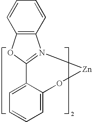
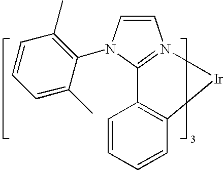
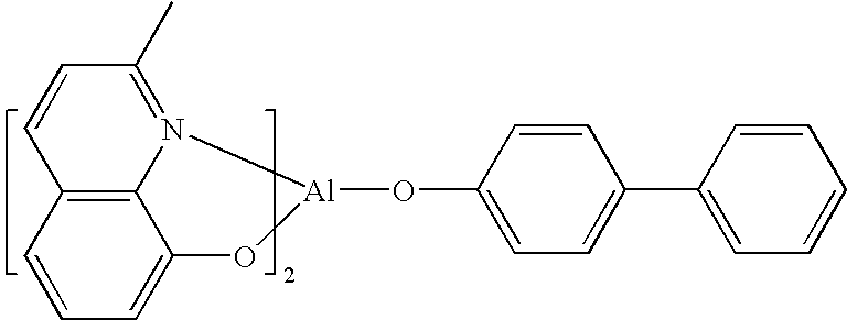
As used herein, the following letter designations refer to compounds as follows:
Figure US08040053-20111018-C00002
Figure US08040053-20111018-C00003

Compounds A and B are an example of a suitable pair of first non-emitting material and first emitting material, respectively. Compounds C and E are an example of a suitable pair of second non-emitting material and second emitting material, respectively. Compounds C and F are another example of a suitable pair of second non-emitting material and second emitting material, respectively. Compounds D and F are another example of a suitable pair of second non-emitting material and second emitting material, respectively. Compound G is used as an emitting material in the examples, and Compound H is used as a hole injection material in the examples. mCBP refers to 3,3′-bis(N-carbazolyl)biphenyl, and NPD refers to 4,4′-bis[N-(1-naphthyl)-N-phenylamino]biphenyl.
Combination with Other Materials
The materials described herein as useful for a particular layer in an organic light emitting device may be used in combination with a wide variety of other materials present in the device. For example, emissive dopants disclosed herein may be used in conjunction with a wide variety of hosts, transport layers, blocking layers, injection layers, electrodes and other layers that may be present. The materials described or referred to below are non-limiting examples of materials that may be useful in combination with the compounds disclosed herein, and one of skill in the art can readily consult the literature to identify other materials that may be useful in combination.
In addition to and/or in combination with the materials disclosed herein, many hole injection materials, hole transporting materials, host materials, dopant materials, exiton/hole blocking layer materials, electron transporting and electron injecting materials may be used in an OLED. Non-limiting examples of the materials that may be used in an OLED in combination with materials disclosed herein are listed in Table 1 below. Table 1 lists non-limiting classes of materials, non-limiting examples of compounds for each class, and references that disclose the materials.
TABLE 1
MATERIAL EXAMPLES OF MATERIAL PUBLICATIONS
Hole injection materials
Phthalocyanine and porphryin compounds
Figure US08040053-20111018-C00004
Appl. Phys. Lett. 69, 2160 (1996)
Starburst triarylamines
Figure US08040053-20111018-C00005
J. Lumin. 72-74, 985 (1997)
CFx Fluorohydrocarbon polymer
Figure US08040053-20111018-C00006
Appl. Phys. Lett. 78, 673 (2001)
Conducting polymers (e.g., PEDOT:PSS, polyaniline, polypthiophene)
Figure US08040053-20111018-C00007
Synth. Met. 87, 171 (1997)
Arylamines complexed with metal oxides such as molybdenum and tungsten oxides
Figure US08040053-20111018-C00008
SID Symposium Digest, 37, 923 (2006)
Hole transporting materials
Triarylamines (e.g., TPD, α-NPD)
Figure US08040053-20111018-C00009
Appl. Phys. Lett. 51, 913 (1987)
Figure US08040053-20111018-C00010
US5061569
Figure US08040053-20111018-C00011
EP650955
Figure US08040053-20111018-C00012
J. Mater. Chem. 3, 319 (1993)
Figure US08040053-20111018-C00013
Appl. Phys. Lett. 90, 183503 (2007)
Figure US08040053-20111018-C00014
Appl. Phys. Lett. 90, 183503 (2007)
Triaylamine on spirofluorene core
Figure US08040053-20111018-C00015
Synth. Met. 91, 209 (1997)
Arylamine carbazole compounds
Figure US08040053-20111018-C00016
Adv. Mater. 6, 677 (1994)
Indolocarbazoles
Figure US08040053-20111018-C00017
Synth. Met. 111, 421 (2000)
Isoindole compounds
Figure US08040053-20111018-C00018
Chem. Mater. 15, 3148 (2003)
Phosphorescent OLED
host materials
Red hosts
Arylcarbazoles
Figure US08040053-20111018-C00019
Appl. Phys. Lett. 78, 1622 (2001)
Metal 8-hydroxyquinolates (e.g., Alq3, BAlq)
Figure US08040053-20111018-C00020
Nature 395, 151 (1998)
Figure US08040053-20111018-C00021
US20060202194
Figure US08040053-20111018-C00022
WO2005014551
Metal phenoxybenzothiazole compounds
Figure US08040053-20111018-C00023
Appl. Phys. Lett. 90, 123509 (2007)
Conjugated oligomers and polymers (e.g., polyfluorene)
Figure US08040053-20111018-C00024
Org. Electron. 1, 15 (2000)
Green hosts
Arylcarbazoles
Figure US08040053-20111018-C00025
Appl. Phys. Lett. 78, 1622 (2001)
Figure US08040053-20111018-C00026
US2003175553
Figure US08040053-20111018-C00027
WO2001039234
Aryltriphenylene compounds
Figure US08040053-20111018-C00028
US20060280965
Figure US08040053-20111018-C00029
US20060280965
Polymers (e.g., PVK)
Figure US08040053-20111018-C00030
Appl. Phys. Lett. 77, 2280 (2000)
Spirofluorene compounds
Figure US08040053-20111018-C00031
WO2004093207
Metal phenoxybenzooxazole compounds
Figure US08040053-20111018-C00032
WO05089025
Figure US08040053-20111018-C00033
WO06132173
Figure US08040053-20111018-C00034
JP200511610
Spirofluorene-carbazole compounds
Figure US08040053-20111018-C00035
JP2007254297
Figure US08040053-20111018-C00036
JP2007254297
Indolocabazoles
Figure US08040053-20111018-C00037
WO07063796
Figure US08040053-20111018-C00038
WO07063754
5-member ring electron deficient heterocycles (e.g., triazole, oxadiazole)
Figure US08040053-20111018-C00039
J. Appl. Phys. 90, 5048 (2001)
Figure US08040053-20111018-C00040
WO04107822
Metal phenoxypyridine compounds
Figure US08040053-20111018-C00041
WO05030900
Blue hosts
Arylcarbazoles
Figure US08040053-20111018-C00042
Appl. Phys. Lett, 82, 2422 (2003)
Figure US08040053-20111018-C00043
US20070190359
Dibenzothiophene- carbazole compounds
Figure US08040053-20111018-C00044
WO2006114966
Phosphorescent dopants
Red dopants
Heavy metal porphyrins (e.g., PtOEP)
Figure US08040053-20111018-C00045
Nature 395, 151 (1998)
Iridium(III) organometallic complexes
Figure US08040053-20111018-C00046
Appl. Phys. Lett. 78, 1622 (2001)
Figure US08040053-20111018-C00047
US06835469
Figure US08040053-20111018-C00048
US06835469
Figure US08040053-20111018-C00049
US20060202194
Figure US08040053-20111018-C00050
US20060202194
Figure US08040053-20111018-C00051
US07087321
Figure US08040053-20111018-C00052
US07087321
Figure US08040053-20111018-C00053
Adv. Mater. 19, 739 (2007)
Platinum(II) organometallic complexes
Figure US08040053-20111018-C00054
WO2003040257
Osminum(III) complexes
Figure US08040053-20111018-C00055
Chem. Mater. 17, 3532 (2005)
Ruthenium(II) complexes
Figure US08040053-20111018-C00056
Adv. Mater. 17, 1059 (2005)
Green dopants
Iridium(III) organometallic complexes
Figure US08040053-20111018-C00057
Inorg. Chem. 40, 1704 (2001)
Figure US08040053-20111018-C00058
US2002034656
Figure US08040053-20111018-C00059
US06687266
Figure US08040053-20111018-C00060
Chem. Mater. 16, 2480 (2004)
Figure US08040053-20111018-C00061
US2007190359
Figure US08040053-20111018-C00062
US 2006008670 JP2007123392
Figure US08040053-20111018-C00063
Adv. Mater. 16, 2003 (2004)
Figure US08040053-20111018-C00064
Angew. Chem. Int. Ed. 2006, 45, 7800
Pt(II) organometallic complexes
Figure US08040053-20111018-C00065
Appl. Phys. Lett. 86, 153505 (2005)
Figure US08040053-20111018-C00066
Appl. Phys. Lett. 86, 153505 (2005)
Figure US08040053-20111018-C00067
Chem. Lett. 34, 592 (2005)
Gold complexes
Figure US08040053-20111018-C00068
Chem. Commun. 2906 (2005)
Rhenium(III) complexes
Figure US08040053-20111018-C00069
Inorg. Chem. 42, 1248 (2003)
Blue dopants
Iridium(III) organometallic complexes
Figure US08040053-20111018-C00070
WO2002002714
Figure US08040053-20111018-C00071
WO2006009024
Figure US08040053-20111018-C00072
US2006251923
Figure US08040053-20111018-C00073
WO2006056418, US2005260441
Figure US08040053-20111018-C00074
US2007190359
Figure US08040053-20111018-C00075
US2002134984
Figure US08040053-20111018-C00076
Angew. Chem. Int. Ed. 47, 1 (2008)
Figure US08040053-20111018-C00077
Chem. Mater. 18, 5119 (2006)
Figure US08040053-20111018-C00078
Inorg. Chem. 46, 4308 (2007)
Figure US08040053-20111018-C00079
WO05123873
Figure US08040053-20111018-C00080
WO05123873
Figure US08040053-20111018-C00081
WO07004380
Figure US08040053-20111018-C00082
WO06082742
Osmium(II) complexes
Figure US08040053-20111018-C00083
US2005260449
Figure US08040053-20111018-C00084
Organometallics 23, 3745 (2004)
Gold complexes
Figure US08040053-20111018-C00085
Appl. Phys. Lett. 74, 1361 (1999)
Platinum(II) complexes
Figure US08040053-20111018-C00086
WO06098120, WO06103874
Exciton/hole blocking
layer materials
Bathocuprine compounds (e.g., BCP, BPhen)
Figure US08040053-20111018-C00087
Appl. Phys. Lett. 75, 4 (1999)
Figure US08040053-20111018-C00088
Appl. Phys. Lett. 79, 449 (2001)
Metal 8-hydroxyquinolates (e.g., BAlq)
Figure US08040053-20111018-C00089
Appl. Phys. Lett. 81, 162 (2002)
5-member ring electron deficient heterocycles such as triazole, oxadiazole, imidazole, benzoimidazole
Figure US08040053-20111018-C00090
Appl. Phys. Lett. 81, 162 (2002)
Triphenylene compounds
Figure US08040053-20111018-C00091
US20050025993
Fluorinated aromatic compounds
Figure US08040053-20111018-C00092
Appl. Phys. Lett. 79, 156 (2001)
Electron transporting
materials
Anthracene- benzoimidazole compounds
Figure US08040053-20111018-C00093
WO03060956
Anthracene-benzothiazole compounds
Figure US08040053-20111018-C00094
Appl. Phys. Lett. 89, 063504 (2006)
Metal 8-hydroxyquinolates (e.g., Alq3)
Figure US08040053-20111018-C00095
Appl. Phys. Lett. 51, 913 (1987)
Metal hydroxybenoquinolates
Figure US08040053-20111018-C00096
Chem. Lett. 5, 905 (1993)
Bathocuprine compounds such as BCP, BPhen, etc
Figure US08040053-20111018-C00097
Appl. Phys. Lett. 91, 263503 (2007)
Figure US08040053-20111018-C00098
Appl. Phys. Lett. 79, 449 (2001)
5-member ring electron deficient heterocycles (e.g., triazole, oxadiazole, imidazole, benzoimidazole)
Figure US08040053-20111018-C00099
Appl. Phys. Lett. 74, 865 (1999)
Figure US08040053-20111018-C00100
Appl. Phys. Lett. 55, 1489 (1989)
Figure US08040053-20111018-C00101
Jpn. J. Apply. Phys. 32, L917 (1993)
Silole compounds
Figure US08040053-20111018-C00102
Org. Electron. 4, 113 (2003)
Arylborane compounds
Figure US08040053-20111018-C00103
J. Am. Chem. Soc. 120, 9714 (1998)
Fluorinated aromatic compounds
Figure US08040053-20111018-C00104
J. Am. Chem. Soc. 122, 1832 (2000)
EXAMPLES
A number of devices were fabricated by thermal evaporation of the various layers layers, in sequence, on a commercially available ITO coated substrate. Table 2 shows the structure of various devices fabricated. Where a thickness appears at the head of a column, the layer corresponding to that column had that thickness in all devices. All concentrations are wt %, and where a concentration for a particular material is not specified, the material makes up the remainder of the material in the layer for which a concentration is not already specified, i.e., Device 1 has ITO/A (100 wt %)/A (99.5 wt %):B (0.5 wt %)/and so on.
TABLE 2
Device structures
Device No. [10 nm] [20 nm] [15 nm] [40 nm] [90 nm]
1 ITO A A:B 0.5% C:E D LG201 LiF/Al
 [80 nm] 18% [5 nm]
2 ITO A A:B 1% C:E D LG201 LiF/Al
 [80 nm] 18% [5 nm]
3 ITO A A:B 1% C:E D LG201 LiF/Al
 [80 nm] 18% [5 nm]
4 ITO A A:B 0.5% C:E D LG201 LiF/Al
[120 nm] 15% [5 nm]
5 ITO A A:B 0.5% C:E C LG201 LiF/Al
[120 nm] 15% [5 nm]
6 ITO A A:B 0.5% C:E LG201 LiF/Al
[120 nm] 15%
7 ITO A A:B 0.5% C:F D LG201 LiF/Al
[120 nm] 18% [5 nm]
8 ITO A A:B 0.5% C:F C LG201 LiF/Al
[120 nm] 18% [5 nm]
9 ITO A A:B 0.5% C:F LG201 LiF/Al
[120 nm] 18%
10 ITO A A:B 0.5% D:F D LG201 LiF/Al
[120 nm] 18% [5 nm]
11 ITO A A:B 0.5% D:F C LG201 LiF/Al
[120 nm] 18% [5 nm]
12 ITO A A:B 0.5% D:F LG201 LiF/Al
[120 nm] 18%
13 ITO A A:B 0.5% C:E D LG201 LiF/Al
 [80 nm] 15% [5 nm]
14 ITO A A:B 0.5% C:E C LG201 LiF/Al
 [80 nm] 15% [5 nm]
15 ITO A A:B 0.5% C:E LG201 LiF/Al
 [80 nm] 15%
16 ITO A A:B 0.5% C:F D LG201 LiF/Al
 [80 nm] 18% [5 nm]
17 ITO A A:B 0.5% C:F C LG201 LiF/Al
 [80 nm] 18% [5 nm]
18 ITO A A:B 0.5% C:F LG201 LiF/Al
 [80 nm] 18%
19 ITO A A:B 0.5% D:F D LG201 LiF/Al
 [80 nm] 18% [5 nm]
20 ITO A A:B 0.5% D:F C LG201 LiF/Al
 [80 nm] 18% [5 nm]
21 ITO A A:B 0.5% D:F LG201 LiF/Al
 [80 nm] 18%
22 ITO A A:B 0.5% C:E C LG201 LiF/Al
[120 nm] 15% [5 nm]
23 ITO A A:B 0.5% C:E:A C LG201 LiF/Al
[120 nm] 15%:0.5% [5 nm]
24 ITO A A:B 0.5% C:E:A C LG201 LiF/Al
[120 nm] 15%:0.5% [5 nm]
Devices 25 and 26, which are not included in the table due to different layer thicknesses, had the following structures:
  • Device 25: ITO(120 nm)/A(10 nm)/A:B[0.5%](20 nm)/mCBP:G [15%](15 nm)/mCBP(5 nm)/LG201(30 mm)/LiF/Al
  • Device 26: ITO(120 nm)/H(30 nm)/NPD(10 nm)/A:B[0.5%](20 nm)/mCBP:G[15%](15 nm)/mCBP 5 nm)/LG201(30 nm)/LiF/Al
Table 3 shows measured device performance characteristics for the devices described in Table 2. Voltage, luminous efficacy (in candelas per amp), external quantum efficiency, and power efficiency were measured at a luminance of 1000 nits. 1931 CIE coordinates were measured at a current density of 10 mA/cm2.
TABLE 3
Device Performance Characteristics
At 1000 nits. At 10 mA/cm2
Luminous Power 1931
Voltage Efficacy EQE Efficiency 1931 CIE CIE
Device No. [V] cd/A [%] [Lm/W] x y
1 4.5 33.1 16.7 22.9 0.442 0.443
2 4.5 33.8 17.8 23.6 0.456 0.434
3 4.5 25.7 13.2 17.9 0.437 0.445
4 4.3 34.3 16.1 25.3 0.416 0.429
5 5.0 17.4 8.1 10.8 0.407 0.429
6 5.1 6.4 3.0 4.0 0.402 0.427
7 4.3 43.3 18.8 31.4 0.424 0.475
8 4.7 31.8 13.7 21.3 0.415 0.476
9 4.5 15.4 6.4 10.6 0.388 0.487
10 4.8 28.7 13.7 18.9 0.473 0.450
11 5.1 21.2 10.2 13.1 0.480 0.447
12 4.5 20.5 9.5 14.4 0.455 0.456
13 4.3 32.4 17.0 23.7 0.395 0.395
14 5.1 17.4 9.0 10.8 0.379 0.393
15 5.2 7.0 3.6 4.2 0.378 0.391
16 4.6 36.0 17.3 24.5 0.414 0.454
17 5.1 29.9 14.1 18.4 0.396 0.455
18 4.8 18.3 8.6 12.0 0.393 0.456
19 5.2 21.0 10.7 12.6 0.444 0.438
20 5.6 18.4 9.4 10.3 0.450 0.437
21 4.9 16.8 8.5 10.8 0.442 0.439
22 4.6 10.7 5.1 7.3 0.422 0.423
23 4.6 11.7 5.0 7.9 0.423 0.463
24 4.5 14.3 5.5 9.9 0.402 0.493
25 4.9 16.7 9.3 10.6 0.280 0.310
26 5.3 14.9 8.3 8.7 0.323 0.322
The measured device results show that devices having a combination of first emissive and non-emissive layers sharing a common first non-emissive material, and second emissive and non-emissive layer sharing a common second non-emissive material, show results unexepectedly superior to devices lacking the second non-emissive layer. All devices in Tables 2 and 3, with the exception of Device 26 which is a comparative example, have a first emissive layer that is 20 nm non-emitting Compound A doped with 0.5 wt % emitting Compound B, and a first non-emissive layer that is 10 nm of Compound A, where Compound A is the first non-emitting material that is common to the two layers. Some of the devices, specifically Device Nos. 5, 10, 14, 17, 19, 22, 23, and 24 also have a second emissive layer that is 15 nm of either non-emitting Compound C or D doped with emitting Compounds E, F and/or A, and a second non-emissive layer that is 5 nm of Compound C or D, where Compound C or D is the second non-emitting material that is common to the two layers. Other devices in the table use a non-emitting material in the second non-emissive layer that is different from the non-emitting material in the second emitting layer, or lack the second non-emissive layer.
By comparing Device Nos. 5, 10, 14, 17 and 19 to Device Nos. 6, 12, 15, 18 and 21, respectively, it can be seen that the addition of a second non-emissive layer made of the same non-emitting material that is present in the second emissive layer dramatically improves device external quantum efficiency and power efficiency.
It should also be noted that Compound D appears to be a better electron transport material than Compound C across various devices in Tables 2 and 3. The specific comparisons noted in the prior paragraph control for and remove effects caused by one specific material being better than another specific material, and isolate the effect caused by using a second non-emissive layer comprising the same non-emitting material as the second emissive layer.
Comparing Device No. 25 and 26 shows that the use of a first non-emissive layer comprising a first non-emitting material, which is also used in an adjacent emissive layer comprising the first non-emitting material and a first emitting material, as in Device No. 25, may provide superior efficiency as compared to an otherwise identical device that uses a common hole-injection/hole transport material selection (Device No. 26).
It is understood that the various embodiments described herein are by way of example only, and are not intended to limit the scope of the invention. For example, many of the materials and structures described herein may be substituted with other materials and structures without deviating from the spirit of the invention. The present invention as claimed may therefore includes variations from the particular examples and preferred embodiments described herein, as will be apparent to one of skill in the art. It is understood that various theories as to why the invention works are not intended to be limiting.

Claims (12)

1. An organic light emitting device, comprising:
an anode;
a cathode;
a first emissive layer disposed between the anode and the cathode, the first emissive layer comprising:
a first non-emitting organic material, wherein the first non-emitting material is organometallic and is present in the first emissive layer in a concentration of at least 50 wt %; and
a first emitting organic material;
a second emissive layer disposed between the first emissive layer and the cathode, and in direct contact with the first emissive layer, the second emissive layer comprising:
a second non-emitting organic material; and
a second emitting organic material;
a first non-emissive layer disposed between the first emissive layer and the anode, and in direct contact with the first emissive layer, the first non-emissive layer comprising the first non-emissive organic material.
2. The device of claim 1, further comprising a second non-emissive layer disposed between the second emissive layer and the cathode, and in direct contact with the second emissive layer, the second non-emissive layer comprising the second non-emitting organic material.
3. The device of claim 2, wherein the first and second emitting organic materials are phosphorescent materials.
4. The device of claim 2, wherein the first emitting organic material is present in the first emissive layer in a concentration of 0.1 to 6 wt %.
5. The device of claim 4, wherein the first emitting organic material is present in the first emissive layer in a concentration of 0.1 to 3 wt %.
6. The device of claim 2, wherein:
the first emissive layer consists essentially of the first non-emitting organic material and the first emitting organic material;
the first non-emissive layer consists essentially of the first non-emitting organic material;
the second emissive layer consists essentially of the second non-emitting organic material and the second emitting organic material;
the second non-emissive layer consists essentially of the second non-emitting organic material.
7. The device of claim 6, further comprising a third non-emissive layer disposed between the second non-emissive layer and the cathode, and in direct contact with the second non-emissive layer and the cathode, the third non-emissive layer comprising a third non-emitting material.
8. The device of claim 7, wherein the third non-emissive layer consists essentially of a third non-emitting material.
9. The device of claim 8, wherein the first non-emissive layer is in direct contact with the anode.
10. The device of claim 9, wherein the device consists essentially of the anode, the cathode, the first and second emitting materials, and the first, second and third non-emitting materials.
11. The device of claim 2, wherein the second emissive layer further comprises a fourth non-emitting material.
12. The device of claim 2, wherein the first emitting material has a peak emissive wavelength in the visible spectrum of 500-700 nm, and the second emitting material has a peak emissive wavelength in the visible spectrum of 400-500 nm.
US12/332,945 2008-02-09 2008-12-11 Organic light emitting device architecture for reducing the number of organic materials Active 2029-07-07 US8040053B2 (en)

Priority Applications (3)

Application Number Priority Date Filing Date Title
US12/332,945 US8040053B2 (en) 2008-02-09 2008-12-11 Organic light emitting device architecture for reducing the number of organic materials
PCT/US2009/030545 WO2009099705A1 (en) 2008-02-09 2009-01-09 Organic licht emitting device with a non-emissive organometallic layer
TW098102101A TWI527498B (en) 2008-02-09 2009-01-20 Organic light emitting device architecture

Applications Claiming Priority (2)

Application Number Priority Date Filing Date Title
US6513108P 2008-02-09 2008-02-09
US12/332,945 US8040053B2 (en) 2008-02-09 2008-12-11 Organic light emitting device architecture for reducing the number of organic materials

Publications (2)

Publication Number Publication Date
US20090200927A1 US20090200927A1 (en) 2009-08-13
US8040053B2 true US8040053B2 (en) 2011-10-18

Family

ID=40938329

Family Applications (1)

Application Number Title Priority Date Filing Date
US12/332,945 Active 2029-07-07 US8040053B2 (en) 2008-02-09 2008-12-11 Organic light emitting device architecture for reducing the number of organic materials

Country Status (3)

Country Link
US (1) US8040053B2 (en)
TW (1) TWI527498B (en)
WO (1) WO2009099705A1 (en)

Cited By (3)

* Cited by examiner, † Cited by third party
Publication number Priority date Publication date Assignee Title
US10355246B2 (en) 2015-12-16 2019-07-16 Oti Lumionics Inc. Barrier coating for opto-electronics devices
US10439081B2 (en) 2012-11-06 2019-10-08 Oti Lumionics Inc. Method for depositing a conductive coating on a surface
US11152587B2 (en) 2016-08-15 2021-10-19 Oti Lumionics Inc. Light transmissive electrode for light emitting devices

Families Citing this family (13)

* Cited by examiner, † Cited by third party
Publication number Priority date Publication date Assignee Title
US8586204B2 (en) * 2007-12-28 2013-11-19 Universal Display Corporation Phosphorescent emitters and host materials with improved stability
JP5515283B2 (en) * 2008-12-10 2014-06-11 コニカミノルタ株式会社 Organic electroluminescence element, display device and lighting device
KR20120103571A (en) * 2009-10-05 2012-09-19 손 라이팅 리미티드 Multilayer organic device
JP5934656B2 (en) 2010-02-05 2016-06-15 日東電工株式会社 Organic light emitting diode with improved efficiency
US9156870B2 (en) * 2010-02-25 2015-10-13 Universal Display Corporation Phosphorescent emitters
TW201210403A (en) * 2010-08-25 2012-03-01 Nat Univ Tsing Hua Organic light emitting diode
JP5815341B2 (en) 2010-09-09 2015-11-17 株式会社半導体エネルギー研究所 Heterocyclic compounds
CN103229323B (en) 2010-11-11 2016-08-31 日东电工株式会社 Mix composite emitting structural and use the light-emitting device of this emitting structural
JP6675193B2 (en) * 2011-03-31 2020-04-01 ユー・ディー・シー アイルランド リミテッド Host material of organic electroluminescent device, organic electroluminescent device, light emitting device, display device, and lighting device
WO2013058087A1 (en) * 2011-10-21 2013-04-25 コニカミノルタ株式会社 Organic electroluminscent element
JP6197650B2 (en) * 2011-12-20 2017-09-20 コニカミノルタ株式会社 Organic EL device
CN104245715A (en) * 2012-04-23 2014-12-24 E.I.内穆尔杜邦公司 Blue luminescent compounds
KR102273616B1 (en) * 2014-12-08 2021-07-06 엘지디스플레이 주식회사 Organic light emitting device

Citations (77)

* Cited by examiner, † Cited by third party
Publication number Priority date Publication date Assignee Title
US4769292A (en) 1987-03-02 1988-09-06 Eastman Kodak Company Electroluminescent device with modified thin film luminescent zone
US5061569A (en) 1990-07-26 1991-10-29 Eastman Kodak Company Electroluminescent device with organic electroluminescent medium
US5247190A (en) 1989-04-20 1993-09-21 Cambridge Research And Innovation Limited Electroluminescent devices
EP0650955A1 (en) 1993-11-01 1995-05-03 Hodogaya Chemical Co., Ltd. Amine compound and electro-luminescence device comprising same
US5703436A (en) 1994-12-13 1997-12-30 The Trustees Of Princeton University Transparent contacts for organic devices
US5707745A (en) 1994-12-13 1998-01-13 The Trustees Of Princeton University Multicolor organic light emitting devices
US5834893A (en) 1996-12-23 1998-11-10 The Trustees Of Princeton University High efficiency organic light emitting devices with light directing structures
US5844363A (en) 1997-01-23 1998-12-01 The Trustees Of Princeton Univ. Vacuum deposited, non-polymeric flexible organic light emitting devices
US6013982A (en) 1996-12-23 2000-01-11 The Trustees Of Princeton University Multicolor display devices
US6087196A (en) 1998-01-30 2000-07-11 The Trustees Of Princeton University Fabrication of organic semiconductor devices using ink jet printing
US6091195A (en) 1997-02-03 2000-07-18 The Trustees Of Princeton University Displays having mesa pixel configuration
US6097147A (en) 1998-09-14 2000-08-01 The Trustees Of Princeton University Structure for high efficiency electroluminescent device
WO2001039234A2 (en) 1999-11-24 2001-05-31 The Trustees Of Princeton University Organic light emitting diode having a blue phosphorescent molecule as an emitter
US6294398B1 (en) 1999-11-23 2001-09-25 The Trustees Of Princeton University Method for patterning devices
US6303238B1 (en) 1997-12-01 2001-10-16 The Trustees Of Princeton University OLEDs doped with phosphorescent compounds
US6337102B1 (en) 1997-11-17 2002-01-08 The Trustees Of Princeton University Low pressure vapor phase deposition of organic thin films
WO2002002714A2 (en) 2000-06-30 2002-01-10 E.I. Du Pont De Nemours And Company Electroluminescent iridium compounds with fluorinated phenylpyridines, phenylpyrimidines, and phenylquinolines and devices made with such compounds
US20020034656A1 (en) 1998-09-14 2002-03-21 Thompson Mark E. Organometallic complexes as phosphorescent emitters in organic LEDs
US20020134984A1 (en) 2001-02-01 2002-09-26 Fuji Photo Film Co., Ltd. Transition metal complex and light-emitting device
WO2003040257A1 (en) 2001-11-07 2003-05-15 E. I. Du Pont De Nemours And Company Electroluminescent platinum compounds and devices made with such compounds
WO2003060956A2 (en) 2002-01-18 2003-07-24 Lg Chem, Ltd. New material for transporting electrons and organic electroluminescent display using the same
JP2003229272A (en) 2002-01-31 2003-08-15 Toyota Industries Corp Organic el element
US20030175553A1 (en) 2001-12-28 2003-09-18 Thompson Mark E. White light emitting oleds from combined monomer and aggregate emission
US20030230980A1 (en) 2002-06-18 2003-12-18 Forrest Stephen R Very low voltage, high efficiency phosphorescent oled in a p-i-n structure
US6687266B1 (en) 2002-11-08 2004-02-03 Universal Display Corporation Organic light emitting materials and devices
US20040174116A1 (en) 2001-08-20 2004-09-09 Lu Min-Hao Michael Transparent electrodes
WO2004093207A2 (en) 2003-04-15 2004-10-28 Covion Organic Semiconductors Gmbh Mixtures of matrix materials and organic semiconductors capable of emission, use of the same and electronic components containing said mixtures
WO2004107822A1 (en) 2003-05-29 2004-12-09 Nippon Steel Chemical Co., Ltd. Organic electroluminescent element
US6835469B2 (en) 2001-10-17 2004-12-28 The University Of Southern California Phosphorescent compounds and devices comprising the same
JP2005011610A (en) 2003-06-18 2005-01-13 Nippon Steel Chem Co Ltd Organic electroluminescent element
US20050025993A1 (en) 2003-07-25 2005-02-03 Thompson Mark E. Materials and structures for enhancing the performance of organic light emitting devices
JP2005038672A (en) 2003-07-18 2005-02-10 Konica Minolta Holdings Inc Organic electroluminescent element, lighting device, and display device
WO2005014551A1 (en) 2003-08-07 2005-02-17 Nippon Steel Chemical Co., Ltd. Aluminum chelate compelx for organic el material
US20050046337A1 (en) * 2003-09-03 2005-03-03 Byung-Doo Chin Organic lights-emitting device with doped emission layer
US6869695B2 (en) 2001-12-28 2005-03-22 The Trustees Of Princeton University White light emitting OLEDs from combined monomer and aggregate emission
US20050074630A1 (en) 2003-03-27 2005-04-07 Hiroshi Kanno Organic electroluminescent device
WO2005030900A1 (en) 2003-09-25 2005-04-07 Nippon Steel Chemical Co., Ltd. Organic electroluminescent device
US20050077817A1 (en) * 2002-12-26 2005-04-14 Semiconductor Energy Laboratory Co., Ltd. Organic light emitting element and a light emitting device using the same
WO2005089025A1 (en) 2004-03-15 2005-09-22 Nippon Steel Chemical Co., Ltd. Organic electroluminescent device
EP1589789A1 (en) 2003-01-24 2005-10-26 Idemitsu Kosan Co., Ltd. Organic electroluminescence device
US20050260449A1 (en) 2004-05-18 2005-11-24 Robert Walters Complexes with tridentate ligands
US20050260441A1 (en) 2004-05-18 2005-11-24 Thompson Mark E Luminescent compounds with carbene ligands
WO2005123873A1 (en) 2004-06-17 2005-12-29 Konica Minolta Holdings, Inc. Organic electroluminescent device material, organic electroluminescent device, display and illuminating device
US20060008670A1 (en) 2004-07-06 2006-01-12 Chun Lin Organic light emitting materials and devices
WO2006009024A1 (en) 2004-07-23 2006-01-26 Konica Minolta Holdings, Inc. Organic electroluminescent device, display and illuminating device
US20060046098A1 (en) 2000-03-27 2006-03-02 Idemitsu Kosan Co., Ltd. Organic electroluminescence element
US7009338B2 (en) 2001-05-16 2006-03-07 The University Of Southern California High efficiency multi-color electro-phosphorescent OLEDs
US7022421B2 (en) 2001-08-29 2006-04-04 The University Of Southern California Organic light emitting devices having carrier blocking layers comprising metal complexes
WO2006056418A2 (en) 2004-11-25 2006-06-01 Basf Aktiengesellschaft Use of transition metal carbene complexes in organic light-emitting diodes (oleds)
EP1670082A2 (en) 2004-12-13 2006-06-14 Kabushiki Kaisha Toyota Jidoshokki Organic el devices
US20060141288A1 (en) 2001-05-24 2006-06-29 Idemitsu Kosan Co., Ltd. Organic electroluminescence element
US7078113B2 (en) 2001-08-29 2006-07-18 The University Of Southern California Organic light emitting devices having carrier transporting layers comprising metal complexes
US7087321B2 (en) 2003-04-22 2006-08-08 Universal Display Corporation Organic light emitting devices having reduced pixel shrinkage
WO2006082742A1 (en) 2005-02-04 2006-08-10 Konica Minolta Holdings, Inc. Organic electroluminescent device material, organic electroluminescent device, display and illuminating device
US20060202194A1 (en) 2005-03-08 2006-09-14 Jeong Hyun C Red phosphorescene compounds and organic electroluminescence device using the same
WO2006098120A1 (en) 2005-03-16 2006-09-21 Konica Minolta Holdings, Inc. Organic electroluminescent device material and organic electroluminescent device
WO2006103874A1 (en) 2005-03-29 2006-10-05 Konica Minolta Holdings, Inc. Organic electroluminescent device material, organic electroluminescent device, display and illuminating device
US20060232194A1 (en) 2005-04-13 2006-10-19 Yeh-Jiun Tung Hybrid OLED having phosphorescent and fluorescent emitters
WO2006114966A1 (en) 2005-04-18 2006-11-02 Konica Minolta Holdings, Inc. Organic electroluminescent device, display and illuminating device
US20060251923A1 (en) 2005-05-06 2006-11-09 Chun Lin Stability OLED materials and devices
WO2006132173A1 (en) 2005-06-07 2006-12-14 Nippon Steel Chemical Co., Ltd. Organic metal complex and organic electroluminescent device using same
US7151339B2 (en) 2004-01-30 2006-12-19 Universal Display Corporation OLED efficiency by utilization of different doping concentrations within the device emissive layer
WO2007004380A1 (en) 2005-07-01 2007-01-11 Konica Minolta Holdings, Inc. Organic electroluminescent element material, organic electroluminescent element, display device, and lighting equipment
JP2007123392A (en) 2005-10-26 2007-05-17 Konica Minolta Holdings Inc Organic electroluminescence device, display device and lighting device
WO2007063754A1 (en) 2005-12-01 2007-06-07 Nippon Steel Chemical Co., Ltd. Compound for organic electroluminescent element and organic electroluminescent element
WO2007063796A1 (en) 2005-12-01 2007-06-07 Nippon Steel Chemical Co., Ltd. Organic electroluminescent device
US20070190359A1 (en) 2006-02-10 2007-08-16 Knowles David B Metal complexes of cyclometallated imidazo[1,2-ƒ]phenanthridine and diimidazo[1,2-a:1',2'-c]quinazoline ligands and isoelectronic and benzannulated analogs thereof
JP2007254297A (en) 2006-03-20 2007-10-04 Nippon Steel Chem Co Ltd Compound of light-emitting layer and organic electroluminescent device
US7294849B2 (en) 2001-03-14 2007-11-13 The Trustees Of Princeton University Materials and devices for blue phosphorescence based organic light emitting diodes
US7431968B1 (en) 2001-09-04 2008-10-07 The Trustees Of Princeton University Process and apparatus for organic vapor jet deposition
US7466073B2 (en) * 2004-09-29 2008-12-16 Canon Kabushiki Kaisha Organic electroluminescent device and display apparatus
WO2009030981A2 (en) 2006-12-28 2009-03-12 Universal Display Corporation Long lifetime phosphorescent organic light emitting device (oled) structures
WO2010028262A1 (en) 2008-09-04 2010-03-11 Universal Display Corporation White phosphorescent organic light emitting devices
US7714498B2 (en) * 2004-06-07 2010-05-11 Panasonic Corporation Electroluminescent device with acetylacetonato complex salt included in phosphor layer
US7768195B2 (en) * 2006-05-25 2010-08-03 Idemitsu Kosan Co., Ltd. Organic electroluminescent device with improved luminous efficiency
US7862906B2 (en) * 2003-04-09 2011-01-04 Semiconductor Energy Laboratory Co., Ltd. Electroluminescent element and light-emitting device
US7871711B2 (en) * 2004-03-31 2011-01-18 Fujifilm Corporation Organic electroluminescent element and organic electroluminescent display

Family Cites Families (2)

* Cited by examiner, † Cited by third party
Publication number Priority date Publication date Assignee Title
US700938A (en) * 1902-03-01 1902-05-27 Robert W Johnson Bandage.
US7755278B2 (en) * 2004-08-25 2010-07-13 Semiconductor Energy Laboratory Co., Ltd. Light emitting element provided with organic conductive and inorganic hole transport layers between an electrode and organic emissive layer

Patent Citations (82)

* Cited by examiner, † Cited by third party
Publication number Priority date Publication date Assignee Title
US4769292A (en) 1987-03-02 1988-09-06 Eastman Kodak Company Electroluminescent device with modified thin film luminescent zone
US5247190A (en) 1989-04-20 1993-09-21 Cambridge Research And Innovation Limited Electroluminescent devices
US5061569A (en) 1990-07-26 1991-10-29 Eastman Kodak Company Electroluminescent device with organic electroluminescent medium
EP0650955A1 (en) 1993-11-01 1995-05-03 Hodogaya Chemical Co., Ltd. Amine compound and electro-luminescence device comprising same
US5703436A (en) 1994-12-13 1997-12-30 The Trustees Of Princeton University Transparent contacts for organic devices
US5707745A (en) 1994-12-13 1998-01-13 The Trustees Of Princeton University Multicolor organic light emitting devices
US5834893A (en) 1996-12-23 1998-11-10 The Trustees Of Princeton University High efficiency organic light emitting devices with light directing structures
US6013982A (en) 1996-12-23 2000-01-11 The Trustees Of Princeton University Multicolor display devices
US5844363A (en) 1997-01-23 1998-12-01 The Trustees Of Princeton Univ. Vacuum deposited, non-polymeric flexible organic light emitting devices
US6091195A (en) 1997-02-03 2000-07-18 The Trustees Of Princeton University Displays having mesa pixel configuration
US6337102B1 (en) 1997-11-17 2002-01-08 The Trustees Of Princeton University Low pressure vapor phase deposition of organic thin films
US6303238B1 (en) 1997-12-01 2001-10-16 The Trustees Of Princeton University OLEDs doped with phosphorescent compounds
US6087196A (en) 1998-01-30 2000-07-11 The Trustees Of Princeton University Fabrication of organic semiconductor devices using ink jet printing
US6097147A (en) 1998-09-14 2000-08-01 The Trustees Of Princeton University Structure for high efficiency electroluminescent device
US20020034656A1 (en) 1998-09-14 2002-03-21 Thompson Mark E. Organometallic complexes as phosphorescent emitters in organic LEDs
US6294398B1 (en) 1999-11-23 2001-09-25 The Trustees Of Princeton University Method for patterning devices
US6468819B1 (en) 1999-11-23 2002-10-22 The Trustees Of Princeton University Method for patterning organic thin film devices using a die
WO2001039234A2 (en) 1999-11-24 2001-05-31 The Trustees Of Princeton University Organic light emitting diode having a blue phosphorescent molecule as an emitter
US20060046098A1 (en) 2000-03-27 2006-03-02 Idemitsu Kosan Co., Ltd. Organic electroluminescence element
WO2002002714A2 (en) 2000-06-30 2002-01-10 E.I. Du Pont De Nemours And Company Electroluminescent iridium compounds with fluorinated phenylpyridines, phenylpyrimidines, and phenylquinolines and devices made with such compounds
US20020134984A1 (en) 2001-02-01 2002-09-26 Fuji Photo Film Co., Ltd. Transition metal complex and light-emitting device
US7294849B2 (en) 2001-03-14 2007-11-13 The Trustees Of Princeton University Materials and devices for blue phosphorescence based organic light emitting diodes
US7285907B2 (en) * 2001-05-16 2007-10-23 The University Of Southern California High efficiency multi-color electro-phosphorescent OLEDs
US7009338B2 (en) 2001-05-16 2006-03-07 The University Of Southern California High efficiency multi-color electro-phosphorescent OLEDs
US20060141288A1 (en) 2001-05-24 2006-06-29 Idemitsu Kosan Co., Ltd. Organic electroluminescence element
US20040174116A1 (en) 2001-08-20 2004-09-09 Lu Min-Hao Michael Transparent electrodes
US7078113B2 (en) 2001-08-29 2006-07-18 The University Of Southern California Organic light emitting devices having carrier transporting layers comprising metal complexes
US7022421B2 (en) 2001-08-29 2006-04-04 The University Of Southern California Organic light emitting devices having carrier blocking layers comprising metal complexes
US7431968B1 (en) 2001-09-04 2008-10-07 The Trustees Of Princeton University Process and apparatus for organic vapor jet deposition
US6835469B2 (en) 2001-10-17 2004-12-28 The University Of Southern California Phosphorescent compounds and devices comprising the same
WO2003040257A1 (en) 2001-11-07 2003-05-15 E. I. Du Pont De Nemours And Company Electroluminescent platinum compounds and devices made with such compounds
US20030175553A1 (en) 2001-12-28 2003-09-18 Thompson Mark E. White light emitting oleds from combined monomer and aggregate emission
US6869695B2 (en) 2001-12-28 2005-03-22 The Trustees Of Princeton University White light emitting OLEDs from combined monomer and aggregate emission
WO2003060956A2 (en) 2002-01-18 2003-07-24 Lg Chem, Ltd. New material for transporting electrons and organic electroluminescent display using the same
JP2003229272A (en) 2002-01-31 2003-08-15 Toyota Industries Corp Organic el element
US20030230980A1 (en) 2002-06-18 2003-12-18 Forrest Stephen R Very low voltage, high efficiency phosphorescent oled in a p-i-n structure
US6687266B1 (en) 2002-11-08 2004-02-03 Universal Display Corporation Organic light emitting materials and devices
US20050077817A1 (en) * 2002-12-26 2005-04-14 Semiconductor Energy Laboratory Co., Ltd. Organic light emitting element and a light emitting device using the same
EP1589789A1 (en) 2003-01-24 2005-10-26 Idemitsu Kosan Co., Ltd. Organic electroluminescence device
US20050074630A1 (en) 2003-03-27 2005-04-07 Hiroshi Kanno Organic electroluminescent device
US7611779B2 (en) * 2003-03-27 2009-11-03 Sanyo Electric Co., Ltd. Organic electroluminescent device
US7862906B2 (en) * 2003-04-09 2011-01-04 Semiconductor Energy Laboratory Co., Ltd. Electroluminescent element and light-emitting device
WO2004093207A2 (en) 2003-04-15 2004-10-28 Covion Organic Semiconductors Gmbh Mixtures of matrix materials and organic semiconductors capable of emission, use of the same and electronic components containing said mixtures
US7087321B2 (en) 2003-04-22 2006-08-08 Universal Display Corporation Organic light emitting devices having reduced pixel shrinkage
WO2004107822A1 (en) 2003-05-29 2004-12-09 Nippon Steel Chemical Co., Ltd. Organic electroluminescent element
JP2005011610A (en) 2003-06-18 2005-01-13 Nippon Steel Chem Co Ltd Organic electroluminescent element
JP2005038672A (en) 2003-07-18 2005-02-10 Konica Minolta Holdings Inc Organic electroluminescent element, lighting device, and display device
US20050025993A1 (en) 2003-07-25 2005-02-03 Thompson Mark E. Materials and structures for enhancing the performance of organic light emitting devices
WO2005014551A1 (en) 2003-08-07 2005-02-17 Nippon Steel Chemical Co., Ltd. Aluminum chelate compelx for organic el material
US20050046337A1 (en) * 2003-09-03 2005-03-03 Byung-Doo Chin Organic lights-emitting device with doped emission layer
WO2005030900A1 (en) 2003-09-25 2005-04-07 Nippon Steel Chemical Co., Ltd. Organic electroluminescent device
US7151339B2 (en) 2004-01-30 2006-12-19 Universal Display Corporation OLED efficiency by utilization of different doping concentrations within the device emissive layer
WO2005089025A1 (en) 2004-03-15 2005-09-22 Nippon Steel Chemical Co., Ltd. Organic electroluminescent device
US7871711B2 (en) * 2004-03-31 2011-01-18 Fujifilm Corporation Organic electroluminescent element and organic electroluminescent display
US20050260441A1 (en) 2004-05-18 2005-11-24 Thompson Mark E Luminescent compounds with carbene ligands
US20050260449A1 (en) 2004-05-18 2005-11-24 Robert Walters Complexes with tridentate ligands
US7279704B2 (en) 2004-05-18 2007-10-09 The University Of Southern California Complexes with tridentate ligands
US7714498B2 (en) * 2004-06-07 2010-05-11 Panasonic Corporation Electroluminescent device with acetylacetonato complex salt included in phosphor layer
WO2005123873A1 (en) 2004-06-17 2005-12-29 Konica Minolta Holdings, Inc. Organic electroluminescent device material, organic electroluminescent device, display and illuminating device
US20060008670A1 (en) 2004-07-06 2006-01-12 Chun Lin Organic light emitting materials and devices
WO2006009024A1 (en) 2004-07-23 2006-01-26 Konica Minolta Holdings, Inc. Organic electroluminescent device, display and illuminating device
US7466073B2 (en) * 2004-09-29 2008-12-16 Canon Kabushiki Kaisha Organic electroluminescent device and display apparatus
WO2006056418A2 (en) 2004-11-25 2006-06-01 Basf Aktiengesellschaft Use of transition metal carbene complexes in organic light-emitting diodes (oleds)
US20060125380A1 (en) * 2004-12-13 2006-06-15 Yoshiaki Nagara Organic EL devices
EP1670082A2 (en) 2004-12-13 2006-06-14 Kabushiki Kaisha Toyota Jidoshokki Organic el devices
WO2006082742A1 (en) 2005-02-04 2006-08-10 Konica Minolta Holdings, Inc. Organic electroluminescent device material, organic electroluminescent device, display and illuminating device
US20060202194A1 (en) 2005-03-08 2006-09-14 Jeong Hyun C Red phosphorescene compounds and organic electroluminescence device using the same
WO2006098120A1 (en) 2005-03-16 2006-09-21 Konica Minolta Holdings, Inc. Organic electroluminescent device material and organic electroluminescent device
WO2006103874A1 (en) 2005-03-29 2006-10-05 Konica Minolta Holdings, Inc. Organic electroluminescent device material, organic electroluminescent device, display and illuminating device
US20060232194A1 (en) 2005-04-13 2006-10-19 Yeh-Jiun Tung Hybrid OLED having phosphorescent and fluorescent emitters
WO2006114966A1 (en) 2005-04-18 2006-11-02 Konica Minolta Holdings, Inc. Organic electroluminescent device, display and illuminating device
US20060251923A1 (en) 2005-05-06 2006-11-09 Chun Lin Stability OLED materials and devices
WO2006132173A1 (en) 2005-06-07 2006-12-14 Nippon Steel Chemical Co., Ltd. Organic metal complex and organic electroluminescent device using same
WO2007004380A1 (en) 2005-07-01 2007-01-11 Konica Minolta Holdings, Inc. Organic electroluminescent element material, organic electroluminescent element, display device, and lighting equipment
JP2007123392A (en) 2005-10-26 2007-05-17 Konica Minolta Holdings Inc Organic electroluminescence device, display device and lighting device
WO2007063796A1 (en) 2005-12-01 2007-06-07 Nippon Steel Chemical Co., Ltd. Organic electroluminescent device
WO2007063754A1 (en) 2005-12-01 2007-06-07 Nippon Steel Chemical Co., Ltd. Compound for organic electroluminescent element and organic electroluminescent element
US20070190359A1 (en) 2006-02-10 2007-08-16 Knowles David B Metal complexes of cyclometallated imidazo[1,2-ƒ]phenanthridine and diimidazo[1,2-a:1',2'-c]quinazoline ligands and isoelectronic and benzannulated analogs thereof
JP2007254297A (en) 2006-03-20 2007-10-04 Nippon Steel Chem Co Ltd Compound of light-emitting layer and organic electroluminescent device
US7768195B2 (en) * 2006-05-25 2010-08-03 Idemitsu Kosan Co., Ltd. Organic electroluminescent device with improved luminous efficiency
WO2009030981A2 (en) 2006-12-28 2009-03-12 Universal Display Corporation Long lifetime phosphorescent organic light emitting device (oled) structures
WO2010028262A1 (en) 2008-09-04 2010-03-11 Universal Display Corporation White phosphorescent organic light emitting devices

Non-Patent Citations (78)

* Cited by examiner, † Cited by third party
Title
"Inorganic Chemistry" (2nd Edition) by Gary L. Miessler and Donald A. Tarr, Pentice-Hall, pp. 1-3; 422-424 (1998).
4B. W. D'Andrade and S. R. Forrest, White organic light-emitting devices for.solid-state lighting, Advanced Materials 16, 1585-1595 (2004).
Adachi, Chihaya et al., "High-Efficiency Red Electrophosphorescence Devices," Appl. Phys. Lett., 78(11):1622-1624 (2001).
Adachi, Chihaya et al., "Nearly 100% Internal Phosphorescence Efficiency in an Organic Light Emitting Device," J. Appl. Phys., 90(10):5048-5051 (2001).
Adachi, Chihaya et al., "Organic Electroluminescent Device Having a Hole Conductor as an Emitting Layer," Appl. Phys. Lett., 55(15):1489-1491 (1989).
Adamovich V I et al., "Improving the performance of PHOLEDs by using dual doping" Proc. of Spie, vol. 7051, Aug. 26, 2008, pp. 70510D-1-70510D-8.
Adamovich, J. Brooks, a. Tamayo, A. M. Alexander, P. I. Djurovich, B. W. D'Andrade, C. Adachi, S. R. Forrest, and M. E. Thompson, High efficiency single dopant white electrophosphorescent light emitting diodes, New Journal of Chemistry 26, 1171-1178 (2002).
Aonuma, Masaki et al., "Material Design of Hole Transport Materials Capable of Thick-Film.Formation in Organic Light Emitting Diodes," Appl. Phys. Lett., 90:183503-1-183503-3 (2007).
B. D'Andrade, M. S. Weaver, and J. J. Brown, White phosphorescent organic light emitting devices, SPIE 6655, 6332-6334 (2007).
B. W. D'Andrade, J. Brooks, V. Adamovich, M. E. Thompson, and S. R. Forrest, White light emission using triplet excimers in electrophosphorescent organic light-emitting devices, Advanced Materials 14, 1032-1036 (2002).
B. W. D'Andrade, J.-Y. Tsai, C. Lin, M. S. Weaver, P. B. Mackenzie, and J. J. Brown, Efficient white phosphorescent organic light-Emitting devices, Long Beach, CA, United States, 2007 (Society for Information Display, San Jose, CA 95112-4006, United States), p. 1026-1029.
B. W. D'Andrade, R. J. Holmes, and S. R. Forrest, Efficient organic electrophosphorescent white-light-emitting device with a triple doped emissive layer, Advanced Materials 16, 624-628 (2004).
Baldo et al., "High-efficiency fluorescent organic light-emitting devices using a phosphorescent sensitizer", Nature, Nature Publishing Group, London, UK, vol. 403, Feb. 17, 2000, pp. 750-753.
Baldo et al., "Highly Efficient Phosphorescent Emission from Organic Electroluminescent Devices," Nature, vol. 395, 151-154, 1998; ("Baldo-I").
Baldo et al., "Very high-efficiency green organic light-emitting devices based on electrophosphorescence," Appl. Phys. Lett., vol. 75, No. 3, 4-6 (1999) ("Baldo-II").
Baldo, M. A. et al., "Highly Efficient Phosphorescent Emission From Organic Electroluminescent Devices," Nature, 395:151-154 (1998).
Baldo, M.A. et al., "Very High-Efficiency Green Organic Light-Emitting Devices Based on Electrophosphorescence," Appl. Phys. Lett., 75(1):4-6 (1999).
Dodabalapur et al, "Physics and applications of organic microcavity light emitting diodes," J. Appl. Phys. 80 (12), Dec. 15, 1996.
E. E. Namdas, T.D.Anthopoulos, l.D.W.Samuel, Applied Physics Letters 86, 161104 (2005).
Gao, Zhiqiang et al., "Bright-Blue Electroluminescence From a Silyl-Substituted ter-(phenylene-vinylene) derivative," Appl. Phys. Lett., 74(6):865- 867 (1999).
Guo, Tzung-Fang et al., "Highly Efficient Electrophosphorescent Polymer Light-Emitting Devices," Organic Electronics, 1:15-20 (2000).
Hamada, Yuji et al., "High Luminance in Organic Electroluminescent Devices with Bis(10-hydroxybenzo[h]quinolinato)beryllium as an Emitter," Chem. Lett., 905-906 (1993).
Holmes R et al.: "Saturated deep blue organic electrophosphorescence using a fluorine-free emitter" Applied Physics Letters, AlP, American Institute of Physics, Melville, NY, US, vol. 87, No. 24, 7 Dec. 2005, pp. 243507-243507.
Holmes, R.J. et al., "Blue Organic Electrophosphorescence Using Exothermic Host-Guest Energy Transfer," Appl. Phys. Lett., 82(15):2422-2424 (2003).
Hu, Nan-Xing et al., "Novel High Tg Hole-Transport Molecules Based on Indolo[3,2-b]carbazoles for Organic Light-Emitting Devices," Synthetic Metals, 111-112:421-424 (2000).
Huang, Jinsong et al., "Highly Efficient Red-Emission Polymer Phosphorescent Light-Emitting Diodes Based on Two Novel Tris(1-phenylisoquinolinato-C2,N)iridium(III) Derivatives," Adv. Mater., 19:739-743 (2007).
Huang, Wei-Sheng et al., "Highly Phosphorescent Bis-Cyclometalated Iridium Complexes Containing Benzoimidazole-Based Ligands," Chem. Mater., 16(12):2480-2488 (2004).
Hung, L.S. et al., "Anode Modification in Organic Light-Emitting Diodes by Low-Frequency Plasma Polymerization of CHF3," Appl. Phys. Lett., 78(5):673-675 (2001).
Ikai, Masamichi and Tokito, Shizuo, "Highly Efficient Phosphorescence From Organic Light-Emitting Devices with an Exciton-Block Layer," Appl. Phys. Lett., 79(2):156-158 (2001).
Ikeda, Hisao et al., "P-185: Low-Drive-Voltage OLEDs with a Buffer Layer Having Molybdenum Oxide," SID Symposium Digest, 37:923-926 (2006).
Inada, Hiroshi and Shirota, Yasuhiko, "1,3,5-Tris[4-(diphenylamino)phenyl]benzene and its Methylsubstituted Derivatives as a Novel Class of Amorphous Molecular Materials," J. Mater. Chem., 3(3):319-320 (1993).
International Search Report in the corresponding PCT application No. PCT/US2009/030545, (2009).
Kanno, Hiroshi et al., "Highly Efficient and Stable Red Phosphorescent Organic Light-Emitting Device Using bis[2-(2-benzothiazoyl)phenolato]zinc(II) as host material," Appl. Phys. Lett., 90:123509-1-123509-3 (2007).
Kido, Junji et al., 1,2,4-Triazole Derivative as an Electron Transport Layer in Organic Electroluminescent Devices, Jpn. J. Appl. Phys., 32:L917-L920 (1993).
Kuwabara, Yoshiyuki et al., "Thermally Stable Multilayered Organic Electroluminescent Devices Using Novel Starburst Molecules, 4,4',4''-Tri(N-carbazolyl)triphenylamine (TCTA) and 4,4',4''-Tris(3-methylphenylphenyl-amino)triphenylamine (m-MTDATA), as Hole-Transport Materials," Adv. Mater., 6(9):677-679 (1994).
Kuwabara, Yoshiyuki et al., "Thermally Stable Multilayered Organic Electroluminescent Devices Using Novel Starburst Molecules, 4,4′,4″-Tri(N-carbazolyl)triphenylamine (TCTA) and 4,4′,4″-Tris(3-methylphenylphenyl-amino)triphenylamine (m-MTDATA), as Hole-Transport Materials," Adv. Mater., 6(9):677-679 (1994).
Kwong, Raymond C. et al., "High Operational Stability of Electrophosphorescent Devices," Appl. Phys. Lett., 81(1):162-164 (2002).
Kyung Soo Son et al.: "Blue organic electrophosphorescence diodes using diarylamino-substituted heterocyclic compounds as host material" Journal of Photopolymer Science and Technology, vol. 20, No. 1, 2007, pp. 47-51.
Lamansky, Sergey et al., "Synthesis and Characterization of Phosphorescent Cyclometalated Iridium Complexes," Inorg. Chem., 40(7):1704-1711 (2001).
Lee, Chang-Lyoul et al., "Polymer Phosphorescent Light-Emitting Devices Doped with Tris(2-phenylpyridine) Iridium as a Triplet Emitter," Appl. Phys. Lett., 77(15):2280-2282 (2000).
Lo, Shih-Chun et al., "Blue Phosphorescence from Iridium(III) Complexes at Room Temperature," Chem. Mater., 18(21):5119-5129 (2006).
Ma, Yuguang et al., "Triplet Luminescent Dinuclear-Gold(I) Complex-Based Light-Emitting Diodes with Low Turn-On voltage," Appl. Phys. Lett., 74(10):1361-1363 (1999).
Mi, Bao-Xiu et al., "Thermally Stable Hole-Transporting Material for Organic Light-Emitting Diode: an Isoindole Derivative," Chem. Mater., 15(16):3148-3151 (2003).
Nishida, Jun-ichi et al., "Preparation, Characterization, and Electroluminescence Characteristics of alpha-Diimine-type Platinum(II) Complexes with Perfluorinated Phenyl Groups as Ligands," Chem. Lett., 34(4):592-593 (2005).
Nishida, Jun-ichi et al., "Preparation, Characterization, and Electroluminescence Characteristics of α-Diimine-type Platinum(II) Complexes with Perfluorinated Phenyl Groups as Ligands," Chem. Lett., 34(4):592-593 (2005).
Niu, Yu-Hua et al., "Highly Efficient Electrophosphorescent Devices with Saturated Red Emission from a Neutral Osmium Complex," Chem. Mater., 17(13):3532-3536 (2005).
Noda, Tetsuya and Shirota,Yasuhiko, "5,5′-Bis(dimesitylboryl)-2,2′-bithiophene and 5,5″ -Bis(dimesitylboryl)-2,2′:5′,2″-terthiophene as a Novel Family of Electron-Transporting Amorphous Molecular Materials," J. Am. Chem. Soc., 120 (37):9714-9715 (1998).
Noda, Tetsuya and Shirota,Yasuhiko, "5,5'-Bis(dimesitylboryl)-2,2'-bithiophene and 5,5'' -Bis(dimesitylboryl)-2,2':5',2''-terthiophene as a Novel Family of Electron-Transporting Amorphous Molecular Materials," J. Am. Chem. Soc., 120 (37):9714-9715 (1998).
Okumoto, Kenji et al., "Green Fluorescent Organic Light-Emitting Device with External Quantum Efficiency of Nearly 10%," Appl. Phys. Lett., 89:063504-1-063504-3 (2006).
Palilis, Leonidas C., "High Efficiency Molecular Organic Light-Emitting Diodes Based on Silole Derivatives and Their Exciplexes," Organic Electronics, 4:113-121 (2003).
Park Y R at al.: "Organic light-emitting devices with In-doped (4 at. %) ZnO thin films as the anodic electrode" Japanese Journal of Applied Physics, Japan Society of Applied Physics, Tokyo, JP, vol. 47, No. 1, Jan. 1, 2008, pp. 468-471.
Paulose, Betty Marie Jennifer S. et al., "First Examples of Alkenyl Pyridines as Organic Ligands for Phosphorescent Iridium Complexes," Adv. Mater., 16(22):2003-2007 (2004).
Ranjan, Sudhir et al., "Realizing Green Phosphorescent Light-Emitting Materials from Rhenium(I) Pyrazolato Diimine Complexes," Inorg. Chem., 42(4):1248-1255 (2003).
Sakamoto, Youichi et al., "Synthesis, Characterization, and Electron-Transport Property of Perfluorinated Phenylene Dendrimers," J. Am. Chem. Soc., 122(8):1832-1833 (2000).
Salbeck, J. et al., "Low Molecular Organic Glasses for Blue Electroluminescence," Synthetic Metals, 91:209-215 (1997).
Shirota, Yasuhiko et al., "Starburst Molecules Based on pi-Electron Systems as Materials for Organic Electroluminescent Devices," Journal of Luminescence, 72-74:985-991 (1997).
Shirota, Yasuhiko et al., "Starburst Molecules Based on π-Electron Systems as Materials for Organic Electroluminescent Devices," Journal of Luminescence, 72-74:985-991 (1997).
So et al., "Bipolar Carder Transport in Organic Small Molecules for OLED," Proceedings of the Society for Information Display. 38, 1497 (2007).
Sotoyama, Wataru et al., "Efficient Organic Light-Emitting Diodes with Phosphorescent Platinum Complexes Containing NCN-Coordinating Tridentate Ligand," Appl. Phys. Lett., 86:153505-1-153505-3 (2005).
Sun, Yiru and Forrest, Stephen R., "High-Efficiency White Organic Light Emitting Devices with Three Separate Phosphorescent Emission Layers," Appl. Phys. Lett., 91:263503-1-263503-3 (2007).
T. Östergard et al., "Langmuir-Blodgett Light-Emitting Diodes of Poly(3-Hexylthiophene): Electro-Optical Characteristics Related to Structure," Synthetic Metals, 87:171-177 (1997).
T.D.Anthopoulos, M.J.Frampton, E.B.Namdas, P.L.Burn, I.D.W.Samuel, Adv. Mater.2004, 16, No. 6, Mar. 18, pp. 557-560.
Takizawa, Shin-ya et al., "Phosphorescent Iridium Complexes Based on 2-Phenylimidazo[1,2-alpha]pyridine Ligands: Tuning of Emission Color toward the Blue Region and Application to Polymer Light-Emitting Devices," lnorg. Chem., 46(10):4308-4319 (2007).
Takizawa, Shin-ya et al., "Phosphorescent Iridium Complexes Based on 2-Phenylimidazo[1,2-α]pyridine Ligands: Tuning of Emission Color toward the Blue Region and Application to Polymer Light-Emitting Devices," lnorg. Chem., 46(10):4308-4319 (2007).
Tanaka et al.: "High Luminous Efficiency Blue Organic Light-Emitting Devices Using high Triplet Excited Energy Materials" Japanese Journal of Applied Physics, Japan Society of Applied Physics, Tokyo,JP, vol. 46, No. 4-7, Feb. 1, 2007, pp. L117- L119.
Tang, C.W. and VanSlyke, S.A., "Organic Electroluminescent Diodes," Appl. Phys. Lett., 51(12):913-915 (1987).
The International Search Report and Written Opinion corresponding to the PCT/IB2007/004687 application mailed May 7, 2009.
The Search Report corresponding to the PCT/US2009/056066 application.
Tung, Yung-Liang et al., "Organic Light-Emitting Diodes Based on Charge-Neutral RuII PHosphorescent Emitters," Adv. Mater., 17(8):1059-1064 (2005).
U.S. Appl. No. 10/233,470, filed Sep. 4, 2002.
U.S. Appl. No. 60/763,189 filed Jan. 27, 2006.
U.S. Appl. No. 61/065,131, filed Feb. 9, 2008.
U.S. Appl. No. 61/094,145, filed Sep. 4, 2008.
Vadim Adamovich, "Novel materials and techniques of fabrication for organic light emitting diodes." PhD Thesis. Published Nov. 25, 2003.
Van Slyke, S. A. et al., "Organic Electroluminescent Devices with Improved Stability," Appl. Phys. Lett., 69(15 ):2160-2162 (1996).
Wang, Y. et al., "Highly Efficient Electroluminescent Materials Based on Fluorinated Organometallic Iridium Compounds," Appl. Phys. Lett., 79(4):449-451 (2001).
Wong, Keith Man-Chung et al., A Novel Class of Phosphorescent Gold(III) Alkynyl-Based Organic Light-Emitting Devices with Tunable Colour,Chem. Commun., 2906-2908 (2005).
Wong, Wai-Yeung, "Multifunctional Iridium Complexes Based on Carbazole Modules as Highly Efficient Electrophosphors," Angew. Chem. Int. Ed., 45:7800-7803 (2006).

Cited By (6)

* Cited by examiner, † Cited by third party
Publication number Priority date Publication date Assignee Title
US10439081B2 (en) 2012-11-06 2019-10-08 Oti Lumionics Inc. Method for depositing a conductive coating on a surface
US11145771B2 (en) 2012-11-06 2021-10-12 Oti Lumionics Inc. Method for depositing a conductive coating on a surface
US11532763B2 (en) 2012-11-06 2022-12-20 Oti Lumionics Inc. Method for depositing a conductive coating on a surface
US11764320B2 (en) 2012-11-06 2023-09-19 Oti Lumionics Inc. Method for depositing a conductive coating on a surface
US10355246B2 (en) 2015-12-16 2019-07-16 Oti Lumionics Inc. Barrier coating for opto-electronics devices
US11152587B2 (en) 2016-08-15 2021-10-19 Oti Lumionics Inc. Light transmissive electrode for light emitting devices

Also Published As

Publication number Publication date
WO2009099705A1 (en) 2009-08-13
US20090200927A1 (en) 2009-08-13
TWI527498B (en) 2016-03-21
TW200948183A (en) 2009-11-16

Similar Documents

Publication Publication Date Title
US11716902B2 (en) Organic electroluminescent materials and devices
US8040053B2 (en) Organic light emitting device architecture for reducing the number of organic materials
US11871652B2 (en) Organic electroluminescent materials and devices
US11289659B2 (en) Organic electroluminescent materials and devices
US8053770B2 (en) Emissive layer patterning for OLED
US8778511B2 (en) OLED stability via doped hole transport layer
US9627631B2 (en) Organic electroluminescent materials and devices
US8513658B2 (en) White phosphorescent organic light emitting devices
US11696459B2 (en) Phosphorescence-sensitized delayed fluorescence light emitting system
US8367223B2 (en) Heteroleptic phosphorescent emitters
US9142791B2 (en) OLED having multi-component emissive layer
US9670404B2 (en) Organic electroluminescent materials and devices
US10256427B2 (en) Efficient organic electroluminescent devices
US9773985B2 (en) Organic electroluminescent materials and devices
US20140131665A1 (en) Organic Electroluminescent Device With Delayed Fluorescence
US9450198B2 (en) Organic electroluminescent materials and devices
US8372526B2 (en) Intermediate connector for stacked organic light emitting devices
US10147892B2 (en) Organic electroluminescent materials and devices
US20160329509A1 (en) Organic electroluminescent materials and devices

Legal Events

Date Code Title Description
AS Assignment

Owner name: UNIVERSAL DISPLAY CORPORATION, NEW JERSEY

Free format text: ASSIGNMENT OF ASSIGNORS INTEREST;ASSIGNORS:D'ANDRADE, BRIAN;ESLER, JAMES;REEL/FRAME:022589/0498;SIGNING DATES FROM 20090301 TO 20090323

Owner name: UNIVERSAL DISPLAY CORPORATION, NEW JERSEY

Free format text: ASSIGNMENT OF ASSIGNORS INTEREST;ASSIGNORS:D'ANDRADE, BRIAN;ESLER, JAMES;SIGNING DATES FROM 20090301 TO 20090323;REEL/FRAME:022589/0498

STCF Information on status: patent grant

Free format text: PATENTED CASE

FEPP Fee payment procedure

Free format text: PAYOR NUMBER ASSIGNED (ORIGINAL EVENT CODE: ASPN); ENTITY STATUS OF PATENT OWNER: LARGE ENTITY

Free format text: PAYER NUMBER DE-ASSIGNED (ORIGINAL EVENT CODE: RMPN); ENTITY STATUS OF PATENT OWNER: LARGE ENTITY

FPAY Fee payment

Year of fee payment: 4

MAFP Maintenance fee payment

Free format text: PAYMENT OF MAINTENANCE FEE, 8TH YEAR, LARGE ENTITY (ORIGINAL EVENT CODE: M1552); ENTITY STATUS OF PATENT OWNER: LARGE ENTITY

Year of fee payment: 8

MAFP Maintenance fee payment

Free format text: PAYMENT OF MAINTENANCE FEE, 12TH YEAR, LARGE ENTITY (ORIGINAL EVENT CODE: M1553); ENTITY STATUS OF PATENT OWNER: LARGE ENTITY

Year of fee payment: 12