US8039203B2 - Integrated circuits and methods of design and manufacture thereof - Google Patents
Integrated circuits and methods of design and manufacture thereof Download PDFInfo
- Publication number
- US8039203B2 US8039203B2 US12/126,741 US12674108A US8039203B2 US 8039203 B2 US8039203 B2 US 8039203B2 US 12674108 A US12674108 A US 12674108A US 8039203 B2 US8039203 B2 US 8039203B2
- Authority
- US
- United States
- Prior art keywords
- layer
- features
- mask
- composite layer
- depositing
- Prior art date
- Legal status (The legal status is an assumption and is not a legal conclusion. Google has not performed a legal analysis and makes no representation as to the accuracy of the status listed.)
- Expired - Fee Related, expires
Links
- 238000000034 method Methods 0.000 title claims abstract description 98
- 238000004519 manufacturing process Methods 0.000 title claims abstract description 31
- 238000013461 design Methods 0.000 title abstract description 13
- 239000000463 material Substances 0.000 claims abstract description 63
- 238000007639 printing Methods 0.000 claims abstract description 50
- 239000004065 semiconductor Substances 0.000 claims abstract description 47
- 238000000151 deposition Methods 0.000 claims abstract description 39
- 239000000758 substrate Substances 0.000 claims abstract description 26
- 239000002131 composite material Substances 0.000 claims description 98
- 238000000059 patterning Methods 0.000 claims description 52
- 238000002955 isolation Methods 0.000 claims description 12
- 239000011810 insulating material Substances 0.000 claims description 6
- 239000004020 conductor Substances 0.000 claims description 5
- 239000000654 additive Substances 0.000 claims 2
- 230000000996 additive effect Effects 0.000 claims 2
- 239000010410 layer Substances 0.000 description 169
- 230000008569 process Effects 0.000 description 39
- XUIMIQQOPSSXEZ-UHFFFAOYSA-N Silicon Chemical compound [Si] XUIMIQQOPSSXEZ-UHFFFAOYSA-N 0.000 description 15
- 229910052710 silicon Inorganic materials 0.000 description 15
- 239000010703 silicon Substances 0.000 description 15
- 239000011295 pitch Substances 0.000 description 13
- VYPSYNLAJGMNEJ-UHFFFAOYSA-N Silicium dioxide Chemical compound O=[Si]=O VYPSYNLAJGMNEJ-UHFFFAOYSA-N 0.000 description 12
- 238000001459 lithography Methods 0.000 description 12
- 230000015572 biosynthetic process Effects 0.000 description 7
- 230000000694 effects Effects 0.000 description 7
- 229910052751 metal Inorganic materials 0.000 description 7
- 239000002184 metal Substances 0.000 description 7
- 239000000377 silicon dioxide Substances 0.000 description 6
- 238000005530 etching Methods 0.000 description 5
- 150000004767 nitrides Chemical class 0.000 description 5
- 229910021420 polycrystalline silicon Inorganic materials 0.000 description 5
- 229920005591 polysilicon Polymers 0.000 description 5
- 238000012545 processing Methods 0.000 description 5
- -1 Si3N4) Chemical class 0.000 description 4
- 239000006117 anti-reflective coating Substances 0.000 description 4
- 238000005229 chemical vapour deposition Methods 0.000 description 4
- 230000002939 deleterious effect Effects 0.000 description 4
- 238000010586 diagram Methods 0.000 description 4
- 229910021332 silicide Inorganic materials 0.000 description 4
- FVBUAEGBCNSCDD-UHFFFAOYSA-N silicide(4-) Chemical compound [Si-4] FVBUAEGBCNSCDD-UHFFFAOYSA-N 0.000 description 4
- 235000012239 silicon dioxide Nutrition 0.000 description 4
- 229910052581 Si3N4 Inorganic materials 0.000 description 3
- 238000000231 atomic layer deposition Methods 0.000 description 3
- 239000003989 dielectric material Substances 0.000 description 3
- 238000003384 imaging method Methods 0.000 description 3
- 150000002500 ions Chemical class 0.000 description 3
- 239000000203 mixture Substances 0.000 description 3
- 238000005240 physical vapour deposition Methods 0.000 description 3
- 238000007517 polishing process Methods 0.000 description 3
- 230000005855 radiation Effects 0.000 description 3
- 239000000126 substance Substances 0.000 description 3
- FUGYGGDSWSUORM-UHFFFAOYSA-N 4-hydroxystyrene Chemical compound OC1=CC=C(C=C)C=C1 FUGYGGDSWSUORM-UHFFFAOYSA-N 0.000 description 2
- NRTOMJZYCJJWKI-UHFFFAOYSA-N Titanium nitride Chemical compound [Ti]#N NRTOMJZYCJJWKI-UHFFFAOYSA-N 0.000 description 2
- MCMNRKCIXSYSNV-UHFFFAOYSA-N Zirconium dioxide Chemical compound O=[Zr]=O MCMNRKCIXSYSNV-UHFFFAOYSA-N 0.000 description 2
- 150000001252 acrylic acid derivatives Chemical class 0.000 description 2
- 229910021417 amorphous silicon Inorganic materials 0.000 description 2
- 238000003491 array Methods 0.000 description 2
- 230000008859 change Effects 0.000 description 2
- 229910052681 coesite Inorganic materials 0.000 description 2
- 229920001577 copolymer Polymers 0.000 description 2
- 229910052906 cristobalite Inorganic materials 0.000 description 2
- 230000005670 electromagnetic radiation Effects 0.000 description 2
- 238000005516 engineering process Methods 0.000 description 2
- 230000006870 function Effects 0.000 description 2
- 238000001912 gas jet deposition Methods 0.000 description 2
- 239000011521 glass Substances 0.000 description 2
- 239000007943 implant Substances 0.000 description 2
- 239000012212 insulator Substances 0.000 description 2
- 230000015654 memory Effects 0.000 description 2
- 150000002739 metals Chemical class 0.000 description 2
- 238000012986 modification Methods 0.000 description 2
- 230000004048 modification Effects 0.000 description 2
- 229920003986 novolac Polymers 0.000 description 2
- 230000003287 optical effect Effects 0.000 description 2
- 238000005457 optimization Methods 0.000 description 2
- 238000005498 polishing Methods 0.000 description 2
- 229920000642 polymer Polymers 0.000 description 2
- HQVNEWCFYHHQES-UHFFFAOYSA-N silicon nitride Chemical compound N12[Si]34N5[Si]62N3[Si]51N64 HQVNEWCFYHHQES-UHFFFAOYSA-N 0.000 description 2
- 239000002356 single layer Substances 0.000 description 2
- 125000006850 spacer group Chemical group 0.000 description 2
- 229910052682 stishovite Inorganic materials 0.000 description 2
- 229910052719 titanium Inorganic materials 0.000 description 2
- 239000010936 titanium Substances 0.000 description 2
- 238000012546 transfer Methods 0.000 description 2
- 229910052905 tridymite Inorganic materials 0.000 description 2
- ZXEYZECDXFPJRJ-UHFFFAOYSA-N $l^{3}-silane;platinum Chemical compound [SiH3].[Pt] ZXEYZECDXFPJRJ-UHFFFAOYSA-N 0.000 description 1
- JBRZTFJDHDCESZ-UHFFFAOYSA-N AsGa Chemical compound [As]#[Ga] JBRZTFJDHDCESZ-UHFFFAOYSA-N 0.000 description 1
- OKTJSMMVPCPJKN-UHFFFAOYSA-N Carbon Chemical compound [C] OKTJSMMVPCPJKN-UHFFFAOYSA-N 0.000 description 1
- 229910019044 CoSix Inorganic materials 0.000 description 1
- 229910001218 Gallium arsenide Inorganic materials 0.000 description 1
- 229910000530 Gallium indium arsenide Inorganic materials 0.000 description 1
- 229910000673 Indium arsenide Inorganic materials 0.000 description 1
- 229910005889 NiSix Inorganic materials 0.000 description 1
- 235000003976 Ruta Nutrition 0.000 description 1
- 240000005746 Ruta graveolens Species 0.000 description 1
- 229910000577 Silicon-germanium Inorganic materials 0.000 description 1
- 241000251131 Sphyrna Species 0.000 description 1
- 229910004200 TaSiN Inorganic materials 0.000 description 1
- BOTDANWDWHJENH-UHFFFAOYSA-N Tetraethyl orthosilicate Chemical compound CCO[Si](OCC)(OCC)OCC BOTDANWDWHJENH-UHFFFAOYSA-N 0.000 description 1
- 229910010037 TiAlN Inorganic materials 0.000 description 1
- 229910008486 TiSix Inorganic materials 0.000 description 1
- ATJFFYVFTNAWJD-UHFFFAOYSA-N Tin Chemical compound [Sn] ATJFFYVFTNAWJD-UHFFFAOYSA-N 0.000 description 1
- HMDDXIMCDZRSNE-UHFFFAOYSA-N [C].[Si] Chemical compound [C].[Si] HMDDXIMCDZRSNE-UHFFFAOYSA-N 0.000 description 1
- KXNLCSXBJCPWGL-UHFFFAOYSA-N [Ga].[As].[In] Chemical compound [Ga].[As].[In] KXNLCSXBJCPWGL-UHFFFAOYSA-N 0.000 description 1
- LEVVHYCKPQWKOP-UHFFFAOYSA-N [Si].[Ge] Chemical compound [Si].[Ge] LEVVHYCKPQWKOP-UHFFFAOYSA-N 0.000 description 1
- 230000004075 alteration Effects 0.000 description 1
- 229910052782 aluminium Inorganic materials 0.000 description 1
- PNEYBMLMFCGWSK-UHFFFAOYSA-N aluminium oxide Inorganic materials [O-2].[O-2].[O-2].[Al+3].[Al+3] PNEYBMLMFCGWSK-UHFFFAOYSA-N 0.000 description 1
- 229910003481 amorphous carbon Inorganic materials 0.000 description 1
- 238000013459 approach Methods 0.000 description 1
- 230000002238 attenuated effect Effects 0.000 description 1
- 239000003990 capacitor Substances 0.000 description 1
- 229910052799 carbon Inorganic materials 0.000 description 1
- 230000001413 cellular effect Effects 0.000 description 1
- 229910017052 cobalt Inorganic materials 0.000 description 1
- 239000010941 cobalt Substances 0.000 description 1
- GUTLYIVDDKVIGB-UHFFFAOYSA-N cobalt atom Chemical compound [Co] GUTLYIVDDKVIGB-UHFFFAOYSA-N 0.000 description 1
- 238000010276 construction Methods 0.000 description 1
- 238000007796 conventional method Methods 0.000 description 1
- 238000012937 correction Methods 0.000 description 1
- 229910052593 corundum Inorganic materials 0.000 description 1
- 230000003247 decreasing effect Effects 0.000 description 1
- 230000001419 dependent effect Effects 0.000 description 1
- 230000008021 deposition Effects 0.000 description 1
- 238000005137 deposition process Methods 0.000 description 1
- 230000009977 dual effect Effects 0.000 description 1
- 230000005669 field effect Effects 0.000 description 1
- 238000005429 filling process Methods 0.000 description 1
- 239000010408 film Substances 0.000 description 1
- 238000007667 floating Methods 0.000 description 1
- 229910052732 germanium Inorganic materials 0.000 description 1
- GNPVGFCGXDBREM-UHFFFAOYSA-N germanium atom Chemical compound [Ge] GNPVGFCGXDBREM-UHFFFAOYSA-N 0.000 description 1
- 229910052735 hafnium Inorganic materials 0.000 description 1
- CJNBYAVZURUTKZ-UHFFFAOYSA-N hafnium(IV) oxide Inorganic materials O=[Hf]=O CJNBYAVZURUTKZ-UHFFFAOYSA-N 0.000 description 1
- 238000005286 illumination Methods 0.000 description 1
- 230000003116 impacting effect Effects 0.000 description 1
- WPYVAWXEWQSOGY-UHFFFAOYSA-N indium antimonide Chemical compound [Sb]#[In] WPYVAWXEWQSOGY-UHFFFAOYSA-N 0.000 description 1
- RPQDHPTXJYYUPQ-UHFFFAOYSA-N indium arsenide Chemical compound [In]#[As] RPQDHPTXJYYUPQ-UHFFFAOYSA-N 0.000 description 1
- 230000001939 inductive effect Effects 0.000 description 1
- 238000007689 inspection Methods 0.000 description 1
- 229910052741 iridium Inorganic materials 0.000 description 1
- MRELNEQAGSRDBK-UHFFFAOYSA-N lanthanum oxide Inorganic materials [O-2].[O-2].[O-2].[La+3].[La+3] MRELNEQAGSRDBK-UHFFFAOYSA-N 0.000 description 1
- 238000001465 metallisation Methods 0.000 description 1
- 229910021421 monocrystalline silicon Inorganic materials 0.000 description 1
- 229910021334 nickel silicide Inorganic materials 0.000 description 1
- RUFLMLWJRZAWLJ-UHFFFAOYSA-N nickel silicide Chemical compound [Ni]=[Si]=[Ni] RUFLMLWJRZAWLJ-UHFFFAOYSA-N 0.000 description 1
- 239000012044 organic layer Substances 0.000 description 1
- 230000001151 other effect Effects 0.000 description 1
- KTUFCUMIWABKDW-UHFFFAOYSA-N oxo(oxolanthaniooxy)lanthanum Chemical compound O=[La]O[La]=O KTUFCUMIWABKDW-UHFFFAOYSA-N 0.000 description 1
- 229910052763 palladium Inorganic materials 0.000 description 1
- 230000002093 peripheral effect Effects 0.000 description 1
- 229920002120 photoresistant polymer Polymers 0.000 description 1
- 238000001020 plasma etching Methods 0.000 description 1
- 229910052697 platinum Inorganic materials 0.000 description 1
- BASFCYQUMIYNBI-UHFFFAOYSA-N platinum Substances [Pt] BASFCYQUMIYNBI-UHFFFAOYSA-N 0.000 description 1
- 229910021339 platinum silicide Inorganic materials 0.000 description 1
- 230000008439 repair process Effects 0.000 description 1
- 229910052702 rhenium Inorganic materials 0.000 description 1
- 229910052703 rhodium Inorganic materials 0.000 description 1
- 235000005806 ruta Nutrition 0.000 description 1
- 229910052707 ruthenium Inorganic materials 0.000 description 1
- 238000004904 shortening Methods 0.000 description 1
- 229910052814 silicon oxide Inorganic materials 0.000 description 1
- 238000006467 substitution reaction Methods 0.000 description 1
- 229910052715 tantalum Inorganic materials 0.000 description 1
- GUVRBAGPIYLISA-UHFFFAOYSA-N tantalum atom Chemical compound [Ta] GUVRBAGPIYLISA-UHFFFAOYSA-N 0.000 description 1
- MZLGASXMSKOWSE-UHFFFAOYSA-N tantalum nitride Chemical compound [Ta]#N MZLGASXMSKOWSE-UHFFFAOYSA-N 0.000 description 1
- PBCFLUZVCVVTBY-UHFFFAOYSA-N tantalum pentoxide Inorganic materials O=[Ta](=O)O[Ta](=O)=O PBCFLUZVCVVTBY-UHFFFAOYSA-N 0.000 description 1
- 239000010409 thin film Substances 0.000 description 1
- 229910021341 titanium silicide Inorganic materials 0.000 description 1
- 239000012780 transparent material Substances 0.000 description 1
- 229910052721 tungsten Inorganic materials 0.000 description 1
- 229910001845 yogo sapphire Inorganic materials 0.000 description 1
- 229910052727 yttrium Inorganic materials 0.000 description 1
- 229910052726 zirconium Inorganic materials 0.000 description 1
Images


Classifications
-
- H—ELECTRICITY
- H01—ELECTRIC ELEMENTS
- H01L—SEMICONDUCTOR DEVICES NOT COVERED BY CLASS H10
- H01L21/00—Processes or apparatus adapted for the manufacture or treatment of semiconductor or solid state devices or of parts thereof
- H01L21/02—Manufacture or treatment of semiconductor devices or of parts thereof
- H01L21/04—Manufacture or treatment of semiconductor devices or of parts thereof the devices having at least one potential-jump barrier or surface barrier, e.g. PN junction, depletion layer or carrier concentration layer
- H01L21/18—Manufacture or treatment of semiconductor devices or of parts thereof the devices having at least one potential-jump barrier or surface barrier, e.g. PN junction, depletion layer or carrier concentration layer the devices having semiconductor bodies comprising elements of Group IV of the Periodic System or AIIIBV compounds with or without impurities, e.g. doping materials
- H01L21/30—Treatment of semiconductor bodies using processes or apparatus not provided for in groups H01L21/20 - H01L21/26
- H01L21/31—Treatment of semiconductor bodies using processes or apparatus not provided for in groups H01L21/20 - H01L21/26 to form insulating layers thereon, e.g. for masking or by using photolithographic techniques; After treatment of these layers; Selection of materials for these layers
- H01L21/3205—Deposition of non-insulating-, e.g. conductive- or resistive-, layers on insulating layers; After-treatment of these layers
- H01L21/321—After treatment
- H01L21/3213—Physical or chemical etching of the layers, e.g. to produce a patterned layer from a pre-deposited extensive layer
- H01L21/32139—Physical or chemical etching of the layers, e.g. to produce a patterned layer from a pre-deposited extensive layer using masks
-
- G—PHYSICS
- G03—PHOTOGRAPHY; CINEMATOGRAPHY; ANALOGOUS TECHNIQUES USING WAVES OTHER THAN OPTICAL WAVES; ELECTROGRAPHY; HOLOGRAPHY
- G03F—PHOTOMECHANICAL PRODUCTION OF TEXTURED OR PATTERNED SURFACES, e.g. FOR PRINTING, FOR PROCESSING OF SEMICONDUCTOR DEVICES; MATERIALS THEREFOR; ORIGINALS THEREFOR; APPARATUS SPECIALLY ADAPTED THEREFOR
- G03F1/00—Originals for photomechanical production of textured or patterned surfaces, e.g., masks, photo-masks, reticles; Mask blanks or pellicles therefor; Containers specially adapted therefor; Preparation thereof
- G03F1/68—Preparation processes not covered by groups G03F1/20 - G03F1/50
- G03F1/70—Adapting basic layout or design of masks to lithographic process requirements, e.g., second iteration correction of mask patterns for imaging
-
- H—ELECTRICITY
- H01—ELECTRIC ELEMENTS
- H01L—SEMICONDUCTOR DEVICES NOT COVERED BY CLASS H10
- H01L21/00—Processes or apparatus adapted for the manufacture or treatment of semiconductor or solid state devices or of parts thereof
- H01L21/02—Manufacture or treatment of semiconductor devices or of parts thereof
- H01L21/027—Making masks on semiconductor bodies for further photolithographic processing not provided for in group H01L21/18 or H01L21/34
- H01L21/0271—Making masks on semiconductor bodies for further photolithographic processing not provided for in group H01L21/18 or H01L21/34 comprising organic layers
- H01L21/0273—Making masks on semiconductor bodies for further photolithographic processing not provided for in group H01L21/18 or H01L21/34 comprising organic layers characterised by the treatment of photoresist layers
- H01L21/0274—Photolithographic processes
-
- H—ELECTRICITY
- H01—ELECTRIC ELEMENTS
- H01L—SEMICONDUCTOR DEVICES NOT COVERED BY CLASS H10
- H01L21/00—Processes or apparatus adapted for the manufacture or treatment of semiconductor or solid state devices or of parts thereof
- H01L21/02—Manufacture or treatment of semiconductor devices or of parts thereof
- H01L21/04—Manufacture or treatment of semiconductor devices or of parts thereof the devices having at least one potential-jump barrier or surface barrier, e.g. PN junction, depletion layer or carrier concentration layer
- H01L21/18—Manufacture or treatment of semiconductor devices or of parts thereof the devices having at least one potential-jump barrier or surface barrier, e.g. PN junction, depletion layer or carrier concentration layer the devices having semiconductor bodies comprising elements of Group IV of the Periodic System or AIIIBV compounds with or without impurities, e.g. doping materials
- H01L21/28—Manufacture of electrodes on semiconductor bodies using processes or apparatus not provided for in groups H01L21/20 - H01L21/268
- H01L21/28008—Making conductor-insulator-semiconductor electrodes
- H01L21/28017—Making conductor-insulator-semiconductor electrodes the insulator being formed after the semiconductor body, the semiconductor being silicon
- H01L21/28026—Making conductor-insulator-semiconductor electrodes the insulator being formed after the semiconductor body, the semiconductor being silicon characterised by the conductor
- H01L21/28123—Lithography-related aspects, e.g. sub-lithography lengths; Isolation-related aspects, e.g. to solve problems arising at the crossing with the side of the device isolation; Planarisation aspects
-
- H—ELECTRICITY
- H01—ELECTRIC ELEMENTS
- H01L—SEMICONDUCTOR DEVICES NOT COVERED BY CLASS H10
- H01L21/00—Processes or apparatus adapted for the manufacture or treatment of semiconductor or solid state devices or of parts thereof
- H01L21/70—Manufacture or treatment of devices consisting of a plurality of solid state components formed in or on a common substrate or of parts thereof; Manufacture of integrated circuit devices or of parts thereof
- H01L21/77—Manufacture or treatment of devices consisting of a plurality of solid state components or integrated circuits formed in, or on, a common substrate
- H01L21/78—Manufacture or treatment of devices consisting of a plurality of solid state components or integrated circuits formed in, or on, a common substrate with subsequent division of the substrate into plural individual devices
- H01L21/82—Manufacture or treatment of devices consisting of a plurality of solid state components or integrated circuits formed in, or on, a common substrate with subsequent division of the substrate into plural individual devices to produce devices, e.g. integrated circuits, each consisting of a plurality of components
- H01L21/822—Manufacture or treatment of devices consisting of a plurality of solid state components or integrated circuits formed in, or on, a common substrate with subsequent division of the substrate into plural individual devices to produce devices, e.g. integrated circuits, each consisting of a plurality of components the substrate being a semiconductor, using silicon technology
- H01L21/8232—Field-effect technology
- H01L21/8234—MIS technology, i.e. integration processes of field effect transistors of the conductor-insulator-semiconductor type
- H01L21/823437—MIS technology, i.e. integration processes of field effect transistors of the conductor-insulator-semiconductor type with a particular manufacturing method of the gate conductors, e.g. particular materials, shapes
-
- G—PHYSICS
- G03—PHOTOGRAPHY; CINEMATOGRAPHY; ANALOGOUS TECHNIQUES USING WAVES OTHER THAN OPTICAL WAVES; ELECTROGRAPHY; HOLOGRAPHY
- G03F—PHOTOMECHANICAL PRODUCTION OF TEXTURED OR PATTERNED SURFACES, e.g. FOR PRINTING, FOR PROCESSING OF SEMICONDUCTOR DEVICES; MATERIALS THEREFOR; ORIGINALS THEREFOR; APPARATUS SPECIALLY ADAPTED THEREFOR
- G03F1/00—Originals for photomechanical production of textured or patterned surfaces, e.g., masks, photo-masks, reticles; Mask blanks or pellicles therefor; Containers specially adapted therefor; Preparation thereof
- G03F1/36—Masks having proximity correction features; Preparation thereof, e.g. optical proximity correction [OPC] design processes
-
- Y—GENERAL TAGGING OF NEW TECHNOLOGICAL DEVELOPMENTS; GENERAL TAGGING OF CROSS-SECTIONAL TECHNOLOGIES SPANNING OVER SEVERAL SECTIONS OF THE IPC; TECHNICAL SUBJECTS COVERED BY FORMER USPC CROSS-REFERENCE ART COLLECTIONS [XRACs] AND DIGESTS
- Y10—TECHNICAL SUBJECTS COVERED BY FORMER USPC
- Y10S—TECHNICAL SUBJECTS COVERED BY FORMER USPC CROSS-REFERENCE ART COLLECTIONS [XRACs] AND DIGESTS
- Y10S438/00—Semiconductor device manufacturing: process
- Y10S438/942—Masking
Definitions
- the present invention relates generally to the fabrication of integrated circuits, and more particularly to fabrication of semiconductor devices using lithography techniques.
- semiconductor devices are used in a variety of electronic applications, such as computers, cellular phones, personal computing devices, and many other applications.
- electronic applications such as computers, cellular phones, personal computing devices, and many other applications.
- home, industrial, and automotive devices that, in the past, comprised only mechanical components now have electronic parts that require semiconductor devices, for example.
- Semiconductor devices are manufactured by depositing many different types of material layers over a semiconductor workpiece or wafer, and patterning the various material layers using lithography.
- the material layers typically comprise thin films of conductive, semi-conductive and insulating materials that are patterned and etched to form integrated circuits (ICs).
- ICs integrated circuits
- a method of manufacturing includes depositing a gate material over a semiconductor substrate, and depositing a first composite layer over the gate material. At least one first mask is used to pattern the first composite layer to form first and second features. The first features comprise patterns for the semiconductor device and the second features comprise printing assist features. At least one second mask is used to remove the second features from the first composite layer.
- FIGS. 1 a and 1 b illustrate an embodiment of an integrated circuit, wherein FIG. 1 a illustrates a cross-sectional view of a stacked gate transistor and FIG. 1 b illustrates a cross-sectional view of an isolated transistor;
- FIGS. 2 a and 2 b illustrate top views of lithography mask layers in accordance with an embodiment of the present invention, wherein FIG. 2 a illustrates a first mask layer and FIG. 2 b illustrates a second mask or erase mask layer;
- FIGS. 3 a - 3 i illustrate cross-sectional views of a region of an integrated circuit during various process steps of manufacturing using embodiments of the invention
- FIG. 4 illustrates a flow chart of the process steps of manufacturing an integrated circuit in accordance with an embodiment of the invention
- FIGS. 5 a and 5 b illustrate top views of lithography mask layers in accordance with an embodiment of the present invention, wherein FIG. 5 a illustrates a first mask layer and FIG. 5 b illustrates a second mask or erase mask layer;
- FIGS. 6 a - 6 j illustrate cross-sectional views of a region of an integrated circuit during various process steps of manufacturing using embodiments of the invention
- FIG. 7 illustrates a flow chart of the process steps of manufacturing an integrated circuit in accordance with an embodiment of the invention
- FIGS. 8 a - 8 g illustrate cross-sectional views of a region of an integrated circuit during various process steps of manufacturing using embodiments of the invention
- FIG. 9 illustrates a flow chart of the process steps of manufacturing an integrated circuit in accordance with an embodiment of the invention.
- FIG. 10 which includes FIGS. 10 a and 10 b , illustrates a portion of a mask set for forming critical gate lines as well as printing assist features in accordance with embodiments of the invention
- FIG. 11 which includes FIGS. 11 a - 11 e , illustrates a top view of gate lines, wherein FIGS. 11 a and 11 c illustrate gate lines formed in a single exposure and FIGS. 11 b and 11 d illustrate gate lines formed in accordance with embodiments of the invention.
- FIG. 12 which includes FIGS. 12 a - 12 e , illustrates an embodiment of the invention using multiple mask levels for either forming the desired features and the print assist features, or multiple mask levels for forming the cut shapes.
- proximity effect poses a primary challenge in transferring patterns during lithography.
- Proximity effects result in variation of line width of patterns, depending on the proximity of a feature to other features.
- Proximity effects arise during, for example, imaging, resist patterning, or subsequent transferring of the pattern, such as during etching.
- the magnitude of the effect typically depends on the proximity or closeness of the two features present on the mask.
- proximity effects can extend to longer distances extending to several micrometers especially for etch processes.
- optical proximity corrections are applied to mask layouts of lithographic photomasks, which may involve adjusting the widths or lengths of the lines on the mask.
- Advanced methods of OPC correct corner rounding and a general loss of fidelity in the shape of features by adding small secondary patterns, referred to as serifs, to the patterns.
- sub-resolution assist features also called scatter bars, are also added, which are features formed on the mask but are not patterned or printed.
- sub-resolution assist features typically comprise a plurality of lines significantly thinner than the minimum patternable width or resolution of the exposure tool. These assist features effectively change the pattern density and help improve depth of focus of the exposure system. Consequently, these assist features improve uniformity in printing features of different density, for example, between isolated and dense lines.
- the use of scatter bars is becoming increasingly difficult to implement.
- the width of the scatter bars must be significantly smaller than the critical dimension of the minimum feature to avoid printing.
- Shrinking the critical dimension also requires shrinking the widths of scatter bars.
- Printing assist features are typically introduced in the layout to improve the quality of the transfer of neighboring, electrically active gates.
- These dummy features if gate lines, dummy gates
- additional gate lines may be printed, for example, over isolation regions.
- Such dummy gate lines reduce the difference in pitch between wider and narrower pitch structures.
- the use of such dummy features introduces drawbacks due to the presence of these structures in the final layout or produced chip. For example, the presence of these additional dummy structures may, in some cases, reduce the electrical performance of the chip.
- dummy gate lines formed in source or drain regions hamper formation of contacts, thus restricting their use.
- double patterning Another method of advantageously using printing assist features is provided by a technique called double patterning.
- double patterning the mask contains a number of additional features. These additional features such as dummy gate lines are printed along with critical features. The additional features are removed in a subsequent process step by exposing these additional features to a second mask step.
- the use of printing assist features enables optimization of lithography process conditions to increase the common process window.
- densely packed gates can be patterned in regions assigned to form both isolated transistors and densely packed transistor arrays.
- the isolated transistor region comprises the active gate line and a plurality of printing assist features or dummy gate lines. Isolated transistors are subsequently formed by removal of these dummy gate lines.
- the etch process used to remove the gate electrode may punch through the thin gate dielectric layer underneath exposing the silicon underneath.
- the silicon moat or isolation region underneath the dummy gate line may be etched.
- this undesired etching of the silicon or isolation region may depend on pattern density. For example, regions removing multiple dummy gate lines may remove more silicon compared to regions removing only a few dummy gate lines. Hence, a double patterning process that does not introduce deleterious features is needed.
- One embodiment of this invention provides a method to remove printing assist features, while minimizing deleterious effects arising from removal of these printing assist features.
- the method achieves this by forming a template of the desired features on a composite layer.
- the printing assist features are removed from this composite layer before forming the final patterned gate stack layer, and preventing the need to etch printing assist features from over the thin gate dielectric layer.
- Embodiments of the present invention achieve technical advantages by providing a method to simultaneously increase process margin, yield and product performance using double patterning techniques.
- the present invention will be described with respect to preferred embodiments in a specific context, namely removing printing assist features in field effect devices.
- the invention may also be applied, however, to other types of devices that require patterning features such as diodes, bipolar junction transistors, thyristors, and memory devices such as DRAM, FeRAM, phase change memories, or floating gate devices.
- the invention may also be applied to other types of devices in other applications and other technological fields.
- Embodiments of the invention may be implemented in many types of semiconductor devices, such as logic, memory, peripheral circuitry, power applications, and other types of semiconductor devices, as examples.
- FIG. 1 An integrated circuit manufactured using embodiments of the invention is shown in FIG. 1 .
- a mask for forming the semiconductor device is shown in FIG. 2 and additional embodiments of the mask are illustrated in FIGS. 5 and 10 in accordance with embodiments of the invention.
- a method of fabricating the integrated circuit using embodiments of the invention will be described with respect to the cross-sectional views of FIGS. 3 a - 3 i , and the flow chart of FIG. 4 . Additional methods of fabricating will then be described with respect to the cross-sectional views of FIGS. 6 a - 6 j and 8 a - 8 g , and the flow charts of FIGS. 7 and 9 , in accordance with embodiments of the invention.
- Advantages of using embodiments of the invention will be described using FIG. 10 .
- the dual patterning process described in various embodiments is then compared with a single exposure process in FIG. 11 .
- FIGS. 1 a and 1 b illustrate cross-sectional views of semiconductor devices manufactured in accordance with an embodiment of the present invention.
- FIG. 1 a illustrates a stacked or nested transistor
- FIG. 1 b illustrates an isolated transistor.
- the transistor regions 100 and 200 comprise transistor arrays 100 a containing transistors 101 - 104 and individual transistors 201 and 202 disposed between isolation regions 26 in a substrate 99 .
- the silicon area of region 100 typically contains a plurality of transistors (stacked transistors) of a given critical dimension L.
- the distance p 1 between the transistors in the region 100 determines the pitch.
- the transistors 101 - 104 are also called minimum pitch stacked transistors.
- the silicon area of region 200 contains sufficient area for single transistors also called an isolated transistor.
- the isolated transistors typically are also separated from each other by a fixed distance or pitch. For example, in FIG. 1 b , the distance p 2 separates the two isolated transistors 201 and 202 .
- a typical integrated circuit contains both minimum pitch transistors, such as transistors 101 - 104 , and isolated transistors, such as transistor 201 .
- the integrated circuit also typically comprises intermediate pitch stacked transistors that may be less densely packed than the minimum pitch stacked transistors.
- the transistors 101 - 104 and 201 - 202 comprise channel regions 18 disposed in active regions 1 , gate stack layer 10 or gate electrodes, an isolating material forming isolation regions 26 , source/drain regions 55 / 57 , and spacers 38 .
- a strain inducing etch stop layer is also present over the source 55 , drain 57 , gate dielectric 71 and gate stack layer 10 , although this may not be a strain layer in some embodiments.
- the gate stack layer 10 is formed adjacent to dummy gate lines 20 (e.g., in FIG. 1 b ).
- the effective gate pitch defined as the distance between adjacent gate lines (gate stack layer 10 to another gate stack layer 10 or between a gate stack layer 10 and dummy gate line 20 ) is typically optimized for subsequent processing or for transistor performance.
- the transistors in the two regions 100 and 200 are formed identically except for locations and pitch of gate stack layer 10 and dummy gate lines 20 .
- FIGS. 2 a and 2 b provide illustrations of a mask used in the double patterning process to manufacture, for example, the transistor regions 100 (in FIG. 1 a ).
- a typical double patterning process comprises a first exposure, develop and etch followed by a second exposure, develop and etch, forming the final pattern.
- FIG. 2 a shows a first mask level 499 used in the formation of the first exposure.
- FIGS. 2 a and 2 b also show the areas forming the transistor regions 100 (in FIG. 1 a ).
- the first exposure comprises openings 500 in the mask exposing the photo-resist.
- the opaque regions 501 block radiation and hence are not developed.
- the first exposure is used to pattern gate lines as well as form printing assist features.
- the illumination conditions are selected to maximize the image quality, for example, minimize across chip line width variation, over a range of process window parameters such as depth of focus, exposure dose and mask error factor.
- a second mask as shown by the second mask level 509 over the transistor regions 100 (in FIG. 1 a ), exposes transparent regions 510 selectively.
- the second mask is an erase or cut mask in that it removes selected regions (transparent regions 510 ).
- the second mask level 509 contains transparent regions 510 and opaque regions 511 that block exposure of any underlying resist.
- FIG. 2 b also illustrates the positioning of openings 500 (illustrated by dashed lines) from the first mask level 499 .
- the combination of the first and second exposure results in removal of printing assist features as described in various embodiments.
- second mask level 509 is an erase mask, it does not need as stringent requirements as the first mask level 499 .
- the mask design has been explained in terms of opaque and transparent regions to clearly describe the embodiments of the invention.
- actual mask design and materials can be chosen to incorporate modifications to improve the imaging system.
- the mask design may comprise attenuated phase shifter materials in opaque regions 501 and transparent materials in openings 500 of FIG. 2 a .
- the mask design for each layer may comprise OPC features such as hammerheads, serifs, sub-resolution assist features, etc.
- the transistor regions 100 and 200 of FIG. 1 can be fabricated using a negative resist (the mask design could be suitably adjusted).
- FIGS. 3 a - 3 i provide cross-sectional diagrams illustrating an embodiment method of the present invention using the first mask level 499 and the second mask level 509 of FIG. 2 .
- FIG. 4 illustrates an associated flow diagram of one implementation of the process.
- the process flows and features of FIG. 3 illustrate only one type of transistor region (e.g., regions 100 of FIG. 1 a ). While certain details may be explained with respect to only one of the embodiments, it is understood that these details can also apply to other ones of the embodiments.
- the substrate 99 is a silicon wafer.
- the substrate 99 is a bulk mono-crystalline silicon substrate (or a layer grown thereon or otherwise formed therein), a layer of ( 110 ) silicon on a ( 100 ) silicon wafer, a layer of a silicon-on-insulator (SOI) wafer, or a layer of a germanium-on-insulator (GeOI) wafer.
- SOI silicon-on-insulator
- GeOI germanium-on-insulator
- other semiconductors such as silicon germanium, germanium, gallium arsenide, indium arsenide, indium gallium arsenide, indium antimonide or others, can be used with the wafer.
- trenches 28 for isolation are formed in the substrate 99 .
- the trenches 28 can be formed using conventional techniques.
- the trenches 28 define active region 1 , in which integrated circuit components can be formed.
- the trenches 28 are then filled with an isolating material forming isolation regions 26 .
- the trench fill can be a single material or multiple materials. Examples of trench fill materials include oxides such as thermal oxide, High Density Plasma (HDP) oxide, HARP oxide, TEOS oxides and various nitrides.
- other trench filling processes can be used. For example, while the trench is typically lined, this step can be avoided with newer fill materials (for example HARPTM).
- the top surface of the substrate 99 is subsequently polished and planarized. Chemical mechanical polishing (CMP) is a specific example of the polishing process. This completes the formation of the isolation regions 26 .
- CMP Chemical mechanical polishing
- FIG. 3 a shows the device after gate stack deposition.
- a gate dielectric 71 is deposited over exposed portions of the substrate 99 .
- the gate dielectric 71 comprises an oxide (e.g., SiO 2 ), a nitride (e.g., Si 3 N 4 ), or a combination of oxide and nitride (e.g., SiON or an oxide-nitride-oxide sequence).
- a high-k dielectric material having a dielectric constant of about 5.0 or greater is used as the gate dielectric 71 .
- Suitable high-k materials include HfO 2 , HfSiO x , Al 2 O 3 , ZrO 2 , ZrSiO x , Ta 2 O 5 , La 2 O 3 , nitrides thereof, HfAlO x , HfAlO x N 1-x-y , ZrAlO x , ZrAlO x N y , SiAlO x , SiAlO x N 1-x-y , HfSiAlO x , HfSiAlO x N y , ZrSiAlO x , ZrSiAlO x N y , combinations thereof, or combinations thereof with SiO 2 , as examples.
- the gate dielectric 71 can comprise other high-k insulating materials or other dielectric materials. As implied above, the gate dielectric 71 may comprise a single layer of material, or alternatively, the gate dielectric 71 may comprise two or more layers.
- the gate dielectric 71 may be deposited by chemical vapor deposition (CVD), atomic layer deposition (ALD), metal organic chemical vapor deposition (MOCVD), physical vapor deposition (PVD), or jet vapor deposition (JVD), as examples. In other embodiments, the gate dielectric 71 may be deposited using other suitable deposition techniques.
- the gate dielectric 71 preferably comprises a thickness of about 10 ⁇ to about 60 ⁇ in one embodiment, although alternatively, the gate dielectric 71 may comprise other dimensions. In the illustrated embodiment, the same dielectric layer would be used to form the gate dielectric 71 for both the p-channel and n-channel transistors. This feature is however not required. In alternate embodiments, p-channel transistors and n-channel transistors could each have different gate dielectrics.
- the gate stack layer 10 is formed over the gate dielectric 71 .
- the gate stack layer 10 preferably comprises a semiconductor material, such as polysilicon or amorphous silicon, although alternatively, other semiconductor materials may be used for the gate stack layer 10 .
- the gate stack layer 10 may comprise TiN, TiC, HfN, TaN, TaC, W, Al, Ru, RuTa, TaSiN, NiSi x , CoSi x , TiSi x , Ir, Y, Pt, Ti, PtTi, Pd, Re, Rh, borides, phosphides, or antimonides of Ti, Hf, Zr, TiAlN, Mo, MoN, ZrSiN, ZrN, HfN, HfSiN, WN, Ni, Pr, VN, TiW, a partially silicided gate material, a fully silicided gate material (FUSI), other metals, and/or combinations thereof, as examples.
- the gate stack layer 10 may comprise a plurality of stacked gate materials, such as a metal underlayer with a polysilicon cap layer disposed over the metal underlayer.
- the gate stack layer 10 comprises a metal underlayer and a sacrificial polysilicon cap layer.
- a gate stack layer 10 having a thickness of between about 400 ⁇ to 2000 ⁇ may be deposited using CVD, PVD, ALD, or other deposition techniques.
- a composite layer 311 is deposited over the gate stack layer 10 .
- the composite layer 311 in different embodiments comprises silicon dioxide, silicon nitride, silicon oxy-nitride, titanium nitride, silicon containing ARC layer, amorphous carbon layer and/or a SiLKTM (silicon-containing low-k) layer.
- the composite layer 311 may comprise multiple layers.
- the composite layer 311 may be a bilayer or trilayer film comprising different materials.
- the composite layer 311 comprises a bottom hard mask layer disposed below an organic layer, for example, a bottom anti-reflective coating (BARC) layer.
- BARC bottom anti-reflective coating
- a first photo-resist layer 315 is deposited over the composite layer 311 .
- the first photo-resist layer 315 is a resist that can be developed by exposure to radiation such as deep UV radiation used by lithography systems. In preferred embodiments, this first photo-resist layer 315 is sensitive to 193 nm, 157 nm or extreme ultraviolet electromagnetic radiation.
- the resist used may either be positive or negative. Examples of resist polymers are poly-p-hydroxystyrene, acrylates, novolak or cycloaliphatic copolymers.
- the first photo-resist layer 315 is exposed using the first mask level 499 of FIG. 2 a .
- the first mask level 499 of FIG. 2 a comprises the desired gate features, but also includes the additional printing assist features.
- the regions exposed by the lithography first exposed regions 420
- some regions remain unexposed (first unexposed regions 421 ).
- the composite layer 311 is patterned to form a template comprising features for forming printing assist features and desired gate features.
- the first exposed regions 420 are removed by etching.
- an anisotropic etch e.g., a reactive ion etch
- a top portion of the gate stack layer 10 is etched and forms part of the template.
- the patterned first photo-resist layer 315 is etched off to expose the template comprising the patterned composite layer. This patterned composite layer includes patterns for both the desired features and additional printing assist features.
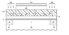
- a second photo-resist layer 316 is coated over the substrate 99 covering the gate stack layer 10 as shown in FIG. 3 e .
- the second photo-resist layer 316 is exposed using the second mask level 509 of FIG. 2 b , thereby forming second exposed regions 430 and second unexposed regions 431 .
- the second exposed regions 430 are developed as shown in FIG. 3 g . Further, the regions of the composite layer 311 are thus opened and also removed, for example, using a wet etch. Thus the printing assist features are removed during this step. Next, the second photo-resist layer 316 is etched off thus forming a patterned composite layer 311 that includes only the desired features. Next, as shown in FIG. 3 i , the pattern is transferred to gate stack layer 10 by a reactive ion etch. An additional trim etch may be performed at this stage to reduce the critical dimension of the gate stack layer 10 further, before removal of the composite layer 311 . Finally, as shown in FIG. 3 i , all the resist layers are removed forming the patterned gate stack layer 10 .
- gate stack formation further processing continues as per conventional flow. For example, spacers, extensions, source/drain regions, silicide regions, contacts and metallization including vias and metal lines may be formed completing the fabrication of the integrated circuit.
- FIG. 5 An embodiment of a method of manufacturing the integrated circuit will next be described using masks illustrated in FIG. 5 .
- the integrated circuit in various stages of manufacturing will then be described in FIG. 6 and the flow chart of FIG. 7 .
- FIGS. 5 a and 5 b provide illustrations of a mask used in the double patterning process to manufacture, for example, the transistor regions 200 (in FIG. 1 b ). Similar to FIG. 2 a , FIG. 5 a shows a third mask level 498 used in the formation of the first exposure.
- the first exposure comprises openings 500 in the mask exposing the photo-resist.
- the regions 501 are opaque to radiation and hence are not developed.
- the first exposure is used to pattern gate lines as well as form printing assist features.
- a second mask, as shown by the fourth mask level 508 over the transistor regions 200 (in FIG. 1 b ) exposes regions 510 selectively. Similar to the second mask level 509 , the fourth mask level 508 is an erase or cut mask in that it removes selected regions 510 .
- the fourth mask level 508 contains transparent mask regions 510 and opaque regions 511 that block exposure of any underlying resist.
- FIG. 5 b also illustrates the positioning of openings 500 (illustrated by dashed lines) from the third mask level 498 .
- the combination of the third and fourth exposure results in removal of printing assist features as described in various embodiments.
- FIGS. 6 a - 6 j provide cross-sectional diagrams illustrating an embodiment method of the present invention using the third mask level 498 and the fourth mask level 508 of FIG. 5 .
- FIG. 7 illustrates an associated flow diagram of one implementation of the process.
- isolation regions 26 including trenches 28 for isolation are formed in a substrate 99 .
- the top surface of the substrate 99 is subsequently polished and planarized.
- a gate dielectric 71 is deposited over exposed portions of the substrate 99 .
- a gate stack layer 10 is deposited over the gate dielectric 71 .
- the gate stack layer 10 preferably comprises a semiconductor material, such as polysilicon or amorphous silicon or a metallic layer.
- a composite layer 311 is deposited over the gate stack layer 10 .
- the composite layer 311 comprises oxide, nitrides, metals, or combinations thereof.
- Some examples of the composite layer 311 include silicon dioxide, silicon nitride, silicon oxy-nitride, titanium nitride, tantalum nitride, carbon, and silicon-carbon.
- a first planarizing layer 312 is coated over the composite layer 311 , and forms an anti-reflective coating layer.
- the first planarizing layer 312 also forms a planarized surface without additional polishing.
- an additional planarization step may be performed using, for example, a chemical mechanical polishing process.
- the first planarizing layer 312 preferably comprises a planarizing spin on material such as a bottom anti-reflective coating material (BARC).
- BARC bottom anti-reflective coating material
- the first planarizing layer 312 can also comprise another suitable organic underlayer of a trilayer resist stack used in advanced processing.
- the first dielectric layer 313 is coated over the first planarizing layer 312 .
- the first dielectric layer 313 comprises a spin on glass material and comprises silicon dioxide.
- the first dielectric layer 313 is coated at a low temperature to minimize damage of the underlying first planarizing layer 312 .
- a first photo-resist layer 315 is deposited on the first dielectric layer 313 .
- the first photo-resist layer 315 is a resist that can be developed by exposure to radiation and preferably by 193 nm or by 157 nm (or extreme UV) electromagnetic radiation.
- the resist used may either be positive or negative.
- Examples of resist polymers are poly-p-hydroxystyrene, acrylates, novolak or cycloaliphatic copolymers.
- the first photo-resist layer 315 is exposed using the third mask level 498 of FIG. 5 a .
- the third mask level 498 of FIG. 5 a comprises the desired gate features, but also includes the additional printing assist features. Thus, regions 420 are exposed whereas regions 421 remain unexposed.
- the first exposed regions 420 of the first photo-resist layer 315 are removed by etching.
- an anisotropic etch e.g., a reactive ion etch
- the etching to remove the first planarizing layer 312 may remove some or all the first photo-resist layer 315 .
- the composite layer 311 is etched.
- the patterned first photo-resist layer 315 (if remaining) is etched off.
- the first dielectric layer 313 and the first planarizing layer 312 are etched to expose the composite layer 311 .
- the composite layer 311 thus patterned comprises a template that includes patterns for forming both desired features 12 and printing assist features 11 .
- a second planarizing layer 317 is deposited over the composite layer 311 , as illustrated in FIG. 6 e .
- the second planarizing layer also fills in between the patterned composite layer 311 , in between the desired features 12 and the printing assist features 11 .
- the second planarizing layer 317 is preferably coated over the composite layer 311 to form a uniform surface.
- an additional planarization step may be performed using, for example, a chemical mechanical polishing process.
- the second planarizing layer 317 preferably comprises a dielectric that forms a uniform layer during the deposition process or during a subsequent process such as a thermal step.
- the second planarizing layer 317 preferably comprises a planarizing spin on material such as bottom anti-reflective coating materials (BARC).
- BARC bottom anti-reflective coating materials
- a second dielectric layer 318 is deposited over the second planarizing layer 317 .
- the second dielectric layer 318 is optional, and in different embodiments is a part of a trilayer stack.
- the second dielectric layer 318 comprises a spin on glass material and comprises silicon dioxide.
- the second dielectric layer 318 is coated at a low temperature to minimize damage of the underlying second planarizing layer 317 .
- a second photo-resist layer 316 is coated over the substrate 99 covering the second dielectric layer 318 as shown in FIG. 6 e .
- the second photo-resist layer 316 is exposed using the fourth mask level 508 of FIG. 5 b forming second exposed regions 430 and second unexposed regions 431 .
- the second exposed regions 430 are developed as shown in FIG. 6 g . Further, using the second unexposed regions 431 as a mask, the regions of the second dielectric layer 318 and the second planarizing layer 317 thus opened are also removed, for example, using a wet etch. Finally, the open regions of the composite layer 311 are removed. In some embodiments, a top portion of the gate stack layer 10 is also removed in this step, after removing the composite layer 311 . Thus, the printing assist features 11 are removed during this step. Next, any remaining second photo-resist layer 316 is stripped followed by removal of the second dielectric layer 318 and the second planarizing layer 317 . Thus forming a patterned composite layer 311 that includes only the desired features 12 ( FIG. 6 h ).
- the pattern is transferred to gate stack layer 10 by a reactive ion etching.
- the resist layers are removed forming the patterned gate stack layer 10 comprising the desired features 12 . Further processing continues as per conventional flow.
- FIG. 8 Another embodiment of a method of forming the integrated circuit using the double patterning technique is illustrated in FIG. 8 and the flow chart of FIG. 9 .
- This embodiment is similar to the embodiment illustrated in FIG. 6 , except the order of using the third mask level 498 and the fourth mask level 508 (of FIG. 5 ) is reversed. In particular, the fourth mask level 508 or erase mask is exposed before the third mask level 498 .
- FIG. 8 a hence illustrates an identical structure to that described in FIG. 6 a .
- the fourth mask level 508 is used to expose the first photo-resist layer 315 forming second exposed regions 430 and second unexposed regions 431 .
- the second exposed regions 430 are developed as shown in FIG. 8 c .
- the regions of the first dielectric layer 313 and the first planarizing layer 312 thus opened are also removed, for example, using a wet etch.
- the open regions of the composite layer 311 are removed ( FIG. 8 d ).
- a photo-resist layer is deposited again and exposed.
- a second planarizing layer 317 is coated over the substrate 99 covering the exposed gate stack layer 10 .
- a second dielectric layer 318 is deposited over the second planarizing layer 317 .
- a second photo-resist layer 316 is deposited over the second dielectric layer 318 .
- the second photo-resist layer 316 is exposed using the third mask level 498 of FIG. 5 b , again forming first exposed regions 420 and first unexposed regions 421 .
- the composite layer 311 is patterned.
- the first exposed regions 420 are developed as shown in FIG. 8 f .
- the regions of the second dielectric layer 318 and the second planarizing layer 317 thus opened are also removed, for example, using a wet etch.
- the open regions of the composite layer 311 are removed.
- the second photo-resist layer 316 (if remaining) is removed.
- the second dielectric layer 318 and the second planarizing layer 317 are removed forming a pattern on the composite layer 311 comprising only the desired features. Further processing continues as described, for example, in FIG. 3 h.
- an etch step was used to transfer the image before the second exposure step on the composite layer 311 (e.g., in FIG. 6 c ).
- the two exposure steps may be performed concurrently without an intermediate etch step.
- the final image is formed on the photo-resist by the combination of the first exposure and second exposure processes.
- FIG. 10 describes a final layout generated with designs optimally designed for each mask layer of the double patterning process.
- FIG. 10 a illustrates an overlay of two masks used in the double patterning process.
- opaque regions 501 on a fifth mask level 497 comprise desired features 12 including gate line 121 and uncritical features 122 , as well as printing assist features 11 .
- the printing assist features 11 are additional features and may comprise physical extensions of the desired features 12 .
- An erase mask or a sixth mask level 507 removes the printing assist features 11 .
- the gate line 121 is typically surrounded by contacts in the source and drain regions.
- the sixth mask level 507 needs to be aligned in such a manner that the printing assist features 11 are removed without removing the gate lines 121 .
- a distance “a” from the last gate line 121 to the edge of transparent regions 510 on the sixth mask level 507 is maximized without minimizing a distance “b” from the edge of the transparent regions 510 on the sixth mask level 507 to the last printing assist feature 111 .
- Such an optimization is necessary for producing sufficient space for placement of contacts.
- FIG. 10 b illustrates opaque regions 501 on the fifth mask level 497 and transparent regions 510 on the sixth mask level 507 (erase mask). Also illustrated are the desired features 12 including gate line 121 and uncritical features 122 , as well as printing assist features 11 .
- desired features 12 including gate line 121 and uncritical features 122 , as well as printing assist features 11 .
- various embodiments using the double patterning process form square line ends 721 .
- adjacent line ends can be brought closer.
- gate lines near the line ends 721 tend to shrink or neck and form regions over the active silicon without a gate line or with a smaller gate length, thus shorting the device.
- longer lines are used to avoid the deleterious effects of necking.
- the use of the erase mask as described in various embodiments of the invention avoids necking, as extended gate lines 720 are patterned with the exposed mask, which are later removed by the erase mask.
- the corner rounding 722 of the gate lines is significantly reduced, improving the margin for contacts landing on the gate lines.
- necking at line ends stays safely outside active area.
- the erase mask comprises cut features, which are features of different sizes and shapes.
- the cut features comprise a two dimensional shape, wherein at least one of the sides of the two dimensional shape is smaller in length than a parallel opposite side.
- Specific examples as illustrated in FIG. 10 b include a “T” or “L” shaped cut feature.
- the shape, size and placement of these cut features are optimized with respect to critical line width features (e.g., gate line 121 ), the placement of the printing assist features (e.g., printing assist features 11 ), and adjacent uncritical linewidth features (e.g., uncritical features 122 ).
- the cut features comprise features formed over extended desired features 12 for reducing line end shortening (e.g., extended gate lines 720 or line ends 721 ).
- the cut features also comprise T-type structures 723 for removing printing assist features 11 that connect to uncritical features 122 , and significantly reduce corner rounding 722 .
- FIG. 11 illustrates a top view of gate lines fabricated over a substrate, wherein FIGS. 11 a and 11 c illustrate gate lines formed in a single exposure and FIGS. 11 b and 11 d illustrate gate lines formed in accordance with embodiments of the invention.
- FIG. 11 e illustrates a magnified schematic of some of these distinctions for a single line formed in accordance with embodiments of the invention.
- FIG. 11 illustrates some of the key differences between a single exposure process and a double patterning process in accordance with embodiments of the invention.
- the line ends of FIGS. 11 b and 11 d show no corner rounding or necking whereas the line ends of FIGS. 11 a and 11 c illustrate both.
- the line ends of tips of FIGS. 11 b and 11 d illustrate sharp corners and tips.
- FIG. 11 e illustrate the rounded corners and line ends of first lines 791 processed with single exposure compared with sharp corners and tips for second lines 792 processed using embodiments of the present invention.
- FIG. 12 which includes FIG. 12 a - 12 e , illustrates an embodiment of the invention using multiple mask levels for either forming the desired features and the print assist features, or multiple mask levels for forming the cut shapes.
- the first reticle 777 comprising features for forming desired features 12 as well as for forming printing assist features 11 .
- the printing assist features 11 are the additional features.
- a second reticle 778 is used sequentially along with the first reticle 777 .
- the second reticle 778 may contain identical features to the first reticle 777 ; however, the features on the second reticle 778 are laterally displaced relative to the features on the first reticle 777 .
- the desired features 12 on the second reticle 778 are laterally displaced by a distance “c” relative to the desired features 12 on the first reticle 777 .
- a two reticle set is used for pitch doubling by splitting the pitch into two masks, so that each mask patterns a larger minimum feature than the final patterned structure.
- the wafer is processed, for example, as described in previous embodiments with respect to FIG. 6 a - 6 d .
- a second reticle 778 is used and the patterning process repeated.
- the wafer comprises the desired features 12 and the printing assist features 11 as illustrated in FIG. 12 c .
- this process can be extended to more number of reticles in various embodiments.
- a third reticle 787 comprising the cut features 797 is used to remove a portion of the printing assist features 11 .
- a fourth reticle 788 comprising the cut features 797 removes another portion of the printing assist features 11 .
- Each of the third reticles 787 and 787 follows the process described in earlier embodiments (for example FIGS. 6 e - 6 h ).
- a final pattern of the composite layer 311 comprising only the desired features 12 is formed.
Abstract
Description
Claims (26)
Priority Applications (1)
| Application Number | Priority Date | Filing Date | Title |
|---|---|---|---|
| US12/126,741 US8039203B2 (en) | 2007-09-25 | 2008-05-23 | Integrated circuits and methods of design and manufacture thereof |
Applications Claiming Priority (2)
| Application Number | Priority Date | Filing Date | Title |
|---|---|---|---|
| US11/860,955 US7785946B2 (en) | 2007-09-25 | 2007-09-25 | Integrated circuits and methods of design and manufacture thereof |
| US12/126,741 US8039203B2 (en) | 2007-09-25 | 2008-05-23 | Integrated circuits and methods of design and manufacture thereof |
Related Parent Applications (1)
| Application Number | Title | Priority Date | Filing Date |
|---|---|---|---|
| US11/860,955 Continuation-In-Part US7785946B2 (en) | 2007-09-25 | 2007-09-25 | Integrated circuits and methods of design and manufacture thereof |
Publications (2)
| Publication Number | Publication Date |
|---|---|
| US20090081563A1 US20090081563A1 (en) | 2009-03-26 |
| US8039203B2 true US8039203B2 (en) | 2011-10-18 |
Family
ID=40472010
Family Applications (1)
| Application Number | Title | Priority Date | Filing Date |
|---|---|---|---|
| US12/126,741 Expired - Fee Related US8039203B2 (en) | 2007-09-25 | 2008-05-23 | Integrated circuits and methods of design and manufacture thereof |
Country Status (1)
| Country | Link |
|---|---|
| US (1) | US8039203B2 (en) |
Cited By (2)
| Publication number | Priority date | Publication date | Assignee | Title |
|---|---|---|---|---|
| US8455354B2 (en) * | 2011-04-06 | 2013-06-04 | Taiwan Semiconductor Manufacturing Company, Ltd. | Layouts of POLY cut openings overlapping active regions |
| US8884342B2 (en) * | 2012-08-29 | 2014-11-11 | Infineon Technologies Ag | Semiconductor device with a passivation layer |
Families Citing this family (14)
| Publication number | Priority date | Publication date | Assignee | Title |
|---|---|---|---|---|
| KR100948464B1 (en) * | 2007-12-28 | 2010-03-17 | 주식회사 하이닉스반도체 | Method of forming patterns in semiconductor device |
| JP2009295785A (en) * | 2008-06-05 | 2009-12-17 | Toshiba Corp | Method of manufacturing semiconductor device |
| US7883829B2 (en) * | 2008-08-01 | 2011-02-08 | International Business Machines Corporation | Lithography for pitch reduction |
| US7994060B2 (en) * | 2009-09-01 | 2011-08-09 | International Business Machines Corporation | Dual exposure track only pitch split process |
| US8048764B2 (en) * | 2009-09-30 | 2011-11-01 | Taiwan Semiconductor Manufacturing Co., Ltd. | Dual etch method of defining active area in semiconductor device |
| US8159009B2 (en) * | 2009-11-19 | 2012-04-17 | Qualcomm Incorporated | Semiconductor device having strain material |
| US8875063B2 (en) | 2010-10-11 | 2014-10-28 | International Business Machines Corporation | Mask layout formation |
| US8298953B2 (en) * | 2010-12-20 | 2012-10-30 | Infineon Technologies Ag | Method for defining a separating structure within a semiconductor device |
| US8365108B2 (en) | 2011-01-06 | 2013-01-29 | International Business Machines Corporation | Generating cut mask for double-patterning process |
| FR2972293A1 (en) * | 2011-03-04 | 2012-09-07 | St Microelectronics Crolles 2 | METHOD FOR MANUFACTURING AN INTEGRATED CIRCUIT ON THE FORMATION OF LINES AND SLICES |
| EP2570854B1 (en) | 2011-09-16 | 2016-11-30 | Imec | Illumination-source shape definition in optical lithography |
| CN103633026A (en) * | 2012-08-23 | 2014-03-12 | 中芯国际集成电路制造(上海)有限公司 | Semiconductor device structure and manufacturing method thereof |
| KR102185281B1 (en) * | 2014-01-09 | 2020-12-01 | 삼성전자 주식회사 | Methods of Fabricating Patterns of Semiconductor Devices Using Self-Aligned Double Patterning Processes |
| US11354481B2 (en) * | 2018-06-29 | 2022-06-07 | Taiwan Semiconductor Manufacturing Company, Ltd. | Phase shifter circuit, phase shifter layout and method of forming the same |
Citations (13)
| Publication number | Priority date | Publication date | Assignee | Title |
|---|---|---|---|---|
| US5308741A (en) | 1992-07-31 | 1994-05-03 | Motorola, Inc. | Lithographic method using double exposure techniques, mask position shifting and light phase shifting |
| US5563012A (en) | 1994-06-30 | 1996-10-08 | International Business Machines Corporation | Multi mask method for selective mask feature enhancement |
| US5821014A (en) | 1997-02-28 | 1998-10-13 | Microunity Systems Engineering, Inc. | Optical proximity correction method for intermediate-pitch features using sub-resolution scattering bars on a mask |
| US20010020878A1 (en) | 1999-08-17 | 2001-09-13 | Speidell James L. | Encapsulated mems band-pass filter for integrated circuits |
| US6421820B1 (en) | 1999-12-13 | 2002-07-16 | Infineon Technologies Ag | Semiconductor device fabrication using a photomask with assist features |
| US20040063038A1 (en) * | 2002-04-18 | 2004-04-01 | Taiwan Semiconductor Manufacturing Co. | New method to reduce CD non-uniformity in IC manufacturing |
| US6734762B2 (en) | 2001-04-09 | 2004-05-11 | Motorola, Inc. | MEMS resonators and method for manufacturing MEMS resonators |
| US6777147B1 (en) | 2003-05-21 | 2004-08-17 | International Business Machines Corporation | Method for evaluating the effects of multiple exposure processes in lithography |
| US6787469B2 (en) | 2001-12-28 | 2004-09-07 | Texas Instruments Incorporated | Double pattern and etch of poly with hard mask |
| US6929887B1 (en) | 2002-04-18 | 2005-08-16 | Taiwan Semiconductor Manufacturing Co., Ltd. | Printable assist lines and the removal of such |
| US20060264001A1 (en) * | 2004-08-31 | 2006-11-23 | Luan Tran | Structures with increased photo-alignment margins |
| US20080014684A1 (en) | 2006-07-07 | 2008-01-17 | Texas Instruments, Incorporated. | Two-print-two-etch method for enhancement of CD control using ghost poly |
| US7495294B2 (en) * | 2005-12-21 | 2009-02-24 | Sandisk Corporation | Flash devices with shared word lines |
Family Cites Families (2)
| Publication number | Priority date | Publication date | Assignee | Title |
|---|---|---|---|---|
| US6862501B2 (en) * | 2002-10-28 | 2005-03-01 | Honeywell International Inc. | Method for producing 3D perspective view avionics terrain displays |
| US7623589B2 (en) * | 2006-07-14 | 2009-11-24 | Intel Corporation | Cooperative multiple-access using user-clustering and space-time-frequency coding techniques for higher reliability reception |
-
2008
- 2008-05-23 US US12/126,741 patent/US8039203B2/en not_active Expired - Fee Related
Patent Citations (13)
| Publication number | Priority date | Publication date | Assignee | Title |
|---|---|---|---|---|
| US5308741A (en) | 1992-07-31 | 1994-05-03 | Motorola, Inc. | Lithographic method using double exposure techniques, mask position shifting and light phase shifting |
| US5563012A (en) | 1994-06-30 | 1996-10-08 | International Business Machines Corporation | Multi mask method for selective mask feature enhancement |
| US5821014A (en) | 1997-02-28 | 1998-10-13 | Microunity Systems Engineering, Inc. | Optical proximity correction method for intermediate-pitch features using sub-resolution scattering bars on a mask |
| US20010020878A1 (en) | 1999-08-17 | 2001-09-13 | Speidell James L. | Encapsulated mems band-pass filter for integrated circuits |
| US6421820B1 (en) | 1999-12-13 | 2002-07-16 | Infineon Technologies Ag | Semiconductor device fabrication using a photomask with assist features |
| US6734762B2 (en) | 2001-04-09 | 2004-05-11 | Motorola, Inc. | MEMS resonators and method for manufacturing MEMS resonators |
| US6787469B2 (en) | 2001-12-28 | 2004-09-07 | Texas Instruments Incorporated | Double pattern and etch of poly with hard mask |
| US20040063038A1 (en) * | 2002-04-18 | 2004-04-01 | Taiwan Semiconductor Manufacturing Co. | New method to reduce CD non-uniformity in IC manufacturing |
| US6929887B1 (en) | 2002-04-18 | 2005-08-16 | Taiwan Semiconductor Manufacturing Co., Ltd. | Printable assist lines and the removal of such |
| US6777147B1 (en) | 2003-05-21 | 2004-08-17 | International Business Machines Corporation | Method for evaluating the effects of multiple exposure processes in lithography |
| US20060264001A1 (en) * | 2004-08-31 | 2006-11-23 | Luan Tran | Structures with increased photo-alignment margins |
| US7495294B2 (en) * | 2005-12-21 | 2009-02-24 | Sandisk Corporation | Flash devices with shared word lines |
| US20080014684A1 (en) | 2006-07-07 | 2008-01-17 | Texas Instruments, Incorporated. | Two-print-two-etch method for enhancement of CD control using ghost poly |
Non-Patent Citations (6)
| Title |
|---|
| Haffner, H., et al., "Mastering Double Exposure Process Window Aware OPC by Means of Virtual Targets," Proceedings of SPIE, Conference Proceedings Paper, vol. 6349, Oct. 20, 2006, 11 pages. |
| Meiring, J. E., et al., "ACLV Driven Double-Patterning Decomposition with Extensively Added Printing Assist Features (PrAFs)," Proceedings of SPIE, Conference Proceedings Paper, vol. 6520, Mar. 26, 2007, 12 pages. |
| Miller, S., et al., "Lithography Value Drivers in IC Design & Manufacturing," Semiconductor Fabtech-30TH Edition, Aug. 25, 2006, pp. 76-83. |
| Miller, S., et al., "Lithography Value Drivers in IC Design & Manufacturing," Semiconductor Fabtech—30TH Edition, Aug. 25, 2006, pp. 76-83. |
| Rabkin, P., et al., "Fabless/Foundry DFM: 45nm and Beyond," Semiconductor Fabtech-32ND Edition, Dec. 20, 2006, pp. 76-82. |
| Rabkin, P., et al., "Fabless/Foundry DFM: 45nm and Beyond," Semiconductor Fabtech—32ND Edition, Dec. 20, 2006, pp. 76-82. |
Cited By (3)
| Publication number | Priority date | Publication date | Assignee | Title |
|---|---|---|---|---|
| US8455354B2 (en) * | 2011-04-06 | 2013-06-04 | Taiwan Semiconductor Manufacturing Company, Ltd. | Layouts of POLY cut openings overlapping active regions |
| US8884342B2 (en) * | 2012-08-29 | 2014-11-11 | Infineon Technologies Ag | Semiconductor device with a passivation layer |
| US9859395B2 (en) | 2012-08-29 | 2018-01-02 | Infineon Technologies Ag | Semiconductor device with a passivation layer |
Also Published As
| Publication number | Publication date |
|---|---|
| US20090081563A1 (en) | 2009-03-26 |
Similar Documents
| Publication | Publication Date | Title |
|---|---|---|
| US8039203B2 (en) | Integrated circuits and methods of design and manufacture thereof | |
| US10089430B2 (en) | Integrated circuits and methods of design and manufacture thereof | |
| US11462408B2 (en) | Method of forming an integrated circuit using a patterned mask layer | |
| US8754530B2 (en) | Self-aligned borderless contacts for high density electronic and memory device integration | |
| US20060177977A1 (en) | Method for patterning fins and gates in a FinFET device using trimmed hard-mask capped with imaging layer | |
| US9202710B2 (en) | Method for defining a separating structure within a semiconductor device | |
| US8329592B2 (en) | Method of fabricating semiconductor device, and photomask | |
| US20140295650A1 (en) | Method for fabricating patterned structure of semiconductor device | |
| JP2003124339A (en) | Semiconductor device and its manufacturing method | |
| US10217633B2 (en) | Substantially defect-free polysilicon gate arrays | |
| US20090305506A1 (en) | Self-aligned dual patterning integration scheme | |
| CN112086433A (en) | Semiconductor element and method for manufacturing the same | |
| US8349528B2 (en) | Semiconductor devices and methods of manufacturing thereof | |
| US8211774B2 (en) | Method for forming semiconductor structure | |
| KR101780124B1 (en) | Semiconductor device with dummy gate structures | |
| TWI406325B (en) | Method for fabrication semiconductor structure |
Legal Events
| Date | Code | Title | Description |
|---|---|---|---|
| AS | Assignment |
Owner name: INFINEON TECHNOLOGIES NORTH AMERICA CORP., CALIFOR Free format text: ASSIGNMENT OF ASSIGNORS INTEREST;ASSIGNORS:HAFFNER, HENNING;ZHUANG, HAOREN;HEROLD, KLAUS;REEL/FRAME:021069/0177 Effective date: 20080515 |
|
| AS | Assignment |
Owner name: INTERNATIONAL BUSINESS MACHINES CORPORATION, NEW Y Free format text: ASSIGNMENT OF ASSIGNORS INTEREST;ASSIGNORS:WANG, HELEN;HALLE, SCOTT D.;COLBURN, MATTHEW E.;AND OTHERS;REEL/FRAME:021084/0491;SIGNING DATES FROM 20080515 TO 20080522 Owner name: INFINEON TECHNOLOGIES AG, GERMANY Free format text: ASSIGNMENT OF ASSIGNORS INTEREST;ASSIGNOR:INFINEON TECHNOLOGIES NORTH AMERICA CORP.;REEL/FRAME:021084/0508 Effective date: 20080612 Owner name: INFINEON TECHNOLOGIES AG,GERMANY Free format text: ASSIGNMENT OF ASSIGNORS INTEREST;ASSIGNOR:INFINEON TECHNOLOGIES NORTH AMERICA CORP.;REEL/FRAME:021084/0508 Effective date: 20080612 Owner name: INTERNATIONAL BUSINESS MACHINES CORPORATION, NEW Y Free format text: ASSIGNMENT OF ASSIGNORS INTEREST;ASSIGNORS:WANG, HELEN;HALLE, SCOTT D.;COLBURN, MATTHEW E.;AND OTHERS;SIGNING DATES FROM 20080515 TO 20080522;REEL/FRAME:021084/0491 |
|
| FEPP | Fee payment procedure |
Free format text: PAYOR NUMBER ASSIGNED (ORIGINAL EVENT CODE: ASPN); ENTITY STATUS OF PATENT OWNER: LARGE ENTITY |
|
| ZAAA | Notice of allowance and fees due |
Free format text: ORIGINAL CODE: NOA |
|
| ZAAB | Notice of allowance mailed |
Free format text: ORIGINAL CODE: MN/=. |
|
| STCF | Information on status: patent grant |
Free format text: PATENTED CASE |
|
| CC | Certificate of correction | ||
| FPAY | Fee payment |
Year of fee payment: 4 |
|
| MAFP | Maintenance fee payment |
Free format text: PAYMENT OF MAINTENANCE FEE, 8TH YEAR, LARGE ENTITY (ORIGINAL EVENT CODE: M1552); ENTITY STATUS OF PATENT OWNER: LARGE ENTITY Year of fee payment: 8 |
|
| FEPP | Fee payment procedure |
Free format text: MAINTENANCE FEE REMINDER MAILED (ORIGINAL EVENT CODE: REM.); ENTITY STATUS OF PATENT OWNER: LARGE ENTITY |
|
| LAPS | Lapse for failure to pay maintenance fees |
Free format text: PATENT EXPIRED FOR FAILURE TO PAY MAINTENANCE FEES (ORIGINAL EVENT CODE: EXP.); ENTITY STATUS OF PATENT OWNER: LARGE ENTITY |
|
| STCH | Information on status: patent discontinuation |
Free format text: PATENT EXPIRED DUE TO NONPAYMENT OF MAINTENANCE FEES UNDER 37 CFR 1.362 |
|
| FP | Lapsed due to failure to pay maintenance fee |
Effective date: 20231018 |