US8025204B2 - Method of wire bond encapsulation profiling - Google Patents
Method of wire bond encapsulation profiling Download PDFInfo
- Publication number
- US8025204B2 US8025204B2 US11/860,538 US86053807A US8025204B2 US 8025204 B2 US8025204 B2 US 8025204B2 US 86053807 A US86053807 A US 86053807A US 8025204 B2 US8025204 B2 US 8025204B2
- Authority
- US
- United States
- Prior art keywords
- encapsulant
- bead
- die
- mounting area
- microns
- Prior art date
- Legal status (The legal status is an assumption and is not a legal conclusion. Google has not performed a legal analysis and makes no representation as to the accuracy of the status listed.)
- Active, expires
Links
- 238000000034 method Methods 0.000 title claims abstract description 46
- 238000005538 encapsulation Methods 0.000 title description 3
- 239000008393 encapsulating agent Substances 0.000 claims abstract description 146
- 239000011324 bead Substances 0.000 claims abstract description 119
- 238000000151 deposition Methods 0.000 claims abstract description 7
- 239000004020 conductor Substances 0.000 claims description 54
- 239000000463 material Substances 0.000 claims description 23
- 239000004593 Epoxy Substances 0.000 claims description 16
- 229920000106 Liquid crystal polymer Polymers 0.000 claims description 14
- 239000004977 Liquid-crystal polymers (LCPs) Substances 0.000 claims description 14
- 238000000465 moulding Methods 0.000 claims description 7
- 230000009974 thixotropic effect Effects 0.000 claims description 6
- UFNIBRDIUNVOMX-UHFFFAOYSA-N 2,4'-dichlorobiphenyl Chemical compound C1=CC(Cl)=CC=C1C1=CC=CC=C1Cl UFNIBRDIUNVOMX-UHFFFAOYSA-N 0.000 description 7
- 230000004888 barrier function Effects 0.000 description 6
- 239000000758 substrate Substances 0.000 description 4
- 238000007598 dipping method Methods 0.000 description 3
- XUIMIQQOPSSXEZ-UHFFFAOYSA-N Silicon Chemical compound [Si] XUIMIQQOPSSXEZ-UHFFFAOYSA-N 0.000 description 2
- 238000004140 cleaning Methods 0.000 description 2
- 238000012423 maintenance Methods 0.000 description 2
- 230000009467 reduction Effects 0.000 description 2
- 229910052710 silicon Inorganic materials 0.000 description 2
- 239000010703 silicon Substances 0.000 description 2
- 238000005482 strain hardening Methods 0.000 description 2
- 238000012360 testing method Methods 0.000 description 2
- 238000010420 art technique Methods 0.000 description 1
- 239000000919 ceramic Substances 0.000 description 1
- 238000013461 design Methods 0.000 description 1
- 230000001627 detrimental effect Effects 0.000 description 1
- 239000000428 dust Substances 0.000 description 1
- 230000000694 effects Effects 0.000 description 1
- 230000005489 elastic deformation Effects 0.000 description 1
- 230000003028 elevating effect Effects 0.000 description 1
- 238000005530 etching Methods 0.000 description 1
- 239000011521 glass Substances 0.000 description 1
- 238000004519 manufacturing process Methods 0.000 description 1
- 230000007246 mechanism Effects 0.000 description 1
- 239000002184 metal Substances 0.000 description 1
- 238000012986 modification Methods 0.000 description 1
- 230000004048 modification Effects 0.000 description 1
- 238000004806 packaging method and process Methods 0.000 description 1
- 230000008569 process Effects 0.000 description 1
- 230000000630 rising effect Effects 0.000 description 1
- 239000004065 semiconductor Substances 0.000 description 1
- 238000007493 shaping process Methods 0.000 description 1
- 239000007787 solid Substances 0.000 description 1
Images


Classifications
-
- H—ELECTRICITY
- H01—ELECTRIC ELEMENTS
- H01L—SEMICONDUCTOR DEVICES NOT COVERED BY CLASS H10
- H01L21/00—Processes or apparatus adapted for the manufacture or treatment of semiconductor or solid state devices or of parts thereof
- H01L21/02—Manufacture or treatment of semiconductor devices or of parts thereof
- H01L21/04—Manufacture or treatment of semiconductor devices or of parts thereof the devices having at least one potential-jump barrier or surface barrier, e.g. PN junction, depletion layer or carrier concentration layer
- H01L21/50—Assembly of semiconductor devices using processes or apparatus not provided for in a single one of the subgroups H01L21/06 - H01L21/326, e.g. sealing of a cap to a base of a container
- H01L21/56—Encapsulations, e.g. encapsulation layers, coatings
-
- B—PERFORMING OPERATIONS; TRANSPORTING
- B41—PRINTING; LINING MACHINES; TYPEWRITERS; STAMPS
- B41J—TYPEWRITERS; SELECTIVE PRINTING MECHANISMS, i.e. MECHANISMS PRINTING OTHERWISE THAN FROM A FORME; CORRECTION OF TYPOGRAPHICAL ERRORS
- B41J2/00—Typewriters or selective printing mechanisms characterised by the printing or marking process for which they are designed
- B41J2/005—Typewriters or selective printing mechanisms characterised by the printing or marking process for which they are designed characterised by bringing liquid or particles selectively into contact with a printing material
- B41J2/01—Ink jet
- B41J2/135—Nozzles
- B41J2/14—Structure thereof only for on-demand ink jet heads
-
- B—PERFORMING OPERATIONS; TRANSPORTING
- B41—PRINTING; LINING MACHINES; TYPEWRITERS; STAMPS
- B41J—TYPEWRITERS; SELECTIVE PRINTING MECHANISMS, i.e. MECHANISMS PRINTING OTHERWISE THAN FROM A FORME; CORRECTION OF TYPOGRAPHICAL ERRORS
- B41J2/00—Typewriters or selective printing mechanisms characterised by the printing or marking process for which they are designed
- B41J2/005—Typewriters or selective printing mechanisms characterised by the printing or marking process for which they are designed characterised by bringing liquid or particles selectively into contact with a printing material
- B41J2/01—Ink jet
- B41J2/135—Nozzles
- B41J2/16—Production of nozzles
- B41J2/1621—Manufacturing processes
- B41J2/1623—Manufacturing processes bonding and adhesion
-
- H—ELECTRICITY
- H01—ELECTRIC ELEMENTS
- H01L—SEMICONDUCTOR DEVICES NOT COVERED BY CLASS H10
- H01L21/00—Processes or apparatus adapted for the manufacture or treatment of semiconductor or solid state devices or of parts thereof
- H01L21/67—Apparatus specially adapted for handling semiconductor or electric solid state devices during manufacture or treatment thereof; Apparatus specially adapted for handling wafers during manufacture or treatment of semiconductor or electric solid state devices or components ; Apparatus not specifically provided for elsewhere
- H01L21/67005—Apparatus not specifically provided for elsewhere
- H01L21/67011—Apparatus for manufacture or treatment
- H01L21/67126—Apparatus for sealing, encapsulating, glassing, decapsulating or the like
-
- H—ELECTRICITY
- H01—ELECTRIC ELEMENTS
- H01L—SEMICONDUCTOR DEVICES NOT COVERED BY CLASS H10
- H01L23/00—Details of semiconductor or other solid state devices
- H01L23/12—Mountings, e.g. non-detachable insulating substrates
- H01L23/13—Mountings, e.g. non-detachable insulating substrates characterised by the shape
-
- H—ELECTRICITY
- H01—ELECTRIC ELEMENTS
- H01L—SEMICONDUCTOR DEVICES NOT COVERED BY CLASS H10
- H01L23/00—Details of semiconductor or other solid state devices
- H01L23/28—Encapsulations, e.g. encapsulating layers, coatings, e.g. for protection
- H01L23/31—Encapsulations, e.g. encapsulating layers, coatings, e.g. for protection characterised by the arrangement or shape
- H01L23/3157—Partial encapsulation or coating
-
- H—ELECTRICITY
- H01—ELECTRIC ELEMENTS
- H01L—SEMICONDUCTOR DEVICES NOT COVERED BY CLASS H10
- H01L24/00—Arrangements for connecting or disconnecting semiconductor or solid-state bodies; Methods or apparatus related thereto
-
- H—ELECTRICITY
- H01—ELECTRIC ELEMENTS
- H01L—SEMICONDUCTOR DEVICES NOT COVERED BY CLASS H10
- H01L24/00—Arrangements for connecting or disconnecting semiconductor or solid-state bodies; Methods or apparatus related thereto
- H01L24/01—Means for bonding being attached to, or being formed on, the surface to be connected, e.g. chip-to-package, die-attach, "first-level" interconnects; Manufacturing methods related thereto
- H01L24/42—Wire connectors; Manufacturing methods related thereto
- H01L24/47—Structure, shape, material or disposition of the wire connectors after the connecting process
- H01L24/48—Structure, shape, material or disposition of the wire connectors after the connecting process of an individual wire connector
-
- H—ELECTRICITY
- H01—ELECTRIC ELEMENTS
- H01L—SEMICONDUCTOR DEVICES NOT COVERED BY CLASS H10
- H01L24/00—Arrangements for connecting or disconnecting semiconductor or solid-state bodies; Methods or apparatus related thereto
- H01L24/74—Apparatus for manufacturing arrangements for connecting or disconnecting semiconductor or solid-state bodies
- H01L24/78—Apparatus for connecting with wire connectors
-
- H—ELECTRICITY
- H01—ELECTRIC ELEMENTS
- H01L—SEMICONDUCTOR DEVICES NOT COVERED BY CLASS H10
- H01L24/00—Arrangements for connecting or disconnecting semiconductor or solid-state bodies; Methods or apparatus related thereto
- H01L24/80—Methods for connecting semiconductor or other solid state bodies using means for bonding being attached to, or being formed on, the surface to be connected
- H01L24/85—Methods for connecting semiconductor or other solid state bodies using means for bonding being attached to, or being formed on, the surface to be connected using a wire connector
-
- B—PERFORMING OPERATIONS; TRANSPORTING
- B41—PRINTING; LINING MACHINES; TYPEWRITERS; STAMPS
- B41J—TYPEWRITERS; SELECTIVE PRINTING MECHANISMS, i.e. MECHANISMS PRINTING OTHERWISE THAN FROM A FORME; CORRECTION OF TYPOGRAPHICAL ERRORS
- B41J2/00—Typewriters or selective printing mechanisms characterised by the printing or marking process for which they are designed
- B41J2/005—Typewriters or selective printing mechanisms characterised by the printing or marking process for which they are designed characterised by bringing liquid or particles selectively into contact with a printing material
- B41J2/01—Ink jet
- B41J2/135—Nozzles
- B41J2/14—Structure thereof only for on-demand ink jet heads
- B41J2002/14491—Electrical connection
-
- H—ELECTRICITY
- H01—ELECTRIC ELEMENTS
- H01L—SEMICONDUCTOR DEVICES NOT COVERED BY CLASS H10
- H01L2224/00—Indexing scheme for arrangements for connecting or disconnecting semiconductor or solid-state bodies and methods related thereto as covered by H01L24/00
- H01L2224/01—Means for bonding being attached to, or being formed on, the surface to be connected, e.g. chip-to-package, die-attach, "first-level" interconnects; Manufacturing methods related thereto
- H01L2224/42—Wire connectors; Manufacturing methods related thereto
- H01L2224/44—Structure, shape, material or disposition of the wire connectors prior to the connecting process
- H01L2224/45—Structure, shape, material or disposition of the wire connectors prior to the connecting process of an individual wire connector
- H01L2224/45001—Core members of the connector
- H01L2224/4501—Shape
- H01L2224/45012—Cross-sectional shape
- H01L2224/45015—Cross-sectional shape being circular
-
- H—ELECTRICITY
- H01—ELECTRIC ELEMENTS
- H01L—SEMICONDUCTOR DEVICES NOT COVERED BY CLASS H10
- H01L2224/00—Indexing scheme for arrangements for connecting or disconnecting semiconductor or solid-state bodies and methods related thereto as covered by H01L24/00
- H01L2224/01—Means for bonding being attached to, or being formed on, the surface to be connected, e.g. chip-to-package, die-attach, "first-level" interconnects; Manufacturing methods related thereto
- H01L2224/42—Wire connectors; Manufacturing methods related thereto
- H01L2224/47—Structure, shape, material or disposition of the wire connectors after the connecting process
- H01L2224/48—Structure, shape, material or disposition of the wire connectors after the connecting process of an individual wire connector
- H01L2224/4805—Shape
- H01L2224/4809—Loop shape
- H01L2224/48091—Arched
-
- H—ELECTRICITY
- H01—ELECTRIC ELEMENTS
- H01L—SEMICONDUCTOR DEVICES NOT COVERED BY CLASS H10
- H01L2224/00—Indexing scheme for arrangements for connecting or disconnecting semiconductor or solid-state bodies and methods related thereto as covered by H01L24/00
- H01L2224/01—Means for bonding being attached to, or being formed on, the surface to be connected, e.g. chip-to-package, die-attach, "first-level" interconnects; Manufacturing methods related thereto
- H01L2224/42—Wire connectors; Manufacturing methods related thereto
- H01L2224/47—Structure, shape, material or disposition of the wire connectors after the connecting process
- H01L2224/48—Structure, shape, material or disposition of the wire connectors after the connecting process of an individual wire connector
- H01L2224/481—Disposition
- H01L2224/48151—Connecting between a semiconductor or solid-state body and an item not being a semiconductor or solid-state body, e.g. chip-to-substrate, chip-to-passive
- H01L2224/48221—Connecting between a semiconductor or solid-state body and an item not being a semiconductor or solid-state body, e.g. chip-to-substrate, chip-to-passive the body and the item being stacked
- H01L2224/48225—Connecting between a semiconductor or solid-state body and an item not being a semiconductor or solid-state body, e.g. chip-to-substrate, chip-to-passive the body and the item being stacked the item being non-metallic, e.g. insulating substrate with or without metallisation
- H01L2224/48227—Connecting between a semiconductor or solid-state body and an item not being a semiconductor or solid-state body, e.g. chip-to-substrate, chip-to-passive the body and the item being stacked the item being non-metallic, e.g. insulating substrate with or without metallisation connecting the wire to a bond pad of the item
-
- H—ELECTRICITY
- H01—ELECTRIC ELEMENTS
- H01L—SEMICONDUCTOR DEVICES NOT COVERED BY CLASS H10
- H01L2224/00—Indexing scheme for arrangements for connecting or disconnecting semiconductor or solid-state bodies and methods related thereto as covered by H01L24/00
- H01L2224/01—Means for bonding being attached to, or being formed on, the surface to be connected, e.g. chip-to-package, die-attach, "first-level" interconnects; Manufacturing methods related thereto
- H01L2224/42—Wire connectors; Manufacturing methods related thereto
- H01L2224/47—Structure, shape, material or disposition of the wire connectors after the connecting process
- H01L2224/48—Structure, shape, material or disposition of the wire connectors after the connecting process of an individual wire connector
- H01L2224/484—Connecting portions
- H01L2224/4847—Connecting portions the connecting portion on the bonding area of the semiconductor or solid-state body being a wedge bond
- H01L2224/48472—Connecting portions the connecting portion on the bonding area of the semiconductor or solid-state body being a wedge bond the other connecting portion not on the bonding area also being a wedge bond, i.e. wedge-to-wedge
-
- H—ELECTRICITY
- H01—ELECTRIC ELEMENTS
- H01L—SEMICONDUCTOR DEVICES NOT COVERED BY CLASS H10
- H01L2224/00—Indexing scheme for arrangements for connecting or disconnecting semiconductor or solid-state bodies and methods related thereto as covered by H01L24/00
- H01L2224/74—Apparatus for manufacturing arrangements for connecting or disconnecting semiconductor or solid-state bodies and for methods related thereto
- H01L2224/78—Apparatus for connecting with wire connectors
-
- H—ELECTRICITY
- H01—ELECTRIC ELEMENTS
- H01L—SEMICONDUCTOR DEVICES NOT COVERED BY CLASS H10
- H01L2224/00—Indexing scheme for arrangements for connecting or disconnecting semiconductor or solid-state bodies and methods related thereto as covered by H01L24/00
- H01L2224/80—Methods for connecting semiconductor or other solid state bodies using means for bonding being attached to, or being formed on, the surface to be connected
- H01L2224/85—Methods for connecting semiconductor or other solid state bodies using means for bonding being attached to, or being formed on, the surface to be connected using a wire connector
- H01L2224/85909—Post-treatment of the connector or wire bonding area
- H01L2224/8592—Applying permanent coating, e.g. protective coating
-
- H—ELECTRICITY
- H01—ELECTRIC ELEMENTS
- H01L—SEMICONDUCTOR DEVICES NOT COVERED BY CLASS H10
- H01L2224/00—Indexing scheme for arrangements for connecting or disconnecting semiconductor or solid-state bodies and methods related thereto as covered by H01L24/00
- H01L2224/80—Methods for connecting semiconductor or other solid state bodies using means for bonding being attached to, or being formed on, the surface to be connected
- H01L2224/85—Methods for connecting semiconductor or other solid state bodies using means for bonding being attached to, or being formed on, the surface to be connected using a wire connector
- H01L2224/85909—Post-treatment of the connector or wire bonding area
- H01L2224/8593—Reshaping, e.g. for severing the wire, modifying the wedge or ball or the loop shape
- H01L2224/85947—Reshaping, e.g. for severing the wire, modifying the wedge or ball or the loop shape by mechanical means, e.g. "pull-and-cut", pressing, stamping
-
- H—ELECTRICITY
- H01—ELECTRIC ELEMENTS
- H01L—SEMICONDUCTOR DEVICES NOT COVERED BY CLASS H10
- H01L23/00—Details of semiconductor or other solid state devices
- H01L23/48—Arrangements for conducting electric current to or from the solid state body in operation, e.g. leads, terminal arrangements ; Selection of materials therefor
- H01L23/488—Arrangements for conducting electric current to or from the solid state body in operation, e.g. leads, terminal arrangements ; Selection of materials therefor consisting of soldered or bonded constructions
- H01L23/495—Lead-frames or other flat leads
- H01L23/49517—Additional leads
- H01L23/4952—Additional leads the additional leads being a bump or a wire
-
- H—ELECTRICITY
- H01—ELECTRIC ELEMENTS
- H01L—SEMICONDUCTOR DEVICES NOT COVERED BY CLASS H10
- H01L2924/00—Indexing scheme for arrangements or methods for connecting or disconnecting semiconductor or solid-state bodies as covered by H01L24/00
- H01L2924/0001—Technical content checked by a classifier
- H01L2924/00014—Technical content checked by a classifier the subject-matter covered by the group, the symbol of which is combined with the symbol of this group, being disclosed without further technical details
-
- H—ELECTRICITY
- H01—ELECTRIC ELEMENTS
- H01L—SEMICONDUCTOR DEVICES NOT COVERED BY CLASS H10
- H01L2924/00—Indexing scheme for arrangements or methods for connecting or disconnecting semiconductor or solid-state bodies as covered by H01L24/00
- H01L2924/01—Chemical elements
- H01L2924/01014—Silicon [Si]
-
- H—ELECTRICITY
- H01—ELECTRIC ELEMENTS
- H01L—SEMICONDUCTOR DEVICES NOT COVERED BY CLASS H10
- H01L2924/00—Indexing scheme for arrangements or methods for connecting or disconnecting semiconductor or solid-state bodies as covered by H01L24/00
- H01L2924/01—Chemical elements
- H01L2924/01027—Cobalt [Co]
-
- H—ELECTRICITY
- H01—ELECTRIC ELEMENTS
- H01L—SEMICONDUCTOR DEVICES NOT COVERED BY CLASS H10
- H01L2924/00—Indexing scheme for arrangements or methods for connecting or disconnecting semiconductor or solid-state bodies as covered by H01L24/00
- H01L2924/01—Chemical elements
- H01L2924/01033—Arsenic [As]
-
- H—ELECTRICITY
- H01—ELECTRIC ELEMENTS
- H01L—SEMICONDUCTOR DEVICES NOT COVERED BY CLASS H10
- H01L2924/00—Indexing scheme for arrangements or methods for connecting or disconnecting semiconductor or solid-state bodies as covered by H01L24/00
- H01L2924/095—Indexing scheme for arrangements or methods for connecting or disconnecting semiconductor or solid-state bodies as covered by H01L24/00 with a principal constituent of the material being a combination of two or more materials provided in the groups H01L2924/013 - H01L2924/0715
- H01L2924/097—Glass-ceramics, e.g. devitrified glass
- H01L2924/09701—Low temperature co-fired ceramic [LTCC]
-
- H—ELECTRICITY
- H01—ELECTRIC ELEMENTS
- H01L—SEMICONDUCTOR DEVICES NOT COVERED BY CLASS H10
- H01L2924/00—Indexing scheme for arrangements or methods for connecting or disconnecting semiconductor or solid-state bodies as covered by H01L24/00
- H01L2924/10—Details of semiconductor or other solid state devices to be connected
- H01L2924/102—Material of the semiconductor or solid state bodies
- H01L2924/1025—Semiconducting materials
- H01L2924/10251—Elemental semiconductors, i.e. Group IV
- H01L2924/10253—Silicon [Si]
-
- H—ELECTRICITY
- H01—ELECTRIC ELEMENTS
- H01L—SEMICONDUCTOR DEVICES NOT COVERED BY CLASS H10
- H01L2924/00—Indexing scheme for arrangements or methods for connecting or disconnecting semiconductor or solid-state bodies as covered by H01L24/00
- H01L2924/10—Details of semiconductor or other solid state devices to be connected
- H01L2924/11—Device type
- H01L2924/14—Integrated circuits
-
- H—ELECTRICITY
- H01—ELECTRIC ELEMENTS
- H01L—SEMICONDUCTOR DEVICES NOT COVERED BY CLASS H10
- H01L2924/00—Indexing scheme for arrangements or methods for connecting or disconnecting semiconductor or solid-state bodies as covered by H01L24/00
- H01L2924/10—Details of semiconductor or other solid state devices to be connected
- H01L2924/146—Mixed devices
- H01L2924/1461—MEMS
-
- H—ELECTRICITY
- H01—ELECTRIC ELEMENTS
- H01L—SEMICONDUCTOR DEVICES NOT COVERED BY CLASS H10
- H01L2924/00—Indexing scheme for arrangements or methods for connecting or disconnecting semiconductor or solid-state bodies as covered by H01L24/00
- H01L2924/20—Parameters
- H01L2924/207—Diameter ranges
- H01L2924/20753—Diameter ranges larger or equal to 30 microns less than 40 microns
Definitions
- the invention relates to the field of integrated circuit packaging.
- the encapsulation of the wire bonds between a circuit board and the contact pads on the integrated circuit die is particularly advantageous.
- Integrated circuits fabricated on silicon wafer substrates are electrically connected to printed circuit boards by wire bonds.
- the wire bonds are very thin wires—around 25 to 40 microns in diameter—extending from contact pads along the side of the wafer substrate to contacts on the printed circuit board (PCB).
- PCB printed circuit board
- encapsulant To protect and strengthen the wire bonds, they are sealed within a bead of epoxy called encapsulant.
- the wires from the contact pads to the PCB are made longer than necessary to accommodate changes in the gap between the PCB and the contact pads because of thermal expansion, flex in the components and so on. These longer than necessary wires naturally form an arc between the contact pads and the PCB.
- the top of the wire arc is often about 300 microns above the contact pads although some wire bonding may extend even higher.
- the encapsulant needs to encapsulate the full length of the wire so the encapsulant bead will extend 500 microns to 600 microns proud of the contact pads.
- the integrated circuit fabricated on the silicon wafer is often referred to as a ‘die’.
- die will be used as a reference to an integrated circuit fabricated on a wafer substrate using lithographic the well known etching and deposition techniques commonly used in semiconductor fabrication. If the die is purely an electronic microprocessor, there is little need to keep close control of the encapsulant bead dimensions. However, if the die is a micro-electro mechanical systems (MEMS) device with an active upper surface, it may be necessary or desirable to bring the active surface of the die onto close proximity with another surface.
- MEMS micro-electro mechanical systems
- Inkjet printheads The proximity of the print media to the nozzle array influences the print quality. Similarly, if a cleaning surface is wiped across the nozzles, the bead of encapsulant can hamper the wiping contact.
- the present invention provides a microprocessor device comprising:
- a support structure having a chip mounting area and a conductor mounting area
- the die having a back surface in contact with the chip mounting area and an active surface opposing the back surface, the active surface having electrical contact pads;
- the chip mounting area is raised relative to the conductor mounting area.
- the top of the arc formed by the layer is much closer to the active surface of the die. This, in turn, allows the bead of encapsulant to have a lower profile relative to the active surface. With a lower encapsulant bead, the active surface can be brought into closer proximity with another surface without making contact.
- the nozzle array on a printhead IC can be 300 microns to 400 microns from the paper path.
- the chip mounting area is raised more than 100 microns relative to the conductor mounting area.
- the support structure has a step between the chip mounting area and the conductor mounting area.
- the plurality of conductors are incorporated into a flexible printed circuit board (flex PCB) with a line of bond pads along an edge closest the die, the bond pads being more than 2 mm from the contacts pads on the die.
- flex PCB flexible printed circuit board
- the wire bonds are formed from wire with a diameter less than 40 microns and extend less than 100 microns above the active surface of the die.
- the wire bonds are plastically deformed such that they extend less than 50 microns above the active surface of the die.
- the active surface has functional elements spaced less than 260 microns from the contacts pads of the die.
- the die is an inkjet printhead IC and the functional elements are nozzles through which ink is ejected.
- the support structure is a liquid crystal polymer (LCP) molding.
- the wire bonds are covered in a bead of encapsulant, the bead of encapsulant extending less than 200 microns above the active surface of the die.
- the wire bonds are covered in a bead of encapsulant, the bead of encapsulant having a profiled surface that is flat, parallel to and spaced less than 100 microns from the active surface.
- the wire bonds are covered in a bead of encapsulant, the bead of encapsulant having a profiled surface that is flat and inclined relative to the active surface.
- the wire bonds are covered in a bead of encapsulant, the encapsulant being an epoxy material that is thixotropic when uncured.
- the wire bonds are covered in a bead of encapsulant, the encapsulant being an epoxy material has a viscosity greater than 700 cp when uncured.
- the printhead IC is mounted in a printer such that during use the nozzles are less than 100 microns from the paper path.
- the present invention provides a method of profiling a wire bond between a contact pad on a die, and a conductor on a supporting structure, the method comprising the steps of:
- the strength of the wire bond is known to be relatively small; of the order of 3 to 5 grams force.
- the Applicant's work has found that the wire bond structure is robust enough to withstand a certain degree of work hardening from plastic deformation. The arc of the wire bond can be deformed into a flatter profile without compromising the electrical connection with the PCB.
- the die has an active surface that has functional elements, the contacts pad being formed at one edge of the active surface, the wire bond has a diameter less than 40 microns and the arc extends more than 100 microns above the active surface of the die.
- the wire bond is plastically deformed such that it extends less than 50 microns above the active surface of the die.
- the wire bond is pushed by engagement with a blade having a rounded edge section for contacting the wire bond.
- the bead of encapsulant having a profiled surface that is flat and inclined relative to the active surface.
- the encapsulant being an epoxy material has a viscosity greater than 700 cp when uncured.
- the encapsulant being an epoxy material that is thixotropic when uncured.
- the method further comprises the steps of:
- the active surface has functional elements spaced less than 260 microns from the contacts pads of the die.
- the die is an inkjet printhead IC and the functional elements are nozzles through which ink is ejected.
- the printhead IC is mounted in a printer such that during use the nozzles are less than 100 microns from the paper path.
- the support structure has a chip mounting area and a conductor mounting area, the die is supported on the chip mounting area, and a plurality of electrical conductors at least partially supported on the conductor mounting area wherein, the chip mounting area is raised relative to the conductor mounting area.
- the chip mounting area is raised more than 100 microns relative to the conductor mounting area.
- the support structure has a step between the chip mounting area and the conductor mounting area.
- the plurality of conductors are incorporated into a flexible printed circuit board (flex PCB) with a line of bond pads along an edge closest the die, the bond pads being more than 2 mm from the contacts pads on the die.
- flex PCB flexible printed circuit board
- the support structure is a liquid crystal polymer (LCP) molding.
- LCP liquid crystal polymer
- the present invention provides a method for profiling a bead of encapsulant extending along an edge of a die mounted to a supporting structure, the method comprising the steps of:
- the encapsulant can be effectively shaped by a profiling surface without stripping the encapsulant from the wire bonds.
- the normally convex-shaped upper surface of the encapsulant bead can be pushed to one side of the bead with the profiling surface.
- the active surface With a lower encapsulant bead, the active surface can be brought into closer proximity with another surface without making contact.
- the nozzle array on a printhead IC can be 300 microns to 400 microns from the paper path.
- the nozzle array on the printhead IC can be less than 100 microns from the paper path.
- the wire bonds extend in an arc from respective contact pads on the die to corresponding conductors on the support structure and the method further comprises the steps of:
- the die has an active surface that has functional elements, the contacts pad being formed at one edge of the active surface, the wire bond has a diameter less than 40 microns and the arc extends more than 100 microns above the active surface of the die.
- the wire bond is plastically deformed such that it extends less than 50 microns above the active surface of the die.
- the wire bond is pushed by engagement with a blade having a rounded edge section for contacting the wire bond.
- the bead of encapsulant has a profiled surface that is flat, parallel to and spaced less than 100 microns from the active surface.
- the bead of encapsulant has a profiled surface that is flat and inclined relative to the active surface.
- the encapsulant being an epoxy material has a viscosity greater than 700 cp when uncured.
- the encapsulant being an epoxy material that is thixotropic when uncured.
- the method further comprises the steps of:
- the active surface has functional elements spaced less than 260 microns from the contacts pads of the die.
- the die is an inkjet printhead IC and the functional elements are nozzles through which ink is ejected.
- the printhead IC is mounted in a printer such that during use the nozzles are less than 100 microns from the paper path.
- the support structure has a chip mounting area and a conductor mounting area, the die is supported on the chip mounting area, and a plurality of electrical conductors at least partially supported on the conductor mounting area wherein, the chip mounting area is raised relative to the conductor mounting area.
- the chip mounting area is raised more than 100 microns relative to the conductor mounting area.
- the support structure has a step between the chip mounting area and the conductor mounting area.
- the plurality of conductors are incorporated into a flexible printed circuit board (flex PCB) with a line of bond pads along an edge closest the die, the bond pads being more than 2 mm from the contacts pads on the die.
- flex PCB flexible printed circuit board
- the support structure is a liquid crystal polymer (LCP) molding.
- LCP liquid crystal polymer
- the present invention provides a method of applying encapsulant to a die mounted to a support structure, the method comprising the steps of:
- the die having a back surface in contact with the support structure and an active surface opposing the back surface, the active surface having electrical contact pads;
- a barrier over the active surface so that it defines a narrow gap allows the geometry of the encapsulant front (the line of contact between the encapsulant and the active surface) can be more closely controlled. Any variation in the flowrate of encapsulant from the needle tends to cause bulges or valleys in the height of the bead and or the PCB side of the bead.
- the fluidic resistance generated by the gap between the barrier and the active surface means that the amount of encapsulant that flows into the gap and onto the active surface is almost constant.
- the reduced flow variations make the encapsulant front closely correspond to the shape of the barrier. Greater control of the encapsulant front allows the functional elements of the active surface of the die to be closer to the contact pads.
- the barrier is a profiling surface and the method further comprises the steps of:
- the method further comprises the steps of:
- the active surface that has functional elements, the contacts pad being formed at one edge of the active surface, the wire bond has a diameter less than 40 microns and the arc extends more than 100 microns above the active surface of the die.
- the wire bond is plastically deformed such that it extends less than 50 microns above the active surface of the die.
- the wire bond is pushed by engagement with a blade having a rounded edge section for contacting the wire bond.
- the bead of encapsulant has a profiled surface that is flat, parallel to and spaced less than 100 microns from the active surface.
- the bead of encapsulant has a profiled surface that is flat and inclined relative to the active surface.
- the encapsulant being an epoxy material has a viscosity greater than 700 cp when uncured.
- the encapsulant is an epoxy material that is thixotropic when uncured.
- the active surface has functional elements spaced less than 260 microns from the contacts pads of the die.
- the die is an inkjet printhead IC and the functional elements are nozzles through which ink is ejected.
- the printhead IC is mounted in a printer such that during use the nozzles are less than 100 microns from the paper path.
- the support structure has a chip mounting area and a conductor mounting area, the die is supported on the chip mounting area, and a plurality of electrical conductors at least partially supported on the conductor mounting area wherein, the chip mounting area is raised relative to the conductor mounting area.
- the chip mounting area is raised more than 100 microns relative to the conductor mounting area.
- the support structure has a step between the chip mounting area and the conductor mounting area.
- the plurality of conductors are incorporated into a flexible printed circuit board (flex PCB) with a line of bond pads along an edge closest the die, the bond pads being more than 2 mm from the contacts pads on the die.
- flex PCB flexible printed circuit board
- the support structure is a liquid crystal polymer (LCP) molding.
- LCP liquid crystal polymer
- the present invention provides a method of applying encapsulant to wire bonds between a die and conductors on a supporting substrate, the method comprising the steps of:
- Wiping the encapsulant over the wire bonds with a profiling surface provides control of the encapsulant front as well as the height of the encapsulant relative to the die.
- the movement of the profiling surface relative to the die can closely controlled to shape the encapsulant to a desired form.
- the encapsulant can be shaped to present an inclined face rising from the nozzle surface to a high point over the wire bonds. This can be used by the printhead maintenance facilities to maintain contact pressure on the wiping mechanism. This is illustrated further below with reference to the drawings.
- the encapsulant can be shaped to have ridges, gutters, grooves and so on by using a particular shape of profiling surface and relative movement with the die.
- the method further comprises the steps of:
- the profiling surface is a blade with a straight edge and the method further comprises the steps of:
- the die has an active surface with functional elements and a plurality of contacts pad being formed along one edge for connection with the wire bonds such that the wire bonds extend in an arc from the contacts pads to each of the conductors respectively, the wire bonds having a diameter less than 40 microns and the arc extends more than 100 microns above the active surface of the die.
- the method further comprises the steps of:
- the wire bond is plastically deformed such that it extends less than 50 microns above the active surface of the die.
- the wire bond is pushed by engagement with a blade having a rounded edge section for contacting the wire bond.
- the encapsulant covering the wire bonds has a profiled surface that is flat, parallel to and spaced less than 100 microns from the active surface.
- the bead of encapsulant having a profiled surface that is flat and inclined relative to the active surface.
- the encapsulant being an epoxy material has a viscosity greater than 700 cp when uncured.
- the encapsulant is an epoxy material that is thixotropic when uncured.
- the functional elements are spaced less than 260 microns from the contacts pads of the die.
- the die is an inkjet printhead IC and the functional elements are nozzles through which ink is ejected.
- the printhead IC is mounted in a printer such that during use the nozzles are less than 100 microns from the paper path.
- the support structure has a chip mounting area and a conductor mounting area, the die is supported on the chip mounting area, and a plurality of electrical conductors at least partially supported on the conductor mounting area wherein, the chip mounting area is raised relative to the conductor mounting area.
- the chip mounting area is raised more than 100 microns relative to the conductor mounting area.
- the support structure has a step between the chip mounting area and the conductor mounting area.
- the plurality of conductors are incorporated into a flexible printed circuit board (flex PCB) with a line of bond pads along an edge closest the die, the bond pads being more than 2 mm from the contacts pads on the die.
- the support structure is a liquid crystal polymer (LCP) molding.
- FIG. 1 is a schematic representation of a common prior art technique for applying a bead of encapsulant to wire bonds;
- FIG. 2 is a schematic representation of a die mounted to a supporting structure with a chip mounting area raised relative to the flex PCB mounting area;
- FIGS. 3A , 3 B and 3 C are schematic representations of the encapsulant bead being profiled into a desired shape using a moveable blade;
- FIGS. 4A to 4D are schematic representations of wire bonds being profiled by plastic deformation
- FIGS. 5A and 5B show the encapsulant bead height reductions for plastically deformed wire bonds
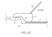
- FIGS. 6A to 6C show the encapsulant bead being applied to the wire bonds using the profiling blade.
- FIGS. 7A and 7B show the profiling blade being used to control the encapsulant bead front on the surface of the die.
- the wire bonds 16 are covered in a bead on encapsulant 2 to protect and reinforce the bonds.
- the encapsulant 2 is dispensed from a discharge needle 18 directly onto the wire bonds 16 .
- the encapsulant bead 2 is three separate beads—two beads of so-called ‘dam’ encapsulant 20 , and one bead of ‘fill’ encapsulant 22 .
- the dam encapsulant 20 has a higher viscosity than the fill encapsulant 22 , and serves to form a channel to hold the fill encapsulant bead.
- the height H of the bead 2 above the die 4 is usually about 500-600 microns. In most electronic devices, this does not pose a problem. However, if the die has an active surface that needs to operate in close proximity to another surface, this bead can be an obstruction.
- FIG. 2 shows a stepped support structure 6 that has raised the chip mounting area 26 relative to the PCB mounting area 24 (or at least the area mounting the PCB bonds pads 12 ).
- the arc of the wire bonds 16 are lower relative to active surface 28 of the die 4 .
- the end of the wire bond 16 attached to the contact pad 10 can be the apex of the arc (bearing in mind that the wire bond arc is intended to accommodate some relative movement of the die and PCB).
- the bead has a reduced height H above the active surface 28 of the die 4 .
- Bead heights less than 100 microns are easily achievable, and with additional measures, such as wire arc collapsing and bead profiling (discussed below), bead height of less than 50 microns are possible.
- the height of the wire bonds 16 above the die is about 34 microns.
- the wire bond height is around 20 microns. Raising the die even further has shown little or no further reduction in wire bond height with a step of 710 microns having a wire bond height of around 20 microns.
- FIGS. 3A to 3C show the encapsulant 2 being profiled with a profiling blade 30 .
- the support structure 6 is again stepped to reduce the height of the wire bonds 16 above the die 4 .
- the profiling blade 30 moves across the die 4 and wire bonds in a predetermined path.
- the blade 30 displaces the top of the bead 30 to its flex PCB side to form a flat top surface 32 that is at a significantly reduced height H above the die 4 .
- the relative movement of the blade 30 and the die 4 can be precisely controlled. This allows the height H to be determined by the tolerance of the wire bonding process. As long as H is greater than the nominal height of the wire bond arc above the die, plus the maximum tolerance, the encapsulant 2 will cover and protect the wire bonds 16 . With this technique, the height H can be easily reduced from 500-600 microns to less than 300 microns. If the heights of the wire bond arcs are also reduced, the height H of the encapsulant bead can be less than 100 microns. The Applicant uses this technique to profile encapsulant on printhead dies down to a height of 50 microns at its lowest point. As shown in FIG.
- the lowest point is at the encapsulant front and the blade 30 forms an inclined face 32 in the top of the bead 2 .
- the inclined face is utilized by the printhead maintenance system when cleaning the paper dust and dried ink from the nozzle face. This illustrates the technique's ability to not just reduce the height of the encapsulant bead, but to form a surface that can perform functions other than just encapsulate the wire bonds.
- the edge profile of the blade and the path of the blade relative to the die can be configured to form a surface that has a multitude of shapes for a variety of purposes.
- FIGS. 4A to 4C show another technique for lowering the profile of wire bonds.
- FIG. 4A shows the die 4 connected to the flex PCB 8 via the wire bonds 16 . While the stepped support structure 6 has lowered the height of the wire bond arcs compared to a flat supporting structure, the wire bonds still have a natural tendency to bow upwards rather than downwards towards the corner of the step.
- the wires 16 are typically about 32 microns in diameter and have a pull force of about 3 to 5 grams force. The pull force is the tensile load necessary to break the connection to the contact pad 10 or the bond pad 12 . Given the fragility of these structures (one of the reasons encapsulant is applied), conventional wisdom is to avoid any contact between the wire bond arcs and other solid surfaces.
- the arc of the wire bonds 16 can be collapsed by a wire pusher 34 .
- the wire pusher 34 displaces the wire bond 16 enough to elastically and plastically deform the arc.
- the Applicants have shown that contact with the wire pusher 34 can cause localized work hardening in the wire, but as long as the pushing force is not excessive, it does not break.
- the end of the wire pusher 34 is rounded to avoid stress concentration points.
- the wire pusher may be a stylus for engaging single wire bonds or a blade that pushes on multiple wire bonds simultaneously.
- FIGS. 6A , 6 B and 6 C show the application of the encapsulant bead using the profiling blade 30 instead of a discharge needle (see FIGS. 1 and 2 ).
- the flowrate of encapsulant from the discharge needle can vary and this gives rise to large variations on the position of the encapsulant front on the active surface of the die 4 . Consequently, any functional elements in the active surface of the die need to be sufficiently spaced from the contacts pads 10 to allow for the meandering encapsulant front.
- the bead of encapsulant 40 can be formed on the profiling blade 30 by simply dipping it into a reservoir of uncured encapsulant epoxy.
- the bead 40 may also be formed by any other convenient method, such as running the discharge needle along one end of the blade 30 .
- the wire bond 16 height has been reduced by collapsing the arc in accordance with the techniques discussed above.
- the bead 2 deposited by the discharge needle need not be as big to cover the wire bond 16 once it has been collapsed.
- the blade 30 can be brought closer to the die 4 without contacting wire bonds 16 when profiling the encapsulant 2 .
- the bead profile in FIG. 6C is substantially lower than that of FIG. 6B .
- the profiling blade 30 is used to control the front 36 of the bead of encapsulant 2 .
- the blade 30 is positioned over the die 4 to define a gap 42 between its lower edge and the active surface 28 .
- the discharge needle 18 dispenses the encapsulant material 44 , it flows onto the active surface, one side of the blade and a fillet of the material extends through the gap 42 . Because of the flow restriction created by the gap, flow variations have a reduced effect on the dimensions of the fillet that flows through the gap. Therefore the encapsulant front 36 closely corresponds to the line of the lower edge of the blade 30 .
- the profiling blade 30 is already in position to profile the encapsulant bead 2 once it has been dispensed from the discharge needle.
- the blade 30 simply moves over the die 4 in a direction away from the nozzles 38 . This keeps the encapsulant front 36 in place and flattens the profile of the encapsulant bead 2 over the wire bonds 16 .
Abstract
Description
| 11/860,539 | 11/860,540 | 11/860,541 | 11/860,542 | |
| 6,405,055 | 6,628,430 | 7,136,186 | 10/920,372 | 7,145,689 | 7,130,075 | 7,081,974 |
| 7,177,055 | 7,209,257 | 7,161,715 | 7,154,632 | 7,158,258 | 7,148,993 | 7,075,684 |
| 7,158,809 | 11/225,172 | 11/474,280 | 11/635,482 | 11/635,526 | 11/650,545 | 11/653,241 |
| 11/653,240 | 11,758,648 | 7,241,005 | 7,108,437 | 6,915,140 | 6,999,206 | 7,136,198 |
| 7,092,130 | 7,249,108 | 6,566,858 | 6,331,946 | 6,246,970 | 6,442,525 | 09/517,384 |
| 09/505,951 | 6,374,354 | 7,246,098 | 6,816,968 | 6,757,832 | 6,334,190 | 6,745,331 |
| 7,249,109 | 10/203,559 | 7,197,642 | 7,093,139 | 10/636,263 | 10/636,283 | 10/866,608 |
| 7,210,038 | 10/902,833 | 10/940,653 | 10/942,858 | 11/706,329 | 11/757,385 | 11/758,642 |
| 7,170,652 | 6,967,750 | 6,995,876 | 7,099,051 | 11/107,942 | 7,193,734 | 11/209,711 |
| 11/599,336 | 7,095,533 | 6,914,686 | 7,161,709 | 7,099,033 | 11/003,786 | 7,258,417 |
| 11/003,418 | 11/003,334 | 11/003,600 | 11/003,404 | 11/003,419 | 11/003,700 | 7,255,419 |
| 11/003,618 | 7,229,148 | 7,258,416 | 11/003,698 | 11/003,420 | 6,984,017 | 11/003,699 |
| 11/071,473 | 11,748,482 | 11/778,563 | 11/779,851 | 11/778,574 | 11/853,816 | 11/853,814 |
| 11/853,786 | 11/856,694 | 11/003,463 | 11/003,701 | 11/003,683 | 11/003,614 | 11/003,702 |
| 11/003,684 | 7,246,875 | 11/003,617 | 11/764,760 | 11,853,777 | 11/293,800 | 11/293,802 |
| 11/293,801 | 11/293,808 | 11/293,809 | 11/482,975 | 11/482,970 | 11/482,968 | 11/482,972 |
| 11/482,971 | 11/482,969 | 11/097,266 | 11/097,267 | 11/685,084 | 11/685,086 | 11/685,090 |
| 11/740,925 | 11/763,444 | 11/763,443 | 11/518,238 | 11/518,280 | 11/518,244 | 11/518,243 |
| 11/518,242 | 11/084,237 | 11/084,240 | 11/084,238 | 11/357,296 | 11/357,298 | 11/357,297 |
| 11/246,676 | 11/246,677 | 11/246,678 | 11/246,679 | 11/246,680 | 11/246,681 | 11/246,714 |
| 11/246,713 | 11/246,689 | 11/246,671 | 11/246,670 | 11/246,669 | 11/246,704 | 11/246,710 |
| 11/246,688 | 11/246,716 | 11/246,715 | 11/246,707 | 11/246,706 | 11/246,705 | 11/246,708 |
| 11/246,693 | 11/246,692 | 11/246,696 | 11/246,695 | 11/246,694 | 11/482,958 | 11/482,955 |
| 11/482,962 | 11/482,963 | 11/482,956 | 11/482,954 | 11/482,974 | 11/482,957 | 11/482,987 |
| 11/482,959 | 11/482,960 | 11/482,961 | 11/482,964 | 11/482,965 | 11/482,976 | 11/482,973 |
| 11/495,815 | 11/495,816 | 11/495,817 | 6,227,652 | 6,213,588 | 6,213,589 | 6,231,163 |
| 6,247,795 | 6,394,581 | 6,244,691 | 6,257,704 | 6,416,168 | 6,220,694 | 6,257,705 |
| 6,247,794 | 6,234,610 | 6,247,793 | 6,264,306 | 6,241,342 | 6,247,792 | 6,264,307 |
| 6,254,220 | 6,234,611 | 6,302,528 | 6,283,582 | 6,239,821 | 6,338,547 | 6,247,796 |
| 6,557,977 | 6,390,603 | 6,362,843 | 6,293,653 | 6,312,107 | 6,227,653 | 6,234,609 |
| 6,238,040 | 6,188,415 | 6,227,654 | 6,209,989 | 6,247,791 | 6,336,710 | 6,217,153 |
| 6,416,167 | 6,243,113 | 6,283,581 | 6,247,790 | 6,260,953 | 6,267,469 | 6,588,882 |
| 6,742,873 | 6,918,655 | 6,547,371 | 6,938,989 | 6,598,964 | 6,923,526 | 6,273,544 |
| 6,309,048 | 6,420,196 | 6,443,558 | 6,439,689 | 6,378,989 | 6,848,181 | 6,634,735 |
| 6,299,289 | 6,299,290 | 6,425,654 | 6,902,255 | 6,623,101 | 6,406,129 | 6,505,916 |
| 6,457,809 | 6,550,895 | 6,457,812 | 7,152,962 | 6,428,133 | 7,216,956 | 7,080,895 |
| 11/144,844 | 7,182,437 | 11/599,341 | 11/635,533 | 11/607,976 | 11/607,975 | 11/607,999 |
| 11/607,980 | 11/607,979 | 11/607,978 | 11/735,961 | 11/685,074 | 11/696,126 | 11/696,144 |
| 11/696,650 | 11/763,446 | 10/407,212 | 7,252,366 | 10/683,064 | 10/683,041 | 11,766,713 |
| 11/841,647 | 11/482,980 | 11/563,684 | 11/482,967 | 11/482,966 | 11/482,988 | 11/482,989 |
| 11/293,832 | 11/293,838 | 11/293,825 | 11/293,841 | 11/293,799 | 11/293,796 | 11/293,797 |
| 11/293,798 | 11/124,158 | 11/124,196 | 11/124,199 | 11/124,162 | 11/124,202 | 11/124,197 |
| 11/124,154 | 11/124,198 | 11/124,153 | 11/124,151 | 11/124,160 | 11/124,192 | 11/124,175 |
| 11/124,163 | 11/124,149 | 11/124,152 | 11/124,173 | 11/124,155 | 7,236,271 | 11/124,174 |
| 11/124,194 | 11/124,164 | 11/124,200 | 11/124,195 | 11/124,166 | 11/124,150 | 11/124,172 |
| 11/124,165 | 11/124,186 | 11/124,185 | 11/124,184 | 11/124,182 | 11/124,201 | 11/124,171 |
| 11/124,181 | 11/124,161 | 11/124,156 | 11/124,191 | 11/124,159 | 11/124,176 | 11/124,188 |
| 11/124,170 | 11/124,187 | 11/124,189 | 11/124,190 | 11/124,180 | 11/124,193 | 11/124,183 |
| 11/124,178 | 11/124,177 | 11/124,148 | 11/124,168 | 11/124,167 | 11/124,179 | 11/124,169 |
| 11/187,976 | 11/188,011 | 11/188,014 | 11/482,979 | 11/735,490 | 11/853,018 | 11/228,540 |
| 11/228,500 | 11/228,501 | 11/228,530 | 11/228,490 | 11/228,531 | 11/228,504 | 11/228,533 |
| 11/228,502 | 11/228,507 | 11/228,482 | 11/228,505 | 11/228,497 | 11/228,487 | 11/228,529 |
| 11/228,484 | 11/228,489 | 11/228,518 | 11/228,536 | 11/228,496 | 11/228,488 | 11/228,506 |
| 11/228,516 | 11/228,526 | 11/228,539 | 11/228,538 | 11/228,524 | 11/228,523 | 11/228,519 |
| 11/228,528 | 11/228,527 | 11/228,525 | 11/228,520 | 11/228,498 | 11/228,511 | 11/228,522 |
| 111/228,515 | 11/228,537 | 11/228,534 | 11/228,491 | 11/228,499 | 11/228,509 | 11/228,492 |
| 11/228,493 | 11/228,510 | 11/228,508 | 11/228,512 | 11/228,514 | 11/228,494 | 11/228,495 |
| 11/228,486 | 11/228,481 | 11/228,477 | 11/228,485 | 11/228,483 | 11/228,521 | 11/228,517 |
| 11/228,532 | 11/228,513 | 11/228,503 | 11/228,480 | 11/228,535 | 11/228,478 | 11/228,479 |
| 6,087,638 | 6,340,222 | 6,041,600 | 6,299,300 | 6,067,797 | 6,286,935 | 6,044,646 |
| 6,382,769 | 10/868,866 | 6,787,051 | 6,938,990 | 11/242,916 | 11/242,917 | 11/144,799 |
| 11/198,235 | 11/766,052 | 7,152,972 | 11/592,996 | 6,746,105 | 11/763,440 | 11/763,442 |
| 11/246,687 | 11/246,718 | 11/246,685 | 11/246,686 | 11/246,703 | 11/246,691 | 11/246,711 |
| 11/246,690 | 11/246,712 | 11/246,717 | 11/246,709 | 11/246,700 | 11/246,701 | 11/246,702 |
| 11/246,668 | 11/246,697 | 11/246,698 | 11/246,699 | 11/246,675 | 11/246,674 | 11/246,667 |
| 11/829,957 | 11/829,960 | 11/829,961 | 11/829,962 | 11/829,963 | 11/829,966 | 11/829,967 |
| 11/829,968 | 11/829,969 | 7,156,508 | 7,159,972 | 7,083,271 | 7,165,834 | 7,080,894 |
| 7,201,469 | 7,090,336 | 7,156,489 | 10/760,233 | 10/760,246 | 7,083,257 | 7,258,422 |
| 7,255,423 | 7,219,980 | 10/760,253 | 10/760,255 | 10/760,209 | 7,118,192 | 10/760,194 |
| 10/760,238 | 7,077,505 | 7,198,354 | 7,077,504 | 10/760,189 | 7,198,355 | 10/760,232 |
| 10/760,231 | 7,152,959 | 7,213,906 | 7,178,901 | 7,222,938 | 7,108,353 | 7,104,629 |
| 11/446,227 | 11/454,904 | 11/472,345 | 11/474,273 | 7,261,401 | 11/474,279 | 11/482,939 |
| 11/482,950 | 11/499,709 | 11/592,984 | 11/601,668 | 11/603,824 | 11/601,756 | 11/601,672 |
| 11/650,546 | 11/653,253 | 11/706,328 | 11/706,299 | 11/706,965 | 11/737,080 | 11/737,041 |
| 11/778,062 | 11/778,566 | 11,782,593 | 11/246,684 | 11/246,672 | 11/246,673 | 11/246,683 |
| 11/246,682 | 60/939,086 | 7,246,886 | 7,128,400 | 7,108,355 | 6,991,322 | 10/728,790 |
| 7,118,197 | 10/728,784 | 10/728,783 | 7,077,493 | 6,962,402 | 10/728,803 | 7,147,308 |
| 10/728,779 | 7,118,198 | 7,168,790 | 7,172,270 | 7,229,155 | 6,830,318 | 7,195,342 |
| 7,175,261 | 10/773,183 | 7,108,356 | 7,118,202 | 10/773,186 | 7,134,744 | 10/773,185 |
| 7,134,743 | 7,182,439 | 7,210,768 | 10/773,187 | 7,134,745 | 7,156,484 | 7,118,201 |
| 7,111,926 | 10/773,184 | 7,018,021 | 11/060,751 | 11/060,805 | 11/188,017 | 7,128,402 |
| 11/298,774 | 11/329,157 | 11/490,041 | 11/501,767 | 11/499,736 | 7,246,885 | 7,229,156 |
| 11/505,846 | 11/505,857 | 11/505,856 | 11/524,908 | 11/524,938 | 7,258,427 | 11/524,912 |
| 11/592,999 | 11/592,995 | 11/603,825 | 11/649,773 | 11/650,549 | 11/653,237 | 11/706,378 |
| 11/706,962 | 11,749,118 | 11/754,937 | 11,749,120 | 11/744,885 | 11/779,850 | 11/765,439 |
| 11,842,950 | 11/839,539 | 11/097,308 | 11/097,309 | 7,246,876 | 11/097,299 | 11/097,310 |
| 11/097,213 | 11/210,687 | 11/097,212 | 7,147,306 | 7,261,394 | 11/764,806 | 11/782,595 |
| 11/482,953 | 11/482,977 | 11/544,778 | 11/544,779 | 11/764,808 | 09/575,197 | 7,079,712 |
| 6,825,945 | 09/575,165 | 6,813,039 | 6,987,506 | 7,038,797 | 6,980,318 | 6,816,274 |
| 7,102,772 | 09/575,186 | 6,681,045 | 6,728,000 | 7,173,722 | 7,088,459 | 09/575,181 |
| 7,068,382 | 7,062,651 | 6,789,194 | 6,789,191 | 6,644,642 | 6,502,614 | 6,622,999 |
| 6,669,385 | 6,549,935 | 6,987,573 | 6,727,996 | 6,591,884 | 6,439,706 | 6,760,119 |
| 09/575,198 | 6,290,349 | 6,428,155 | 6,785,016 | 6,870,966 | 6,822,639 | 6,737,591 |
| 7,055,739 | 7,233,320 | 6,830,196 | 6,832,717 | 6,957,768 | 09/575,172 | 7,170,499 |
| 7,106,888 | 7,123,239 | 11/066,161 | 11/066,160 | 11/066,159 | 11/066,158 | 11/066,165 |
| 10/727,181 | 10/727,162 | 10/727,163 | 10/727,245 | 7,121,639 | 7,165,824 | 7,152,942 |
| 10/727,157 | 7,181,572 | 7,096,137 | 10/727,257 | 10/727,238 | 7,188,282 | 10/727,159 |
| 10/727,180 | 10/727,179 | 10/727,192 | 10/727,274 | 10/727,164 | 10/727,161 | 10/727,198 |
| 10/727,158 | 10/754,536 | 10/754,938 | 10/727,227 | 10/727,160 | 10/934,720 | 7,171,323 |
| 11/272,491 | 11/474,278 | 11/488,853 | 11/488,841 | 11,749,750 | 11,749,749 | 10/296,522 |
| 6,795,215 | 7,070,098 | 7,154,638 | 6,805,419 | 6,859,289 | 6,977,751 | 6,398,332 |
| 6,394,573 | 6,622,923 | 6,747,760 | 6,921,144 | 10/884,881 | 7,092,112 | 7,192,106 |
| 11/039,866 | 7,173,739 | 6,986,560 | 7,008,033 | 11/148,237 | 7,222,780 | 11/248,426 |
| 11/478,599 | 11/499,749 | 11/738,518 | 11/482,981 | 11/743,661 | 11/743,659 | 11/752,900 |
| 7,195,328 | 7,182,422 | 11/650,537 | 11/712,540 | 10/854,521 | 10/854,522 | 10/854,488 |
| 10/854,487 | 10/854,503 | 10/854,504 | 10/854,509 | 7,188,928 | 7,093,989 | 10/854,497 |
| 10/854,495 | 10/854,498 | 10/854,511 | 10/854,512 | 10/854,525 | 10/854,526 | 10/854,516 |
| 10/854,508 | 7,252,353 | 10/854,515 | 10/854,506 | 10/854,505 | 10/854,493 | 10/854,494 |
| 10/854,489 | 10/854,490 | 10/854,492 | 10/854,491 | 10/854,528 | 10/854,523 | 10/854,527 |
| 10/854,524 | 10/854,520 | 10/854,514 | 10/854,519 | 10/854,513 | 10/854,499 | 10/854,501 |
| 7,266,661 | 7,243,193 | 10/854,518 | 10/854,517 | 10/934,628 | 7,163,345 | 11/499,803 |
| 11/601,757 | 11/706,295 | 11/735,881 | 11,748,483 | 11,749,123 | 11/766,061 | 11,775,135 |
| 11,772,235 | 11/778,569 | 11/829,942 | 11/014,731 | 11/544,764 | 11/544,765 | 11/544,772 |
| 11/544,773 | 11/544,774 | 11/544,775 | 11/544,776 | 11/544,766 | 11/544,767 | 11/544,771 |
| 11/544,770 | 11/544,769 | 11/544,777 | 11/544,768 | 11/544,763 | 11/293,804 | 11/293,840 |
| 11/293,803 | 11/293,833 | 11/293,834 | 11/293,835 | 11/293,836 | 11/293,837 | 11/293,792 |
| 11/293,794 | 11/293,839 | 11/293,826 | 11/293,829 | 11/293,830 | 11/293,827 | 11/293,828 |
| 11/293,795 | 11/293,823 | 11/293,824 | 11/293,831 | 11/293,815 | 11/293,819 | 11/293,818 |
| 11/293,817 | 11/293,816 | 11/838,875 | 11/482,978 | 11/640,356 | 11/640,357 | 11/640,358 |
| 11/640,359 | 11/640,360 | 11/640,355 | 11/679,786 | 10/760,254 | 10/760,210 | 10/760,202 |
| 7,201,468 | 10/760,198 | 10/760,249 | 7,234,802 | 10/760,196 | 10/760,247 | 7,156,511 |
| 10/760,264 | 7,258,432 | 7,097,291 | 10/760,222 | 10/760,248 | 7,083,273 | 10/760,192 |
| 10/760,203 | 10/760,204 | 10/760,205 | 10/760,206 | 10/760,267 | 10/760,270 | 7,198,352 |
| 10/760,271 | 10/760,275 | 7,201,470 | 7,121,655 | 10/760,184 | 7,232,208 | 10/760,186 |
| 10/760,261 | 7,083,272 | 11/501,771 | 11/583,874 | 11/650,554 | 11/706,322 | 11/706,968 |
| 11/749,119 | 11,779,848 | 11/855,152 | 11,855,151 | 11/014,764 | 11/014,763 | 11/014,748 |
| 11/014,747 | 11/014,761 | 11/014,760 | 11/014,757 | 11/014,714 | 7,249,822 | 11/014,762 |
| 11/014,724 | 11/014,723 | 11/014,756 | 11/014,736 | 11/014,759 | 11/014,758 | 11/014,725 |
| 11/014,739 | 11/014,738 | 11/014,737 | 11/014,726 | 11/014,745 | 11/014,712 | 11/014,715 |
| 11/014,751 | 11/014,735 | 11/014,734 | 11/014,719 | 11/014,750 | 11/014,749 | 7,249,833 |
| 11/758,640 | 11/775,143 | 11/838,877 | 11/014,769 | 11/014,729 | 11/014,743 | 11/014,733 |
| 11/014,754 | 11/014,755 | 11/014,765 | 11/014,766 | 11/014,740 | 11/014,720 | 11/014,753 |
| 7,255,430 | 11/014,744 | 11/014,741 | 11/014,768 | 11/014,767 | 11/014,718 | 11/014,717 |
| 11/014,716 | 11/014,732 | 11/014,742 | 11/097,268 | 11/097,185 | 11/097,184 | 11/778,567 |
| 11,852,958 | 11,852,907 | 11/293,820 | 11/293,813 | 11/293,822 | 11/293,812 | 11/293,821 |
| 11/293,814 | 11/293,793 | 11/293,842 | 11/293,811 | 11/293,807 | 11/293,806 | 11/293,805 |
| 11/293,810 | 11/688,863 | 11/688,864 | 11/688,865 | 11/688,866 | 11/688,867 | 11/688,868 |
| 11/688,869 | 11/688,871 | 11/688,872 | 11/688,873 | 11/741,766 | 11/482,982 | 11/482,983 |
| 11/482,984 | 11/495,818 | 11/495,819 | 11/677,049 | 11/677,050 | 11/677,051 | 11/014,722 |
| 10/760,180 | 7,111,935 | 10/760,213 | 10/760,219 | 10/760,237 | 7,261,482 | 10/760,220 |
| 7,002,664 | 10/760,252 | 10/760,265 | 7,088,420 | 11/446,233 | 11/503,083 | 11/503,081 |
| 11/516,487 | 11/599,312 | 11/014,728 | 11/014,727 | 7,237,888 | 7,168,654 | 7,201,272 |
| 6,991,098 | 7,217,051 | 6,944,970 | 10/760,215 | 7,108,434 | 10/760,257 | 7,210,407 |
| 7,186,042 | 10/760,266 | 6,920,704 | 7,217,049 | 10/760,214 | 10/760,260 | 7,147,102 |
| 10/760,269 | 7,249,838 | 10/760,241 | 10/962,413 | 10/962,427 | 7,261,477 | 7,225,739 |
| 10/962,402 | 10/962,425 | 10/962,428 | 7,191,978 | 10/962,426 | 10/962,409 | 10/962,417 |
| 10/962,403 | 7,163,287 | 7,258,415 | 10/962,523 | 7,258,424 | 10/962,410 | 7,195,412 |
| 7,207,670 | 11/282,768 | 7,220,072 | 11/474,267 | 11/544,547 | 11/585,925 | 11/593,000 |
| 11/706,298 | 11/706,296 | 11/706,327 | 11/730,760 | 11/730,407 | 11/730,787 | 11/735,977 |
| 11/736,527 | 11/753,566 | 11/754,359 | 11/778,061 | 11/765,398 | 11/778,556 | 11/829,937 |
| 11/780,470 | 11/223,262 | 11/223,018 | 11/223,114 | 11/223,022 | 11/223,021 | 11/223,020 |
| 11/223,019 | 11/014,730 | 7,154,626 | 7,079,292 | 11/604,316 | ||
Claims (15)
Priority Applications (1)
| Application Number | Priority Date | Filing Date | Title |
|---|---|---|---|
| US11/860,538 US8025204B2 (en) | 2007-09-25 | 2007-09-25 | Method of wire bond encapsulation profiling |
Applications Claiming Priority (1)
| Application Number | Priority Date | Filing Date | Title |
|---|---|---|---|
| US11/860,538 US8025204B2 (en) | 2007-09-25 | 2007-09-25 | Method of wire bond encapsulation profiling |
Publications (2)
| Publication Number | Publication Date |
|---|---|
| US20090081818A1 US20090081818A1 (en) | 2009-03-26 |
| US8025204B2 true US8025204B2 (en) | 2011-09-27 |
Family
ID=40472097
Family Applications (1)
| Application Number | Title | Priority Date | Filing Date |
|---|---|---|---|
| US11/860,538 Active 2027-11-20 US8025204B2 (en) | 2007-09-25 | 2007-09-25 | Method of wire bond encapsulation profiling |
Country Status (1)
| Country | Link |
|---|---|
| US (1) | US8025204B2 (en) |
Cited By (2)
| Publication number | Priority date | Publication date | Assignee | Title |
|---|---|---|---|---|
| US20110316201A1 (en) * | 2010-06-24 | 2011-12-29 | Taiwan Semiconductor Manufacturing Company, Ltd. | Wafer Level Packaging Using Blade Molding |
| WO2017190926A1 (en) | 2016-05-02 | 2017-11-09 | Memjet Technology Limited | Monochrome inkjet printhead configured for high-speed printing |
Families Citing this family (2)
| Publication number | Priority date | Publication date | Assignee | Title |
|---|---|---|---|---|
| US8759138B2 (en) | 2008-02-11 | 2014-06-24 | Suncore Photovoltaics, Inc. | Concentrated photovoltaic system modules using III-V semiconductor solar cells |
| US9331228B2 (en) | 2008-02-11 | 2016-05-03 | Suncore Photovoltaics, Inc. | Concentrated photovoltaic system modules using III-V semiconductor solar cells |
Citations (29)
| Publication number | Priority date | Publication date | Assignee | Title |
|---|---|---|---|---|
| US4595938A (en) * | 1983-06-10 | 1986-06-17 | Ing. C. Olivetti & C., S.P.A. | Ink jet print head |
| US5008736A (en) | 1989-11-20 | 1991-04-16 | Motorola, Inc. | Thermal protection method for a power device |
| US5468999A (en) | 1994-05-26 | 1995-11-21 | Motorola, Inc. | Liquid encapsulated ball grid array semiconductor device with fine pitch wire bonding |
| US5577319A (en) | 1995-03-31 | 1996-11-26 | Motorola, Inc. | Method of encapsulating a crystal oscillator |
| US5863488A (en) * | 1995-09-22 | 1999-01-26 | Japan Gore-Tex Inc. | Molded article of liquid crystal polymer |
| US6022583A (en) | 1997-12-16 | 2000-02-08 | Nordson Corporation | Method of encapsulating a wire bonded die |
| US6071427A (en) | 1998-06-03 | 2000-06-06 | Lexmark International, Inc. | Method for making a printhead |
| US6143588A (en) | 1997-09-09 | 2000-11-07 | Amkor Technology, Inc. | Method of making an integrated circuit package employing a transparent encapsulant |
| US20010014486A1 (en) | 1999-06-03 | 2001-08-16 | Glenn Thomas P. | Method Of Making A Plastic Pakage For An Optical Integrated Circuit Device |
| US6291884B1 (en) * | 1999-11-09 | 2001-09-18 | Amkor Technology, Inc. | Chip-size semiconductor packages |
| US6326240B1 (en) * | 1998-12-31 | 2001-12-04 | World Wiser Electronics Inc. | Apparatus for packaging semiconductor device and method for packaging the same |
| US6414849B1 (en) | 1999-10-29 | 2002-07-02 | Stmicroelectronics, Inc. | Low stress and low profile cavity down flip chip and wire bond BGA package |
| WO2003006230A1 (en) | 2001-07-09 | 2003-01-23 | Nordson Corporation | Method and apparatus for underfilling electronic components using vacuum assist |
| US20030160311A1 (en) | 2002-02-28 | 2003-08-28 | Aminuddin Ismail | Stacked die semiconductor device |
| US6644782B1 (en) | 2002-05-23 | 2003-11-11 | Hewlett-Packard Development Company, L.P. | Printing system and printing under firing data resolution method for printing system |
| US6709893B2 (en) * | 1998-05-11 | 2004-03-23 | Micron Technology, Inc. | Interconnections for a semiconductor device and method for forming same |
| US6790473B2 (en) | 1995-10-26 | 2004-09-14 | International Business Machines Corporation | Lead protective coating composition, process and structure thereof |
| US6805541B1 (en) | 1999-02-15 | 2004-10-19 | Kabushiki Kaisha Toshiba | Resin encapsulating apparatus used in a manufacture of a semiconductor device |
| US20040241906A1 (en) * | 2003-05-28 | 2004-12-02 | Vincent Chan | Integrated circuit package and method for making same that employs under bump metalization layer |
| US6836962B2 (en) | 1993-11-16 | 2005-01-04 | Formfactor, Inc. | Method and apparatus for shaping spring elements |
| US6885093B2 (en) | 2002-02-28 | 2005-04-26 | Freescale Semiconductor, Inc. | Stacked die semiconductor device |
| US20050242159A1 (en) * | 2004-04-28 | 2005-11-03 | Texas Instruments Incorporated | System and method for low loop wire bonding |
| US20070045872A1 (en) | 2005-08-31 | 2007-03-01 | Fee Setho S | Microelectronic devices having intermediate contacts for connection to interposer substrates, and associated methods of packaging microelectronic devices with intermediate contacts |
| US20070105280A1 (en) | 2005-11-09 | 2007-05-10 | Freescale Semiconductor, Inc. | Brace for wire loop |
| US20080099895A1 (en) | 2006-10-27 | 2008-05-01 | Samsung Techwin Co., Ltd. | Semiconductor package and method of forming wire loop of semiconductor package |
| US20080158298A1 (en) | 2006-12-28 | 2008-07-03 | Serbicki Jeffrey P | Printhead wirebond encapsulation |
| US20080237887A1 (en) * | 2007-03-29 | 2008-10-02 | Hem Takiar | Semiconductor die stack having heightened contact for wire bond |
| US20090032926A1 (en) * | 2007-07-31 | 2009-02-05 | Advanced Micro Devices, Inc. | Integrated Support Structure for Stacked Semiconductors With Overhang |
| US7669751B2 (en) * | 2007-09-25 | 2010-03-02 | Silverbrook Research Pty Ltd | Method of forming low profile wire bonds between integrated circuits dies and printed circuit boards |
-
2007
- 2007-09-25 US US11/860,538 patent/US8025204B2/en active Active
Patent Citations (30)
| Publication number | Priority date | Publication date | Assignee | Title |
|---|---|---|---|---|
| US4595938A (en) * | 1983-06-10 | 1986-06-17 | Ing. C. Olivetti & C., S.P.A. | Ink jet print head |
| US5008736A (en) | 1989-11-20 | 1991-04-16 | Motorola, Inc. | Thermal protection method for a power device |
| US6836962B2 (en) | 1993-11-16 | 2005-01-04 | Formfactor, Inc. | Method and apparatus for shaping spring elements |
| US5468999A (en) | 1994-05-26 | 1995-11-21 | Motorola, Inc. | Liquid encapsulated ball grid array semiconductor device with fine pitch wire bonding |
| US5577319A (en) | 1995-03-31 | 1996-11-26 | Motorola, Inc. | Method of encapsulating a crystal oscillator |
| US5863488A (en) * | 1995-09-22 | 1999-01-26 | Japan Gore-Tex Inc. | Molded article of liquid crystal polymer |
| US6790473B2 (en) | 1995-10-26 | 2004-09-14 | International Business Machines Corporation | Lead protective coating composition, process and structure thereof |
| US6143588A (en) | 1997-09-09 | 2000-11-07 | Amkor Technology, Inc. | Method of making an integrated circuit package employing a transparent encapsulant |
| US6022583A (en) | 1997-12-16 | 2000-02-08 | Nordson Corporation | Method of encapsulating a wire bonded die |
| US6709893B2 (en) * | 1998-05-11 | 2004-03-23 | Micron Technology, Inc. | Interconnections for a semiconductor device and method for forming same |
| US6071427A (en) | 1998-06-03 | 2000-06-06 | Lexmark International, Inc. | Method for making a printhead |
| US6326240B1 (en) * | 1998-12-31 | 2001-12-04 | World Wiser Electronics Inc. | Apparatus for packaging semiconductor device and method for packaging the same |
| US6805541B1 (en) | 1999-02-15 | 2004-10-19 | Kabushiki Kaisha Toshiba | Resin encapsulating apparatus used in a manufacture of a semiconductor device |
| US20010014486A1 (en) | 1999-06-03 | 2001-08-16 | Glenn Thomas P. | Method Of Making A Plastic Pakage For An Optical Integrated Circuit Device |
| US6414849B1 (en) | 1999-10-29 | 2002-07-02 | Stmicroelectronics, Inc. | Low stress and low profile cavity down flip chip and wire bond BGA package |
| US6291884B1 (en) * | 1999-11-09 | 2001-09-18 | Amkor Technology, Inc. | Chip-size semiconductor packages |
| WO2003006230A1 (en) | 2001-07-09 | 2003-01-23 | Nordson Corporation | Method and apparatus for underfilling electronic components using vacuum assist |
| US20030160311A1 (en) | 2002-02-28 | 2003-08-28 | Aminuddin Ismail | Stacked die semiconductor device |
| US6885093B2 (en) | 2002-02-28 | 2005-04-26 | Freescale Semiconductor, Inc. | Stacked die semiconductor device |
| US6644782B1 (en) | 2002-05-23 | 2003-11-11 | Hewlett-Packard Development Company, L.P. | Printing system and printing under firing data resolution method for printing system |
| US20040241906A1 (en) * | 2003-05-28 | 2004-12-02 | Vincent Chan | Integrated circuit package and method for making same that employs under bump metalization layer |
| US20050242159A1 (en) * | 2004-04-28 | 2005-11-03 | Texas Instruments Incorporated | System and method for low loop wire bonding |
| US20070045872A1 (en) | 2005-08-31 | 2007-03-01 | Fee Setho S | Microelectronic devices having intermediate contacts for connection to interposer substrates, and associated methods of packaging microelectronic devices with intermediate contacts |
| US20070105280A1 (en) | 2005-11-09 | 2007-05-10 | Freescale Semiconductor, Inc. | Brace for wire loop |
| US20080099895A1 (en) | 2006-10-27 | 2008-05-01 | Samsung Techwin Co., Ltd. | Semiconductor package and method of forming wire loop of semiconductor package |
| US20080158298A1 (en) | 2006-12-28 | 2008-07-03 | Serbicki Jeffrey P | Printhead wirebond encapsulation |
| US20080237887A1 (en) * | 2007-03-29 | 2008-10-02 | Hem Takiar | Semiconductor die stack having heightened contact for wire bond |
| US20090032926A1 (en) * | 2007-07-31 | 2009-02-05 | Advanced Micro Devices, Inc. | Integrated Support Structure for Stacked Semiconductors With Overhang |
| US7669751B2 (en) * | 2007-09-25 | 2010-03-02 | Silverbrook Research Pty Ltd | Method of forming low profile wire bonds between integrated circuits dies and printed circuit boards |
| US7802715B2 (en) * | 2007-09-25 | 2010-09-28 | Silverbrook Research Pty Ltd | Method of wire bonding an integrated circuit die and a printed circuit board |
Cited By (2)
| Publication number | Priority date | Publication date | Assignee | Title |
|---|---|---|---|---|
| US20110316201A1 (en) * | 2010-06-24 | 2011-12-29 | Taiwan Semiconductor Manufacturing Company, Ltd. | Wafer Level Packaging Using Blade Molding |
| WO2017190926A1 (en) | 2016-05-02 | 2017-11-09 | Memjet Technology Limited | Monochrome inkjet printhead configured for high-speed printing |
Also Published As
| Publication number | Publication date |
|---|---|
| US20090081818A1 (en) | 2009-03-26 |
Similar Documents
| Publication | Publication Date | Title |
|---|---|---|
| US7824013B2 (en) | Integrated circuit support for low profile wire bond | |
| US8039974B2 (en) | Assembly of electronic components | |
| US8293589B2 (en) | Wire bond encapsulant control method | |
| US8063318B2 (en) | Electronic component with wire bonds in low modulus fill encapsulant | |
| US7988033B2 (en) | Method of reducing wire bond profile height in integrated circuits mounted to circuit boards | |
| US7875504B2 (en) | Method of adhering wire bond loops to reduce loop height | |
| US7803659B2 (en) | Method of encapsulating wire bonds | |
| US7946465B2 (en) | Wirebonder forming low profile wire bonds between integrated circuits dies and printed circuit boards | |
| US20100071456A1 (en) | Tack adhesion testing device | |
| US8025204B2 (en) | Method of wire bond encapsulation profiling | |
| US7802715B2 (en) | Method of wire bonding an integrated circuit die and a printed circuit board | |
| US8017450B2 (en) | Method of forming assymetrical encapsulant bead | |
| US20090079097A1 (en) | Electronic component with wire bonds in low modulus fill encapsulant | |
| US7915091B2 (en) | Method of controlling satellite drops from an encapsulant jetter | |
| WO2009039550A1 (en) | Method of wire bond encapsulation profiling | |
| US20100075464A1 (en) | Method of reducing voids in encapsulant | |
| US8322207B2 (en) | Tack adhesion testing device | |
| US20100075465A1 (en) | Method of reducing voids in encapsulant | |
| US20100075446A1 (en) | Method of forming assymetrical encapsulant bead |
Legal Events
| Date | Code | Title | Description |
|---|---|---|---|
| AS | Assignment |
Owner name: SILVERBROOK RESEARCH PTY LTD, AUSTRALIA Free format text: ASSIGNMENT OF ASSIGNORS INTEREST;ASSIGNORS:CHUNG-LONG-SHAN, LAVAL;TANKONGCHUMRUSKUL, KIANGKAI;SILVERBROOK, KIA;REEL/FRAME:019869/0674 Effective date: 20070919 |
|
| STCF | Information on status: patent grant |
Free format text: PATENTED CASE |
|
| AS | Assignment |
Owner name: ZAMTEC LIMITED, IRELAND Free format text: ASSIGNMENT OF ASSIGNORS INTEREST;ASSIGNOR:SILVERBROOK RESEARCH PTY. LIMITED AND CLAMATE PTY LIMITED;REEL/FRAME:028483/0085 Effective date: 20120503 |
|
| AS | Assignment |
Owner name: MEMJET TECHNOLOGY LIMITED, IRELAND Free format text: CHANGE OF NAME;ASSIGNOR:ZAMTEC LIMITED;REEL/FRAME:033244/0276 Effective date: 20140609 |
|
| FPAY | Fee payment |
Year of fee payment: 4 |
|
| MAFP | Maintenance fee payment |
Free format text: PAYMENT OF MAINTENANCE FEE, 8TH YEAR, LARGE ENTITY (ORIGINAL EVENT CODE: M1552); ENTITY STATUS OF PATENT OWNER: LARGE ENTITY Year of fee payment: 8 |
|
| MAFP | Maintenance fee payment |
Free format text: PAYMENT OF MAINTENANCE FEE, 12TH YEAR, LARGE ENTITY (ORIGINAL EVENT CODE: M1553); ENTITY STATUS OF PATENT OWNER: LARGE ENTITY Year of fee payment: 12 |