US8021921B2 - Method of joining chips utilizing copper pillar - Google Patents
Method of joining chips utilizing copper pillar Download PDFInfo
- Publication number
- US8021921B2 US8021921B2 US12/128,644 US12864408A US8021921B2 US 8021921 B2 US8021921 B2 US 8021921B2 US 12864408 A US12864408 A US 12864408A US 8021921 B2 US8021921 B2 US 8021921B2
- Authority
- US
- United States
- Prior art keywords
- chip
- containing layer
- tin
- conductive
- copper pillar
- Prior art date
- Legal status (The legal status is an assumption and is not a legal conclusion. Google has not performed a legal analysis and makes no representation as to the accuracy of the status listed.)
- Expired - Fee Related
Links
- RYGMFSIKBFXOCR-UHFFFAOYSA-N Copper Chemical compound [Cu] RYGMFSIKBFXOCR-UHFFFAOYSA-N 0.000 title claims abstract description 60
- 229910052802 copper Inorganic materials 0.000 title claims abstract description 60
- 239000010949 copper Substances 0.000 title claims abstract description 60
- 238000000034 method Methods 0.000 title claims description 112
- ATJFFYVFTNAWJD-UHFFFAOYSA-N Tin Chemical compound [Sn] ATJFFYVFTNAWJD-UHFFFAOYSA-N 0.000 claims abstract description 55
- 239000000758 substrate Substances 0.000 claims abstract description 38
- 230000008569 process Effects 0.000 claims description 52
- PCHJSUWPFVWCPO-UHFFFAOYSA-N gold Chemical compound [Au] PCHJSUWPFVWCPO-UHFFFAOYSA-N 0.000 claims description 34
- 229910052737 gold Inorganic materials 0.000 claims description 34
- 239000010931 gold Substances 0.000 claims description 34
- 229910052709 silver Inorganic materials 0.000 claims description 18
- 239000004332 silver Substances 0.000 claims description 18
- 229910052751 metal Inorganic materials 0.000 claims description 14
- 239000002184 metal Substances 0.000 claims description 13
- 229910052738 indium Inorganic materials 0.000 claims description 12
- APFVFJFRJDLVQX-UHFFFAOYSA-N indium atom Chemical compound [In] APFVFJFRJDLVQX-UHFFFAOYSA-N 0.000 claims description 12
- 238000007650 screen-printing Methods 0.000 claims description 3
- 238000012858 packaging process Methods 0.000 abstract 1
- 239000000463 material Substances 0.000 description 172
- 239000010410 layer Substances 0.000 description 112
- 239000000969 carrier Substances 0.000 description 28
- PXHVJJICTQNCMI-UHFFFAOYSA-N Nickel Chemical compound [Ni] PXHVJJICTQNCMI-UHFFFAOYSA-N 0.000 description 26
- 230000004907 flux Effects 0.000 description 17
- 238000002844 melting Methods 0.000 description 16
- 230000008018 melting Effects 0.000 description 16
- 238000002161 passivation Methods 0.000 description 14
- 229910045601 alloy Inorganic materials 0.000 description 13
- 239000000956 alloy Substances 0.000 description 13
- 238000005272 metallurgy Methods 0.000 description 13
- 229910052759 nickel Inorganic materials 0.000 description 13
- 230000004927 fusion Effects 0.000 description 12
- 239000003292 glue Substances 0.000 description 12
- FYYHWMGAXLPEAU-UHFFFAOYSA-N Magnesium Chemical compound [Mg] FYYHWMGAXLPEAU-UHFFFAOYSA-N 0.000 description 11
- BQCADISMDOOEFD-UHFFFAOYSA-N Silver Chemical compound [Ag] BQCADISMDOOEFD-UHFFFAOYSA-N 0.000 description 11
- HCHKCACWOHOZIP-UHFFFAOYSA-N Zinc Chemical compound [Zn] HCHKCACWOHOZIP-UHFFFAOYSA-N 0.000 description 11
- 229910052797 bismuth Inorganic materials 0.000 description 11
- JCXGWMGPZLAOME-UHFFFAOYSA-N bismuth atom Chemical compound [Bi] JCXGWMGPZLAOME-UHFFFAOYSA-N 0.000 description 11
- 239000011133 lead Substances 0.000 description 11
- 229910052749 magnesium Inorganic materials 0.000 description 11
- 239000011777 magnesium Substances 0.000 description 11
- 229910000679 solder Inorganic materials 0.000 description 11
- 239000011135 tin Substances 0.000 description 11
- 229910052725 zinc Inorganic materials 0.000 description 11
- 239000011701 zinc Substances 0.000 description 11
- 229910052787 antimony Inorganic materials 0.000 description 10
- WATWJIUSRGPENY-UHFFFAOYSA-N antimony atom Chemical compound [Sb] WATWJIUSRGPENY-UHFFFAOYSA-N 0.000 description 10
- 239000002923 metal particle Substances 0.000 description 9
- RTAQQCXQSZGOHL-UHFFFAOYSA-N Titanium Chemical compound [Ti] RTAQQCXQSZGOHL-UHFFFAOYSA-N 0.000 description 8
- 239000010936 titanium Substances 0.000 description 8
- 229910052719 titanium Inorganic materials 0.000 description 8
- 229920000642 polymer Polymers 0.000 description 7
- 229910001080 W alloy Inorganic materials 0.000 description 6
- 238000004519 manufacturing process Methods 0.000 description 6
- 239000000243 solution Substances 0.000 description 6
- VYZAMTAEIAYCRO-UHFFFAOYSA-N Chromium Chemical compound [Cr] VYZAMTAEIAYCRO-UHFFFAOYSA-N 0.000 description 5
- 239000000919 ceramic Substances 0.000 description 5
- 229910052804 chromium Inorganic materials 0.000 description 5
- 239000011651 chromium Substances 0.000 description 5
- 229920002120 photoresistant polymer Polymers 0.000 description 5
- 239000004065 semiconductor Substances 0.000 description 5
- 229910001316 Ag alloy Inorganic materials 0.000 description 4
- 229910001245 Sb alloy Inorganic materials 0.000 description 4
- 229910001297 Zn alloy Inorganic materials 0.000 description 4
- 239000002140 antimony alloy Substances 0.000 description 4
- 238000009713 electroplating Methods 0.000 description 4
- 238000002347 injection Methods 0.000 description 4
- 239000007924 injection Substances 0.000 description 4
- 229910000881 Cu alloy Inorganic materials 0.000 description 3
- 230000004888 barrier function Effects 0.000 description 3
- 230000008901 benefit Effects 0.000 description 3
- 230000007613 environmental effect Effects 0.000 description 3
- 239000007787 solid Substances 0.000 description 3
- 229910001152 Bi alloy Inorganic materials 0.000 description 2
- 229910000846 In alloy Inorganic materials 0.000 description 2
- 239000004642 Polyimide Substances 0.000 description 2
- VYPSYNLAJGMNEJ-UHFFFAOYSA-N Silicium dioxide Chemical compound O=[Si]=O VYPSYNLAJGMNEJ-UHFFFAOYSA-N 0.000 description 2
- NRTOMJZYCJJWKI-UHFFFAOYSA-N Titanium nitride Chemical compound [Ti]#N NRTOMJZYCJJWKI-UHFFFAOYSA-N 0.000 description 2
- QCEUXSAXTBNJGO-UHFFFAOYSA-N [Ag].[Sn] Chemical compound [Ag].[Sn] QCEUXSAXTBNJGO-UHFFFAOYSA-N 0.000 description 2
- HSGAUFABPUECSS-UHFFFAOYSA-N [Ag][Cu][Sn][Bi] Chemical compound [Ag][Cu][Sn][Bi] HSGAUFABPUECSS-UHFFFAOYSA-N 0.000 description 2
- JVCDUTIVKYCTFB-UHFFFAOYSA-N [Bi].[Zn].[Sn] Chemical compound [Bi].[Zn].[Sn] JVCDUTIVKYCTFB-UHFFFAOYSA-N 0.000 description 2
- PQIJHIWFHSVPMH-UHFFFAOYSA-N [Cu].[Ag].[Sn] Chemical compound [Cu].[Ag].[Sn] PQIJHIWFHSVPMH-UHFFFAOYSA-N 0.000 description 2
- XUFUDVIAKKOUOK-UHFFFAOYSA-N [Cu].[Sb].[Ag].[Sn] Chemical compound [Cu].[Sb].[Ag].[Sn] XUFUDVIAKKOUOK-UHFFFAOYSA-N 0.000 description 2
- PICOUKGVAGTEEW-UHFFFAOYSA-N [In][Ag][Sn] Chemical compound [In][Ag][Sn] PICOUKGVAGTEEW-UHFFFAOYSA-N 0.000 description 2
- CPQQHACLFOIVHW-UHFFFAOYSA-N [Zn].[Ag].[Sn].[In] Chemical compound [Zn].[Ag].[Sn].[In] CPQQHACLFOIVHW-UHFFFAOYSA-N 0.000 description 2
- 239000000853 adhesive Substances 0.000 description 2
- 230000001070 adhesive effect Effects 0.000 description 2
- GVFOJDIFWSDNOY-UHFFFAOYSA-N antimony tin Chemical compound [Sn].[Sb] GVFOJDIFWSDNOY-UHFFFAOYSA-N 0.000 description 2
- UMIVXZPTRXBADB-UHFFFAOYSA-N benzocyclobutene Chemical compound C1=CC=C2CCC2=C1 UMIVXZPTRXBADB-UHFFFAOYSA-N 0.000 description 2
- JWVAUCBYEDDGAD-UHFFFAOYSA-N bismuth tin Chemical compound [Sn].[Bi] JWVAUCBYEDDGAD-UHFFFAOYSA-N 0.000 description 2
- 238000010276 construction Methods 0.000 description 2
- 238000000151 deposition Methods 0.000 description 2
- 239000003989 dielectric material Substances 0.000 description 2
- 229920001971 elastomer Polymers 0.000 description 2
- 239000000806 elastomer Substances 0.000 description 2
- 238000005516 engineering process Methods 0.000 description 2
- 239000005022 packaging material Substances 0.000 description 2
- 239000005360 phosphosilicate glass Substances 0.000 description 2
- 229920000052 poly(p-xylylene) Polymers 0.000 description 2
- 229920001721 polyimide Polymers 0.000 description 2
- GZCWPZJOEIAXRU-UHFFFAOYSA-N tin zinc Chemical compound [Zn].[Sn] GZCWPZJOEIAXRU-UHFFFAOYSA-N 0.000 description 2
- 229910001174 tin-lead alloy Inorganic materials 0.000 description 2
- 229910000969 tin-silver-copper Inorganic materials 0.000 description 2
- MAKDTFFYCIMFQP-UHFFFAOYSA-N titanium tungsten Chemical compound [Ti].[W] MAKDTFFYCIMFQP-UHFFFAOYSA-N 0.000 description 2
- 230000007704 transition Effects 0.000 description 2
- 238000001039 wet etching Methods 0.000 description 2
- 229910000838 Al alloy Inorganic materials 0.000 description 1
- 241000272168 Laridae Species 0.000 description 1
- 229910001199 N alloy Inorganic materials 0.000 description 1
- 229910052581 Si3N4 Inorganic materials 0.000 description 1
- 229910052782 aluminium Inorganic materials 0.000 description 1
- XAGFODPZIPBFFR-UHFFFAOYSA-N aluminium Chemical compound [Al] XAGFODPZIPBFFR-UHFFFAOYSA-N 0.000 description 1
- 239000002131 composite material Substances 0.000 description 1
- 238000007598 dipping method Methods 0.000 description 1
- 238000006073 displacement reaction Methods 0.000 description 1
- 230000000694 effects Effects 0.000 description 1
- 230000008020 evaporation Effects 0.000 description 1
- 238000001704 evaporation Methods 0.000 description 1
- 239000002360 explosive Substances 0.000 description 1
- 239000011521 glass Substances 0.000 description 1
- 239000012535 impurity Substances 0.000 description 1
- 150000002500 ions Chemical class 0.000 description 1
- 150000002739 metals Chemical class 0.000 description 1
- 238000002156 mixing Methods 0.000 description 1
- 239000000203 mixture Substances 0.000 description 1
- 238000004806 packaging method and process Methods 0.000 description 1
- 239000002245 particle Substances 0.000 description 1
- 230000000149 penetrating effect Effects 0.000 description 1
- 238000005240 physical vapour deposition Methods 0.000 description 1
- 238000003825 pressing Methods 0.000 description 1
- 230000009467 reduction Effects 0.000 description 1
- 229910052710 silicon Inorganic materials 0.000 description 1
- 239000010703 silicon Substances 0.000 description 1
- 229960001866 silicon dioxide Drugs 0.000 description 1
- 235000012239 silicon dioxide Nutrition 0.000 description 1
- 239000000377 silicon dioxide Substances 0.000 description 1
- HQVNEWCFYHHQES-UHFFFAOYSA-N silicon nitride Chemical compound N12[Si]34N5[Si]62N3[Si]51N64 HQVNEWCFYHHQES-UHFFFAOYSA-N 0.000 description 1
- 239000002356 single layer Substances 0.000 description 1
- 238000004528 spin coating Methods 0.000 description 1
- 238000004544 sputter deposition Methods 0.000 description 1
- MZLGASXMSKOWSE-UHFFFAOYSA-N tantalum nitride Chemical compound [Ta]#N MZLGASXMSKOWSE-UHFFFAOYSA-N 0.000 description 1
- 238000009966 trimming Methods 0.000 description 1
- 239000011800 void material Substances 0.000 description 1
Images


Classifications
-
- H—ELECTRICITY
- H01—ELECTRIC ELEMENTS
- H01L—SEMICONDUCTOR DEVICES NOT COVERED BY CLASS H10
- H01L24/00—Arrangements for connecting or disconnecting semiconductor or solid-state bodies; Methods or apparatus related thereto
- H01L24/01—Means for bonding being attached to, or being formed on, the surface to be connected, e.g. chip-to-package, die-attach, "first-level" interconnects; Manufacturing methods related thereto
- H01L24/10—Bump connectors ; Manufacturing methods related thereto
- H01L24/11—Manufacturing methods
-
- H—ELECTRICITY
- H01—ELECTRIC ELEMENTS
- H01L—SEMICONDUCTOR DEVICES NOT COVERED BY CLASS H10
- H01L24/00—Arrangements for connecting or disconnecting semiconductor or solid-state bodies; Methods or apparatus related thereto
- H01L24/01—Means for bonding being attached to, or being formed on, the surface to be connected, e.g. chip-to-package, die-attach, "first-level" interconnects; Manufacturing methods related thereto
- H01L24/10—Bump connectors ; Manufacturing methods related thereto
- H01L24/12—Structure, shape, material or disposition of the bump connectors prior to the connecting process
- H01L24/13—Structure, shape, material or disposition of the bump connectors prior to the connecting process of an individual bump connector
-
- H—ELECTRICITY
- H01—ELECTRIC ELEMENTS
- H01L—SEMICONDUCTOR DEVICES NOT COVERED BY CLASS H10
- H01L24/00—Arrangements for connecting or disconnecting semiconductor or solid-state bodies; Methods or apparatus related thereto
- H01L24/01—Means for bonding being attached to, or being formed on, the surface to be connected, e.g. chip-to-package, die-attach, "first-level" interconnects; Manufacturing methods related thereto
- H01L24/10—Bump connectors ; Manufacturing methods related thereto
- H01L24/15—Structure, shape, material or disposition of the bump connectors after the connecting process
- H01L24/16—Structure, shape, material or disposition of the bump connectors after the connecting process of an individual bump connector
-
- H—ELECTRICITY
- H01—ELECTRIC ELEMENTS
- H01L—SEMICONDUCTOR DEVICES NOT COVERED BY CLASS H10
- H01L24/00—Arrangements for connecting or disconnecting semiconductor or solid-state bodies; Methods or apparatus related thereto
- H01L24/01—Means for bonding being attached to, or being formed on, the surface to be connected, e.g. chip-to-package, die-attach, "first-level" interconnects; Manufacturing methods related thereto
- H01L24/42—Wire connectors; Manufacturing methods related thereto
- H01L24/47—Structure, shape, material or disposition of the wire connectors after the connecting process
- H01L24/48—Structure, shape, material or disposition of the wire connectors after the connecting process of an individual wire connector
-
- H—ELECTRICITY
- H01—ELECTRIC ELEMENTS
- H01L—SEMICONDUCTOR DEVICES NOT COVERED BY CLASS H10
- H01L24/00—Arrangements for connecting or disconnecting semiconductor or solid-state bodies; Methods or apparatus related thereto
- H01L24/80—Methods for connecting semiconductor or other solid state bodies using means for bonding being attached to, or being formed on, the surface to be connected
- H01L24/81—Methods for connecting semiconductor or other solid state bodies using means for bonding being attached to, or being formed on, the surface to be connected using a bump connector
-
- H—ELECTRICITY
- H01—ELECTRIC ELEMENTS
- H01L—SEMICONDUCTOR DEVICES NOT COVERED BY CLASS H10
- H01L25/00—Assemblies consisting of a plurality of individual semiconductor or other solid state devices ; Multistep manufacturing processes thereof
- H01L25/03—Assemblies consisting of a plurality of individual semiconductor or other solid state devices ; Multistep manufacturing processes thereof all the devices being of a type provided for in the same subgroup of groups H01L27/00 - H01L33/00, or in a single subclass of H10K, H10N, e.g. assemblies of rectifier diodes
- H01L25/04—Assemblies consisting of a plurality of individual semiconductor or other solid state devices ; Multistep manufacturing processes thereof all the devices being of a type provided for in the same subgroup of groups H01L27/00 - H01L33/00, or in a single subclass of H10K, H10N, e.g. assemblies of rectifier diodes the devices not having separate containers
- H01L25/065—Assemblies consisting of a plurality of individual semiconductor or other solid state devices ; Multistep manufacturing processes thereof all the devices being of a type provided for in the same subgroup of groups H01L27/00 - H01L33/00, or in a single subclass of H10K, H10N, e.g. assemblies of rectifier diodes the devices not having separate containers the devices being of a type provided for in group H01L27/00
- H01L25/0657—Stacked arrangements of devices
-
- H—ELECTRICITY
- H01—ELECTRIC ELEMENTS
- H01L—SEMICONDUCTOR DEVICES NOT COVERED BY CLASS H10
- H01L25/00—Assemblies consisting of a plurality of individual semiconductor or other solid state devices ; Multistep manufacturing processes thereof
- H01L25/50—Multistep manufacturing processes of assemblies consisting of devices, each device being of a type provided for in group H01L27/00 or H01L29/00
-
- H—ELECTRICITY
- H01—ELECTRIC ELEMENTS
- H01L—SEMICONDUCTOR DEVICES NOT COVERED BY CLASS H10
- H01L2224/00—Indexing scheme for arrangements for connecting or disconnecting semiconductor or solid-state bodies and methods related thereto as covered by H01L24/00
- H01L2224/01—Means for bonding being attached to, or being formed on, the surface to be connected, e.g. chip-to-package, die-attach, "first-level" interconnects; Manufacturing methods related thereto
- H01L2224/02—Bonding areas; Manufacturing methods related thereto
- H01L2224/023—Redistribution layers [RDL] for bonding areas
-
- H—ELECTRICITY
- H01—ELECTRIC ELEMENTS
- H01L—SEMICONDUCTOR DEVICES NOT COVERED BY CLASS H10
- H01L2224/00—Indexing scheme for arrangements for connecting or disconnecting semiconductor or solid-state bodies and methods related thereto as covered by H01L24/00
- H01L2224/01—Means for bonding being attached to, or being formed on, the surface to be connected, e.g. chip-to-package, die-attach, "first-level" interconnects; Manufacturing methods related thereto
- H01L2224/02—Bonding areas; Manufacturing methods related thereto
- H01L2224/04—Structure, shape, material or disposition of the bonding areas prior to the connecting process
- H01L2224/0401—Bonding areas specifically adapted for bump connectors, e.g. under bump metallisation [UBM]
-
- H—ELECTRICITY
- H01—ELECTRIC ELEMENTS
- H01L—SEMICONDUCTOR DEVICES NOT COVERED BY CLASS H10
- H01L2224/00—Indexing scheme for arrangements for connecting or disconnecting semiconductor or solid-state bodies and methods related thereto as covered by H01L24/00
- H01L2224/01—Means for bonding being attached to, or being formed on, the surface to be connected, e.g. chip-to-package, die-attach, "first-level" interconnects; Manufacturing methods related thereto
- H01L2224/02—Bonding areas; Manufacturing methods related thereto
- H01L2224/04—Structure, shape, material or disposition of the bonding areas prior to the connecting process
- H01L2224/05—Structure, shape, material or disposition of the bonding areas prior to the connecting process of an individual bonding area
- H01L2224/0554—External layer
- H01L2224/0556—Disposition
- H01L2224/05571—Disposition the external layer being disposed in a recess of the surface
- H01L2224/05572—Disposition the external layer being disposed in a recess of the surface the external layer extending out of an opening
-
- H—ELECTRICITY
- H01—ELECTRIC ELEMENTS
- H01L—SEMICONDUCTOR DEVICES NOT COVERED BY CLASS H10
- H01L2224/00—Indexing scheme for arrangements for connecting or disconnecting semiconductor or solid-state bodies and methods related thereto as covered by H01L24/00
- H01L2224/01—Means for bonding being attached to, or being formed on, the surface to be connected, e.g. chip-to-package, die-attach, "first-level" interconnects; Manufacturing methods related thereto
- H01L2224/02—Bonding areas; Manufacturing methods related thereto
- H01L2224/04—Structure, shape, material or disposition of the bonding areas prior to the connecting process
- H01L2224/05—Structure, shape, material or disposition of the bonding areas prior to the connecting process of an individual bonding area
- H01L2224/0554—External layer
- H01L2224/05599—Material
-
- H—ELECTRICITY
- H01—ELECTRIC ELEMENTS
- H01L—SEMICONDUCTOR DEVICES NOT COVERED BY CLASS H10
- H01L2224/00—Indexing scheme for arrangements for connecting or disconnecting semiconductor or solid-state bodies and methods related thereto as covered by H01L24/00
- H01L2224/01—Means for bonding being attached to, or being formed on, the surface to be connected, e.g. chip-to-package, die-attach, "first-level" interconnects; Manufacturing methods related thereto
- H01L2224/10—Bump connectors; Manufacturing methods related thereto
- H01L2224/11—Manufacturing methods
- H01L2224/114—Manufacturing methods by blanket deposition of the material of the bump connector
- H01L2224/1146—Plating
- H01L2224/11462—Electroplating
-
- H—ELECTRICITY
- H01—ELECTRIC ELEMENTS
- H01L—SEMICONDUCTOR DEVICES NOT COVERED BY CLASS H10
- H01L2224/00—Indexing scheme for arrangements for connecting or disconnecting semiconductor or solid-state bodies and methods related thereto as covered by H01L24/00
- H01L2224/01—Means for bonding being attached to, or being formed on, the surface to be connected, e.g. chip-to-package, die-attach, "first-level" interconnects; Manufacturing methods related thereto
- H01L2224/10—Bump connectors; Manufacturing methods related thereto
- H01L2224/11—Manufacturing methods
- H01L2224/1147—Manufacturing methods using a lift-off mask
-
- H—ELECTRICITY
- H01—ELECTRIC ELEMENTS
- H01L—SEMICONDUCTOR DEVICES NOT COVERED BY CLASS H10
- H01L2224/00—Indexing scheme for arrangements for connecting or disconnecting semiconductor or solid-state bodies and methods related thereto as covered by H01L24/00
- H01L2224/01—Means for bonding being attached to, or being formed on, the surface to be connected, e.g. chip-to-package, die-attach, "first-level" interconnects; Manufacturing methods related thereto
- H01L2224/10—Bump connectors; Manufacturing methods related thereto
- H01L2224/11—Manufacturing methods
- H01L2224/118—Post-treatment of the bump connector
- H01L2224/1182—Applying permanent coating, e.g. in-situ coating
- H01L2224/11822—Applying permanent coating, e.g. in-situ coating by dipping, e.g. in a solder bath
-
- H—ELECTRICITY
- H01—ELECTRIC ELEMENTS
- H01L—SEMICONDUCTOR DEVICES NOT COVERED BY CLASS H10
- H01L2224/00—Indexing scheme for arrangements for connecting or disconnecting semiconductor or solid-state bodies and methods related thereto as covered by H01L24/00
- H01L2224/01—Means for bonding being attached to, or being formed on, the surface to be connected, e.g. chip-to-package, die-attach, "first-level" interconnects; Manufacturing methods related thereto
- H01L2224/10—Bump connectors; Manufacturing methods related thereto
- H01L2224/12—Structure, shape, material or disposition of the bump connectors prior to the connecting process
- H01L2224/13—Structure, shape, material or disposition of the bump connectors prior to the connecting process of an individual bump connector
- H01L2224/13001—Core members of the bump connector
- H01L2224/13075—Plural core members
- H01L2224/1308—Plural core members being stacked
- H01L2224/13082—Two-layer arrangements
-
- H—ELECTRICITY
- H01—ELECTRIC ELEMENTS
- H01L—SEMICONDUCTOR DEVICES NOT COVERED BY CLASS H10
- H01L2224/00—Indexing scheme for arrangements for connecting or disconnecting semiconductor or solid-state bodies and methods related thereto as covered by H01L24/00
- H01L2224/01—Means for bonding being attached to, or being formed on, the surface to be connected, e.g. chip-to-package, die-attach, "first-level" interconnects; Manufacturing methods related thereto
- H01L2224/10—Bump connectors; Manufacturing methods related thereto
- H01L2224/12—Structure, shape, material or disposition of the bump connectors prior to the connecting process
- H01L2224/13—Structure, shape, material or disposition of the bump connectors prior to the connecting process of an individual bump connector
- H01L2224/13001—Core members of the bump connector
- H01L2224/13099—Material
- H01L2224/131—Material with a principal constituent of the material being a metal or a metalloid, e.g. boron [B], silicon [Si], germanium [Ge], arsenic [As], antimony [Sb], tellurium [Te] and polonium [Po], and alloys thereof
- H01L2224/13101—Material with a principal constituent of the material being a metal or a metalloid, e.g. boron [B], silicon [Si], germanium [Ge], arsenic [As], antimony [Sb], tellurium [Te] and polonium [Po], and alloys thereof the principal constituent melting at a temperature of less than 400°C
- H01L2224/13109—Indium [In] as principal constituent
-
- H—ELECTRICITY
- H01—ELECTRIC ELEMENTS
- H01L—SEMICONDUCTOR DEVICES NOT COVERED BY CLASS H10
- H01L2224/00—Indexing scheme for arrangements for connecting or disconnecting semiconductor or solid-state bodies and methods related thereto as covered by H01L24/00
- H01L2224/01—Means for bonding being attached to, or being formed on, the surface to be connected, e.g. chip-to-package, die-attach, "first-level" interconnects; Manufacturing methods related thereto
- H01L2224/10—Bump connectors; Manufacturing methods related thereto
- H01L2224/12—Structure, shape, material or disposition of the bump connectors prior to the connecting process
- H01L2224/13—Structure, shape, material or disposition of the bump connectors prior to the connecting process of an individual bump connector
- H01L2224/13001—Core members of the bump connector
- H01L2224/13099—Material
- H01L2224/131—Material with a principal constituent of the material being a metal or a metalloid, e.g. boron [B], silicon [Si], germanium [Ge], arsenic [As], antimony [Sb], tellurium [Te] and polonium [Po], and alloys thereof
- H01L2224/13101—Material with a principal constituent of the material being a metal or a metalloid, e.g. boron [B], silicon [Si], germanium [Ge], arsenic [As], antimony [Sb], tellurium [Te] and polonium [Po], and alloys thereof the principal constituent melting at a temperature of less than 400°C
- H01L2224/13111—Tin [Sn] as principal constituent
-
- H—ELECTRICITY
- H01—ELECTRIC ELEMENTS
- H01L—SEMICONDUCTOR DEVICES NOT COVERED BY CLASS H10
- H01L2224/00—Indexing scheme for arrangements for connecting or disconnecting semiconductor or solid-state bodies and methods related thereto as covered by H01L24/00
- H01L2224/01—Means for bonding being attached to, or being formed on, the surface to be connected, e.g. chip-to-package, die-attach, "first-level" interconnects; Manufacturing methods related thereto
- H01L2224/10—Bump connectors; Manufacturing methods related thereto
- H01L2224/12—Structure, shape, material or disposition of the bump connectors prior to the connecting process
- H01L2224/13—Structure, shape, material or disposition of the bump connectors prior to the connecting process of an individual bump connector
- H01L2224/13001—Core members of the bump connector
- H01L2224/13099—Material
- H01L2224/131—Material with a principal constituent of the material being a metal or a metalloid, e.g. boron [B], silicon [Si], germanium [Ge], arsenic [As], antimony [Sb], tellurium [Te] and polonium [Po], and alloys thereof
- H01L2224/13101—Material with a principal constituent of the material being a metal or a metalloid, e.g. boron [B], silicon [Si], germanium [Ge], arsenic [As], antimony [Sb], tellurium [Te] and polonium [Po], and alloys thereof the principal constituent melting at a temperature of less than 400°C
- H01L2224/13113—Bismuth [Bi] as principal constituent
-
- H—ELECTRICITY
- H01—ELECTRIC ELEMENTS
- H01L—SEMICONDUCTOR DEVICES NOT COVERED BY CLASS H10
- H01L2224/00—Indexing scheme for arrangements for connecting or disconnecting semiconductor or solid-state bodies and methods related thereto as covered by H01L24/00
- H01L2224/01—Means for bonding being attached to, or being formed on, the surface to be connected, e.g. chip-to-package, die-attach, "first-level" interconnects; Manufacturing methods related thereto
- H01L2224/10—Bump connectors; Manufacturing methods related thereto
- H01L2224/12—Structure, shape, material or disposition of the bump connectors prior to the connecting process
- H01L2224/13—Structure, shape, material or disposition of the bump connectors prior to the connecting process of an individual bump connector
- H01L2224/13001—Core members of the bump connector
- H01L2224/13099—Material
- H01L2224/131—Material with a principal constituent of the material being a metal or a metalloid, e.g. boron [B], silicon [Si], germanium [Ge], arsenic [As], antimony [Sb], tellurium [Te] and polonium [Po], and alloys thereof
- H01L2224/13101—Material with a principal constituent of the material being a metal or a metalloid, e.g. boron [B], silicon [Si], germanium [Ge], arsenic [As], antimony [Sb], tellurium [Te] and polonium [Po], and alloys thereof the principal constituent melting at a temperature of less than 400°C
- H01L2224/13116—Lead [Pb] as principal constituent
-
- H—ELECTRICITY
- H01—ELECTRIC ELEMENTS
- H01L—SEMICONDUCTOR DEVICES NOT COVERED BY CLASS H10
- H01L2224/00—Indexing scheme for arrangements for connecting or disconnecting semiconductor or solid-state bodies and methods related thereto as covered by H01L24/00
- H01L2224/01—Means for bonding being attached to, or being formed on, the surface to be connected, e.g. chip-to-package, die-attach, "first-level" interconnects; Manufacturing methods related thereto
- H01L2224/10—Bump connectors; Manufacturing methods related thereto
- H01L2224/12—Structure, shape, material or disposition of the bump connectors prior to the connecting process
- H01L2224/13—Structure, shape, material or disposition of the bump connectors prior to the connecting process of an individual bump connector
- H01L2224/13001—Core members of the bump connector
- H01L2224/13099—Material
- H01L2224/131—Material with a principal constituent of the material being a metal or a metalloid, e.g. boron [B], silicon [Si], germanium [Ge], arsenic [As], antimony [Sb], tellurium [Te] and polonium [Po], and alloys thereof
- H01L2224/13117—Material with a principal constituent of the material being a metal or a metalloid, e.g. boron [B], silicon [Si], germanium [Ge], arsenic [As], antimony [Sb], tellurium [Te] and polonium [Po], and alloys thereof the principal constituent melting at a temperature of greater than or equal to 400°C and less than 950°C
- H01L2224/13118—Zinc [Zn] as principal constituent
-
- H—ELECTRICITY
- H01—ELECTRIC ELEMENTS
- H01L—SEMICONDUCTOR DEVICES NOT COVERED BY CLASS H10
- H01L2224/00—Indexing scheme for arrangements for connecting or disconnecting semiconductor or solid-state bodies and methods related thereto as covered by H01L24/00
- H01L2224/01—Means for bonding being attached to, or being formed on, the surface to be connected, e.g. chip-to-package, die-attach, "first-level" interconnects; Manufacturing methods related thereto
- H01L2224/10—Bump connectors; Manufacturing methods related thereto
- H01L2224/12—Structure, shape, material or disposition of the bump connectors prior to the connecting process
- H01L2224/13—Structure, shape, material or disposition of the bump connectors prior to the connecting process of an individual bump connector
- H01L2224/13001—Core members of the bump connector
- H01L2224/13099—Material
- H01L2224/131—Material with a principal constituent of the material being a metal or a metalloid, e.g. boron [B], silicon [Si], germanium [Ge], arsenic [As], antimony [Sb], tellurium [Te] and polonium [Po], and alloys thereof
- H01L2224/13117—Material with a principal constituent of the material being a metal or a metalloid, e.g. boron [B], silicon [Si], germanium [Ge], arsenic [As], antimony [Sb], tellurium [Te] and polonium [Po], and alloys thereof the principal constituent melting at a temperature of greater than or equal to 400°C and less than 950°C
- H01L2224/1312—Antimony [Sb] as principal constituent
-
- H—ELECTRICITY
- H01—ELECTRIC ELEMENTS
- H01L—SEMICONDUCTOR DEVICES NOT COVERED BY CLASS H10
- H01L2224/00—Indexing scheme for arrangements for connecting or disconnecting semiconductor or solid-state bodies and methods related thereto as covered by H01L24/00
- H01L2224/01—Means for bonding being attached to, or being formed on, the surface to be connected, e.g. chip-to-package, die-attach, "first-level" interconnects; Manufacturing methods related thereto
- H01L2224/10—Bump connectors; Manufacturing methods related thereto
- H01L2224/12—Structure, shape, material or disposition of the bump connectors prior to the connecting process
- H01L2224/13—Structure, shape, material or disposition of the bump connectors prior to the connecting process of an individual bump connector
- H01L2224/13001—Core members of the bump connector
- H01L2224/13099—Material
- H01L2224/131—Material with a principal constituent of the material being a metal or a metalloid, e.g. boron [B], silicon [Si], germanium [Ge], arsenic [As], antimony [Sb], tellurium [Te] and polonium [Po], and alloys thereof
- H01L2224/13117—Material with a principal constituent of the material being a metal or a metalloid, e.g. boron [B], silicon [Si], germanium [Ge], arsenic [As], antimony [Sb], tellurium [Te] and polonium [Po], and alloys thereof the principal constituent melting at a temperature of greater than or equal to 400°C and less than 950°C
- H01L2224/13123—Magnesium [Mg] as principal constituent
-
- H—ELECTRICITY
- H01—ELECTRIC ELEMENTS
- H01L—SEMICONDUCTOR DEVICES NOT COVERED BY CLASS H10
- H01L2224/00—Indexing scheme for arrangements for connecting or disconnecting semiconductor or solid-state bodies and methods related thereto as covered by H01L24/00
- H01L2224/01—Means for bonding being attached to, or being formed on, the surface to be connected, e.g. chip-to-package, die-attach, "first-level" interconnects; Manufacturing methods related thereto
- H01L2224/10—Bump connectors; Manufacturing methods related thereto
- H01L2224/12—Structure, shape, material or disposition of the bump connectors prior to the connecting process
- H01L2224/13—Structure, shape, material or disposition of the bump connectors prior to the connecting process of an individual bump connector
- H01L2224/13001—Core members of the bump connector
- H01L2224/13099—Material
- H01L2224/131—Material with a principal constituent of the material being a metal or a metalloid, e.g. boron [B], silicon [Si], germanium [Ge], arsenic [As], antimony [Sb], tellurium [Te] and polonium [Po], and alloys thereof
- H01L2224/13138—Material with a principal constituent of the material being a metal or a metalloid, e.g. boron [B], silicon [Si], germanium [Ge], arsenic [As], antimony [Sb], tellurium [Te] and polonium [Po], and alloys thereof the principal constituent melting at a temperature of greater than or equal to 950°C and less than 1550°C
- H01L2224/13139—Silver [Ag] as principal constituent
-
- H—ELECTRICITY
- H01—ELECTRIC ELEMENTS
- H01L—SEMICONDUCTOR DEVICES NOT COVERED BY CLASS H10
- H01L2224/00—Indexing scheme for arrangements for connecting or disconnecting semiconductor or solid-state bodies and methods related thereto as covered by H01L24/00
- H01L2224/01—Means for bonding being attached to, or being formed on, the surface to be connected, e.g. chip-to-package, die-attach, "first-level" interconnects; Manufacturing methods related thereto
- H01L2224/10—Bump connectors; Manufacturing methods related thereto
- H01L2224/12—Structure, shape, material or disposition of the bump connectors prior to the connecting process
- H01L2224/13—Structure, shape, material or disposition of the bump connectors prior to the connecting process of an individual bump connector
- H01L2224/13001—Core members of the bump connector
- H01L2224/13099—Material
- H01L2224/131—Material with a principal constituent of the material being a metal or a metalloid, e.g. boron [B], silicon [Si], germanium [Ge], arsenic [As], antimony [Sb], tellurium [Te] and polonium [Po], and alloys thereof
- H01L2224/13138—Material with a principal constituent of the material being a metal or a metalloid, e.g. boron [B], silicon [Si], germanium [Ge], arsenic [As], antimony [Sb], tellurium [Te] and polonium [Po], and alloys thereof the principal constituent melting at a temperature of greater than or equal to 950°C and less than 1550°C
- H01L2224/13144—Gold [Au] as principal constituent
-
- H—ELECTRICITY
- H01—ELECTRIC ELEMENTS
- H01L—SEMICONDUCTOR DEVICES NOT COVERED BY CLASS H10
- H01L2224/00—Indexing scheme for arrangements for connecting or disconnecting semiconductor or solid-state bodies and methods related thereto as covered by H01L24/00
- H01L2224/01—Means for bonding being attached to, or being formed on, the surface to be connected, e.g. chip-to-package, die-attach, "first-level" interconnects; Manufacturing methods related thereto
- H01L2224/10—Bump connectors; Manufacturing methods related thereto
- H01L2224/12—Structure, shape, material or disposition of the bump connectors prior to the connecting process
- H01L2224/13—Structure, shape, material or disposition of the bump connectors prior to the connecting process of an individual bump connector
- H01L2224/13001—Core members of the bump connector
- H01L2224/13099—Material
- H01L2224/131—Material with a principal constituent of the material being a metal or a metalloid, e.g. boron [B], silicon [Si], germanium [Ge], arsenic [As], antimony [Sb], tellurium [Te] and polonium [Po], and alloys thereof
- H01L2224/13138—Material with a principal constituent of the material being a metal or a metalloid, e.g. boron [B], silicon [Si], germanium [Ge], arsenic [As], antimony [Sb], tellurium [Te] and polonium [Po], and alloys thereof the principal constituent melting at a temperature of greater than or equal to 950°C and less than 1550°C
- H01L2224/13147—Copper [Cu] as principal constituent
-
- H—ELECTRICITY
- H01—ELECTRIC ELEMENTS
- H01L—SEMICONDUCTOR DEVICES NOT COVERED BY CLASS H10
- H01L2224/00—Indexing scheme for arrangements for connecting or disconnecting semiconductor or solid-state bodies and methods related thereto as covered by H01L24/00
- H01L2224/01—Means for bonding being attached to, or being formed on, the surface to be connected, e.g. chip-to-package, die-attach, "first-level" interconnects; Manufacturing methods related thereto
- H01L2224/10—Bump connectors; Manufacturing methods related thereto
- H01L2224/12—Structure, shape, material or disposition of the bump connectors prior to the connecting process
- H01L2224/13—Structure, shape, material or disposition of the bump connectors prior to the connecting process of an individual bump connector
- H01L2224/1354—Coating
- H01L2224/1357—Single coating layer
-
- H—ELECTRICITY
- H01—ELECTRIC ELEMENTS
- H01L—SEMICONDUCTOR DEVICES NOT COVERED BY CLASS H10
- H01L2224/00—Indexing scheme for arrangements for connecting or disconnecting semiconductor or solid-state bodies and methods related thereto as covered by H01L24/00
- H01L2224/01—Means for bonding being attached to, or being formed on, the surface to be connected, e.g. chip-to-package, die-attach, "first-level" interconnects; Manufacturing methods related thereto
- H01L2224/10—Bump connectors; Manufacturing methods related thereto
- H01L2224/12—Structure, shape, material or disposition of the bump connectors prior to the connecting process
- H01L2224/13—Structure, shape, material or disposition of the bump connectors prior to the connecting process of an individual bump connector
- H01L2224/1354—Coating
- H01L2224/13599—Material
- H01L2224/136—Material with a principal constituent of the material being a metal or a metalloid, e.g. boron [B], silicon [Si], germanium [Ge], arsenic [As], antimony [Sb], tellurium [Te] and polonium [Po], and alloys thereof
- H01L2224/13601—Material with a principal constituent of the material being a metal or a metalloid, e.g. boron [B], silicon [Si], germanium [Ge], arsenic [As], antimony [Sb], tellurium [Te] and polonium [Po], and alloys thereof the principal constituent melting at a temperature of less than 400°C
- H01L2224/13609—Indium [In] as principal constituent
-
- H—ELECTRICITY
- H01—ELECTRIC ELEMENTS
- H01L—SEMICONDUCTOR DEVICES NOT COVERED BY CLASS H10
- H01L2224/00—Indexing scheme for arrangements for connecting or disconnecting semiconductor or solid-state bodies and methods related thereto as covered by H01L24/00
- H01L2224/01—Means for bonding being attached to, or being formed on, the surface to be connected, e.g. chip-to-package, die-attach, "first-level" interconnects; Manufacturing methods related thereto
- H01L2224/10—Bump connectors; Manufacturing methods related thereto
- H01L2224/15—Structure, shape, material or disposition of the bump connectors after the connecting process
- H01L2224/16—Structure, shape, material or disposition of the bump connectors after the connecting process of an individual bump connector
- H01L2224/161—Disposition
- H01L2224/16135—Disposition the bump connector connecting between different semiconductor or solid-state bodies, i.e. chip-to-chip
- H01L2224/16145—Disposition the bump connector connecting between different semiconductor or solid-state bodies, i.e. chip-to-chip the bodies being stacked
-
- H—ELECTRICITY
- H01—ELECTRIC ELEMENTS
- H01L—SEMICONDUCTOR DEVICES NOT COVERED BY CLASS H10
- H01L2224/00—Indexing scheme for arrangements for connecting or disconnecting semiconductor or solid-state bodies and methods related thereto as covered by H01L24/00
- H01L2224/01—Means for bonding being attached to, or being formed on, the surface to be connected, e.g. chip-to-package, die-attach, "first-level" interconnects; Manufacturing methods related thereto
- H01L2224/10—Bump connectors; Manufacturing methods related thereto
- H01L2224/15—Structure, shape, material or disposition of the bump connectors after the connecting process
- H01L2224/16—Structure, shape, material or disposition of the bump connectors after the connecting process of an individual bump connector
- H01L2224/161—Disposition
- H01L2224/16151—Disposition the bump connector connecting between a semiconductor or solid-state body and an item not being a semiconductor or solid-state body, e.g. chip-to-substrate, chip-to-passive
- H01L2224/16221—Disposition the bump connector connecting between a semiconductor or solid-state body and an item not being a semiconductor or solid-state body, e.g. chip-to-substrate, chip-to-passive the body and the item being stacked
- H01L2224/16225—Disposition the bump connector connecting between a semiconductor or solid-state body and an item not being a semiconductor or solid-state body, e.g. chip-to-substrate, chip-to-passive the body and the item being stacked the item being non-metallic, e.g. insulating substrate with or without metallisation
-
- H—ELECTRICITY
- H01—ELECTRIC ELEMENTS
- H01L—SEMICONDUCTOR DEVICES NOT COVERED BY CLASS H10
- H01L2224/00—Indexing scheme for arrangements for connecting or disconnecting semiconductor or solid-state bodies and methods related thereto as covered by H01L24/00
- H01L2224/01—Means for bonding being attached to, or being formed on, the surface to be connected, e.g. chip-to-package, die-attach, "first-level" interconnects; Manufacturing methods related thereto
- H01L2224/26—Layer connectors, e.g. plate connectors, solder or adhesive layers; Manufacturing methods related thereto
- H01L2224/31—Structure, shape, material or disposition of the layer connectors after the connecting process
- H01L2224/32—Structure, shape, material or disposition of the layer connectors after the connecting process of an individual layer connector
- H01L2224/321—Disposition
- H01L2224/32151—Disposition the layer connector connecting between a semiconductor or solid-state body and an item not being a semiconductor or solid-state body, e.g. chip-to-substrate, chip-to-passive
- H01L2224/32221—Disposition the layer connector connecting between a semiconductor or solid-state body and an item not being a semiconductor or solid-state body, e.g. chip-to-substrate, chip-to-passive the body and the item being stacked
- H01L2224/32225—Disposition the layer connector connecting between a semiconductor or solid-state body and an item not being a semiconductor or solid-state body, e.g. chip-to-substrate, chip-to-passive the body and the item being stacked the item being non-metallic, e.g. insulating substrate with or without metallisation
-
- H—ELECTRICITY
- H01—ELECTRIC ELEMENTS
- H01L—SEMICONDUCTOR DEVICES NOT COVERED BY CLASS H10
- H01L2224/00—Indexing scheme for arrangements for connecting or disconnecting semiconductor or solid-state bodies and methods related thereto as covered by H01L24/00
- H01L2224/01—Means for bonding being attached to, or being formed on, the surface to be connected, e.g. chip-to-package, die-attach, "first-level" interconnects; Manufacturing methods related thereto
- H01L2224/26—Layer connectors, e.g. plate connectors, solder or adhesive layers; Manufacturing methods related thereto
- H01L2224/31—Structure, shape, material or disposition of the layer connectors after the connecting process
- H01L2224/32—Structure, shape, material or disposition of the layer connectors after the connecting process of an individual layer connector
- H01L2224/321—Disposition
- H01L2224/32151—Disposition the layer connector connecting between a semiconductor or solid-state body and an item not being a semiconductor or solid-state body, e.g. chip-to-substrate, chip-to-passive
- H01L2224/32221—Disposition the layer connector connecting between a semiconductor or solid-state body and an item not being a semiconductor or solid-state body, e.g. chip-to-substrate, chip-to-passive the body and the item being stacked
- H01L2224/32245—Disposition the layer connector connecting between a semiconductor or solid-state body and an item not being a semiconductor or solid-state body, e.g. chip-to-substrate, chip-to-passive the body and the item being stacked the item being metallic
-
- H—ELECTRICITY
- H01—ELECTRIC ELEMENTS
- H01L—SEMICONDUCTOR DEVICES NOT COVERED BY CLASS H10
- H01L2224/00—Indexing scheme for arrangements for connecting or disconnecting semiconductor or solid-state bodies and methods related thereto as covered by H01L24/00
- H01L2224/01—Means for bonding being attached to, or being formed on, the surface to be connected, e.g. chip-to-package, die-attach, "first-level" interconnects; Manufacturing methods related thereto
- H01L2224/42—Wire connectors; Manufacturing methods related thereto
- H01L2224/47—Structure, shape, material or disposition of the wire connectors after the connecting process
- H01L2224/48—Structure, shape, material or disposition of the wire connectors after the connecting process of an individual wire connector
- H01L2224/4805—Shape
- H01L2224/4809—Loop shape
- H01L2224/48091—Arched
-
- H—ELECTRICITY
- H01—ELECTRIC ELEMENTS
- H01L—SEMICONDUCTOR DEVICES NOT COVERED BY CLASS H10
- H01L2224/00—Indexing scheme for arrangements for connecting or disconnecting semiconductor or solid-state bodies and methods related thereto as covered by H01L24/00
- H01L2224/01—Means for bonding being attached to, or being formed on, the surface to be connected, e.g. chip-to-package, die-attach, "first-level" interconnects; Manufacturing methods related thereto
- H01L2224/42—Wire connectors; Manufacturing methods related thereto
- H01L2224/47—Structure, shape, material or disposition of the wire connectors after the connecting process
- H01L2224/48—Structure, shape, material or disposition of the wire connectors after the connecting process of an individual wire connector
- H01L2224/481—Disposition
- H01L2224/48151—Connecting between a semiconductor or solid-state body and an item not being a semiconductor or solid-state body, e.g. chip-to-substrate, chip-to-passive
- H01L2224/48221—Connecting between a semiconductor or solid-state body and an item not being a semiconductor or solid-state body, e.g. chip-to-substrate, chip-to-passive the body and the item being stacked
- H01L2224/48225—Connecting between a semiconductor or solid-state body and an item not being a semiconductor or solid-state body, e.g. chip-to-substrate, chip-to-passive the body and the item being stacked the item being non-metallic, e.g. insulating substrate with or without metallisation
- H01L2224/48227—Connecting between a semiconductor or solid-state body and an item not being a semiconductor or solid-state body, e.g. chip-to-substrate, chip-to-passive the body and the item being stacked the item being non-metallic, e.g. insulating substrate with or without metallisation connecting the wire to a bond pad of the item
-
- H—ELECTRICITY
- H01—ELECTRIC ELEMENTS
- H01L—SEMICONDUCTOR DEVICES NOT COVERED BY CLASS H10
- H01L2224/00—Indexing scheme for arrangements for connecting or disconnecting semiconductor or solid-state bodies and methods related thereto as covered by H01L24/00
- H01L2224/01—Means for bonding being attached to, or being formed on, the surface to be connected, e.g. chip-to-package, die-attach, "first-level" interconnects; Manufacturing methods related thereto
- H01L2224/42—Wire connectors; Manufacturing methods related thereto
- H01L2224/47—Structure, shape, material or disposition of the wire connectors after the connecting process
- H01L2224/48—Structure, shape, material or disposition of the wire connectors after the connecting process of an individual wire connector
- H01L2224/481—Disposition
- H01L2224/48151—Connecting between a semiconductor or solid-state body and an item not being a semiconductor or solid-state body, e.g. chip-to-substrate, chip-to-passive
- H01L2224/48221—Connecting between a semiconductor or solid-state body and an item not being a semiconductor or solid-state body, e.g. chip-to-substrate, chip-to-passive the body and the item being stacked
- H01L2224/48245—Connecting between a semiconductor or solid-state body and an item not being a semiconductor or solid-state body, e.g. chip-to-substrate, chip-to-passive the body and the item being stacked the item being metallic
- H01L2224/48247—Connecting between a semiconductor or solid-state body and an item not being a semiconductor or solid-state body, e.g. chip-to-substrate, chip-to-passive the body and the item being stacked the item being metallic connecting the wire to a bond pad of the item
-
- H—ELECTRICITY
- H01—ELECTRIC ELEMENTS
- H01L—SEMICONDUCTOR DEVICES NOT COVERED BY CLASS H10
- H01L2224/00—Indexing scheme for arrangements for connecting or disconnecting semiconductor or solid-state bodies and methods related thereto as covered by H01L24/00
- H01L2224/01—Means for bonding being attached to, or being formed on, the surface to be connected, e.g. chip-to-package, die-attach, "first-level" interconnects; Manufacturing methods related thereto
- H01L2224/42—Wire connectors; Manufacturing methods related thereto
- H01L2224/47—Structure, shape, material or disposition of the wire connectors after the connecting process
- H01L2224/48—Structure, shape, material or disposition of the wire connectors after the connecting process of an individual wire connector
- H01L2224/484—Connecting portions
- H01L2224/48463—Connecting portions the connecting portion on the bonding area of the semiconductor or solid-state body being a ball bond
-
- H—ELECTRICITY
- H01—ELECTRIC ELEMENTS
- H01L—SEMICONDUCTOR DEVICES NOT COVERED BY CLASS H10
- H01L2224/00—Indexing scheme for arrangements for connecting or disconnecting semiconductor or solid-state bodies and methods related thereto as covered by H01L24/00
- H01L2224/73—Means for bonding being of different types provided for in two or more of groups H01L2224/10, H01L2224/18, H01L2224/26, H01L2224/34, H01L2224/42, H01L2224/50, H01L2224/63, H01L2224/71
- H01L2224/732—Location after the connecting process
- H01L2224/73201—Location after the connecting process on the same surface
- H01L2224/73203—Bump and layer connectors
- H01L2224/73204—Bump and layer connectors the bump connector being embedded into the layer connector
-
- H—ELECTRICITY
- H01—ELECTRIC ELEMENTS
- H01L—SEMICONDUCTOR DEVICES NOT COVERED BY CLASS H10
- H01L2224/00—Indexing scheme for arrangements for connecting or disconnecting semiconductor or solid-state bodies and methods related thereto as covered by H01L24/00
- H01L2224/73—Means for bonding being of different types provided for in two or more of groups H01L2224/10, H01L2224/18, H01L2224/26, H01L2224/34, H01L2224/42, H01L2224/50, H01L2224/63, H01L2224/71
- H01L2224/732—Location after the connecting process
- H01L2224/73251—Location after the connecting process on different surfaces
- H01L2224/73265—Layer and wire connectors
-
- H—ELECTRICITY
- H01—ELECTRIC ELEMENTS
- H01L—SEMICONDUCTOR DEVICES NOT COVERED BY CLASS H10
- H01L2224/00—Indexing scheme for arrangements for connecting or disconnecting semiconductor or solid-state bodies and methods related thereto as covered by H01L24/00
- H01L2224/80—Methods for connecting semiconductor or other solid state bodies using means for bonding being attached to, or being formed on, the surface to be connected
- H01L2224/81—Methods for connecting semiconductor or other solid state bodies using means for bonding being attached to, or being formed on, the surface to be connected using a bump connector
- H01L2224/81009—Pre-treatment of the bump connector or the bonding area
- H01L2224/8101—Cleaning the bump connector, e.g. oxide removal step, desmearing
- H01L2224/81011—Chemical cleaning, e.g. etching, flux
-
- H—ELECTRICITY
- H01—ELECTRIC ELEMENTS
- H01L—SEMICONDUCTOR DEVICES NOT COVERED BY CLASS H10
- H01L2224/00—Indexing scheme for arrangements for connecting or disconnecting semiconductor or solid-state bodies and methods related thereto as covered by H01L24/00
- H01L2224/91—Methods for connecting semiconductor or solid state bodies including different methods provided for in two or more of groups H01L2224/80 - H01L2224/90
- H01L2224/92—Specific sequence of method steps
- H01L2224/922—Connecting different surfaces of the semiconductor or solid-state body with connectors of different types
- H01L2224/9222—Sequential connecting processes
- H01L2224/92242—Sequential connecting processes the first connecting process involving a layer connector
- H01L2224/92247—Sequential connecting processes the first connecting process involving a layer connector the second connecting process involving a wire connector
-
- H—ELECTRICITY
- H01—ELECTRIC ELEMENTS
- H01L—SEMICONDUCTOR DEVICES NOT COVERED BY CLASS H10
- H01L2225/00—Details relating to assemblies covered by the group H01L25/00 but not provided for in its subgroups
- H01L2225/03—All the devices being of a type provided for in the same subgroup of groups H01L27/00 - H01L33/648 and H10K99/00
- H01L2225/04—All the devices being of a type provided for in the same subgroup of groups H01L27/00 - H01L33/648 and H10K99/00 the devices not having separate containers
- H01L2225/065—All the devices being of a type provided for in the same subgroup of groups H01L27/00 - H01L33/648 and H10K99/00 the devices not having separate containers the devices being of a type provided for in group H01L27/00
- H01L2225/06503—Stacked arrangements of devices
- H01L2225/06513—Bump or bump-like direct electrical connections between devices, e.g. flip-chip connection, solder bumps
-
- H—ELECTRICITY
- H01—ELECTRIC ELEMENTS
- H01L—SEMICONDUCTOR DEVICES NOT COVERED BY CLASS H10
- H01L24/00—Arrangements for connecting or disconnecting semiconductor or solid-state bodies; Methods or apparatus related thereto
- H01L24/73—Means for bonding being of different types provided for in two or more of groups H01L24/10, H01L24/18, H01L24/26, H01L24/34, H01L24/42, H01L24/50, H01L24/63, H01L24/71
-
- H—ELECTRICITY
- H01—ELECTRIC ELEMENTS
- H01L—SEMICONDUCTOR DEVICES NOT COVERED BY CLASS H10
- H01L2924/00—Indexing scheme for arrangements or methods for connecting or disconnecting semiconductor or solid-state bodies as covered by H01L24/00
- H01L2924/0001—Technical content checked by a classifier
- H01L2924/00013—Fully indexed content
-
- H—ELECTRICITY
- H01—ELECTRIC ELEMENTS
- H01L—SEMICONDUCTOR DEVICES NOT COVERED BY CLASS H10
- H01L2924/00—Indexing scheme for arrangements or methods for connecting or disconnecting semiconductor or solid-state bodies as covered by H01L24/00
- H01L2924/0001—Technical content checked by a classifier
- H01L2924/00014—Technical content checked by a classifier the subject-matter covered by the group, the symbol of which is combined with the symbol of this group, being disclosed without further technical details
-
- H—ELECTRICITY
- H01—ELECTRIC ELEMENTS
- H01L—SEMICONDUCTOR DEVICES NOT COVERED BY CLASS H10
- H01L2924/00—Indexing scheme for arrangements or methods for connecting or disconnecting semiconductor or solid-state bodies as covered by H01L24/00
- H01L2924/0001—Technical content checked by a classifier
- H01L2924/0002—Not covered by any one of groups H01L24/00, H01L24/00 and H01L2224/00
-
- H—ELECTRICITY
- H01—ELECTRIC ELEMENTS
- H01L—SEMICONDUCTOR DEVICES NOT COVERED BY CLASS H10
- H01L2924/00—Indexing scheme for arrangements or methods for connecting or disconnecting semiconductor or solid-state bodies as covered by H01L24/00
- H01L2924/01—Chemical elements
- H01L2924/01005—Boron [B]
-
- H—ELECTRICITY
- H01—ELECTRIC ELEMENTS
- H01L—SEMICONDUCTOR DEVICES NOT COVERED BY CLASS H10
- H01L2924/00—Indexing scheme for arrangements or methods for connecting or disconnecting semiconductor or solid-state bodies as covered by H01L24/00
- H01L2924/01—Chemical elements
- H01L2924/01006—Carbon [C]
-
- H—ELECTRICITY
- H01—ELECTRIC ELEMENTS
- H01L—SEMICONDUCTOR DEVICES NOT COVERED BY CLASS H10
- H01L2924/00—Indexing scheme for arrangements or methods for connecting or disconnecting semiconductor or solid-state bodies as covered by H01L24/00
- H01L2924/01—Chemical elements
- H01L2924/01007—Nitrogen [N]
-
- H—ELECTRICITY
- H01—ELECTRIC ELEMENTS
- H01L—SEMICONDUCTOR DEVICES NOT COVERED BY CLASS H10
- H01L2924/00—Indexing scheme for arrangements or methods for connecting or disconnecting semiconductor or solid-state bodies as covered by H01L24/00
- H01L2924/01—Chemical elements
- H01L2924/01012—Magnesium [Mg]
-
- H—ELECTRICITY
- H01—ELECTRIC ELEMENTS
- H01L—SEMICONDUCTOR DEVICES NOT COVERED BY CLASS H10
- H01L2924/00—Indexing scheme for arrangements or methods for connecting or disconnecting semiconductor or solid-state bodies as covered by H01L24/00
- H01L2924/01—Chemical elements
- H01L2924/01013—Aluminum [Al]
-
- H—ELECTRICITY
- H01—ELECTRIC ELEMENTS
- H01L—SEMICONDUCTOR DEVICES NOT COVERED BY CLASS H10
- H01L2924/00—Indexing scheme for arrangements or methods for connecting or disconnecting semiconductor or solid-state bodies as covered by H01L24/00
- H01L2924/01—Chemical elements
- H01L2924/01014—Silicon [Si]
-
- H—ELECTRICITY
- H01—ELECTRIC ELEMENTS
- H01L—SEMICONDUCTOR DEVICES NOT COVERED BY CLASS H10
- H01L2924/00—Indexing scheme for arrangements or methods for connecting or disconnecting semiconductor or solid-state bodies as covered by H01L24/00
- H01L2924/01—Chemical elements
- H01L2924/01022—Titanium [Ti]
-
- H—ELECTRICITY
- H01—ELECTRIC ELEMENTS
- H01L—SEMICONDUCTOR DEVICES NOT COVERED BY CLASS H10
- H01L2924/00—Indexing scheme for arrangements or methods for connecting or disconnecting semiconductor or solid-state bodies as covered by H01L24/00
- H01L2924/01—Chemical elements
- H01L2924/01024—Chromium [Cr]
-
- H—ELECTRICITY
- H01—ELECTRIC ELEMENTS
- H01L—SEMICONDUCTOR DEVICES NOT COVERED BY CLASS H10
- H01L2924/00—Indexing scheme for arrangements or methods for connecting or disconnecting semiconductor or solid-state bodies as covered by H01L24/00
- H01L2924/01—Chemical elements
- H01L2924/01028—Nickel [Ni]
-
- H—ELECTRICITY
- H01—ELECTRIC ELEMENTS
- H01L—SEMICONDUCTOR DEVICES NOT COVERED BY CLASS H10
- H01L2924/00—Indexing scheme for arrangements or methods for connecting or disconnecting semiconductor or solid-state bodies as covered by H01L24/00
- H01L2924/01—Chemical elements
- H01L2924/01029—Copper [Cu]
-
- H—ELECTRICITY
- H01—ELECTRIC ELEMENTS
- H01L—SEMICONDUCTOR DEVICES NOT COVERED BY CLASS H10
- H01L2924/00—Indexing scheme for arrangements or methods for connecting or disconnecting semiconductor or solid-state bodies as covered by H01L24/00
- H01L2924/01—Chemical elements
- H01L2924/0103—Zinc [Zn]
-
- H—ELECTRICITY
- H01—ELECTRIC ELEMENTS
- H01L—SEMICONDUCTOR DEVICES NOT COVERED BY CLASS H10
- H01L2924/00—Indexing scheme for arrangements or methods for connecting or disconnecting semiconductor or solid-state bodies as covered by H01L24/00
- H01L2924/01—Chemical elements
- H01L2924/01033—Arsenic [As]
-
- H—ELECTRICITY
- H01—ELECTRIC ELEMENTS
- H01L—SEMICONDUCTOR DEVICES NOT COVERED BY CLASS H10
- H01L2924/00—Indexing scheme for arrangements or methods for connecting or disconnecting semiconductor or solid-state bodies as covered by H01L24/00
- H01L2924/01—Chemical elements
- H01L2924/01047—Silver [Ag]
-
- H—ELECTRICITY
- H01—ELECTRIC ELEMENTS
- H01L—SEMICONDUCTOR DEVICES NOT COVERED BY CLASS H10
- H01L2924/00—Indexing scheme for arrangements or methods for connecting or disconnecting semiconductor or solid-state bodies as covered by H01L24/00
- H01L2924/01—Chemical elements
- H01L2924/01049—Indium [In]
-
- H—ELECTRICITY
- H01—ELECTRIC ELEMENTS
- H01L—SEMICONDUCTOR DEVICES NOT COVERED BY CLASS H10
- H01L2924/00—Indexing scheme for arrangements or methods for connecting or disconnecting semiconductor or solid-state bodies as covered by H01L24/00
- H01L2924/01—Chemical elements
- H01L2924/0105—Tin [Sn]
-
- H—ELECTRICITY
- H01—ELECTRIC ELEMENTS
- H01L—SEMICONDUCTOR DEVICES NOT COVERED BY CLASS H10
- H01L2924/00—Indexing scheme for arrangements or methods for connecting or disconnecting semiconductor or solid-state bodies as covered by H01L24/00
- H01L2924/01—Chemical elements
- H01L2924/01051—Antimony [Sb]
-
- H—ELECTRICITY
- H01—ELECTRIC ELEMENTS
- H01L—SEMICONDUCTOR DEVICES NOT COVERED BY CLASS H10
- H01L2924/00—Indexing scheme for arrangements or methods for connecting or disconnecting semiconductor or solid-state bodies as covered by H01L24/00
- H01L2924/01—Chemical elements
- H01L2924/01073—Tantalum [Ta]
-
- H—ELECTRICITY
- H01—ELECTRIC ELEMENTS
- H01L—SEMICONDUCTOR DEVICES NOT COVERED BY CLASS H10
- H01L2924/00—Indexing scheme for arrangements or methods for connecting or disconnecting semiconductor or solid-state bodies as covered by H01L24/00
- H01L2924/01—Chemical elements
- H01L2924/01074—Tungsten [W]
-
- H—ELECTRICITY
- H01—ELECTRIC ELEMENTS
- H01L—SEMICONDUCTOR DEVICES NOT COVERED BY CLASS H10
- H01L2924/00—Indexing scheme for arrangements or methods for connecting or disconnecting semiconductor or solid-state bodies as covered by H01L24/00
- H01L2924/01—Chemical elements
- H01L2924/01079—Gold [Au]
-
- H—ELECTRICITY
- H01—ELECTRIC ELEMENTS
- H01L—SEMICONDUCTOR DEVICES NOT COVERED BY CLASS H10
- H01L2924/00—Indexing scheme for arrangements or methods for connecting or disconnecting semiconductor or solid-state bodies as covered by H01L24/00
- H01L2924/01—Chemical elements
- H01L2924/01082—Lead [Pb]
-
- H—ELECTRICITY
- H01—ELECTRIC ELEMENTS
- H01L—SEMICONDUCTOR DEVICES NOT COVERED BY CLASS H10
- H01L2924/00—Indexing scheme for arrangements or methods for connecting or disconnecting semiconductor or solid-state bodies as covered by H01L24/00
- H01L2924/01—Chemical elements
- H01L2924/01083—Bismuth [Bi]
-
- H—ELECTRICITY
- H01—ELECTRIC ELEMENTS
- H01L—SEMICONDUCTOR DEVICES NOT COVERED BY CLASS H10
- H01L2924/00—Indexing scheme for arrangements or methods for connecting or disconnecting semiconductor or solid-state bodies as covered by H01L24/00
- H01L2924/013—Alloys
- H01L2924/014—Solder alloys
-
- H—ELECTRICITY
- H01—ELECTRIC ELEMENTS
- H01L—SEMICONDUCTOR DEVICES NOT COVERED BY CLASS H10
- H01L2924/00—Indexing scheme for arrangements or methods for connecting or disconnecting semiconductor or solid-state bodies as covered by H01L24/00
- H01L2924/049—Nitrides composed of metals from groups of the periodic table
- H01L2924/0494—4th Group
- H01L2924/04941—TiN
-
- H—ELECTRICITY
- H01—ELECTRIC ELEMENTS
- H01L—SEMICONDUCTOR DEVICES NOT COVERED BY CLASS H10
- H01L2924/00—Indexing scheme for arrangements or methods for connecting or disconnecting semiconductor or solid-state bodies as covered by H01L24/00
- H01L2924/049—Nitrides composed of metals from groups of the periodic table
- H01L2924/0495—5th Group
- H01L2924/04953—TaN
-
- H—ELECTRICITY
- H01—ELECTRIC ELEMENTS
- H01L—SEMICONDUCTOR DEVICES NOT COVERED BY CLASS H10
- H01L2924/00—Indexing scheme for arrangements or methods for connecting or disconnecting semiconductor or solid-state bodies as covered by H01L24/00
- H01L2924/095—Indexing scheme for arrangements or methods for connecting or disconnecting semiconductor or solid-state bodies as covered by H01L24/00 with a principal constituent of the material being a combination of two or more materials provided in the groups H01L2924/013 - H01L2924/0715
- H01L2924/097—Glass-ceramics, e.g. devitrified glass
- H01L2924/09701—Low temperature co-fired ceramic [LTCC]
-
- H—ELECTRICITY
- H01—ELECTRIC ELEMENTS
- H01L—SEMICONDUCTOR DEVICES NOT COVERED BY CLASS H10
- H01L2924/00—Indexing scheme for arrangements or methods for connecting or disconnecting semiconductor or solid-state bodies as covered by H01L24/00
- H01L2924/15—Details of package parts other than the semiconductor or other solid state devices to be connected
- H01L2924/151—Die mounting substrate
- H01L2924/1515—Shape
- H01L2924/15151—Shape the die mounting substrate comprising an aperture, e.g. for underfilling, outgassing, window type wire connections
-
- H—ELECTRICITY
- H01—ELECTRIC ELEMENTS
- H01L—SEMICONDUCTOR DEVICES NOT COVERED BY CLASS H10
- H01L2924/00—Indexing scheme for arrangements or methods for connecting or disconnecting semiconductor or solid-state bodies as covered by H01L24/00
- H01L2924/15—Details of package parts other than the semiconductor or other solid state devices to be connected
- H01L2924/151—Die mounting substrate
- H01L2924/153—Connection portion
- H01L2924/1531—Connection portion the connection portion being formed only on the surface of the substrate opposite to the die mounting surface
- H01L2924/15311—Connection portion the connection portion being formed only on the surface of the substrate opposite to the die mounting surface being a ball array, e.g. BGA
-
- H—ELECTRICITY
- H01—ELECTRIC ELEMENTS
- H01L—SEMICONDUCTOR DEVICES NOT COVERED BY CLASS H10
- H01L2924/00—Indexing scheme for arrangements or methods for connecting or disconnecting semiconductor or solid-state bodies as covered by H01L24/00
- H01L2924/15—Details of package parts other than the semiconductor or other solid state devices to be connected
- H01L2924/151—Die mounting substrate
- H01L2924/156—Material
- H01L2924/15786—Material with a principal constituent of the material being a non metallic, non metalloid inorganic material
- H01L2924/15787—Ceramics, e.g. crystalline carbides, nitrides or oxides
-
- H—ELECTRICITY
- H01—ELECTRIC ELEMENTS
- H01L—SEMICONDUCTOR DEVICES NOT COVERED BY CLASS H10
- H01L2924/00—Indexing scheme for arrangements or methods for connecting or disconnecting semiconductor or solid-state bodies as covered by H01L24/00
- H01L2924/15—Details of package parts other than the semiconductor or other solid state devices to be connected
- H01L2924/151—Die mounting substrate
- H01L2924/156—Material
- H01L2924/15786—Material with a principal constituent of the material being a non metallic, non metalloid inorganic material
- H01L2924/15788—Glasses, e.g. amorphous oxides, nitrides or fluorides
-
- H—ELECTRICITY
- H01—ELECTRIC ELEMENTS
- H01L—SEMICONDUCTOR DEVICES NOT COVERED BY CLASS H10
- H01L2924/00—Indexing scheme for arrangements or methods for connecting or disconnecting semiconductor or solid-state bodies as covered by H01L24/00
- H01L2924/15—Details of package parts other than the semiconductor or other solid state devices to be connected
- H01L2924/181—Encapsulation
Definitions
- the invention relates in general to a method of assembling chips, and more particular, to a method of assembling chips with an enhanced packaging yield.
- the pattern of the systemized package structure includes multiple chips packaged in an encapsulating material.
- Such package structure has the advantages of short interconnection between chips and greatly reduced volume for wiring layout.
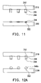
- first and second flip chips 110 , 130 are provided.
- the first flip chip 110 has a first chip 112 and a first bump 122 .
- the first chip has several first terminals 114 exposed at the surface of the first chip 112 .
- Each of the first bumps 122 is positioned on the corresponding first terminal 114 .
- the first bumps 122 are in ball patterns.
- the second flip chip 130 includes a second chip 132 and multiple second bumps 143 .
- the second flip chip 130 further has multiple second terminals 134 exposed at the surface of the second chip 132 .
- Each of the second bumps 142 is located on the corresponding second terminal 134 .
- the second bumps 142 have ball shape.
- the first chip and the second chip are then connected to each other.
- the first bumps 122 are dipped with flux 150 as shown in FIG. 2 .
- the first flip chip 110 is then turned up side down, such that each first bump 122 is aligned and pressed on one corresponding second bump 142 . Meanwhile, the joint between the first bump 122 and the second bump 142 is covered with the flux 150 as shown in FIG. 3 .
- both the first and second bumps 122 and 142 are in ball shape, a sliding motion between the first and second bumps 122 and 142 is inevitable when the first bumps 122 are pressed on the second bumps 142 . Therefore, a displacement or shift between the first and second bumps 122 and 142 is caused.
- a reflow process is then performed allowing each first bump 122 and the corresponding second bump 142 melted to form a common connecting block 160 , while the flux 150 flows to an external surface of the connecting block 160 to cover the connecting block 160 as shown in FIG. 4 .
- the neighboring blocks 160 may contact each other during the reflow process. A short circuit is thus caused to reduce the package yield.
- a solution (not shown) is applied to remove the residual flux 150 on the blocks 160 to form the structure as shown in FIG. 5 .
- the height of the connecting blocks 160 is limited, such that the distance between the first and second chip 112 and 132 is too small.
- the encapsulating material (not shown) can hardly flowing between the first and second chips 112 and 132 , such that void is formed therebetween, and the reliability of the package is degraded.
- the present invention provides a method of assembling chips with greatly enhanced assemble reliability.
- the present invention provides a method of assembling carriers between which the distance is increased.
- the preposition “on” means the relative geometric relationship between two objects being or being not in contact with each other. For example, when A is on B, A can be disposed on B with or without a direct contact in between.
- the method of assembling chips comprises the following steps.
- a first chip and a second chip are provided. At least a conductive pillar is formed on the first chip, and at least a conductive connecting material is formed on the conductive pillar.
- the conductive connecting material is connected to the second chip, such that the first chip and the second chip are electrically connected to each other via the conductive pillar and the conductive connecting material.
- the conductive connecting material is carried on the second chip or the conductive connecting material on the second chip with a surface contact.
- the sliding motion between the conductive connecting material on the conductive pillar and the second chip or on the conductive connecting material of the second chip can be suppressed.
- the first and second chips can thus be connected with accurate alignment, and the short circuit effect between the connecting members is avoided.
- the present invention provides a method of assembling carriers including the following steps.
- a first chip and a second chip are provided.
- At least a conductive pillar is formed on the first chip, and at least a conductive connecting material is formed on the second chip.
- the conductive pillar is connected to the conductive connecting material, such that the first carrier and the second carrier are electrically connected to each other via the conductive pillar and the conductive connecting material.
- the conductive pillar is pressed on the conductive connecting material on the second chip with a surface contact, and the sliding motion between the conductive pillar and the conductive connecting material on the second chip is effectively avoided.
- the first and second chips can be properly aligned and connected. The short circuit can thus be prevented.
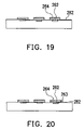
- the present invention further provides a method of fabricating a multi-chip package module.
- a first chip, a second chip and a carrier are provided.
- Multiple conductive pillars are formed on the first chip, and a conductive connecting material is formed on the conductive pillars.
- the conductive pillars are connected to the second chip via the conductive connecting material, such that the second chip is attached to and electrical connected to the first chip via the conductive pillars and the conductive connecting material.
- the first chip is then mounted to and electrically connected to the carrier.
- the present invention further provides a method of fabricating a multi-chip package module.
- a first chip, a second chip and a carrier are provided.
- Multiple conductive pillars are formed on the first chip, and a conductive connecting material is formed on the second chip.
- the conductive pillars are connected to the conductive connecting material, such that the second chip is attached to and electrical connected to the first chip via the conductive pillars and the conductive connecting material.
- the first chip is then mounted to and electrically connected to the carrier.
- a multi-chip package module in one embodiment, includes a first chip, a second chip, multiple conductive pillars and a carrier.
- the conductive pillars are located between the first and second chips, while the first chip is mounted to the carrier and electrically connected thereto.
- the carrier includes a substrate, a ceramic substrate, or a leadframe.
- An assembly structure is further provided in the present invention, including a first chip, a second chip and a conductive pillar located between the first and second chips.
- the melting point of the conductive pillar is configured higher than the connecting temperature of the conductive connecting material, such that the conductive pillar is not melted during the reflow process to maintain the space between the first and second chips. Therefore, a proper space between the first and second chips is sufficiently large, allowing the packaging material easily filled between the first and second chips in the following encapsulating process.
- a lead-free material can be used for forming the conductive pillar and the conductive connecting material to meet the environmental requirement.
- FIGS. 1 to 5 are cross sectional views showing the connecting process of flip chips.
- FIGS. 6 and 7 are cross sectional views showing the method of assembling carriers according to a first embodiment of the present invention.
- FIGS. 8A , 8 B and 9 are cross sectional views showing the method of assembling carriers according to a second embodiment of the present invention.
- FIG. 10 is a cross sectional views showing the method of assembling carriers according to a third embodiment of the present invention.
- FIG. 11 is a cross sectional views showing the method of assembling carriers according to a fourth embodiment of the present invention.
- FIGS. 12A and 12B are cross sectional views showing the method of assembling carriers according to a fifth embodiment of the present invention.
- FIGS. 13 and 14 are cross sectional views showing a method of assembling carriers in a sixth embodiment of the present invention.
- FIGS. 13A and 13B are laterally cross-sectional views showing conductive pillars 230 and 262 in a sixth embodiment of the present invention.
- FIGS. 15 to 21 are cross sectional views showing the process of forming the conductive pillar and the conductive connecting material on the second carrier as shown in the sixth embodiment.
- FIGS. 22 to 29 are cross sectional enlarged views showing a first example of fabricating a multi-chip package module according to the present invention.
- FIGS. 30 to 32 are cross sectional enlarged views showing a third example of fabricating a multi-chip package module according to the present invention.
- FIG. 33 to 36 are cross sectional enlarged views showing a third example of fabricating a multi-chip package module according to the present invention.
- FIGS. 37 to 42 are cross sectional enlarged views showing a fourth example of fabricating a multi-chip package module according to the present invention.
- FIG. 43 is a cross sectional enlarged view showing a fifth example of fabricating a multi-chip package module according to the present invention.
- FIGS. 44 and 45 show the method of assembling chips according to an embodiment of the present invention.
- FIGS. 44A , 44 B and 44 C show constructions of forming a conductive pillar and an under-bump-metallurgy layer over a bump pad.
- FIGS. 46 and 47 show the structure of assembling chips according to other embodiments of the present invention.
- FIG. 48 shows the method of assembling chips according to another embodiment of the present invention.
- FIGS. 6 and 7 a cross sectional schematic view of a method for assembling carriers according to the first embodiment of the present invention is shown.
- two carriers 210 , 220 that is, the first and second carriers 210 and 220 are provided.
- the first carrier 210 has multiple terminals 212 exposed at a surface thereof.
- the second carrier 220 has multiple terminals 222 exposed at a surface thereof.
- the first and second carrier 210 and 220 each includes a chip, a substrate or a ceramic substrate.
- Multiple conductive pillars 230 are formed on the terminals 212 of the first carrier 210 , while a conductive connecting material 240 is formed on each of the terminals 222 of the second carrier 220 .
- the material of the conductive pillars 230 is selected from tin, lead, copper, gold, silver, zinc, bismuth, magnesium, antimony, indium and an alloy thereof.
- the conductive connecting material 240 is in a paste form and can be formed by mixing metal particles and a flux.
- the conductive connecting material 240 can be formed on each terminal 222 of the second carrier 220 via screen printing.
- the metal particles include particles of tin, lead, copper, gold, silver, zinc, bismuth, magnesium, antimony, indium and an alloy thereof.
- the first carrier 210 is flipped with each conductive pillar 230 facing and aligned with the conductive connecting material 240 , such that each conductive pillar 230 is pressed on the conductive connecting material 240 .
- a reflow process is performed allowing the metal particles of the conductive connecting material 240 melted and cured into a connecting block 241 to connect the conductive pillars 230 with the terminals 222 of the second carrier 220 .
- the melting point of the conductive pillars 230 is higher than the fusion temperature of the conductive connecting material 240 .
- the connecting block is connected to only one side of the conductive pillars 230 .
- the flux of the conductive connecting material 230 flows to a surface of the connecting block 241 .
- a solution is used to remove the residual flux on the surface of the connecting block 241 to form the structure as shown in FIG. 7 .
- the conductive connecting materials 242 a and 242 b are in solid form such as pillar or ball (the conductive connecting material 242 a is in a ball form in FIG. 8A and the conductive connecting material 242 b is in a pillar form in FIG. 8B ).
- the material of the conductive connecting materials 242 a and 242 b includes tin, lead, copper, gold, silver, zinc, bismuth, magnesium, antimony, indium or an alloy of the above materials.
- the melting point of the conductive pillar 230 is higher than the fusion temperature of the conductive connecting materials 242 a and 242 b.
- the conductive connecting material 242 a are solder balls and the solder balls 242 a have a ball height a 1 greater than 15 micrometers.
- the conductive connecting material 242 b is solder bumps and the solder bumps 242 b have a bump height a 2 greater than 15 micrometers.
- the conductive pillars 230 are formed on the terminals 212 of the first carrier 210 and the conductive connecting materials 242 a and 242 b are formed on the terminals 222 of the second carrier 220 .
- the conductive connecting materials 242 a and 242 b are dipped with a flux (not shown).
- the first carrier 210 is flipped to press each of the conductive pillars 230 to the corresponding conductive connecting materials 242 a and 242 b.
- a reflow process is performed to melt the conductive connecting materials 242 a and 242 b for covering the conductive pillars 230 as shown in FIG. 9 .
- a solution is used to remove the flux remained on the conductive connecting materials 242 a and 242 b.
- FIG. 10 shows the method of assembling carriers according to a third embodiment of the present invention.
- the members denoted by the same numeral references in this and the first embodiments indicate the same devices, and an addition description is not further provided.
- the conductive connecting material 244 is formed on the conductive pillars 230 .
- the conductive connecting material 244 is in solid form such as pillar or ball.
- the material of the conductive connecting material 244 includes tin, lead, copper, gold, silver, zinc, bismuth, magnesium, antimony, indium or an alloy of the above materials.
- the melting point of the conductive pillar 230 is higher than the fusion temperature of the conductive connecting material 244 .
- the process of the conductive pillars 230 and the conductive connecting material 244 is incorporated by reference to Chinese Patent Application Nos. 90104979 and 91100092.
- the first carrier 244 is turned up side down.
- a reflow process is performed to connect the conductive connecting material 244 with the terminal 222 of the second carrier 220 .
- the first and second carriers 210 and 220 are electrically connected via the conductive pillars 230 and the conductive connecting material 244 .
- the paste-like conductive connecting material 230 can also be formed on the conductive pillar 230 by dipping adhesion.
- the paste-like conductive connecting material 230 includes a mixture of multiple metal particles and a flux.
- the metal particles include tin, lead, copper, gold, silver, zinc, bismuth, magnesium, antimony, indium or an alloy of the above metals.
- FIG. 11 shows the method of assembling carriers according to a fourth embodiment of the present invention.
- the members denoted by the same numeral references in this and the third embodiments indicate the same devices, and an addition description is not further provided.
- the conductive pillars 230 are formed on the terminals 212 of the first carrier 210 , and the conductive connecting material 244 is formed on the conductive pillars 230 .
- a conductive connecting material 246 is further formed on the terminals 222 of the second carrier 220 .
- the conductive connecting material 246 includes paste mixed with metal particles and a flux.
- the conductive connecting material 246 can be formed on the terminals 222 of the second carrier 220 by screen-printing.
- the metal particles of the conductive connecting material 246 include tin, lead, copper, gold, silver, zinc, bismuth, magnesium, indium or an alloy of these materials.
- the first carrier 210 is then flipped, allowing the conductive pillars 230 aligned with the corresponding conductive connecting material 246 .
- the conductive connecting material 244 on the conductive pillars 230 are then pressed on the conductive connecting material 246 .
- a reflow process is performed, such that the metal particles in the conductive connecting material 246 are merged and cured with the conductive connecting material 244 to form a connecting block (not shown), while the flux of the conductive connecting material 246 flows to a surface of the connecting block.
- the connecting block can be merged at one side of the conductive pillars 230 or to cover the conductive pillars 230 .
- a solution is used to remove the residual flux on the connecting block.
- the conductive pillars 230 can be connected to the terminals 222 of the second carrier 220 .
- the melting point of the conductive pillars 230 is higher than the fusion temperature of the conductive connecting materials 244 and 246 .
- FIGS. 12A and 12B are cross sectional views showing the method of assembling carriers according to a fifth embodiment of the present invention.
- the members denoted by the same numeral references in this and the third embodiments indicate the same devices, and an addition description is not further provided.
- the conductive connecting materials 248 a, 248 b can be in solid form with pattern such as ball or pillar (the conductive connecting material 248 a has a ball shape in FIG. 12A , and the conductive connecting material 248 b has a pillar shape, as shown in FIG. 12B ).
- the material of the conductive connecting materials 248 a and 248 b includes tin, lead, copper, gold, silver, zinc, bismuth, magnesium, antimony, indium, or an alloy thereof.
- the melting point of the conductive pillars 230 is higher than the adhesion temperature between the conductive connecting materials 248 a and 248 b.
- the conductive connecting material 244 is formed on the conductive pillars 230
- the conductive connecting materials 248 a and 248 b are formed on the terminals 222 of the second carrier 220
- the conductive connecting materials 248 a and 248 b are dipped with a flux.
- the first carrier 210 is flipped to press each conductive pillar 230 on the conductive connecting materials 248 a and 248 b.
- a reflow process is then performed to merge the conductive connecting materials 248 a, 248 b with the conductive connecting material 244 to form a connecting block (not shown).
- the connecting block can be formed at one side of the conductive pillars or to cover the conductive pillars.
- a solution is then used to remove the residual flux on the connecting block.
- the melting point of the conductive pillar is higher than the fusion temperature of the conductive connecting material, such that the conductive pillar will not be melted in the reflow process.
- a sufficient large distance between the first carrier and the second carrier can thus be maintained thereby. Therefore, in the subsequent encapsulating process, the encapsulating material is easily to fill between the first and second carriers.
- conductive pillars 230 are formed on each terminal 212 of the first carrier 210 .
- the material of the conductive pillar 230 includes tin, lead, copper, gold, silver, zinc, bismuth, magnesium, antimony, indium or an alloy of the above materials.
- Conductive pillars 262 and a conductive connecting material 264 are further formed on each terminal 222 of the second carrier 220 .
- the conductive pillars 262 are located on each terminal 222 , while the conductive connecting material 264 is formed on the conductive pillars 262 and has a bottom surface 266 in contact with the conductive pillars 262 .
- the materials of the conductive pillars 262 and the conductive connecting material 264 includes tin, lead, copper, gold, silver, zinc, bismuth, magnesium, antimony, indium or an alloy of the above materials. Further, the melting points of the conductive pillars 230 and 262 are higher than the temperature, and the conductive connecting material 264 extends beyond the conductive connecting material 264 with the bottom surface thereof exposed.
- the cross section of the conductive pillars 262 is substantially the same as that of the conductive pillars 230 .
- the minimum distance d between the edge of the conductive connecting material 264 and the edge of the conductive pillars 262 is no shorter than about 5 microns.
- the height of the conductive pillars 230 is higher than that of the conductive pillars 262 and the height a 3 of the conductive pillar 262 is smaller than 25 micrometers.
- the conductive pillars 230 and 262 have a cross section with the same shape and dimension.
- the conductive pillars 230 and 262 have a cross section with the substantially similar shape and substantially close dimension.
- the conductive pillars 230 and 262 have a laterally cross-section with square shaped, for example, and the substantially close dimensions w 1 and w 2 are within 10 micrometers per side, as shown in FIGS. 13A and 13B .
- the conductive pillars 230 and 262 have a laterally cross-section with circular shaped.
- the conductive connecting material 264 is dipped with a flux and flipped to align each conductive pillar 230 with the conductive connecting material 264 .
- the conductive pillars 230 are thus pressed on the conductive connecting material 264 , and a reflow process is performed.
- the conductive connecting material 240 is thus in a fusion state to cover the conductive pillars 230 and 262 in a manner as shown in FIG. 14 .
- a solution is then used to remove the flux remaining on the conductive connecting material 264 .
- the fabrication method of the conductive pillars 262 and the conductive connecting material 264 is introduced as follows.
- FIGS. 15 to 21 the sixth embodiment for forming the conductive pillars and the conductive connecting material on the second carrier is illustrated.
- a second carrier 220 is provided, and a glue layer 282 is formed on the second carrier 220 by sputtering or evaporation.
- the material of the glue layer 282 includes titanium, titanium-tungsten alloy, titanium-nitrogen alloy or chromium.
- a photoresist layer 290 is formed on the glue layer 282 by adhesion or spin-coating. The exposure, development are then performed to transfer a pattern to the photoresist layer 290 , which then comprises a plurality of openings 292 exposing the glue layer 282 over the terminals 222 of the second carrier 220 as shown in FIG. 16 . Using electroplating, a conductive pillar 262 is formed in each opening 292 of the photoresist layer 290 and located on the glue layer 220 exposed thereby to form the pattern as shown in FIG. 17 .
- the material for forming the conductive pillars 262 includes tin, lead, copper, gold, silver, zinc, bismuth, magnesium, antimony, indium or an alloy of the above materials.
- the conductive connecting material 264 is formed in the openings 292 of the photoresist layer 290 and located on the conductive pillars 262 as shown in FIG. 18 .
- the material for forming the conductive connecting material 264 includes tin, lead, copper, gold, silver, zinc, bismuth, magnesium, antimony, indium or an alloy of the above materials.
- the melting point of the conductive pillars 262 is higher than the connecting temperature of the conductive connecting material 264 .
- the photoresist layer 290 is then removed to expose the glue layer 282 as shown in FIG. 19 .
- a wet etching process is then performed using the conductive pillars 262 and the conductive connecting material 264 as mask to remove the exposed glue layer 282 to form the structure as shown in FIG. 20 .
- a wet etching process is further performed with the conductive connecting material 264 as a mask, so that the sidewall of the conductive pillars 262 are etched to result in reduction in cross section thereof. Consequently, the bottom surface 266 of the conductive connecting material 264 is exposed as shown in FIG. 21 .
- the shortest distance between the edge of the conductive connecting material 264 and the edge of the conductive pillars 262 is no smaller than 5 microns.
- the conductive pillars will not be fused during the reflow process to properly support the distance between the first and second carriers. Therefore, a sufficiently large space between the first and second carriers can be maintained, allowing the packaging material filled between the first and second carriers easily in the following encapsulating process.
- the conductive pillar is supported on the conductive connecting material of the second carrier with a surface contact, such that the sliding motion between the conductive pillar and the conductive connecting material of the second carrier can be suppressed.
- the first and second carriers can be connected with precise alignment to avoid the short circuit of the connecting structures.
- the conductive connecting material formed on the conductive pillar can be supported on the conductive connecting material formed on the second carrier with a surface contact. Therefore, the sliding motion between the conductive connecting material on the conductive pillars and the conductive connecting material on the second carrier is suppressed, so that the first and second carriers can be connected with a precise alignment to avoid short circuit.
- the conductive pillars and the conductive connecting material can be formed of unleaded material for environmental concern.
- FIGS. 13 to 20 show a cross sectional enlarged schematic drawing of a method for fabricating a multi-chip package module.
- the method described in any of the previous embodiments can be applied to connect chips and connecting the chip and substrate in this embodiment. In the following description, only one method is illustrated.
- the connecting structure between chips and between chip and substrate is similar to the connecting structure between carriers as discussed in the previous embodiment. Only one kind of structure is illustrated in the following figures.
- the fabrication method of multi-chip package structure by applying the above connecting method between carriers is further described as follows. Referring to FIGS. 22 to 29 , a first embodiment for fabricating a multi-chip module is illustrated. The method for connecting chip and substrate as mentioned above can be applied in this embodiment. In the following description, the method for connecting the carriers is not repeated.
- a first chip 310 and a second chip 320 are provided.
- the first chip 210 has multiple terminals 312 exposed at an active surface 314 of the first chip 310 .
- the second chip has multiple terminals 322 exposed at an active surface 324 thereof.
- the first chip 310 includes digital logic chip, while the second chip 320 includes memory chip.
- Multiple conductive pillars 330 are formed on the terminals 312 of the first chip 310 .
- a conductive connecting material 340 is formed on the terminals 322 of the second chip 320 .
- the melting point of the conductive pillars 330 is higher than the fusion temperature of the conductive connecting material 340 .
- a merging process between the chips is then performed.
- the merging process includes a reflow process, for example.
- the conductive connecting material 340 is merged with the conductive pillars 330 on the central portion of the first chip 310 ; thereby, the second chip 320 is fixed to the central portion of the first chip 310 .
- the first and second chips 310 and 320 are thus electrically connected via the conductive pillars 330 and the conductive connecting material 340 as shown in FIG. 14 .
- a carrier 350 such as an organic, glass, ceramic or metal substrate is provided.
- the carrier 350 includes a surface 352 and a rear surface 354 opposing to the surface 352 .
- the carrier 350 has a plurality of terminals 356 and 358 exposed at the surfaces 352 and 354 , respectively.
- the carrier 350 further includes an opening 359 perforating through the center thereof.
- a conductive connecting material 360 is formed on the terminals 356 of the carrier 350 .
- the melting point of the conductive pillars 330 is higher than the fusion temperature of the conductive connecting material 360 .
- the connecting process between the chip and the substrate is then performed. For example, a reflow process is performed to merge the conductive connecting material 360 and the conductive pillars 330 located at a periphery of the first chip 310 , such that the first chip can be mounted to the carrier 350 . Meanwhile, the second chip 320 is accommodated in the opening 359 . Via the conductive pillars 330 formed at the periphery of the first chip 310 and the conductive connecting material 360 , the first chip 310 is electrically connected to the carrier 350 as shown in FIG. 25 .
- a film 370 can be adhered to the rear surface 354 to seal the opening 359 of the carrier 350 at the rear surface 354 as shown in FIG. 26 .
- a first encapsulating material 380 is filled in the opening 359 of the carrier 350 , and spaces between the first chip 310 and second chip 320 and between the first chip 310 and the carrier 350 .
- the encapsulating material 380 covers the second chip 320 as shown in FIG. 27 .
- the film 370 is then removed from the rear surface 354 of the carrier 350 to form the structure as shown in FIG. 28 .
- a plurality of solder balls 390 are formed on the terminals 358 on the rear surface 354 of the carrier 350 as shown in FIG. 29 .
- the multi-chip package module 300 is thus formed.
- the connection between the multi-chip package module 300 and an external circuit is established via the solder balls 390 .
- the encapsulating material is filled in the opening, the spaces between the first and second chips, and between the first chip and the carrier using glue dispensing.
- the present invention is not limited to the method only. Other methods, such as those illustrated in FIGS. 30 to 32 which illustrate a second embodiment of multi-chip package module, can also be applied.
- the film 370 is adhered to the rear surface 354 of the carrier 350 .
- the first encapsulating material 382 is filled in the opening 359 of the carrier 350 , the space between the chips 310 and 320 , and the space between the first chip 310 and the carrier 350 using glue injection. Thereby, the first chip 310 and the second chip 320 are covered with the encapsulating material 380 .
- the film 370 is then removed from the rear surface 354 of the carrier 350 to form the structure as shown in FIG. 31 .
- a plurality of solder balls 390 are then formed on the terminals 358 on the rear surface 354 of the carrier 350 via ball planting to form the structure as shown in FIG. 32 .
- the multi-chip package module 302 is formed and the electric connection between the multi-chip package module 302 and an external circuit is established via the solder balls 390 .
- the first chip is connected to the carrier after the first chip and the second chip are connected to each other. It is appreciated that the present invention is not limited to such sequence only. The sequence of connecting the first chip and the second chip after mounting the first chip to the carrier can also be applied in the present invention.
- FIGS. 33 to 36 show a third embodiment of fabricating multi-chip package module according to such sequence.
- the devices denoted by the same numeral references as the first embodiment indicate the same or similar devices.
- a first chip 310 and a carrier 350 are provided.
- Multiple conductive pillars 330 are formed on the terminals 312 of the first chip 310 , and a conductive connecting material 332 is formed on the conductive pillars 330 .
- the methods of fabricating the conductive pillars 330 and the conductive connecting material 332 are incorporated by reference to the Chinese Patent Application Nos. 90104979 and 91100092.
- the melting point of the conductive pillars 330 is higher than the fusion temperature of the conductive connecting material 332 .
- the connecting process of the chip and the substrate is performed. For example, a reflow process is performed to connect the conductive connecting material 332 at a periphery of the first chip 310 with the terminals 356 of the carrier 350 . Thereby, the first chip 310 is mounted and electrically connected to the carrier 350 via the conductive pillars 330 and the conductive connecting material 332 as shown in FIG. 34 .
- a second chip 320 is provided, and a conductive connecting material 342 is formed on the terminals 322 of the second chip 320 .
- the melting point of the conductive pillars 330 is higher than the fusion temperature of the conductive connecting material 342 .
- the chip connecting process is then performed. For example, a reflow process is performed to merge the conductive connecting material 342 on the terminal 322 of the second chip 320 and the conductive connecting material 332 on the conductive pillars 330 formed on the central portion of the first chip 310 to form a connecting block 344 which covers the conductive pillars 330 on the central portion of the first chip 310 . As shown in FIG.
- the second chip 320 is mounted on a central portion of the first chip 310 .
- the first chip 310 and the second chip 320 are electrically connected via the conductive pillars 330 and the connecting block 344 .
- the glue dispensing or injection step is then performed as illustrated in the first and second embodiments.
- the conductive pillar and the conductive connecting material are used to electrically connect the first chip and the carrier.
- the present invention is not limited to such electric connection.
- Other method such as wire bonding can also be used for electrically connecting the first chip and the carrier as shown in FIGS. 37 to 42 , which illustrate the cross sectional view of the multi-chip package module fabrication in a fourth embodiment of the present invention.
- a first chip 410 and a second chip 420 are provided.
- the first chip 410 has an active surface 414 and a rear surface 416 opposing to the active surface 414 .
- the first chip 410 has a plurality of terminals 412 formed on the active surface 414 .
- a plurality of conductive pillars 430 is formed on the terminals 412 of the active surface 414 of the first chip 410 .
- a conductive connecting material 432 is formed on the conductive pillars 430 .
- the method for forming the conductive pillars 430 and the conductive connecting material 432 is incorporated by reference to the Chinese Patent Application Nos. 90104979 and 91100092.
- the melting point of the conductive pillars 430 is higher than the fusion temperature of the conductive connecting material 432 .
- the connecting process between the chips is performed. For example, a reflow process is performed to connect the terminals 422 of the second chip 420 to the conductive connecting material 432 on the conductive pillars 430 on the central portion of the first chip 410 .
- the second chip 420 can thus be mounted to the central portion of the first chip 410 .
- the first chip 410 can thus be electrically connected to the second chip 420 via the conductive pillars 430 and the conductive connecting material 432 as shown in FIG. 38 .
- a carrier 450 such as a substrate or a ceramic substrate is provided.
- the carrier 450 has a surface 452 and a rear surface 454 opposing to the surface 452 .
- the carrier 450 has a chip frame 459 , multiple terminals 456 and 458 .
- the chip frame 459 and the terminals 456 are exposed at the surface 452 , while the terminals 458 are exposed at the rear surface 454 .
- the terminals 456 are formed in two rows at a periphery of the chip frame 459 , while the terminals 458 are formed in an array on the rear surface 454 .
- An adhesive material 460 is then used to adhere the rear surface 416 of the first chip 410 to the chip frame 459 of the carrier 450 .
- the first chip 410 and the carrier 450 are electrically connected via wire bonding.
- the wire 470 has one end connected to one of the terminals 412 at the periphery of the active surface 414 of the first chip 410 , and the other end connected to one of the terminals 456 as shown in FIG. 40 .
- An encapsulating material 480 is formed by injection to cover the first chip 410 , the second chip 420 , the wire 470 and the surface 452 of the carrier 450 .
- the encapsulating material 480 fills the space between the first chip 410 and the second chip 420 as shown in FIG. 41 .
- a plurality of solder balls 490 is then formed using ball planting on the terminals 458 of the rear surface 454 of the carrier 450 as shown in FIG. 42 .
- the multi-chip package module is thus fabricated.
- the electric connection between the multi-chip package module and an external circuit (not shown) is established via the solder balls 390 .
- the carrier includes a substrate or a ceramic substrate.
- the carrier also includes a leadframe as shown in FIG. 43 , which illustrates the multi-chip package module in a fifth embodiment of the present invention.
- the carrier 550 includes a chip frame 552 and multiple leads 554 surrounding the chip frame 552 .
- the first chip 510 and the second chip 520 are connected before connecting to the carrier.
- An adhesive 560 is used to adhere the rear surface 516 of the first chip 510 to the chip frame 552 of the carrier 550 .
- the first chip 510 is then electrically connected to the leads 554 of the leadframe 550 via wire bonding.
- the wires 570 have one ends connected to the terminals 512 at the periphery of the active surface 514 of the first chip, and the other ends connected to one ends of the leads 554 .
- a encapsulating material 580 is formed by injection to cover the first chip 510 , the second chip 520 , the wires 570 , the chip frame 552 of the carrier 550 , and the ends of the leads 554 near the chip frame 552 .
- the encapsulating material 580 also fills the space between the first chip 510 and the second chip 520 .
- a trimming and forming process is then performed to cut the dam bar exposed between the leads 554 of the encapsulating material 580 .
- the exposed portions of the leads 554 are then bent into the gull wing type as shown in FIG. 34 .
- the electrical connection between the multi-chip package module and an external circuit is thus established via the leads 554 of the carrier 550 .
- FIGS. 44 and 45 showing the method of assembling chips according to an embodiment of the present invention, there are two chips 610 , 710 bonded using a flip-chip technology.
- the chip 610 is provided with bumps 620 shaped like balls.
- the chip 610 has multiple metal contacts 630 formed on an active surface 612 of the chip 610 .
- An under-bump-metallurgy (UBM) layer 640 is formed on the metal contacts 630 .
- the under-bump-metallurgy layer 640 can be a single-layer structure or a multi-layer structure made of one or several of the materials selected from copper, nickel and gold.
- the under-bump-metallurgy layer 640 can be constructed, stacking from the bonding pads, from a titanium layer and a copper layer, or a titanium layer, a copper layer and a nickel layer, or a titanium layer, a copper layer, a nickel layer and a gold layer, or a titanium-tungsten-alloy layer and a gold layer, or a chromium layer, a copper layer and a nickel layer.
- the bumps 620 are formed on the under-bump-metallurgy layer 640 .
- the bumps 620 have a height h larger than 15 microns, for example.
- the material constituting the bumps 620 comprises a tin-lead alloy, a tin-silver alloy, a tin-silver-copper alloy, a tin-bismuth alloy, a tin-silver-indium alloy, a tin-bismuth-zinc alloy, a tin-zinc alloy, a tin-bismuth-silver-copper alloy, a tin-silver-copper-antimony alloy, a tin-antimony alloy or a tin-zinc-indium-silver alloy.
- the chip 710 has multiple electronic devices 712 , such as transistors or MOS devices, formed on a surface of a semiconductor substrate 711 , wherein the semiconductor substrate 711 is, for example, silicon.
- Multiple dielectric layers 722 , 724 , and 726 are stacked on the semiconductor substrate 711 and have a plurality of via holes 728 (only shown one of them).
- Multiple fine-line interconnection layers 732 , 734 , and 736 are disposed on the dielectric layers 722 , 724 , and 726 , respectively, and the circuit layer 736 has multiple original pads 738 .
- the fine-line interconnection layers 732 , 734 , and 736 are electrically connected with each other through the via holes 728 and are electrically connected to the electronic devices 712 .
- the fine-line interconnection layers 732 , 734 , and 736 are formed, for example, by depositing aluminum or an aluminum alloy using a PVD process or by depositing copper or a copper alloy using electroplating processes and dama
- a passivation layer 740 is formed over the dielectric layers 722 , 724 , and 726 and over the circuit layers 732 , 734 and 736 .
- the passivation layer 740 has a thickness t, for example, larger than 0.35 micrometers. It should be noted that the passivation layer 740 should have enough thickness to prevent moisture, impurities, mobile ions or transitional metal elements from penetrating therethrough.
- the passivation layer 740 can be a silicon-dioxide layer, a silicon-nitride layer, a phosphosilicate glass (PSG) layer, a silicon-oxynitride layer or a composite structure comprising the above-mentioned layers.
- the passivation layer 740 has openings 742 exposing the original pads 738 .
- the openings 742 have a width larger than about 0.1 micrometers, for example.
- the chip 710 further comprises a post-passivation metal scheme 750 formed over the passivation layer 740 .
- the post-passivation metal scheme 750 comprises a gold layer 752 and an adhesion/barrier layer 754 , wherein the gold layer 752 is positioned over the adhesion/barrier layer 754 .
- the gold layer 752 has a thickness g larger than 1 micron and can be formed by electroplating.
- the adhesion/barrier layer 754 comprises a titanium-tungsten alloy, titanium, titanium-nitride or tantalum-nitride.
- the post-passivation metal scheme 750 comprises redistribution transition lines 751 , a plurality of bump pads 753 and a plurality of wire-bonding pads 755 , and the redistribution transition lines 751 connects the bump pads 753 or the wire-bonding pads 755 to the original pads 738 .
- UBM under-bump-metallurgy
- the material constituting the connecting pads 760 comprises a high lead solder, a tin-lead alloy, a tin-silver alloy, a tin-silver-copper alloy, a tin-bismuth alloy, a tin-silver-indium alloy, a tin-bismuth-zinc alloy, a tin-zinc alloy, a tin-bismuth-silver-copper alloy, a tin-silver-copper-antimony alloy, a tin-antimony alloy or a tin-zinc-indium-silver alloy.
- the under-bump-metallurgy layer 770 can be a multi-layer structure, as shown in FIGS. 44A , 44 B and 44 C.
- the under-bump-metallurgy layer 770 comprises a titanium layer 772 a, a copper layer 772 b and a nickel layer 772 c.
- the titanium layer 772 a is positioned on the bump pads 753 ;
- the copper layer 772 b is positioned on the titanium layer 772 a;
- the nickel layer 772 c is positioned on the copper layer 772 b;
- the connecting pads 760 are formed on the nickel layer 772 c.
- the under-bump-metallurgy layer 770 comprises a titanium-tungsten-alloy layer 774 a, a copper layer 774 b and a nickel layer 774 c.
- the titanium-tungsten-alloy layer 774 a is positioned on the bump pads 753 ;
- the copper layer 774 b is positioned on the titanium-tungsten-alloy layer 774 a;
- the nickel layer 774 c is positioned on the copper layer 774 b;
- the connecting pads 760 are formed on the nickel layer 774 c.
- the under-bump-metallurgy layer 770 comprises a chromium layer 776 a, a copper layer 776 b and a nickel layer 776 c.
- the chromium layer 776 a is positioned on the bump pads 753 ; the copper layer 776 b is positioned on the chromium layer 776 a; the nickel layer 776 c is positioned on the copper layer 776 b; the connecting pads 760 are formed on the nickel layer 776 c.
- a reflow process can be performed to joint the bumps 620 with the connecting pads 760 , as shown in FIG. 45 .
- an underfill 780 is filled between the chips 610 and 710 and covers the bumps 620 .
- a wire-bonding process can be performed to form multiple wires 790 connecting the wire-bonding pads 755 to an external circuit, such as circuit substrate.
- FIG. 46 shows the method of assembling chips according to another embodiment of the present invention.
- Polymer layers 810 and 820 are made of, for example, polyimide, benzocyclobutene, porous dielectric material, parylene, or elastomer.
- the polymer layer 810 is formed between the circuit layer 750 and the passivation layer 740 and has a plurality of via-holes 812 , through which the circuit layer 750 is connected to the original pads 738 .
- the polymer layer 820 is formed on the circuit layer 750 and has a plurality of openings 822 and 824 exposing the bump pads 753 and the wire-bonding pads 755 , respectively.
- FIG. 47 shows the method of assembling chips according to another embodiment of the present invention.
- a polymer layer 810 a is formed between the circuit layer 750 a and the passivation layer 740 .
- Polymer layers 810 b and 810 c are formed between the circuit layers 750 a, 750 b, 750 c.
- a polymer layer 810 d is formed on the circuit layer 750 c.
- the polymer layer 810 a, 810 b, 810 c, 810 d are made of polyimide, benzocyclobutene, porous dielectric material, parylene, or elastomer.
- FIG. 48 shows the method of assembling chips according to another embodiment of the present invention.
- Bumps 620 are formed on the chip 710 , while connecting pads 760 are formed on the chip 610 .
- An under-bump-metallurgy layer 640 can be formed between the gold layer 752 and the bumps 620 .
- An under-bump-metallurgy layer 770 can be formed between the metal contacts 630 and the connecting pads 760 .
- the material and the construction of the bumps 620 , connecting pads 760 and under-bump-metallurgy layers 640 and 770 can be referred to the elements with the same reference number in the above description.
- the bumps 620 have a height h larger than 15 microns, for example.
- the present invention has the following advantages.
- the melting point of the conductive pillars is higher than the fusion temperature of the conductive connecting material, such that the conductive pillar will not be melted during the reflow process.
- the distance between the first and second chips can thus be maintained thereby, allowing the encapsulating material to fill the space between the first and second chips in the subsequent process.
- the conductive pillars are supported by the conductive connecting material on the second chip with surface contact, so that the sliding motion between the conductive pillars and the conductive connecting material on the second chip is suppressed.
- the first and second chips can thus be connected with precise alignment to avoid short circuit.
- the conductive connecting material on the conductive pillars is supported by the second chip or by the conductive connecting material on the second chip with a surface contact, so that the sliding motion is suppressed.
- the first and second chips can thus be connected with precise alignment to avoid short circuit.
- Unleaded material can be used for forming the conductive pillars and the conductive connecting material for environmental concern.
Abstract
Description
Claims (20)
Priority Applications (2)
| Application Number | Priority Date | Filing Date | Title |
|---|---|---|---|
| US12/128,644 US8021921B2 (en) | 2002-10-25 | 2008-05-29 | Method of joining chips utilizing copper pillar |
| US13/207,350 US8421222B2 (en) | 2002-10-25 | 2011-08-10 | Chip package having a chip combined with a substrate via a copper pillar |
Applications Claiming Priority (7)
| Application Number | Priority Date | Filing Date | Title |
|---|---|---|---|
| TW091125126A TWI313507B (en) | 2002-10-25 | 2002-10-25 | Method for assembling chips |
| TW91125126A | 2002-10-25 | ||
| TW91125126 | 2002-10-25 | ||
| US10/695,630 US7242099B2 (en) | 2001-03-05 | 2003-10-27 | Chip package with multiple chips connected by bumps |
| US11/123,328 US7382005B2 (en) | 2001-03-05 | 2005-05-06 | Circuit component with bump formed over chip |
| US12/109,367 US20080241992A1 (en) | 2001-03-05 | 2008-04-25 | Method of assembling chips |
| US12/128,644 US8021921B2 (en) | 2002-10-25 | 2008-05-29 | Method of joining chips utilizing copper pillar |
Related Parent Applications (2)
| Application Number | Title | Priority Date | Filing Date |
|---|---|---|---|
| US12/109,376 Continuation US8090302B2 (en) | 2007-11-16 | 2008-04-25 | Closing member for a developer containing device and method for producing such device |
| US12/109,367 Continuation US20080241992A1 (en) | 2001-03-05 | 2008-04-25 | Method of assembling chips |
Related Child Applications (1)
| Application Number | Title | Priority Date | Filing Date |
|---|---|---|---|
| US13/207,350 Continuation US8421222B2 (en) | 2002-10-25 | 2011-08-10 | Chip package having a chip combined with a substrate via a copper pillar |
Publications (2)
| Publication Number | Publication Date |
|---|---|
| US20080227237A1 US20080227237A1 (en) | 2008-09-18 |
| US8021921B2 true US8021921B2 (en) | 2011-09-20 |
Family
ID=39732496
Family Applications (5)
| Application Number | Title | Priority Date | Filing Date |
|---|---|---|---|
| US11/123,328 Expired - Lifetime US7382005B2 (en) | 2001-03-05 | 2005-05-06 | Circuit component with bump formed over chip |
| US12/109,367 Abandoned US20080241992A1 (en) | 2001-03-05 | 2008-04-25 | Method of assembling chips |
| US12/121,778 Abandoned US20080211105A1 (en) | 2002-10-25 | 2008-05-15 | Method of assembling chips |
| US12/128,644 Expired - Fee Related US8021921B2 (en) | 2002-10-25 | 2008-05-29 | Method of joining chips utilizing copper pillar |
| US13/207,350 Expired - Lifetime US8421222B2 (en) | 2002-10-25 | 2011-08-10 | Chip package having a chip combined with a substrate via a copper pillar |
Family Applications Before (3)
| Application Number | Title | Priority Date | Filing Date |
|---|---|---|---|
| US11/123,328 Expired - Lifetime US7382005B2 (en) | 2001-03-05 | 2005-05-06 | Circuit component with bump formed over chip |
| US12/109,367 Abandoned US20080241992A1 (en) | 2001-03-05 | 2008-04-25 | Method of assembling chips |
| US12/121,778 Abandoned US20080211105A1 (en) | 2002-10-25 | 2008-05-15 | Method of assembling chips |
Family Applications After (1)
| Application Number | Title | Priority Date | Filing Date |
|---|---|---|---|
| US13/207,350 Expired - Lifetime US8421222B2 (en) | 2002-10-25 | 2011-08-10 | Chip package having a chip combined with a substrate via a copper pillar |
Country Status (2)
| Country | Link |
|---|---|
| US (5) | US7382005B2 (en) |
| TW (1) | TWI313507B (en) |
Cited By (17)
| Publication number | Priority date | Publication date | Assignee | Title |
|---|---|---|---|---|
| US20100246150A1 (en) * | 2007-11-06 | 2010-09-30 | Agency For Science Tecnology And Research | Interconnect Structure And A Method Of Fabricating The Same |
| US20110067908A1 (en) * | 2008-05-21 | 2011-03-24 | Weichslberger Guenther | Method for producing a printed circuit board and use and printed circuit board |
| US20110215467A1 (en) * | 2010-03-04 | 2011-09-08 | Hung-Hsin Hsu | Metal post chip connecting device and method free to use soldering material |
| US20130068514A1 (en) * | 2011-09-21 | 2013-03-21 | Shou-Chian Hsu | Flip-chip carrier and fabricating method of mps-c2 package utilized from the same |
| US8421222B2 (en) | 2002-10-25 | 2013-04-16 | Megica Corporation | Chip package having a chip combined with a substrate via a copper pillar |
| US20140061897A1 (en) * | 2012-08-31 | 2014-03-06 | Taiwan Semiconductor Manufacturing Company, Ltd. | Bump Structures for Semiconductor Package |
| US8916448B2 (en) | 2013-01-09 | 2014-12-23 | International Business Machines Corporation | Metal to metal bonding for stacked (3D) integrated circuits |
| US8957524B2 (en) | 2013-03-15 | 2015-02-17 | Globalfoundries Inc. | Pillar structure for use in packaging integrated circuit products and methods of making such a pillar structure |
| US20150179622A1 (en) * | 2013-12-19 | 2015-06-25 | Omkar Karhade | Solder pad device and method |
| US20190096845A1 (en) * | 2017-05-09 | 2019-03-28 | Unimicron Technology Corp. | Chip module and stacked structure |
| US10559948B2 (en) * | 2018-05-08 | 2020-02-11 | Yazaki Corporation | Casing, electrical connection box, and wire harness |
| US10685922B2 (en) | 2017-05-09 | 2020-06-16 | Unimicron Technology Corp. | Package structure with structure reinforcing element and manufacturing method thereof |
| US20200203254A1 (en) * | 2018-12-21 | 2020-06-25 | Intel Corporation | Liquid thermal interface material in electronic packaging |
| US10950535B2 (en) | 2017-05-09 | 2021-03-16 | Unimicron Technology Corp. | Package structure and method of manufacturing the same |
| US11013103B2 (en) | 2017-05-09 | 2021-05-18 | Unimicron Technology Corp. | Method for forming circuit board stacked structure |
| US11508691B2 (en) | 2021-02-22 | 2022-11-22 | United Microelectronics Corp. | Semiconductor structure with nano-twinned metal coating layer and fabrication method thereof |
| US11749616B2 (en) | 2017-10-05 | 2023-09-05 | Texas Instruments Incorporated | Industrial chip scale package for microelectronic device |
Families Citing this family (59)
| Publication number | Priority date | Publication date | Assignee | Title |
|---|---|---|---|---|
| US8641913B2 (en) | 2003-10-06 | 2014-02-04 | Tessera, Inc. | Fine pitch microcontacts and method for forming thereof |
| US7214605B2 (en) * | 2003-10-09 | 2007-05-08 | Intel Corporation | Deposition of diffusion barrier |
| US7394161B2 (en) | 2003-12-08 | 2008-07-01 | Megica Corporation | Chip structure with pads having bumps or wirebonded wires formed thereover or used to be tested thereto |
| US7709968B2 (en) | 2003-12-30 | 2010-05-04 | Tessera, Inc. | Micro pin grid array with pin motion isolation |
| US20060019468A1 (en) | 2004-07-21 | 2006-01-26 | Beatty John J | Method of manufacturing a plurality of electronic assemblies |
| US8294279B2 (en) | 2005-01-25 | 2012-10-23 | Megica Corporation | Chip package with dam bar restricting flow of underfill |
| TWI251861B (en) * | 2005-06-16 | 2006-03-21 | Etron Technology Inc | Re-entrant Routing method and circuit structure |
| DE102005033469B4 (en) * | 2005-07-18 | 2019-05-09 | Infineon Technologies Ag | Method for producing a semiconductor module |
| TWI296839B (en) * | 2006-03-15 | 2008-05-11 | Advanced Semiconductor Eng | A package structure with enhancing layer and manufaturing the same |
| KR100893939B1 (en) * | 2007-02-16 | 2009-04-21 | 삼성전자주식회사 | Electronic device having a bonding pad structure and method of fabrication thereof |
| GB2463806B (en) * | 2007-05-08 | 2012-07-18 | Scanimetrics Inc | Ultra high speed signal transmission/reception |
| WO2009031586A1 (en) * | 2007-09-06 | 2009-03-12 | Murata Manufacturing Co., Ltd. | Circuit board and method for manufacturing circuit board |
| US20090065931A1 (en) * | 2007-09-11 | 2009-03-12 | Intel Corporation | Packaged integrated circuit and method of forming thereof |
| US8558379B2 (en) | 2007-09-28 | 2013-10-15 | Tessera, Inc. | Flip chip interconnection with double post |
| US8247267B2 (en) * | 2008-03-11 | 2012-08-21 | Taiwan Semiconductor Manufacturing Company, Ltd. | Wafer level IC assembly method |
| DE102008050840A1 (en) * | 2008-10-08 | 2009-10-15 | Siemens Aktiengesellschaft | Electrical module i.e. detector module, manufacturing method for X-ray measuring system of computer tomography scanner, involves soldering evaluation electronics of component with carrier substrate by low-temperature-guide |
| DE102008050838A1 (en) * | 2008-10-08 | 2009-10-15 | Siemens Aktiengesellschaft | Electric component for roentgen measuring system, has two semiconductor elements and contact element, where one semiconductor element is soldered on another semiconductor element, and contact element acts as tolerance compensation |
| US9024431B2 (en) | 2009-10-29 | 2015-05-05 | Taiwan Semiconductor Manufacturing Company, Ltd. | Semiconductor die contact structure and method |
| US20110186989A1 (en) | 2010-02-04 | 2011-08-04 | Taiwan Semiconductor Manufacturing Company, Ltd. | Semiconductor Device and Bump Formation Process |
| CN102237329B (en) * | 2010-04-27 | 2013-08-21 | 瑞鼎科技股份有限公司 | Chip structure, chip bonding structure and manufacturing methods for chip structure and chip bonding structure |
| KR20110124993A (en) * | 2010-05-12 | 2011-11-18 | 삼성전자주식회사 | Semiconductor chip and semiconductor package including the same and method of manufacturing the same |
| US8466543B2 (en) | 2010-05-27 | 2013-06-18 | International Business Machines Corporation | Three dimensional stacked package structure |
| US8330272B2 (en) | 2010-07-08 | 2012-12-11 | Tessera, Inc. | Microelectronic packages with dual or multiple-etched flip-chip connectors |
| US8580607B2 (en) * | 2010-07-27 | 2013-11-12 | Tessera, Inc. | Microelectronic packages with nanoparticle joining |
| US8293636B2 (en) * | 2010-08-24 | 2012-10-23 | GlobalFoundries, Inc. | Conductive connection structure with stress reduction arrangement for a semiconductor device, and related fabrication method |
| US8946890B2 (en) * | 2010-10-20 | 2015-02-03 | Marvell World Trade Ltd. | Power/ground layout for chips |
| US8853558B2 (en) | 2010-12-10 | 2014-10-07 | Tessera, Inc. | Interconnect structure |
| US9142520B2 (en) * | 2011-08-30 | 2015-09-22 | Ati Technologies Ulc | Methods of fabricating semiconductor chip solder structures |
| US9245834B2 (en) * | 2012-03-16 | 2016-01-26 | Stats Chippac, Ltd. | Semiconductor device and method of forming compliant conductive interconnect structure in flipchip package |
| US9087830B2 (en) * | 2012-03-22 | 2015-07-21 | Nvidia Corporation | System, method, and computer program product for affixing a post to a substrate pad |
| CN102543783B (en) * | 2012-03-28 | 2015-06-24 | 上海交通大学 | Hot compression chip low-temperature interconnection method using indium and micro needle cone structures |
| US9190348B2 (en) | 2012-05-30 | 2015-11-17 | Taiwan Semiconductor Manufacturing Company, Ltd. | Scheme for connector site spacing and resulting structures |
| US9691745B2 (en) | 2013-06-26 | 2017-06-27 | Taiwan Semiconductor Manufacturing Co., Ltd. | Bonding structure for forming a package on package (PoP) structure and method for forming the same |
| US9559071B2 (en) * | 2013-06-26 | 2017-01-31 | Taiwan Semiconductor Manufacturing Company, Ltd. | Mechanisms for forming hybrid bonding structures with elongated bumps |
| US9691633B2 (en) * | 2013-07-23 | 2017-06-27 | Cyntec Co., Ltd. | Leadframe and the method to fabricate thereof |
| US9252076B2 (en) | 2013-08-07 | 2016-02-02 | Taiwan Semiconductor Manufacturing Company, Ltd. | 3D packages and methods for forming the same |
| US20150171039A1 (en) * | 2013-12-13 | 2015-06-18 | Chipmos Technologies Inc. | Redistribution layer alloy structure and manufacturing method thereof |
| JP2015119077A (en) * | 2013-12-19 | 2015-06-25 | ソニー株式会社 | Semiconductor device and manufacturing method of the same |
| US11291146B2 (en) | 2014-03-07 | 2022-03-29 | Bridge Semiconductor Corp. | Leadframe substrate having modulator and crack inhibiting structure and flip chip assembly using the same |
| US10354984B2 (en) | 2015-05-27 | 2019-07-16 | Bridge Semiconductor Corporation | Semiconductor assembly with electromagnetic shielding and thermally enhanced characteristics and method of making the same |
| US10121768B2 (en) | 2015-05-27 | 2018-11-06 | Bridge Semiconductor Corporation | Thermally enhanced face-to-face semiconductor assembly with built-in heat spreader and method of making the same |
| US20150276945A1 (en) | 2014-03-25 | 2015-10-01 | Oy Ajat Ltd. | Semiconductor bump-bonded x-ray imaging device |
| US20170309584A1 (en) * | 2014-10-23 | 2017-10-26 | Agency For Science, Technology And Research | Method of bonding a first substrate and a second substrate |
| TWI556368B (en) * | 2015-01-16 | 2016-11-01 | 南茂科技股份有限公司 | Chip package structure and manufacturing method thereof |
| US10163661B2 (en) | 2015-06-30 | 2018-12-25 | Taiwan Semiconductor Manufacturing Company, Ltd. | Stacked semiconductor devices and methods of forming same |
| US9633971B2 (en) | 2015-07-10 | 2017-04-25 | Invensas Corporation | Structures and methods for low temperature bonding using nanoparticles |
| US10886250B2 (en) | 2015-07-10 | 2021-01-05 | Invensas Corporation | Structures and methods for low temperature bonding using nanoparticles |
| JP6628031B2 (en) * | 2015-11-04 | 2020-01-08 | ローム株式会社 | Electronic components |
| US10032750B2 (en) * | 2016-06-29 | 2018-07-24 | International Business Machines Corporation | Integrated DC-DC power converters through face-to-face bonding |
| US10356912B2 (en) * | 2016-09-06 | 2019-07-16 | Intel Corporation | Apparatus and method for conformal coating of integrated circuit packages |
| CN106252318B (en) * | 2016-09-29 | 2019-01-04 | 华进半导体封装先导技术研发中心有限公司 | Plant ball process and structure |
| US9905527B1 (en) | 2016-12-15 | 2018-02-27 | Micron Technology, Inc. | Uniform electrochemical plating of metal onto arrays of pillars having different lateral densities and related technology |
| US10090271B1 (en) | 2017-06-28 | 2018-10-02 | International Business Machines Corporation | Metal pad modification |
| WO2019213601A1 (en) * | 2018-05-03 | 2019-11-07 | Princeton Infrared Technologies, Inc. | Dielectric molded indium bump formation and inp planarization |
| US11469198B2 (en) * | 2018-07-16 | 2022-10-11 | Taiwan Semiconductor Manufacturing Company Ltd. | Semiconductor device manufacturing method and associated semiconductor die |
| DE102020105134A1 (en) * | 2019-09-27 | 2021-04-01 | Taiwan Semiconductor Manufacturing Co., Ltd. | SEMICONDUCTOR PACKAGE AND MANUFACTURING PROCESS |
| CN113658880A (en) * | 2020-05-12 | 2021-11-16 | 联华电子股份有限公司 | Method for measuring chip bonding stress and chip bonding auxiliary structure |
| KR20210157787A (en) * | 2020-06-22 | 2021-12-29 | 삼성전자주식회사 | Semiconductor package and method of fabricating the same |
| US20230086180A1 (en) * | 2021-09-20 | 2023-03-23 | Intel Corporation | Deformable semiconductor device connection |
Citations (188)
| Publication number | Priority date | Publication date | Assignee | Title |
|---|---|---|---|---|
| US3668484A (en) | 1970-10-28 | 1972-06-06 | Rca Corp | Semiconductor device with multi-level metalization and method of making the same |
| US4087314A (en) | 1976-09-13 | 1978-05-02 | Motorola, Inc. | Bonding pedestals for semiconductor devices |
| US4179802A (en) | 1978-03-27 | 1979-12-25 | International Business Machines Corporation | Studded chip attachment process |
| US4652336A (en) | 1984-09-20 | 1987-03-24 | Siemens Aktiengesellschaft | Method of producing copper platforms for integrated circuits |
| US4723197A (en) | 1985-12-16 | 1988-02-02 | National Semiconductor Corporation | Bonding pad interconnection structure |
| US4825276A (en) | 1986-06-19 | 1989-04-25 | Nec Corporation | Integrated circuit semiconductor device having improved wiring structure |
| US5061985A (en) | 1988-06-13 | 1991-10-29 | Hitachi, Ltd. | Semiconductor integrated circuit device and process for producing the same |
| US5071518A (en) | 1989-10-24 | 1991-12-10 | Microelectronics And Computer Technology Corporation | Method of making an electrical multilayer interconnect |
| US5075965A (en) * | 1990-11-05 | 1991-12-31 | International Business Machines | Low temperature controlled collapse chip attach process |
| US5083187A (en) | 1990-05-16 | 1992-01-21 | Texas Instruments Incorporated | Integrated circuit device having bumped power supply buses over active surface areas and method of manufacture thereof |
| US5108950A (en) | 1987-11-18 | 1992-04-28 | Casio Computer Co., Ltd. | Method for forming a bump electrode for a semiconductor device |
| US5132775A (en) | 1987-12-11 | 1992-07-21 | Texas Instruments Incorporated | Methods for and products having self-aligned conductive pillars on interconnects |
| US5134460A (en) | 1986-08-11 | 1992-07-28 | International Business Machines Corporation | Aluminum bump, reworkable bump, and titanium nitride structure for tab bonding |
| US5137845A (en) | 1990-07-31 | 1992-08-11 | International Business Machines Corporation | Method of forming metal contact pads and terminals on semiconductor chips |
| US5223454A (en) | 1988-01-29 | 1993-06-29 | Hitachi, Ltd. | Method of manufacturing semiconductor integrated circuit device |
| US5226232A (en) | 1990-05-18 | 1993-07-13 | Hewlett-Packard Company | Method for forming a conductive pattern on an integrated circuit |
| US5239447A (en) | 1991-09-13 | 1993-08-24 | International Business Machines Corporation | Stepped electronic device package |
| US5251806A (en) * | 1990-06-19 | 1993-10-12 | International Business Machines Corporation | Method of forming dual height solder interconnections |
| US5261155A (en) | 1991-08-12 | 1993-11-16 | International Business Machines Corporation | Method for bonding flexible circuit to circuitized substrate to provide electrical connection therebetween using different solders |
| US5268072A (en) | 1992-08-31 | 1993-12-07 | International Business Machines Corporation | Etching processes for avoiding edge stress in semiconductor chip solder bumps |
| US5326709A (en) | 1991-12-19 | 1994-07-05 | Samsung Electronics Co., Ltd. | Wafer testing process of a semiconductor device comprising a redundancy circuit |
| US5418186A (en) | 1993-07-15 | 1995-05-23 | Samsung Electronics Co., Ltd. | Method for manufacturing a bump on a semiconductor chip |
| US5466635A (en) | 1994-06-02 | 1995-11-14 | Lsi Logic Corporation | Process for making an interconnect bump for flip-chip integrated circuit including integral standoff and hourglass shaped solder coating |
| US5468984A (en) | 1994-11-02 | 1995-11-21 | Texas Instruments Incorporated | ESD protection structure using LDMOS diodes with thick copper interconnect |
| US5503286A (en) | 1994-06-28 | 1996-04-02 | International Business Machines Corporation | Electroplated solder terminal |
| US5532612A (en) | 1994-07-19 | 1996-07-02 | Liang; Louis H. | Methods and apparatus for test and burn-in of integrated circuit devices |
| US5534465A (en) | 1995-01-10 | 1996-07-09 | At&T Corp. | Method for making multichip circuits using active semiconductor substrates |
| US5541135A (en) | 1995-05-30 | 1996-07-30 | Motorola, Inc. | Method of fabricating a flip chip semiconductor device having an inductor |
| US5554940A (en) | 1994-07-05 | 1996-09-10 | Motorola, Inc. | Bumped semiconductor device and method for probing the same |
| US5565379A (en) | 1993-01-29 | 1996-10-15 | Mitsubishi Denki Kabushiki Kaisha | Method of manufacturing a semiconductor device having a bump electrode by a proximity exposure method |
| US5600180A (en) | 1994-07-22 | 1997-02-04 | Nec Corporation | Sealing structure for bumps on a semiconductor integrated circuit chip |
| US5631499A (en) | 1994-04-28 | 1997-05-20 | Kabushiki Kaisha Toshiba | Semiconductor device comprising fine bump electrode having small side etch portion and stable characteristics |
| US5656863A (en) | 1993-02-18 | 1997-08-12 | Mitsubishi Denki Kabushiki Kaisha | Resin seal semiconductor package |
| US5656858A (en) | 1994-10-19 | 1997-08-12 | Nippondenso Co., Ltd. | Semiconductor device with bump structure |
| US5664642A (en) | 1996-08-26 | 1997-09-09 | Williams; Bernard | Fire evacuation kit |
| US5736791A (en) | 1995-02-07 | 1998-04-07 | Mitsubishi Denki Kabushiki Kaisha | Semiconductor device and bonding pad structure therefor |
| US5740787A (en) | 1995-12-27 | 1998-04-21 | Denso Corporation | Electric circuit device having an excellent sealing construction |
| US5756370A (en) | 1996-02-08 | 1998-05-26 | Micron Technology, Inc. | Compliant contact system with alignment structure for testing unpackaged semiconductor dice |
| US5767010A (en) | 1995-03-20 | 1998-06-16 | Mcnc | Solder bump fabrication methods and structure including a titanium barrier layer |
| US5780925A (en) | 1992-10-28 | 1998-07-14 | International Business Machines Corporation | Lead frame package for electronic devices |
| JP2785338B2 (en) | 1989-06-19 | 1998-08-13 | 日本電気株式会社 | Method for manufacturing semiconductor device |
| US5808320A (en) | 1996-08-22 | 1998-09-15 | Micron Technology, Inc. | Contact openings and an electronic component formed from the same |
| US5818699A (en) * | 1995-07-05 | 1998-10-06 | Kabushiki Kaisha Toshiba | Multi-chip module and production method thereof |
| US5854513A (en) | 1995-07-14 | 1998-12-29 | Lg Electronics Inc. | Semiconductor device having a bump structure and test electrode |
| US5866949A (en) | 1996-12-02 | 1999-02-02 | Minnesota Mining And Manufacturing Company | Chip scale ball grid array for integrated circuit packaging |
| US5874781A (en) | 1995-08-16 | 1999-02-23 | Micron Technology, Inc. | Angularly offset stacked die multichip device and method of manufacture |
| US5877078A (en) | 1997-04-08 | 1999-03-02 | Sony Corporation | Method of manufacturing a semiconductor device |
| US5883435A (en) | 1996-07-25 | 1999-03-16 | International Business Machines Corporation | Personalization structure for semiconductor devices |
| US5892273A (en) | 1994-10-03 | 1999-04-06 | Kabushiki Kaisha Toshiba | Semiconductor package integral with semiconductor chip |
| US5898222A (en) | 1995-05-12 | 1999-04-27 | International Business Machines Corporation | Capped copper electrical interconnects |
| US5903343A (en) | 1997-12-23 | 1999-05-11 | Siemens Aktiengesellschaft | Method for detecting under-etched vias |
| US5933713A (en) * | 1998-04-06 | 1999-08-03 | Micron Technology, Inc. | Method of forming overmolded chip scale package and resulting product |
| US5943597A (en) | 1998-06-15 | 1999-08-24 | Motorola, Inc. | Bumped semiconductor device having a trench for stress relief |
| US5946590A (en) | 1996-12-10 | 1999-08-31 | Citizen Watch Co., Ltd. | Method for making bumps |
| US5985765A (en) | 1998-05-11 | 1999-11-16 | Taiwan Semiconductor Manufacturing Company, Ltd. | Method for reducing bonding pad loss using a capping layer when etching bonding pad passivation openings |
| US6011314A (en) | 1999-02-01 | 2000-01-04 | Hewlett-Packard Company | Redistribution layer and under bump material structure for converting periphery conductive pads to an array of solder bumps |
| US6011313A (en) * | 1997-06-23 | 2000-01-04 | Ford Motor Company | Flip chip interconnections on electronic modules |
| US6013571A (en) * | 1997-06-16 | 2000-01-11 | Motorola, Inc. | Microelectronic assembly including columnar interconnections and method for forming same |
| US6016013A (en) | 1996-08-20 | 2000-01-18 | Nec Corporation | Semiconductor device mounting structure |
| US6028363A (en) | 1997-06-04 | 2000-02-22 | Taiwan Semiconductor Manufacturing Company | Vertical via/contact |
| US6042953A (en) | 1996-03-21 | 2000-03-28 | Matsushita Electric Industrial Co., Ltd. | Substrate on which bumps are formed and method of forming the same |
| JP2000100869A (en) * | 1998-09-22 | 2000-04-07 | Hitachi Ltd | Semiconductor device and manufacture thereof |
| US6075290A (en) | 1998-02-26 | 2000-06-13 | National Semiconductor Corporation | Surface mount die: wafer level chip-scale package and process for making the same |
| US6077726A (en) | 1998-07-30 | 2000-06-20 | Motorola, Inc. | Method and apparatus for stress relief in solder bump formation on a semiconductor device |
| US6085968A (en) | 1999-01-22 | 2000-07-11 | Hewlett-Packard Company | Solder retention ring for improved solder bump formation |
| US6093964A (en) | 1996-06-27 | 2000-07-25 | International Business Machines Corporation | Connection structure utilizing a metal bump and metal bump manufacturing method |
| JP2000260803A (en) | 1999-01-05 | 2000-09-22 | Citizen Watch Co Ltd | Semiconductor device and manufacture thereof |
| US6136047A (en) | 1995-09-20 | 2000-10-24 | Fujitsu Limited | Solder bump transfer plate |
| US6144102A (en) | 1997-05-16 | 2000-11-07 | Texas Instruments Incorporated | Semiconductor device package |
| US6144100A (en) | 1997-06-05 | 2000-11-07 | Texas Instruments Incorporated | Integrated circuit with bonding layer over active circuitry |
| US6157080A (en) | 1997-11-06 | 2000-12-05 | Sharp Kabushiki Kaisha | Semiconductor device using a chip scale package |
| US6162652A (en) | 1997-12-31 | 2000-12-19 | Intel Corporation | Process for sort testing C4 bumped wafers |
| US6177731B1 (en) | 1998-01-19 | 2001-01-23 | Citizen Watch Co., Ltd. | Semiconductor package |
| US6180265B1 (en) | 1997-06-27 | 2001-01-30 | Delco Electronics Corporation | Flip chip solder bump pad |
| US6187680B1 (en) | 1998-10-07 | 2001-02-13 | International Business Machines Corporation | Method/structure for creating aluminum wirebound pad on copper BEOL |
| US6194309B1 (en) | 1998-08-10 | 2001-02-27 | Samsung Electronics Co., Ltd. | Method for forming contact |
| US6196443B1 (en) | 1997-07-22 | 2001-03-06 | International Business Machines Corporation | Pb-In-Sn tall C-4 for fatigue enhancement |
| US6198619B1 (en) | 1998-04-24 | 2001-03-06 | Mitsubishi Denki Kabushiki Kaisha | Capacitor network |
| US6197613B1 (en) | 1999-03-23 | 2001-03-06 | Industrial Technology Research Institute | Wafer level packaging method and devices formed |
| US6198169B1 (en) | 1998-12-17 | 2001-03-06 | Shinko Electric Industries Co., Ltd. | Semiconductor device and process for producing same |
| US6207467B1 (en) | 1999-08-17 | 2001-03-27 | Micron Technology, Inc. | Multi-chip module with stacked dice |
| US6229220B1 (en) | 1995-06-27 | 2001-05-08 | International Business Machines Corporation | Bump structure, bump forming method and package connecting body |
| US6229711B1 (en) | 1998-08-31 | 2001-05-08 | Shinko Electric Industries Co., Ltd. | Flip-chip mount board and flip-chip mount structure with improved mounting reliability |
| TW447060B (en) | 2000-06-15 | 2001-07-21 | Orient Semiconductor Elect Ltd | Method for growing a columnar bump on an integrated circuit substrate |
| US6271107B1 (en) | 1999-03-31 | 2001-08-07 | Fujitsu Limited | Semiconductor with polymeric layer |
| US20010014015A1 (en) | 1999-03-31 | 2001-08-16 | Armezzani Gregg J. | Electronic package with stacked connections and method for making same |
| US6281106B1 (en) | 1999-11-25 | 2001-08-28 | Delphi Technologies, Inc. | Method of solder bumping a circuit component |
| US6294406B1 (en) | 1998-06-26 | 2001-09-25 | International Business Machines Corporation | Highly integrated chip-on-chip packaging |
| US20010040290A1 (en) | 2000-05-01 | 2001-11-15 | Seiko Epson Corporation | Method for forming bump, semiconductor device and method for making the same, circuit board, and electronic device |
| US6319830B1 (en) | 1999-02-16 | 2001-11-20 | Sharp Kabushiki Kaisha | Process of fabricating semiconductor device |
| TW468246B (en) | 2000-11-21 | 2001-12-11 | Wha Yu Ind Co Ltd | Metal bump structure on I/O contact of substrate or chip and its fabrication method |
| US6332988B1 (en) | 1999-06-02 | 2001-12-25 | International Business Machines Corporation | Rework process |
| TW471146B (en) | 2000-12-29 | 2002-01-01 | Apack Technologies Inc | Bump fabrication method |
| JP2002016096A (en) | 2000-06-27 | 2002-01-18 | Citizen Watch Co Ltd | Semiconductor device and its manufacturing method |
| US20020033412A1 (en) | 2000-04-27 | 2002-03-21 | Francisca Tung | Pillar connections for semiconductor chips and method of manufacture |
| US6362087B1 (en) | 2000-05-05 | 2002-03-26 | Aptos Corporation | Method for fabricating a microelectronic fabrication having formed therein a redistribution structure |
| US6372622B1 (en) | 1999-10-26 | 2002-04-16 | Motorola, Inc. | Fine pitch bumping with improved device standoff and bump volume |
| US20020043723A1 (en) | 2000-10-16 | 2002-04-18 | Hironobu Shimizu | Semiconductor device and manufacturing method thereof |
| US6406967B1 (en) | 1999-08-06 | 2002-06-18 | Samsung Electronics Co., Ltd. | Method for manufacturing cylindrical storage electrode of semiconductor device |
| US6426556B1 (en) | 2001-01-16 | 2002-07-30 | Megic Corporation | Reliable metal bumps on top of I/O pads with test probe marks |
| US6426281B1 (en) | 2001-01-16 | 2002-07-30 | Taiwan Semiconductor Manufacturing Company | Method to form bump in bumping technology |
| US6429531B1 (en) | 2000-04-18 | 2002-08-06 | Motorola, Inc. | Method and apparatus for manufacturing an interconnect structure |
| JP2002261111A (en) | 2001-03-06 | 2002-09-13 | Texas Instr Japan Ltd | Semiconductor device and method for forming bump |
| US6452270B1 (en) | 2000-10-13 | 2002-09-17 | Advanced Semiconductor Engineering, Inc. | Semiconductor device having bump electrode |
| US20020149117A1 (en) | 2000-07-17 | 2002-10-17 | Kazutaka Shibata | Semiconductor device and its manufacturing method |
| US6467674B1 (en) | 1999-12-09 | 2002-10-22 | Casio Computer Co., Ltd. | Method of manufacturing semiconductor device having sealing film on its surface |
| US6479900B1 (en) | 1998-12-22 | 2002-11-12 | Sanyo Electric Co., Ltd. | Semiconductor device and method of manufacturing the same |
| US6495397B2 (en) | 2001-03-28 | 2002-12-17 | Intel Corporation | Fluxless flip chip interconnection |
| US6501169B1 (en) | 1999-11-29 | 2002-12-31 | Casio Computer Co., Ltd. | Semiconductor device which prevents leakage of noise generated in a circuit element forming area and which shields against external electromagnetic noise |
| US20030006062A1 (en) | 2001-07-06 | 2003-01-09 | Stone William M. | Interconnect system and method of fabrication |
| US6518651B2 (en) | 1997-01-17 | 2003-02-11 | Seiko Epson Corporation | Electronic component, semiconductor device, methods of manufacturing the same, circuit board, and electronic instrument |
| US6538331B2 (en) | 2000-01-31 | 2003-03-25 | Hitachi, Ltd. | Semiconductor device and a method of manufacturing the same |
| US6541847B1 (en) | 2002-02-04 | 2003-04-01 | International Business Machines Corporation | Packaging for multi-processor shared-memory system |
| US6558978B1 (en) | 2000-01-21 | 2003-05-06 | Lsi Logic Corporation | Chip-over-chip integrated circuit package |
| US6573598B2 (en) | 1999-04-06 | 2003-06-03 | Oki Electric Industry Co, Ltd. | Semiconductor device and method of fabricating the same |
| US6578754B1 (en) | 2000-04-27 | 2003-06-17 | Advanpack Solutions Pte. Ltd. | Pillar connections for semiconductor chips and method of manufacture |
| TW539241U (en) | 2001-03-01 | 2003-06-21 | Chipmos Technologies Inc | A multi-chip package |
| US20030116860A1 (en) | 2001-12-21 | 2003-06-26 | Biju Chandran | Semiconductor package with low resistance package-to-die interconnect scheme for reduced die stresses |
| US20030122236A1 (en) | 2002-01-02 | 2003-07-03 | Shibaek Nam | Semiconductor device having multi-chip package structure |
| US20030127717A1 (en) | 2002-01-09 | 2003-07-10 | Jen-Kuang Fang | Multi-chip stacking package |
| US20030127734A1 (en) | 2002-01-07 | 2003-07-10 | Jin-Yuan Lee | Cylindrical bonding structure and method of manufacture |
| US6600234B2 (en) * | 1999-02-03 | 2003-07-29 | Casio Computer Co., Ltd. | Mounting structure having columnar electrodes and a sealing film |
| US20030151140A1 (en) | 2002-02-07 | 2003-08-14 | Nec Corporation | Semiconductor element and a producing method for the same, and a semiconductor device and a producing method for the same |
| TW554612B (en) | 2001-09-26 | 2003-09-21 | Mitsubishi Electric Corp | Semiconductor integrated circuit and multi-chip package |
| US6627991B1 (en) | 1998-08-05 | 2003-09-30 | Fairchild Semiconductor Corporation | High performance multi-chip flip package |
| US6627988B2 (en) | 2000-04-06 | 2003-09-30 | Oki Electric Industry Co, Ltd. | Semiconductor device and method for manufacturing the same |
| TW556961U (en) | 2002-12-31 | 2003-10-01 | Advanced Semiconductor Eng | Multi-chip stack flip-chip package |
| TW557556B (en) | 2002-09-10 | 2003-10-11 | Siliconware Precision Industries Co Ltd | Window-type multi-chip semiconductor package |
| US6636825B1 (en) | 1999-07-30 | 2003-10-21 | Sun Microsystems, Inc. | Component level, CPU-testable, multi-chip package using grid arrays |
| TW558814B (en) | 2001-12-18 | 2003-10-21 | Via Tech Inc | Multi-chip package structure having heat sink member |
| US6642136B1 (en) | 2001-09-17 | 2003-11-04 | Megic Corporation | Method of making a low fabrication cost, high performance, high reliability chip scale package |
| US6642610B2 (en) | 1999-12-20 | 2003-11-04 | Amkor Technology, Inc. | Wire bonding method and semiconductor package manufactured using the same |
| TW563234B (en) | 2002-10-11 | 2003-11-21 | United Test Ct Inc | Multi-chip semiconductor package and fabrication method thereof |
| US6653563B2 (en) | 2001-03-30 | 2003-11-25 | Intel Corporation | Alternate bump metallurgy bars for power and ground routing |
| US20030218246A1 (en) | 2002-05-22 | 2003-11-27 | Hirofumi Abe | Semiconductor device passing large electric current |
| US6661100B1 (en) | 2002-07-30 | 2003-12-09 | International Business Machines Corporation | Low impedance power distribution structure for a semiconductor chip package |
| TW565925B (en) | 2000-12-14 | 2003-12-11 | Vanguard Int Semiconduct Corp | Multi-chip semiconductor package structure process |
| US20040007779A1 (en) | 2002-07-15 | 2004-01-15 | Diane Arbuthnot | Wafer-level method for fine-pitch, high aspect ratio chip interconnect |
| US6683380B2 (en) | 2000-07-07 | 2004-01-27 | Texas Instruments Incorporated | Integrated circuit with bonding layer over active circuitry |
| US6707159B1 (en) | 1999-02-18 | 2004-03-16 | Rohm Co., Ltd. | Semiconductor chip and production process therefor |
| US6709985B1 (en) | 1999-08-26 | 2004-03-23 | Advanced Micro Devices, Inc. | Arrangement and method for providing an imaging path using a silicon-crystal damaging laser |
| US6731003B2 (en) * | 2002-03-12 | 2004-05-04 | Fairchild Semiconductor Corporation | Wafer-level coated copper stud bumps |
| US6732913B2 (en) * | 2001-04-26 | 2004-05-11 | Advanpack Solutions Pte Ltd. | Method for forming a wafer level chip scale package, and package formed thereby |
| US6744121B2 (en) | 2001-04-19 | 2004-06-01 | Walton Advanced Electronics Ltd | Multi-chip package |
| US6756664B2 (en) | 2002-11-22 | 2004-06-29 | Via Technologies, Inc. | Noise eliminating system on chip and method of making same |
| US6765299B2 (en) | 2000-03-09 | 2004-07-20 | Oki Electric Industry Co., Ltd. | Semiconductor device and the method for manufacturing the same |
| US6774475B2 (en) | 2002-01-24 | 2004-08-10 | International Business Machines Corporation | Vertically stacked memory chips in FBGA packages |
| US6791178B2 (en) | 2001-05-31 | 2004-09-14 | Hitachi, Ltd. | Multi-chip module including semiconductor devices and a wiring substrate for mounting the semiconductor devices |
| US6815324B2 (en) | 2001-02-15 | 2004-11-09 | Megic Corporation | Reliable metal bumps on top of I/O pads after removal of test probe marks |
| US6841872B1 (en) | 2000-01-05 | 2005-01-11 | Hynix Semiconductor Inc. | Semiconductor package and fabrication method thereof |
| US6853076B2 (en) | 2001-09-21 | 2005-02-08 | Intel Corporation | Copper-containing C4 ball-limiting metallurgy stack for enhanced reliability of packaged structures and method of making same |
| US20050032362A1 (en) | 2003-05-07 | 2005-02-10 | Microfabrica Inc. | Electrochemical fabrication methods including use of surface treatments to reduce overplating and/or planarization during formation of multi-layer three-dimensional structures |
| US6861742B2 (en) | 2001-01-18 | 2005-03-01 | Renesas Technology Corp. | Wafer level chip size package having rerouting layers |
| US6864165B1 (en) | 2003-09-15 | 2005-03-08 | International Business Machines Corporation | Method of fabricating integrated electronic chip with an interconnect device |
| EP1536469A1 (en) | 2003-11-28 | 2005-06-01 | EM Microelectronic-Marin SA | Semiconductor device with connecting bumps |
| US6917106B2 (en) | 2002-10-24 | 2005-07-12 | Intel Corporation | Selective ball-limiting metallurgy etching processes for fabrication of electroplated tin bumps |
| US6940169B2 (en) | 2002-05-21 | 2005-09-06 | Stats Chippac Ltd. | Torch bump |
| US6959856B2 (en) | 2003-01-10 | 2005-11-01 | Samsung Electronics Co., Ltd. | Solder bump structure and method for forming a solder bump |
| US6963136B2 (en) | 2000-12-18 | 2005-11-08 | Renesas Technology Corporation | Semiconductor integrated circuit device |
| US6977435B2 (en) | 2003-09-09 | 2005-12-20 | Intel Corporation | Thick metal layer integrated process flow to improve power delivery and mechanical buffering |
| US20060019490A1 (en) | 2004-07-09 | 2006-01-26 | Chiu-Ming Chou | Structure of gold bumps and gold conductors on one IC die and methods of manufacturing the structures |
| US6998710B2 (en) | 2003-12-24 | 2006-02-14 | Fujitsu Limited | High-frequency device |
| US6998334B2 (en) * | 2002-07-08 | 2006-02-14 | Micron Technology, Inc. | Semiconductor devices with permanent polymer stencil and method for manufacturing the same |
| US7008867B2 (en) | 2003-02-21 | 2006-03-07 | Aptos Corporation | Method for forming copper bump antioxidation surface |
| US7034402B1 (en) | 2000-06-28 | 2006-04-25 | Intel Corporation | Device with segmented ball limiting metallurgy |
| US7045899B2 (en) | 2002-10-15 | 2006-05-16 | Oki Electric Industry Co., Ltd. | Semiconductor device and fabrication method of the same |
| JP2006128662A (en) | 2004-09-30 | 2006-05-18 | Taiyo Yuden Co Ltd | Semiconductor and its mounting body |
| JP2006147810A (en) | 2004-11-19 | 2006-06-08 | Casio Comput Co Ltd | Semiconductor device and method of manufacturing the same |
| US7074050B1 (en) | 2005-11-17 | 2006-07-11 | International Business Machines Corporation | Socket assembly with incorporated memory structure |
| US7078331B2 (en) | 2003-07-23 | 2006-07-18 | Samsung Electronics Co., Ltd. | Method of forming redistribution bump and semiconductor chip and mount structure fabricated using the same |
| US7084660B1 (en) | 2005-04-04 | 2006-08-01 | International Business Machines Corporation | System and method for accelerated detection of transient particle induced soft error rates in integrated circuits |
| US7098127B2 (en) | 2002-12-02 | 2006-08-29 | Seiko Epson Corporation | Semiconductor device, method for manufacturing the same, circuit substrate, electro-optical apparatus, and electronic equipment |
| US7135766B1 (en) | 2004-11-30 | 2006-11-14 | Rf Micro Devices, Inc. | Integrated power devices and signal isolation structure |
| JP3850261B2 (en) | 2001-10-25 | 2006-11-29 | イビデン株式会社 | Semiconductor chip |
| US7148566B2 (en) | 2001-03-26 | 2006-12-12 | International Business Machines Corporation | Method and structure for an organic package with improved BGA life |
| JP3856304B2 (en) | 2002-03-25 | 2006-12-13 | 株式会社リコー | Resistance element in CSP and semiconductor device having CSP |
| US7220657B2 (en) | 1999-01-27 | 2007-05-22 | Shinko Electric Industries, Co., Ltd. | Semiconductor wafer and semiconductor device provided with columnar electrodes and methods of producing the wafer and device |
| US7242099B2 (en) * | 2001-03-05 | 2007-07-10 | Megica Corporation | Chip package with multiple chips connected by bumps |
| US7246432B2 (en) | 2005-06-28 | 2007-07-24 | Seiko Epson Corporation | Method of manufacturing semiconductor device |
| US7335536B2 (en) | 2005-09-01 | 2008-02-26 | Texas Instruments Incorporated | Method for fabricating low resistance, low inductance interconnections in high current semiconductor devices |
| US7382005B2 (en) * | 2001-03-05 | 2008-06-03 | Megica Corporation | Circuit component with bump formed over chip |
| US20080284037A1 (en) | 2007-05-15 | 2008-11-20 | Andry Paul S | Apparatus and Methods for Constructing Semiconductor Chip Packages with Silicon Space Transformer Carriers |
| US7456089B2 (en) | 2004-05-12 | 2008-11-25 | Fujitsu Limited | Semiconductor device and method of manufacturing the semiconductor device |
| US7462942B2 (en) | 2003-10-09 | 2008-12-09 | Advanpack Solutions Pte Ltd | Die pillar structures and a method of their formation |
| US7479690B2 (en) | 2005-07-22 | 2009-01-20 | Oki Electric Industry Co., Ltd. | Semiconductor device |
| US7505284B2 (en) | 2005-05-12 | 2009-03-17 | International Business Machines Corporation | System for assembling electronic components of an electronic system |
| JP4278543B2 (en) | 2004-03-19 | 2009-06-17 | マルホン工業株式会社 | Game machine |
| JP4318935B2 (en) | 2003-03-05 | 2009-08-26 | 綜研化学株式会社 | Manufacturing method of color display member and reflective color image display device using the manufacturing method |
Family Cites Families (65)
| Publication number | Priority date | Publication date | Assignee | Title |
|---|---|---|---|---|
| US2920232A (en) | 1958-08-18 | 1960-01-05 | Gen Electric | Display device with storage |
| CA854886A (en) | 1967-01-13 | 1970-10-27 | West Colin | Electroluminescent device and their manufacture |
| US3634714A (en) | 1970-02-16 | 1972-01-11 | G T Schijeldahl Co | Electroluminescent display device with apertured electrodes |
| DE69021438T2 (en) | 1989-05-16 | 1996-01-25 | Marconi Gec Ltd | Method for producing a flip-chip solder structure for arrangements with gold metallization. |
| US5334874A (en) | 1991-09-13 | 1994-08-02 | Metzler Richard A | Electronic device package |
| US5365790A (en) | 1992-04-02 | 1994-11-22 | Motorola, Inc. | Device with bonded conductive and insulating substrates and method therefore |
| US6674562B1 (en) | 1994-05-05 | 2004-01-06 | Iridigm Display Corporation | Interferometric modulation of radiation |
| KR0181615B1 (en) * | 1995-01-30 | 1999-04-15 | 모리시다 요이치 | Semiconductor unit package, semiconductor unit packaging method, and encapsulant for use in semiconductor unit packaging |
| US5587342A (en) * | 1995-04-03 | 1996-12-24 | Motorola, Inc. | Method of forming an electrical interconnect |
| US5696466A (en) | 1995-12-08 | 1997-12-09 | The Whitaker Corporation | Heterolithic microwave integrated impedance matching circuitry and method of manufacture |
| US5851911A (en) | 1996-03-07 | 1998-12-22 | Micron Technology, Inc. | Mask repattern process |
| TW334581B (en) | 1996-06-04 | 1998-06-21 | Handotai Energy Kenkyusho Kk | Semiconductor integrated circuit and fabrication method thereof |
| US5760478A (en) * | 1996-08-20 | 1998-06-02 | International Business Machines Corporation | Clock skew minimization system and method for integrated circuits |
| US5929510A (en) | 1996-10-31 | 1999-07-27 | Sarnoff Corporation | Integrated electronic circuit |
| US7830588B2 (en) | 1996-12-19 | 2010-11-09 | Qualcomm Mems Technologies, Inc. | Method of making a light modulating display device and associated transistor circuitry and structures thereof |
| JPH10270496A (en) | 1997-03-27 | 1998-10-09 | Hitachi Ltd | Electronic device, information processor, semiconductor device, semiconductor chip, and mounting method thereof |
| US5872489A (en) | 1997-04-28 | 1999-02-16 | Rockwell Science Center, Llc | Integrated tunable inductance network and method |
| US7654432B2 (en) * | 1997-05-27 | 2010-02-02 | Wstp, Llc | Forming solder balls on substrates |
| JP4027465B2 (en) | 1997-07-01 | 2007-12-26 | 株式会社半導体エネルギー研究所 | Active matrix display device and manufacturing method thereof |
| US6337522B1 (en) * | 1997-07-10 | 2002-01-08 | International Business Machines Corporation | Structure employing electrically conductive adhesives |
| JP3838393B2 (en) | 1997-09-02 | 2006-10-25 | 株式会社半導体エネルギー研究所 | Display device with built-in image sensor |
| JPH11206753A (en) * | 1998-01-28 | 1999-08-03 | Hitachi Medical Corp | X-ray radiographic device |
| US6288559B1 (en) | 1998-03-30 | 2001-09-11 | International Business Machines Corporation | Semiconductor testing using electrically conductive adhesives |
| CN1197150C (en) | 1999-02-18 | 2005-04-13 | 精工爱普生株式会社 | Semiconductor device, circuit board, method of mfg. circuit board, and electronic device |
| JP3756041B2 (en) | 1999-05-27 | 2006-03-15 | Hoya株式会社 | Manufacturing method of multilayer printed wiring board |
| US6239484B1 (en) * | 1999-06-09 | 2001-05-29 | International Business Machines Corporation | Underfill of chip-under-chip semiconductor modules |
| JP2001077293A (en) * | 1999-09-02 | 2001-03-23 | Nec Corp | Semiconductor device |
| US20020071169A1 (en) | 2000-02-01 | 2002-06-13 | Bowers John Edward | Micro-electro-mechanical-system (MEMS) mirror device |
| US6815829B2 (en) * | 2000-03-29 | 2004-11-09 | Rohm Co., Ltd. | Semiconductor device with compact package |
| JP4041675B2 (en) | 2000-04-20 | 2008-01-30 | 株式会社ルネサステクノロジ | Semiconductor integrated circuit device |
| JP2002057252A (en) | 2000-08-07 | 2002-02-22 | Hitachi Ltd | Semiconductor device and method of manufacturing the same |
| US6610591B1 (en) * | 2000-08-25 | 2003-08-26 | Micron Technology, Inc. | Methods of ball grid array |
| AT409489B (en) * | 2000-10-20 | 2002-08-26 | Agrolinz Melamin Gmbh | METHOD FOR PRODUCING MELAMINE |
| JP2002134658A (en) | 2000-10-24 | 2002-05-10 | Shinko Electric Ind Co Ltd | Semiconductor device and its manufacturing method |
| US6818545B2 (en) * | 2001-03-05 | 2004-11-16 | Megic Corporation | Low fabrication cost, fine pitch and high reliability solder bump |
| US6973709B2 (en) | 2001-04-19 | 2005-12-13 | Chunghwa Picture Tubes | Method of manufacturing printed-on-display antenna for wireless device |
| US6528408B2 (en) * | 2001-05-21 | 2003-03-04 | Micron Technology, Inc. | Method for bumped die and wire bonded board-on-chip package |
| TW563142B (en) | 2001-07-12 | 2003-11-21 | Hitachi Ltd | Thin film capacitor, and electronic circuit component |
| TW560017B (en) | 2001-07-12 | 2003-11-01 | Hitachi Ltd | Semiconductor connection substrate |
| JP2003037133A (en) | 2001-07-25 | 2003-02-07 | Hitachi Ltd | Semiconductor device, method of manufacturing the same, and electronic device |
| US6734568B2 (en) | 2001-08-29 | 2004-05-11 | Kabushiki Kaisha Toshiba | Semiconductor device and method of manufacturing the same |
| US7099293B2 (en) * | 2002-05-01 | 2006-08-29 | Stmicroelectronics, Inc. | Buffer-less de-skewing for symbol combination in a CDMA demodulator |
| US6847105B2 (en) * | 2001-09-21 | 2005-01-25 | Micron Technology, Inc. | Bumping technology in stacked die configurations |
| US6762122B2 (en) * | 2001-09-27 | 2004-07-13 | Unitivie International Limited | Methods of forming metallurgy structures for wire and solder bonding |
| JP3583396B2 (en) | 2001-10-31 | 2004-11-04 | 富士通株式会社 | Semiconductor device manufacturing method, thin film multilayer substrate, and manufacturing method thereof |
| US6644536B2 (en) * | 2001-12-28 | 2003-11-11 | Intel Corporation | Solder reflow with microwave energy |
| US6673698B1 (en) | 2002-01-19 | 2004-01-06 | Megic Corporation | Thin film semiconductor package utilizing a glass substrate with composite polymer/metal interconnect layers |
| JP3998984B2 (en) | 2002-01-18 | 2007-10-31 | 富士通株式会社 | Circuit board and manufacturing method thereof |
| JP2003332560A (en) | 2002-05-13 | 2003-11-21 | Semiconductor Energy Lab Co Ltd | Semiconductor device and microprocessor |
| WO2003100859A2 (en) | 2002-05-23 | 2003-12-04 | Schott Ag | Method for producing a component comprising a conductor structure that is suitable for use at high frequencies and corresponding component |
| US6659512B1 (en) * | 2002-07-18 | 2003-12-09 | Hewlett-Packard Development Company, L.P. | Integrated circuit package employing flip-chip technology and method of assembly |
| JP2004079701A (en) | 2002-08-14 | 2004-03-11 | Sony Corp | Semiconductor device and its manufacturing method |
| US6882050B2 (en) | 2002-11-01 | 2005-04-19 | Oki Electric Industry Co., Ltd. | Semiconductor device and method of manufacturing same |
| JP4554152B2 (en) | 2002-12-19 | 2010-09-29 | 株式会社半導体エネルギー研究所 | Manufacturing method of semiconductor chip |
| US6863076B2 (en) * | 2002-12-23 | 2005-03-08 | Pwai, Llc | Foil for use in hair coloring, and method of use |
| JP4138529B2 (en) | 2003-02-24 | 2008-08-27 | 浜松ホトニクス株式会社 | Semiconductor device and radiation detector using the same |
| US7115488B2 (en) | 2003-08-29 | 2006-10-03 | Semiconductor Energy Laboratory Co., Ltd. | Method of manufacturing semiconductor device |
| US20050196907A1 (en) | 2003-09-19 | 2005-09-08 | Glenn Ratificar | Underfill system for die-over-die arrangements |
| US7657242B2 (en) | 2004-09-27 | 2010-02-02 | Qualcomm Mems Technologies, Inc. | Selectable capacitance circuit |
| US7653371B2 (en) | 2004-09-27 | 2010-01-26 | Qualcomm Mems Technologies, Inc. | Selectable capacitance circuit |
| KR100689410B1 (en) | 2005-01-07 | 2007-03-08 | 삼성전자주식회사 | Semi-automatic sliding device for sliding type mobile phone |
| US8294279B2 (en) * | 2005-01-25 | 2012-10-23 | Megica Corporation | Chip package with dam bar restricting flow of underfill |
| US9158106B2 (en) | 2005-02-23 | 2015-10-13 | Pixtronix, Inc. | Display methods and apparatus |
| JP5003082B2 (en) | 2006-09-26 | 2012-08-15 | 富士通株式会社 | Interposer and manufacturing method thereof |
| US7787130B2 (en) | 2008-03-31 | 2010-08-31 | Qualcomm Mems Technologies, Inc. | Human-readable, bi-state environmental sensors based on micro-mechanical membranes |
-
2002
- 2002-10-25 TW TW091125126A patent/TWI313507B/en not_active IP Right Cessation
-
2005
- 2005-05-06 US US11/123,328 patent/US7382005B2/en not_active Expired - Lifetime
-
2008
- 2008-04-25 US US12/109,367 patent/US20080241992A1/en not_active Abandoned
- 2008-05-15 US US12/121,778 patent/US20080211105A1/en not_active Abandoned
- 2008-05-29 US US12/128,644 patent/US8021921B2/en not_active Expired - Fee Related
-
2011
- 2011-08-10 US US13/207,350 patent/US8421222B2/en not_active Expired - Lifetime
Patent Citations (204)
| Publication number | Priority date | Publication date | Assignee | Title |
|---|---|---|---|---|
| US3668484A (en) | 1970-10-28 | 1972-06-06 | Rca Corp | Semiconductor device with multi-level metalization and method of making the same |
| US4087314A (en) | 1976-09-13 | 1978-05-02 | Motorola, Inc. | Bonding pedestals for semiconductor devices |
| US4179802A (en) | 1978-03-27 | 1979-12-25 | International Business Machines Corporation | Studded chip attachment process |
| US4652336A (en) | 1984-09-20 | 1987-03-24 | Siemens Aktiengesellschaft | Method of producing copper platforms for integrated circuits |
| US4723197A (en) | 1985-12-16 | 1988-02-02 | National Semiconductor Corporation | Bonding pad interconnection structure |
| US4825276A (en) | 1986-06-19 | 1989-04-25 | Nec Corporation | Integrated circuit semiconductor device having improved wiring structure |
| US5134460A (en) | 1986-08-11 | 1992-07-28 | International Business Machines Corporation | Aluminum bump, reworkable bump, and titanium nitride structure for tab bonding |
| US5108950A (en) | 1987-11-18 | 1992-04-28 | Casio Computer Co., Ltd. | Method for forming a bump electrode for a semiconductor device |
| US5132775A (en) | 1987-12-11 | 1992-07-21 | Texas Instruments Incorporated | Methods for and products having self-aligned conductive pillars on interconnects |
| US5223454A (en) | 1988-01-29 | 1993-06-29 | Hitachi, Ltd. | Method of manufacturing semiconductor integrated circuit device |
| US5061985A (en) | 1988-06-13 | 1991-10-29 | Hitachi, Ltd. | Semiconductor integrated circuit device and process for producing the same |
| JP2785338B2 (en) | 1989-06-19 | 1998-08-13 | 日本電気株式会社 | Method for manufacturing semiconductor device |
| US5071518A (en) | 1989-10-24 | 1991-12-10 | Microelectronics And Computer Technology Corporation | Method of making an electrical multilayer interconnect |
| US5083187A (en) | 1990-05-16 | 1992-01-21 | Texas Instruments Incorporated | Integrated circuit device having bumped power supply buses over active surface areas and method of manufacture thereof |
| US5226232A (en) | 1990-05-18 | 1993-07-13 | Hewlett-Packard Company | Method for forming a conductive pattern on an integrated circuit |
| US5251806A (en) * | 1990-06-19 | 1993-10-12 | International Business Machines Corporation | Method of forming dual height solder interconnections |
| US5137845A (en) | 1990-07-31 | 1992-08-11 | International Business Machines Corporation | Method of forming metal contact pads and terminals on semiconductor chips |
| US5075965A (en) * | 1990-11-05 | 1991-12-31 | International Business Machines | Low temperature controlled collapse chip attach process |
| US5261155A (en) | 1991-08-12 | 1993-11-16 | International Business Machines Corporation | Method for bonding flexible circuit to circuitized substrate to provide electrical connection therebetween using different solders |
| US5239447A (en) | 1991-09-13 | 1993-08-24 | International Business Machines Corporation | Stepped electronic device package |
| US5326709A (en) | 1991-12-19 | 1994-07-05 | Samsung Electronics Co., Ltd. | Wafer testing process of a semiconductor device comprising a redundancy circuit |
| US5268072A (en) | 1992-08-31 | 1993-12-07 | International Business Machines Corporation | Etching processes for avoiding edge stress in semiconductor chip solder bumps |
| US5780925A (en) | 1992-10-28 | 1998-07-14 | International Business Machines Corporation | Lead frame package for electronic devices |
| US5565379A (en) | 1993-01-29 | 1996-10-15 | Mitsubishi Denki Kabushiki Kaisha | Method of manufacturing a semiconductor device having a bump electrode by a proximity exposure method |
| US5656863A (en) | 1993-02-18 | 1997-08-12 | Mitsubishi Denki Kabushiki Kaisha | Resin seal semiconductor package |
| US5418186A (en) | 1993-07-15 | 1995-05-23 | Samsung Electronics Co., Ltd. | Method for manufacturing a bump on a semiconductor chip |
| US5631499A (en) | 1994-04-28 | 1997-05-20 | Kabushiki Kaisha Toshiba | Semiconductor device comprising fine bump electrode having small side etch portion and stable characteristics |
| US5466635A (en) | 1994-06-02 | 1995-11-14 | Lsi Logic Corporation | Process for making an interconnect bump for flip-chip integrated circuit including integral standoff and hourglass shaped solder coating |
| US5503286A (en) | 1994-06-28 | 1996-04-02 | International Business Machines Corporation | Electroplated solder terminal |
| US5554940A (en) | 1994-07-05 | 1996-09-10 | Motorola, Inc. | Bumped semiconductor device and method for probing the same |
| US5532612A (en) | 1994-07-19 | 1996-07-02 | Liang; Louis H. | Methods and apparatus for test and burn-in of integrated circuit devices |
| US5600180A (en) | 1994-07-22 | 1997-02-04 | Nec Corporation | Sealing structure for bumps on a semiconductor integrated circuit chip |
| US5892273A (en) | 1994-10-03 | 1999-04-06 | Kabushiki Kaisha Toshiba | Semiconductor package integral with semiconductor chip |
| US5656858A (en) | 1994-10-19 | 1997-08-12 | Nippondenso Co., Ltd. | Semiconductor device with bump structure |
| US5468984A (en) | 1994-11-02 | 1995-11-21 | Texas Instruments Incorporated | ESD protection structure using LDMOS diodes with thick copper interconnect |
| US5534465A (en) | 1995-01-10 | 1996-07-09 | At&T Corp. | Method for making multichip circuits using active semiconductor substrates |
| US5736791A (en) | 1995-02-07 | 1998-04-07 | Mitsubishi Denki Kabushiki Kaisha | Semiconductor device and bonding pad structure therefor |
| US5767010A (en) | 1995-03-20 | 1998-06-16 | Mcnc | Solder bump fabrication methods and structure including a titanium barrier layer |
| US5898222A (en) | 1995-05-12 | 1999-04-27 | International Business Machines Corporation | Capped copper electrical interconnects |
| US5541135A (en) | 1995-05-30 | 1996-07-30 | Motorola, Inc. | Method of fabricating a flip chip semiconductor device having an inductor |
| US6229220B1 (en) | 1995-06-27 | 2001-05-08 | International Business Machines Corporation | Bump structure, bump forming method and package connecting body |
| US5818699A (en) * | 1995-07-05 | 1998-10-06 | Kabushiki Kaisha Toshiba | Multi-chip module and production method thereof |
| US5854513A (en) | 1995-07-14 | 1998-12-29 | Lg Electronics Inc. | Semiconductor device having a bump structure and test electrode |
| US5874781A (en) | 1995-08-16 | 1999-02-23 | Micron Technology, Inc. | Angularly offset stacked die multichip device and method of manufacture |
| US6136047A (en) | 1995-09-20 | 2000-10-24 | Fujitsu Limited | Solder bump transfer plate |
| US5740787A (en) | 1995-12-27 | 1998-04-21 | Denso Corporation | Electric circuit device having an excellent sealing construction |
| US5756370A (en) | 1996-02-08 | 1998-05-26 | Micron Technology, Inc. | Compliant contact system with alignment structure for testing unpackaged semiconductor dice |
| US6042953A (en) | 1996-03-21 | 2000-03-28 | Matsushita Electric Industrial Co., Ltd. | Substrate on which bumps are formed and method of forming the same |
| US6093964A (en) | 1996-06-27 | 2000-07-25 | International Business Machines Corporation | Connection structure utilizing a metal bump and metal bump manufacturing method |
| US5883435A (en) | 1996-07-25 | 1999-03-16 | International Business Machines Corporation | Personalization structure for semiconductor devices |
| US6016013A (en) | 1996-08-20 | 2000-01-18 | Nec Corporation | Semiconductor device mounting structure |
| US5808320A (en) | 1996-08-22 | 1998-09-15 | Micron Technology, Inc. | Contact openings and an electronic component formed from the same |
| US5664642A (en) | 1996-08-26 | 1997-09-09 | Williams; Bernard | Fire evacuation kit |
| US5866949A (en) | 1996-12-02 | 1999-02-02 | Minnesota Mining And Manufacturing Company | Chip scale ball grid array for integrated circuit packaging |
| US5946590A (en) | 1996-12-10 | 1999-08-31 | Citizen Watch Co., Ltd. | Method for making bumps |
| US6518651B2 (en) | 1997-01-17 | 2003-02-11 | Seiko Epson Corporation | Electronic component, semiconductor device, methods of manufacturing the same, circuit board, and electronic instrument |
| US5877078A (en) | 1997-04-08 | 1999-03-02 | Sony Corporation | Method of manufacturing a semiconductor device |
| US6144102A (en) | 1997-05-16 | 2000-11-07 | Texas Instruments Incorporated | Semiconductor device package |
| US6028363A (en) | 1997-06-04 | 2000-02-22 | Taiwan Semiconductor Manufacturing Company | Vertical via/contact |
| US6144100A (en) | 1997-06-05 | 2000-11-07 | Texas Instruments Incorporated | Integrated circuit with bonding layer over active circuitry |
| US6013571A (en) * | 1997-06-16 | 2000-01-11 | Motorola, Inc. | Microelectronic assembly including columnar interconnections and method for forming same |
| US6250541B1 (en) | 1997-06-23 | 2001-06-26 | Visteon Global Technologies, Inc. | Method of forming interconnections on electronic modules |
| US6011313A (en) * | 1997-06-23 | 2000-01-04 | Ford Motor Company | Flip chip interconnections on electronic modules |
| US6180265B1 (en) | 1997-06-27 | 2001-01-30 | Delco Electronics Corporation | Flip chip solder bump pad |
| US6196443B1 (en) | 1997-07-22 | 2001-03-06 | International Business Machines Corporation | Pb-In-Sn tall C-4 for fatigue enhancement |
| US6157080A (en) | 1997-11-06 | 2000-12-05 | Sharp Kabushiki Kaisha | Semiconductor device using a chip scale package |
| US5903343A (en) | 1997-12-23 | 1999-05-11 | Siemens Aktiengesellschaft | Method for detecting under-etched vias |
| US6162652A (en) | 1997-12-31 | 2000-12-19 | Intel Corporation | Process for sort testing C4 bumped wafers |
| US6177731B1 (en) | 1998-01-19 | 2001-01-23 | Citizen Watch Co., Ltd. | Semiconductor package |
| US6075290A (en) | 1998-02-26 | 2000-06-13 | National Semiconductor Corporation | Surface mount die: wafer level chip-scale package and process for making the same |
| US5933713A (en) * | 1998-04-06 | 1999-08-03 | Micron Technology, Inc. | Method of forming overmolded chip scale package and resulting product |
| US6198619B1 (en) | 1998-04-24 | 2001-03-06 | Mitsubishi Denki Kabushiki Kaisha | Capacitor network |
| US5985765A (en) | 1998-05-11 | 1999-11-16 | Taiwan Semiconductor Manufacturing Company, Ltd. | Method for reducing bonding pad loss using a capping layer when etching bonding pad passivation openings |
| US5943597A (en) | 1998-06-15 | 1999-08-24 | Motorola, Inc. | Bumped semiconductor device having a trench for stress relief |
| US6294406B1 (en) | 1998-06-26 | 2001-09-25 | International Business Machines Corporation | Highly integrated chip-on-chip packaging |
| US6077726A (en) | 1998-07-30 | 2000-06-20 | Motorola, Inc. | Method and apparatus for stress relief in solder bump formation on a semiconductor device |
| US6627991B1 (en) | 1998-08-05 | 2003-09-30 | Fairchild Semiconductor Corporation | High performance multi-chip flip package |
| US6194309B1 (en) | 1998-08-10 | 2001-02-27 | Samsung Electronics Co., Ltd. | Method for forming contact |
| US6229711B1 (en) | 1998-08-31 | 2001-05-08 | Shinko Electric Industries Co., Ltd. | Flip-chip mount board and flip-chip mount structure with improved mounting reliability |
| JP2000100869A (en) * | 1998-09-22 | 2000-04-07 | Hitachi Ltd | Semiconductor device and manufacture thereof |
| US6187680B1 (en) | 1998-10-07 | 2001-02-13 | International Business Machines Corporation | Method/structure for creating aluminum wirebound pad on copper BEOL |
| US6198169B1 (en) | 1998-12-17 | 2001-03-06 | Shinko Electric Industries Co., Ltd. | Semiconductor device and process for producing same |
| US6380061B1 (en) | 1998-12-17 | 2002-04-30 | Shinko Electric Industries Co., Ltd. | Process for fabricating bump electrode |
| US6479900B1 (en) | 1998-12-22 | 2002-11-12 | Sanyo Electric Co., Ltd. | Semiconductor device and method of manufacturing the same |
| JP2000260803A (en) | 1999-01-05 | 2000-09-22 | Citizen Watch Co Ltd | Semiconductor device and manufacture thereof |
| US6085968A (en) | 1999-01-22 | 2000-07-11 | Hewlett-Packard Company | Solder retention ring for improved solder bump formation |
| US7220657B2 (en) | 1999-01-27 | 2007-05-22 | Shinko Electric Industries, Co., Ltd. | Semiconductor wafer and semiconductor device provided with columnar electrodes and methods of producing the wafer and device |
| US6011314A (en) | 1999-02-01 | 2000-01-04 | Hewlett-Packard Company | Redistribution layer and under bump material structure for converting periphery conductive pads to an array of solder bumps |
| US6600234B2 (en) * | 1999-02-03 | 2003-07-29 | Casio Computer Co., Ltd. | Mounting structure having columnar electrodes and a sealing film |
| US6319830B1 (en) | 1999-02-16 | 2001-11-20 | Sharp Kabushiki Kaisha | Process of fabricating semiconductor device |
| US6707159B1 (en) | 1999-02-18 | 2004-03-16 | Rohm Co., Ltd. | Semiconductor chip and production process therefor |
| US6197613B1 (en) | 1999-03-23 | 2001-03-06 | Industrial Technology Research Institute | Wafer level packaging method and devices formed |
| US20010014015A1 (en) | 1999-03-31 | 2001-08-16 | Armezzani Gregg J. | Electronic package with stacked connections and method for making same |
| US6271107B1 (en) | 1999-03-31 | 2001-08-07 | Fujitsu Limited | Semiconductor with polymeric layer |
| US6573598B2 (en) | 1999-04-06 | 2003-06-03 | Oki Electric Industry Co, Ltd. | Semiconductor device and method of fabricating the same |
| US6332988B1 (en) | 1999-06-02 | 2001-12-25 | International Business Machines Corporation | Rework process |
| US6636825B1 (en) | 1999-07-30 | 2003-10-21 | Sun Microsystems, Inc. | Component level, CPU-testable, multi-chip package using grid arrays |
| US6406967B1 (en) | 1999-08-06 | 2002-06-18 | Samsung Electronics Co., Ltd. | Method for manufacturing cylindrical storage electrode of semiconductor device |
| US6207467B1 (en) | 1999-08-17 | 2001-03-27 | Micron Technology, Inc. | Multi-chip module with stacked dice |
| US6709985B1 (en) | 1999-08-26 | 2004-03-23 | Advanced Micro Devices, Inc. | Arrangement and method for providing an imaging path using a silicon-crystal damaging laser |
| US6372622B1 (en) | 1999-10-26 | 2002-04-16 | Motorola, Inc. | Fine pitch bumping with improved device standoff and bump volume |
| US6281106B1 (en) | 1999-11-25 | 2001-08-28 | Delphi Technologies, Inc. | Method of solder bumping a circuit component |
| US6501169B1 (en) | 1999-11-29 | 2002-12-31 | Casio Computer Co., Ltd. | Semiconductor device which prevents leakage of noise generated in a circuit element forming area and which shields against external electromagnetic noise |
| US6467674B1 (en) | 1999-12-09 | 2002-10-22 | Casio Computer Co., Ltd. | Method of manufacturing semiconductor device having sealing film on its surface |
| US6642610B2 (en) | 1999-12-20 | 2003-11-04 | Amkor Technology, Inc. | Wire bonding method and semiconductor package manufactured using the same |
| US6841872B1 (en) | 2000-01-05 | 2005-01-11 | Hynix Semiconductor Inc. | Semiconductor package and fabrication method thereof |
| US6558978B1 (en) | 2000-01-21 | 2003-05-06 | Lsi Logic Corporation | Chip-over-chip integrated circuit package |
| US6538331B2 (en) | 2000-01-31 | 2003-03-25 | Hitachi, Ltd. | Semiconductor device and a method of manufacturing the same |
| US6765299B2 (en) | 2000-03-09 | 2004-07-20 | Oki Electric Industry Co., Ltd. | Semiconductor device and the method for manufacturing the same |
| US6627988B2 (en) | 2000-04-06 | 2003-09-30 | Oki Electric Industry Co, Ltd. | Semiconductor device and method for manufacturing the same |
| US6429531B1 (en) | 2000-04-18 | 2002-08-06 | Motorola, Inc. | Method and apparatus for manufacturing an interconnect structure |
| US6578754B1 (en) | 2000-04-27 | 2003-06-17 | Advanpack Solutions Pte. Ltd. | Pillar connections for semiconductor chips and method of manufacture |
| US20020033412A1 (en) | 2000-04-27 | 2002-03-21 | Francisca Tung | Pillar connections for semiconductor chips and method of manufacture |
| US6592019B2 (en) * | 2000-04-27 | 2003-07-15 | Advanpack Solutions Pte. Ltd | Pillar connections for semiconductor chips and method of manufacture |
| US6681982B2 (en) * | 2000-04-27 | 2004-01-27 | Advanpak Solutions Pte. Ltd. | Pillar connections for semiconductor chips and method of manufacture |
| US20010040290A1 (en) | 2000-05-01 | 2001-11-15 | Seiko Epson Corporation | Method for forming bump, semiconductor device and method for making the same, circuit board, and electronic device |
| US6809020B2 (en) | 2000-05-01 | 2004-10-26 | Seiko Epson Corporation | Method for forming bump, semiconductor device and method for making the same, circuit board, and electronic device |
| US6362087B1 (en) | 2000-05-05 | 2002-03-26 | Aptos Corporation | Method for fabricating a microelectronic fabrication having formed therein a redistribution structure |
| TW447060B (en) | 2000-06-15 | 2001-07-21 | Orient Semiconductor Elect Ltd | Method for growing a columnar bump on an integrated circuit substrate |
| JP2002016096A (en) | 2000-06-27 | 2002-01-18 | Citizen Watch Co Ltd | Semiconductor device and its manufacturing method |
| US7034402B1 (en) | 2000-06-28 | 2006-04-25 | Intel Corporation | Device with segmented ball limiting metallurgy |
| US6683380B2 (en) | 2000-07-07 | 2004-01-27 | Texas Instruments Incorporated | Integrated circuit with bonding layer over active circuitry |
| US20020149117A1 (en) | 2000-07-17 | 2002-10-17 | Kazutaka Shibata | Semiconductor device and its manufacturing method |
| US6452270B1 (en) | 2000-10-13 | 2002-09-17 | Advanced Semiconductor Engineering, Inc. | Semiconductor device having bump electrode |
| US20020043723A1 (en) | 2000-10-16 | 2002-04-18 | Hironobu Shimizu | Semiconductor device and manufacturing method thereof |
| TW468246B (en) | 2000-11-21 | 2001-12-11 | Wha Yu Ind Co Ltd | Metal bump structure on I/O contact of substrate or chip and its fabrication method |
| TW565925B (en) | 2000-12-14 | 2003-12-11 | Vanguard Int Semiconduct Corp | Multi-chip semiconductor package structure process |
| US6963136B2 (en) | 2000-12-18 | 2005-11-08 | Renesas Technology Corporation | Semiconductor integrated circuit device |
| TW471146B (en) | 2000-12-29 | 2002-01-01 | Apack Technologies Inc | Bump fabrication method |
| US6426556B1 (en) | 2001-01-16 | 2002-07-30 | Megic Corporation | Reliable metal bumps on top of I/O pads with test probe marks |
| US6426281B1 (en) | 2001-01-16 | 2002-07-30 | Taiwan Semiconductor Manufacturing Company | Method to form bump in bumping technology |
| US6861742B2 (en) | 2001-01-18 | 2005-03-01 | Renesas Technology Corp. | Wafer level chip size package having rerouting layers |
| US6815324B2 (en) | 2001-02-15 | 2004-11-09 | Megic Corporation | Reliable metal bumps on top of I/O pads after removal of test probe marks |
| TW539241U (en) | 2001-03-01 | 2003-06-21 | Chipmos Technologies Inc | A multi-chip package |
| US7382005B2 (en) * | 2001-03-05 | 2008-06-03 | Megica Corporation | Circuit component with bump formed over chip |
| US7242099B2 (en) * | 2001-03-05 | 2007-07-10 | Megica Corporation | Chip package with multiple chips connected by bumps |
| JP2002261111A (en) | 2001-03-06 | 2002-09-13 | Texas Instr Japan Ltd | Semiconductor device and method for forming bump |
| US20020149118A1 (en) | 2001-03-06 | 2002-10-17 | Katsumi Yamaguchi | Semiconductor device and bump formation method |
| US7148566B2 (en) | 2001-03-26 | 2006-12-12 | International Business Machines Corporation | Method and structure for an organic package with improved BGA life |
| US6495397B2 (en) | 2001-03-28 | 2002-12-17 | Intel Corporation | Fluxless flip chip interconnection |
| US6653563B2 (en) | 2001-03-30 | 2003-11-25 | Intel Corporation | Alternate bump metallurgy bars for power and ground routing |
| US6744121B2 (en) | 2001-04-19 | 2004-06-01 | Walton Advanced Electronics Ltd | Multi-chip package |
| US6732913B2 (en) * | 2001-04-26 | 2004-05-11 | Advanpack Solutions Pte Ltd. | Method for forming a wafer level chip scale package, and package formed thereby |
| US6791178B2 (en) | 2001-05-31 | 2004-09-14 | Hitachi, Ltd. | Multi-chip module including semiconductor devices and a wiring substrate for mounting the semiconductor devices |
| US20030006062A1 (en) | 2001-07-06 | 2003-01-09 | Stone William M. | Interconnect system and method of fabrication |
| US6642136B1 (en) | 2001-09-17 | 2003-11-04 | Megic Corporation | Method of making a low fabrication cost, high performance, high reliability chip scale package |
| US6853076B2 (en) | 2001-09-21 | 2005-02-08 | Intel Corporation | Copper-containing C4 ball-limiting metallurgy stack for enhanced reliability of packaged structures and method of making same |
| US7196001B2 (en) | 2001-09-21 | 2007-03-27 | Intel Corporation | Copper-containing C4 ball-limiting metallurgy stack for enhanced reliability of packaged structures and method of making same |
| TW554612B (en) | 2001-09-26 | 2003-09-21 | Mitsubishi Electric Corp | Semiconductor integrated circuit and multi-chip package |
| JP3850261B2 (en) | 2001-10-25 | 2006-11-29 | イビデン株式会社 | Semiconductor chip |
| TW558814B (en) | 2001-12-18 | 2003-10-21 | Via Tech Inc | Multi-chip package structure having heat sink member |
| US20030116860A1 (en) | 2001-12-21 | 2003-06-26 | Biju Chandran | Semiconductor package with low resistance package-to-die interconnect scheme for reduced die stresses |
| US20030122236A1 (en) | 2002-01-02 | 2003-07-03 | Shibaek Nam | Semiconductor device having multi-chip package structure |
| US20030127734A1 (en) | 2002-01-07 | 2003-07-10 | Jin-Yuan Lee | Cylindrical bonding structure and method of manufacture |
| US20030127717A1 (en) | 2002-01-09 | 2003-07-10 | Jen-Kuang Fang | Multi-chip stacking package |
| US6774475B2 (en) | 2002-01-24 | 2004-08-10 | International Business Machines Corporation | Vertically stacked memory chips in FBGA packages |
| US6541847B1 (en) | 2002-02-04 | 2003-04-01 | International Business Machines Corporation | Packaging for multi-processor shared-memory system |
| US7268438B2 (en) * | 2002-02-07 | 2007-09-11 | Nec Corporation | Semiconductor element including a wet prevention film |
| US20030151140A1 (en) | 2002-02-07 | 2003-08-14 | Nec Corporation | Semiconductor element and a producing method for the same, and a semiconductor device and a producing method for the same |
| US7135770B2 (en) * | 2002-02-07 | 2006-11-14 | Nec Corporation | Semiconductor element with conductive columnar projection and a semiconductor device with conductive columnar projection |
| US7449406B2 (en) * | 2002-02-07 | 2008-11-11 | Nec Corporation | Semiconductor element and a producing method for the same, and a semiconductor device and a producing method for the same |
| US20090035893A1 (en) * | 2002-02-07 | 2009-02-05 | Nec Corporation | Semiconductor element and a producing method for the same, and a semiconductor device and a producing method for the same |
| JP3829325B2 (en) | 2002-02-07 | 2006-10-04 | 日本電気株式会社 | Semiconductor element, manufacturing method thereof, and manufacturing method of semiconductor device |
| US6731003B2 (en) * | 2002-03-12 | 2004-05-04 | Fairchild Semiconductor Corporation | Wafer-level coated copper stud bumps |
| JP3856304B2 (en) | 2002-03-25 | 2006-12-13 | 株式会社リコー | Resistance element in CSP and semiconductor device having CSP |
| US6940169B2 (en) | 2002-05-21 | 2005-09-06 | Stats Chippac Ltd. | Torch bump |
| US20030218246A1 (en) | 2002-05-22 | 2003-11-27 | Hirofumi Abe | Semiconductor device passing large electric current |
| US6998334B2 (en) * | 2002-07-08 | 2006-02-14 | Micron Technology, Inc. | Semiconductor devices with permanent polymer stencil and method for manufacturing the same |
| US20040007779A1 (en) | 2002-07-15 | 2004-01-15 | Diane Arbuthnot | Wafer-level method for fine-pitch, high aspect ratio chip interconnect |
| US6661100B1 (en) | 2002-07-30 | 2003-12-09 | International Business Machines Corporation | Low impedance power distribution structure for a semiconductor chip package |
| US6703713B1 (en) | 2002-09-10 | 2004-03-09 | Siliconware Precision Industries Co., Ltd. | Window-type multi-chip semiconductor package |
| TW557556B (en) | 2002-09-10 | 2003-10-11 | Siliconware Precision Industries Co Ltd | Window-type multi-chip semiconductor package |
| TW563234B (en) | 2002-10-11 | 2003-11-21 | United Test Ct Inc | Multi-chip semiconductor package and fabrication method thereof |
| US7045899B2 (en) | 2002-10-15 | 2006-05-16 | Oki Electric Industry Co., Ltd. | Semiconductor device and fabrication method of the same |
| US6917106B2 (en) | 2002-10-24 | 2005-07-12 | Intel Corporation | Selective ball-limiting metallurgy etching processes for fabrication of electroplated tin bumps |
| US6756664B2 (en) | 2002-11-22 | 2004-06-29 | Via Technologies, Inc. | Noise eliminating system on chip and method of making same |
| US7098127B2 (en) | 2002-12-02 | 2006-08-29 | Seiko Epson Corporation | Semiconductor device, method for manufacturing the same, circuit substrate, electro-optical apparatus, and electronic equipment |
| TW556961U (en) | 2002-12-31 | 2003-10-01 | Advanced Semiconductor Eng | Multi-chip stack flip-chip package |
| US6959856B2 (en) | 2003-01-10 | 2005-11-01 | Samsung Electronics Co., Ltd. | Solder bump structure and method for forming a solder bump |
| US7008867B2 (en) | 2003-02-21 | 2006-03-07 | Aptos Corporation | Method for forming copper bump antioxidation surface |
| JP4318935B2 (en) | 2003-03-05 | 2009-08-26 | 綜研化学株式会社 | Manufacturing method of color display member and reflective color image display device using the manufacturing method |
| US7109118B2 (en) | 2003-05-07 | 2006-09-19 | Microfabrica Inc. | Electrochemical fabrication methods including use of surface treatments to reduce overplating and/or planarization during formation of multi-layer three-dimensional structures |
| US20050032362A1 (en) | 2003-05-07 | 2005-02-10 | Microfabrica Inc. | Electrochemical fabrication methods including use of surface treatments to reduce overplating and/or planarization during formation of multi-layer three-dimensional structures |
| US7078331B2 (en) | 2003-07-23 | 2006-07-18 | Samsung Electronics Co., Ltd. | Method of forming redistribution bump and semiconductor chip and mount structure fabricated using the same |
| US6977435B2 (en) | 2003-09-09 | 2005-12-20 | Intel Corporation | Thick metal layer integrated process flow to improve power delivery and mechanical buffering |
| US6864165B1 (en) | 2003-09-15 | 2005-03-08 | International Business Machines Corporation | Method of fabricating integrated electronic chip with an interconnect device |
| US7462942B2 (en) | 2003-10-09 | 2008-12-09 | Advanpack Solutions Pte Ltd | Die pillar structures and a method of their formation |
| EP1536469A1 (en) | 2003-11-28 | 2005-06-01 | EM Microelectronic-Marin SA | Semiconductor device with connecting bumps |
| US6998710B2 (en) | 2003-12-24 | 2006-02-14 | Fujitsu Limited | High-frequency device |
| JP4278543B2 (en) | 2004-03-19 | 2009-06-17 | マルホン工業株式会社 | Game machine |
| US7456089B2 (en) | 2004-05-12 | 2008-11-25 | Fujitsu Limited | Semiconductor device and method of manufacturing the semiconductor device |
| US20090057894A1 (en) | 2004-07-09 | 2009-03-05 | Megica Corporation | Structure of Gold Bumps and Gold Conductors on one IC Die and Methods of Manufacturing the Structures |
| US20060019490A1 (en) | 2004-07-09 | 2006-01-26 | Chiu-Ming Chou | Structure of gold bumps and gold conductors on one IC die and methods of manufacturing the structures |
| US7465654B2 (en) | 2004-07-09 | 2008-12-16 | Megica Corporation | Structure of gold bumps and gold conductors on one IC die and methods of manufacturing the structures |
| JP2006128662A (en) | 2004-09-30 | 2006-05-18 | Taiyo Yuden Co Ltd | Semiconductor and its mounting body |
| JP2006147810A (en) | 2004-11-19 | 2006-06-08 | Casio Comput Co Ltd | Semiconductor device and method of manufacturing the same |
| US7135766B1 (en) | 2004-11-30 | 2006-11-14 | Rf Micro Devices, Inc. | Integrated power devices and signal isolation structure |
| US7084660B1 (en) | 2005-04-04 | 2006-08-01 | International Business Machines Corporation | System and method for accelerated detection of transient particle induced soft error rates in integrated circuits |
| US7505284B2 (en) | 2005-05-12 | 2009-03-17 | International Business Machines Corporation | System for assembling electronic components of an electronic system |
| US7246432B2 (en) | 2005-06-28 | 2007-07-24 | Seiko Epson Corporation | Method of manufacturing semiconductor device |
| US7479690B2 (en) | 2005-07-22 | 2009-01-20 | Oki Electric Industry Co., Ltd. | Semiconductor device |
| US7335536B2 (en) | 2005-09-01 | 2008-02-26 | Texas Instruments Incorporated | Method for fabricating low resistance, low inductance interconnections in high current semiconductor devices |
| US7074050B1 (en) | 2005-11-17 | 2006-07-11 | International Business Machines Corporation | Socket assembly with incorporated memory structure |
| US20080284037A1 (en) | 2007-05-15 | 2008-11-20 | Andry Paul S | Apparatus and Methods for Constructing Semiconductor Chip Packages with Silicon Space Transformer Carriers |
Non-Patent Citations (30)
| Title |
|---|
| Bohr, M., "The New Era of Scaling in an SoC World," International Solid-State Circuits Conference (2009) pp. 23-28. |
| Bohr, M., "The New Era of Scaling in an SoC World," International Solid-State Circuits Conference (2009) Presentation Slides 1-66. |
| Edelstein, D. et al., "Full Copper Wiring in a Sub-0.25 pm CMOS ULSI Technology," Technical Digest IEEE International Electron Devices Meeting (1997) pp. 773-776. |
| Edelstein, D.C., "Advantages of Copper Interconnects," Proceedings of the 12th International IEEE VLSI Multilevel Interconnection Conference (1995) pp. 301-307. |
| Gao, X. et al. "An improved electrostatic discharge protection structure for reducing triggering voltage and parasitic capacitance," Solid-State Electronics, 27 (2003), pp. 1105-1110. |
| Geffken, R. M., "An Overview of Polyimide Use in Integrated Circuits and Packaging," Proceedings of the Third International Symposium on Ultra Large Scale Integration Science and Technology (1991) pp. 667-677. |
| Groves, R. et al., "High Q Inductors in a SiGe BiCMOS Process Utilizing a Thick Metal Process Add-on Module," Proceedings of the Bipolar/BiCMOS Circuits and Technology Meeting (1999) pp. 149-152. |
| Hu, C-K. et al., "Copper-Polyimide Wiring Technology for VLSI Circuits," Materials Research Society Symposium Proceedings VLSI V (1990) pp. 369-373. |
| Ingerly, D. et al., "Low-K Interconnect Stack with Thick Metal 9 Redistribution Layer and Cu Die Bump for 45nm High Volume Manufacturing," International Interconnect Technology Conference (2008) pp. 216-218. |
| Jenei, S. et al., "High Q Inductor Add-on Module in Thick Cu/SiLK(TM) single damascene," Proceedings from the IEEE International Interconnect Technology Conference (2001) pp. 107-109. |
| Jenei, S. et al., "High Q Inductor Add-on Module in Thick Cu/SiLK™ single damascene," Proceedings from the IEEE International Interconnect Technology Conference (2001) pp. 107-109. |
| Kumar, R. et al., "A Family of 45nm IA Processors," IEEE International Solid-State Circuits Conference, Session 3, Microprocessor Technologies, 3.2 (2009) pp. 58-59. |
| Kurd, N. et al., "Next Generation Intel® Micro-architecture (Nehalem) Clocking Architecture," Symposium on VLSI Circuits Digest of Technical Papers (2008) pp. 62-63. |
| Lee, Y-H. et al. "Effect of ESD Layout on the Assembly Yield and Reliability," International Electron Devices Meeting (2006) pp. 1-4. |
| Lin, M.S. et al., "A New IC Interconnection Scheme and Design Architecture for High Performance ICs at Very Low Fabrication Cost-Post Passivation Interconnection," Proceedings of the IEEE Custom Integrated Circuits Conference (Sep. 24, 2003) pp. 533-536. |
| Lin, M.S. et al., "A New System-on-a-Chip (SOC) Technology-High Q Post Passivation Inductors," Proceedings from the 53rd Electronic Components and Technology Conference (May 30, 2003) pp. 1503-1509. |
| Lin, M.S., "Post Passivation Technology(TM)-MEGIC® Way to System Solutions," Presentation given at TSMC Technology Symposium, Japan (Oct. 1, 2003) pp. 1-32. |
| Lin, M.S., "Post Passivation Technology™—MEGIC® Way to System Solutions," Presentation given at TSMC Technology Symposium, Japan (Oct. 1, 2003) pp. 1-32. |
| Luther, B. et al., "Planar Copper-Polyimide Back End of the Line Interconnections for ULSI Devices," Proceedings of the 10th International IEEE VLSI Multilevel Interconnection Conference (1993) pp. 15-21. |
| Maloney, T. et al., "Novel Clamp Circuits for IC Power Supply Protection," IEEE Transactions on Components, Packaging, and Manufacturing Technology, Part C, vol. 19, No. 3 (Jul. 1996) pp. 150-161. |
| Maloney, T. et al., "Stacked PMOS Clamps for High Voltage Power Supply Protection," Electrical Overstress/Electrostatic Discharge Symposium Proceedings (1999) pp. 70-77. |
| Master, R. et al., "Ceramic Mini-Ball Grid Array Package for High Speed Device," Proceedings from the 45th Electronic Components and Technology Conference (1995) pp. 46-50. |
| MEGIC Corp., "MEGIC way to system solutions through bumping and redistribution," (Brochure) (Feb. 6, 2004) pp. 1-3. |
| Mistry, K. et al., "A 45nm Logic Technology with High-k+ Metal Gate Transistors, Strained Silicon, 9 Cu Interconnect Layers, 193nm Dry Patterning, and 100% Pb-free Packaging," IEEE International Electron Devices Meeting (2007) pp. 247-250. |
| Roesch, W. et al., "Cycling copper flip chip interconnects," Microelectronics Reliability, 44 (2004) pp. 1047-1054. |
| Sakran, N. et al., "The Implementation of the 65nm Dual-Core 64b Merom Processor," IEEE International Solid-State Circuits Conference, Session 5, Microprocessors, 5.6 (2007) pp. 106-107, p. 590. |
| Theng, C. et al., "An Automated Tool Deployment for ESD (Electro-Static-Discharge) Correct-by-Construction Strategy in 90 nm Process," IEEE International Conference on Semiconductor Electronics (2004) pp. 61-67. |
| Venkatesan, S. et al., "A High Performance 1.8V, 0.20 pm CMOS Technology with Copper Metallization," Technical Digest IEEE International Electron Devices Meeting (1997) pp. 769-772. |
| Yeoh, A. et al., "Copper Die Bumps (First Level Interconnect) and Low-K Dielectrics in 65nm High Volume Manufacturing," Electronic Components and Technology Conference (2006) pp. 1611-1615. |
| Yeoh, T-S., "ESD Effects on Power Supply Clamps," Proceedings of the 6th International Sympoisum on Physical & Failure Analysis of Integrated Circuits (1997) pp. 121-124. |
Cited By (32)
| Publication number | Priority date | Publication date | Assignee | Title |
|---|---|---|---|---|
| US8421222B2 (en) | 2002-10-25 | 2013-04-16 | Megica Corporation | Chip package having a chip combined with a substrate via a copper pillar |
| US8462516B2 (en) * | 2007-11-06 | 2013-06-11 | Agency For Science Technology And Research | Interconnect structure and a method of fabricating the same |
| US20100246150A1 (en) * | 2007-11-06 | 2010-09-30 | Agency For Science Tecnology And Research | Interconnect Structure And A Method Of Fabricating The Same |
| US20110067908A1 (en) * | 2008-05-21 | 2011-03-24 | Weichslberger Guenther | Method for producing a printed circuit board and use and printed circuit board |
| US20110215467A1 (en) * | 2010-03-04 | 2011-09-08 | Hung-Hsin Hsu | Metal post chip connecting device and method free to use soldering material |
| US8237273B2 (en) * | 2010-03-04 | 2012-08-07 | Powertech Technology Inc. | Metal post chip connecting device and method free to use soldering material |
| US8980694B2 (en) * | 2011-09-21 | 2015-03-17 | Powertech Technology, Inc. | Fabricating method of MPS-C2 package utilized form a flip-chip carrier |
| US20130068514A1 (en) * | 2011-09-21 | 2013-03-21 | Shou-Chian Hsu | Flip-chip carrier and fabricating method of mps-c2 package utilized from the same |
| US20140061897A1 (en) * | 2012-08-31 | 2014-03-06 | Taiwan Semiconductor Manufacturing Company, Ltd. | Bump Structures for Semiconductor Package |
| US9355977B2 (en) | 2012-08-31 | 2016-05-31 | Taiwan Semiconductor Manufacturing Company, Ltd. | Bump structures for semiconductor package |
| US8970035B2 (en) * | 2012-08-31 | 2015-03-03 | Taiwan Semiconductor Manufacturing Company, Ltd. | Bump structures for semiconductor package |
| US9653432B2 (en) | 2013-01-09 | 2017-05-16 | International Business Machines Corporation | Metal to metal bonding for stacked (3D) integrated circuits |
| US9515051B2 (en) | 2013-01-09 | 2016-12-06 | International Business Machines Corporation | Metal to metal bonding for stacked (3D) integrated circuits |
| US8916448B2 (en) | 2013-01-09 | 2014-12-23 | International Business Machines Corporation | Metal to metal bonding for stacked (3D) integrated circuits |
| US9653431B2 (en) | 2013-01-09 | 2017-05-16 | International Business Machines Corporation | Metal to metal bonding for stacked (3D) integrated circuits |
| US9666563B2 (en) | 2013-01-09 | 2017-05-30 | International Business Machines Corporation | Metal to metal bonding for stacked (3D) integrated circuits |
| US9673176B2 (en) | 2013-01-09 | 2017-06-06 | International Business Machines Corporation | Metal to metal bonding for stacked (3D) integrated circuits |
| US8957524B2 (en) | 2013-03-15 | 2015-02-17 | Globalfoundries Inc. | Pillar structure for use in packaging integrated circuit products and methods of making such a pillar structure |
| US20150179622A1 (en) * | 2013-12-19 | 2015-06-25 | Omkar Karhade | Solder pad device and method |
| US9583470B2 (en) * | 2013-12-19 | 2017-02-28 | Intel Corporation | Electronic device with solder pads including projections |
| US10685922B2 (en) | 2017-05-09 | 2020-06-16 | Unimicron Technology Corp. | Package structure with structure reinforcing element and manufacturing method thereof |
| US20190096845A1 (en) * | 2017-05-09 | 2019-03-28 | Unimicron Technology Corp. | Chip module and stacked structure |
| US10714448B2 (en) * | 2017-05-09 | 2020-07-14 | Unimicron Technology Corp. | Chip module with porous bonding layer and stacked structure with porous bonding layer |
| US10950535B2 (en) | 2017-05-09 | 2021-03-16 | Unimicron Technology Corp. | Package structure and method of manufacturing the same |
| US10957658B2 (en) | 2017-05-09 | 2021-03-23 | Unimicron Technology Corp. | Package structure with structure reinforcing element and manufacturing method thereof |
| US11013103B2 (en) | 2017-05-09 | 2021-05-18 | Unimicron Technology Corp. | Method for forming circuit board stacked structure |
| US11410940B2 (en) | 2017-05-09 | 2022-08-09 | Unimicron Technology Corp. | Package structure with structure reinforcing element and manufacturing method thereof |
| US11749616B2 (en) | 2017-10-05 | 2023-09-05 | Texas Instruments Incorporated | Industrial chip scale package for microelectronic device |
| US10559948B2 (en) * | 2018-05-08 | 2020-02-11 | Yazaki Corporation | Casing, electrical connection box, and wire harness |
| US20200203254A1 (en) * | 2018-12-21 | 2020-06-25 | Intel Corporation | Liquid thermal interface material in electronic packaging |
| US11581240B2 (en) * | 2018-12-21 | 2023-02-14 | Intel Corporation | Liquid thermal interface material in electronic packaging |
| US11508691B2 (en) | 2021-02-22 | 2022-11-22 | United Microelectronics Corp. | Semiconductor structure with nano-twinned metal coating layer and fabrication method thereof |
Also Published As
| Publication number | Publication date |
|---|---|
| US7382005B2 (en) | 2008-06-03 |
| US20110291275A1 (en) | 2011-12-01 |
| US20050194695A1 (en) | 2005-09-08 |
| US8421222B2 (en) | 2013-04-16 |
| US20080211105A1 (en) | 2008-09-04 |
| US20080227237A1 (en) | 2008-09-18 |
| US20080241992A1 (en) | 2008-10-02 |
| TWI313507B (en) | 2009-08-11 |
Similar Documents
| Publication | Publication Date | Title |
|---|---|---|
| US8021921B2 (en) | Method of joining chips utilizing copper pillar | |
| US7242099B2 (en) | Chip package with multiple chips connected by bumps | |
| US8294279B2 (en) | Chip package with dam bar restricting flow of underfill | |
| US8461679B2 (en) | Method for fabricating circuit component | |
| US7282444B2 (en) | Semiconductor chip and manufacturing method for the same, and semiconductor device | |
| KR101681332B1 (en) | Semiconductor device and method of forming high routing density interconnect sites on substrate | |
| CN101593734B (en) | Flip-chip package and semiconductor chip package | |
| US8574959B2 (en) | Semiconductor device and method of forming bump-on-lead interconnection | |
| JP3262497B2 (en) | Chip mounted circuit card structure | |
| US20050200014A1 (en) | Bump and fabricating process thereof | |
| US9258904B2 (en) | Semiconductor device and method of forming narrow interconnect sites on substrate with elongated mask openings | |
| JPH11195746A (en) | Integrated circuit package | |
| US5559316A (en) | Plastic-molded semiconductor device containing a semiconductor pellet mounted on a lead frame | |
| JP2003258009A (en) | Semiconductor device and its manufacturing method, circuit board and electronic device | |
| US6956293B2 (en) | Semiconductor device | |
| US20080251937A1 (en) | Stackable semiconductor device and manufacturing method thereof | |
| US20040262760A1 (en) | Under bump metallization structure of a semiconductor wafer | |
| JPH11126852A (en) | Semiconductor device, manufacture thereof and conductive ball mounting method | |
| US11935824B2 (en) | Integrated circuit package module including a bonding system | |
| KR101794353B1 (en) | Semiconductor device and method of forming narrow interconnect sites on substrate with elongated mask openings | |
| CN117219524A (en) | Chip packaging structure, preparation method thereof and packaging module | |
| CN116762167A (en) | Integrated circuit stacking structure, manufacturing method thereof and electronic equipment |
Legal Events
| Date | Code | Title | Description |
|---|---|---|---|
| ZAAA | Notice of allowance and fees due |
Free format text: ORIGINAL CODE: NOA |
|
| ZAAB | Notice of allowance mailed |
Free format text: ORIGINAL CODE: MN/=. |
|
| ZAAA | Notice of allowance and fees due |
Free format text: ORIGINAL CODE: NOA |
|
| ZAAB | Notice of allowance mailed |
Free format text: ORIGINAL CODE: MN/=. |
|
| ZAAA | Notice of allowance and fees due |
Free format text: ORIGINAL CODE: NOA |
|
| FEPP | Fee payment procedure |
Free format text: PAYOR NUMBER ASSIGNED (ORIGINAL EVENT CODE: ASPN); ENTITY STATUS OF PATENT OWNER: LARGE ENTITY |
|
| ZAAA | Notice of allowance and fees due |
Free format text: ORIGINAL CODE: NOA |
|
| ZAAB | Notice of allowance mailed |
Free format text: ORIGINAL CODE: MN/=. |
|
| ZAAA | Notice of allowance and fees due |
Free format text: ORIGINAL CODE: NOA |
|
| ZAAB | Notice of allowance mailed |
Free format text: ORIGINAL CODE: MN/=. |
|
| ZAAA | Notice of allowance and fees due |
Free format text: ORIGINAL CODE: NOA |
|
| ZAAB | Notice of allowance mailed |
Free format text: ORIGINAL CODE: MN/=. |
|
| STCF | Information on status: patent grant |
Free format text: PATENTED CASE |
|
| CC | Certificate of correction | ||
| AS | Assignment |
Owner name: MEGIC CORPORATION, TAIWAN Free format text: ASSIGNMENT OF ASSIGNORS INTEREST;ASSIGNORS:LIN, SHIH-HSIUNG;LIN, MOU-SHIUNG;REEL/FRAME:030757/0775 Effective date: 20031020 |
|
| AS | Assignment |
Owner name: MEGICA CORPORATION, TAIWAN Free format text: ASSIGNMENT OF ASSIGNORS INTEREST;ASSIGNOR:MEGIC CORPORATION;REEL/FRAME:030770/0132 Effective date: 20060428 |
|
| AS | Assignment |
Owner name: MEGIT ACQUISITION CORP., CALIFORNIA Free format text: MERGER;ASSIGNOR:MEGICA CORPORATION;REEL/FRAME:031283/0198 Effective date: 20130611 |
|
| AS | Assignment |
Owner name: QUALCOMM INCORPORATED, CALIFORNIA Free format text: ASSIGNMENT OF ASSIGNORS INTEREST;ASSIGNOR:MEGIT ACQUISITION CORP.;REEL/FRAME:033303/0124 Effective date: 20140709 |
|
| FPAY | Fee payment |
Year of fee payment: 4 |
|
| MAFP | Maintenance fee payment |
Free format text: PAYMENT OF MAINTENANCE FEE, 8TH YEAR, LARGE ENTITY (ORIGINAL EVENT CODE: M1552); ENTITY STATUS OF PATENT OWNER: LARGE ENTITY Year of fee payment: 8 |
|
| FEPP | Fee payment procedure |
Free format text: MAINTENANCE FEE REMINDER MAILED (ORIGINAL EVENT CODE: REM.); ENTITY STATUS OF PATENT OWNER: LARGE ENTITY |
|
| LAPS | Lapse for failure to pay maintenance fees |
Free format text: PATENT EXPIRED FOR FAILURE TO PAY MAINTENANCE FEES (ORIGINAL EVENT CODE: EXP.); ENTITY STATUS OF PATENT OWNER: LARGE ENTITY |
|
| STCH | Information on status: patent discontinuation |
Free format text: PATENT EXPIRED DUE TO NONPAYMENT OF MAINTENANCE FEES UNDER 37 CFR 1.362 |
|
| FP | Lapsed due to failure to pay maintenance fee |
Effective date: 20230920 |