BACKGROUND OF THE INVENTION
1. Field of the Invention
The present invention relates to a data transmission system, a controller, and its method, particularly to a data transmission system having a transmitter for transmitting a reference signal and a phase modulation signal having the phase difference related to the value of input data from the reference signal and a receiver for obtaining the data in accordance with the phase difference between the reference signal and the phase modulation signal which are received.
2. Related Art
FIG. 7 is an illustration showing a configuration of a data transmission system disclosed in Japanese Patent Laid-Open No. 2003-174484, which has a data transmitter 1 and a data receiver 2. FIG. 8 is an illustration showing a configuration of the data transmitter 1 in FIG. 7. As shown in FIG. 8, the data transmitter 1 has delay circuits 11 and 12 and multiplexers 13 and 14. The multiplexer 13 has inverters 13-1 and 13-2 and NAND circuits 13-3 to 13-5 and the multiplexer 14 has inverters 14-1 and 14-2 and NAND circuits 14-3 to 14-5.
The delay circuit 11 is constituted so as to output a signal CLK having a base frequency from the outside by delaying the signal CLK by one unit time. The delay circuit 12 has a delay time two times larger than that of the delay circuit 11 and is constituted so as to output the signal CLK by delaying it by two unit times.
The multiplexer 13 always selects an output of the delay circuit 11 and outputs the output as a reference signal REF. Moreover, the multiplexer 13 is used to absorb the time required for the processing of the multiplexer 14 and synchronize with an output of the multiplexer 14. Therefore, when the processing of the multiplexer 14 is very fast and the processing time can be ignored, it is possible to directly output an output of the delay circuit 11 as the reference signal REF without using the multiplexer 13.
The multiplexer 14 selects the signal CLK or a signal sent from the delay circuit 12 in accordance with input data DIN and outputs it as transmission data (phase modulation signal) DATA. Specifically, the multiplexer 14 inputs the signal CLK and a signal (signal whose phase is delayed by two unit times from the signal CLK) sent from the delay circuit 12. Then, as shown in FIG. 10A, when the data DIN is “0”, the multiplexer 14 selects the signal CLK and outputs the signal CLK as transmission data DATA. When the data DIN is “1”, the multiplexer 14 selects a signal sent from the delay circuit 12 and outputs the signal as transmission data DATA. That is, the phase of the transmission data DATA output from the multiplexer 14 advances by one unit time tD1 from the phase of the reference signal REF output from the multiplexer 13 when the data DIN is equal to “0” and is output by being delayed by one unit time tD1 from the phase of the reference signal REF when the data DIN is equal to “1”. FIG. 10A is a timing chart showing operations of the data transmitter 1 in FIG. 7.
According to the above configuration, the reference signal REF and transmission data DATA are output from the data transmitter 1.
FIG. 9 is an illustration showing a configuration of the data receiver 2 in FIG. 7. As shown in FIG. 9, the data receiver 2 to which the reference signal REF and transmission data DATA are input has a phase comparator 21 and RS latch 22. The phase comparator 21 has inverters 21-1 to 21-6 and NAND circuits 21-7 to 21-15 and the RS latch 22 has NAND circuits 22-1 and 22-2.
The phase comparator 21 is constituted so as to input the reference signal REF and transmission data DATA and detect the phase difference between the reference signal REF and the transmission data DATA. Moreover, when the phase of the transmission data DATA advances from the phase of the reference signal REF, a phase advance detection signal R is output by having a pulse width equivalent to the phase difference. However, when the phase of the transmission data DATA delays from the phase of the reference signal REF, a phase delay detection signal S is output by having a pulse width equivalent to the phase difference.
That is, when the phase of the transmission data DATA advances from the phase of the reference signal REF by one unit time, the phase advance detection signal R is output by having a pulse width equivalent to one unit time. However, when the phase of the transmission data DATA delays from the phase of the reference signal REF by one unit time, the phase delay detection signal S is output by having a pulse width equivalent to one unit time.
The RS latch 22 receives the phase delay detection signal S and the phase advance detection signal R. As shown in FIG. 10B, the RS latch 22 obtains a demodulation output DOUT so that the demodulation output DOUT is set to “0” when the phase advance detection signal R is applied to the reset input of the RS latch 22, that is, when the phase of the transmission data DATA advances from the phase of the reference signal REF, and the demodulation output DOUT is set to “1” when the phase delay detection signal S is applied to the set input of the RS latch 22, that is, when the phase of the transmission data DATA delays from the phase of the reference signal REF. FIG. 10B is a timing chart showing operations of the data receiver 2 in FIG. 7.
In the case of the above data transmission system, as shown in FIG. 1A, it is necessary that the phase of the phase modulation signal DATA advances or delays from the reference signal REF in accordance with the value of the input data DIN.
However, when a skew between a reference signal and a phase modulation signal occurs due to the delay fluctuation of LSIs or transmission lines and the phase modulation signal DATA always advances independently of the value of the input data DIN from the reference signal REF as shown in FIG. 11B or the phase modulation signal DATA always delays independently of the value of the input data DIN from the reference signal REF as shown in FIG. 1C, there is a problem that the receiver malfunctions.
BRIEF SUMMARY OF THE INVENTION
It is an object of the present invention to provide a data transmission system capable of reducing skews between a reference signal and a phase modulation signal and accelerating data transmission, controller, and its method.
A data transmission system of the present invention is a data transmission system having a transmitter for transmitting a reference signal and a phase modulation signal having a phase difference related to the value of input data from the reference signal and a receiver for obtaining the data in accordance with the phase difference between the received reference signal and phase modulation signal and including variable delay means delaying at least one of the reference signal and the phase modulation signal to be transmitted to the receiver from the transmitter through a transmission line and control means variably controlling the delay value of the variable delay means, in which the transmitter transmits the reference signal and an adjustment signal having a predetermined phase relation with the reference signal through the transmission line before transmitting the data and the control means variably controls the delay value of the variable delay means so as to bring the phase relation between the reference signal and the adjustment signal to be received by the receiver into the predetermined phase relation.
An operation control method of the present invention is an operation control method of a data transmission system having a transmitter for transmitting a reference signal and a phase modulation signal having a phase difference related to the value of input data from the reference signal and a receiver for obtaining the data in accordance with the phase difference between the reference signal and the phase modulation signal, including a step of transmitting, before transmitting the data, the reference signal and an adjustment signal having a predetermined phase relation with the reference signal from the transmitter to the receiver through a transmission line through which the reference signal and the phase modulation signal are transmitted and a control step of variably controlling the delay value of the variable delay means for delaying at least one of the reference signal and the phase modulation signal transmitted from the transmitter through the transmission line so as to bring the phase relation between the reference signal and the adjustment signal received by the receiver into the predetermined phase relation.
A controller of the present invention is a controller of a data transmission system having a transmitter for transmitting a reference signal and a phase modulation signal having a phase difference related to the value of input data from the reference signal, a receiver for obtaining the data in accordance with the phase difference between the reference signal and the phase modulation signal which are received, and variable delay means for delaying at least one of the reference signal and the phase modulation signal transmitted from the transmitter to the receiver through a transmission line and including control means for variably controlling the delay value of the variable delay means so as to bring the phase relation between the reference signal and an adjustment signal having a predetermined phase relation with the reference signal, the reference signal and the adjustment signal transmitted from the transmitter through the transmission line before transmitting the data and received by the receiver into the predetermined phase relation.
A control method of the present invention is a control method of a controller of a data transmission system having a transmitter for transmitting a reference signal and a phase modulation signal having a phase difference related to the value of input data from the reference signal, a receiver for obtaining the data in accordance with the phase difference between the reference signal and the phase modulation signal which are received, and variable delay means for delaying at least one of the reference signal and the phase modulation signal transmitted to the receiver from the transmitter through a transmission line and including a step of variably controlling the delay value of the variable delay means so as to bring the phase relation between the reference signal and an adjustment signal having a predetermined phase relation with the reference signal, the reference signal and the adjustment signal transmitted from the transmitter through the transmission line before transmitting the data and received by the receiver into the predetermined phase relation.
Thus, the present invention uses a data transmission system having a transmitter for transmitting a reference signal and a phase modulation signal having a phase difference related to the value of input data from the reference signal and a receiver for obtaining data in accordance with the phase difference between the received reference signal and phase modulation signal, in which the transmitter transmits the reference signal and an adjustment signal having no phase difference with the reference signal during an adjustment period before transmitting the data. Moreover, the receiver detects the phase difference between the received reference signal and adjustment signal and a controller variably controls the delay value of delay means set to a transmission line between the transmitter and the receiver so that the phase difference decreases.
BRIEF DESCRIPTION OF THE DRAWINGS
FIG. 1 is an illustration showing a configuration of a data transmission system according to an embodiment of the present invention;
FIG. 2 is an illustration showing a configuration of the data transmitter in FIG. 1;
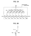
FIG. 3A is an illustration showing a configuration of the variable delay device in FIG. 1 and FIG. 3B is an illustration showing a configuration of a load;
FIG. 4 is an illustration showing a configuration of the control circuit in FIG. 1;
FIG. 5A is a timing chart showing operations of the data transmitter in FIG. 1 in the adjustment period and FIG. 5B is a timing chart showing operations of the data receiver and control circuit in FIG. 1 in the adjustment period;
FIG. 6A is a timing chart showing operations of the data transmitter in FIG. 1 in the data transmission period and FIG. 6B is a timing chart showing operations of the data receiver and control circuit in FIG. 1 in the data transmission period;
FIG. 7 is an illustration showing a configuration of a conventional data transmission system;
FIG. 8 is an illustration showing a configuration of the data transmitter in FIG. 7;
FIG. 9 is an illustration showing a configuration of the data receiver in FIG. 7;
FIG. 10A is a timing chart showing operations of the data transmitter in FIG. 7 and FIG. 10B is a timing chart showing operations of the data receiver in FIG. 7; and
FIGS. 11A to 11C are illustrations for explaining problems of the data transmission system in FIG. 7.
DETAILED DESCRIPTION OF THE PREFERRED EMBODIMENTS
Embodiments of the present invention are described below by referring to the accompanying drawings.
FIG. 1 is an illustration showing a configuration of a data transmission system according to an embodiment of the present invention and a portion same as that in FIG. 7 is provided with the same symbol. The data transmission system according to the embodiment of the present invention has a data transmitter 3, variable delay devices 4 a and 4 b, a data receiver 2, and a control circuit 5. A configuration of the data receiver 2 is the same as the configuration shown in FIG. 9.
The data transmitter 3 transmits a reference signal and an adjustment signal having a predetermined phase relation for the reference signal during an adjustment period for adjusting a phase before data transmission and transmits the reference signal and a phase modulation signal having a phase difference related to the value of input data from the reference signal during a data transmission period after the adjustment period.
The variable delay devices 4 a and 4 b are delay means for respectively delaying a reference signal REF and phase modulation signal (or adjustment signal) DATA sent from the data transmitter 3. It is preferable to use the variable delay devices 4 a and 4 b having the same characteristics. This is because the characteristics are changed in the same direction even if the characteristics are changed due to a temperature change or the like.
As shown in FIG. 9, the data receiver 2 has a phase comparator 21 and an RS latch 22. The phase comparator 21 detects the phase difference between a reference signal REF0 and a phase modulation signal (or adjustment signal) DATA0 delayed by the variable delay devices 4 a and 4 b. The RS latch 22 outputs data DOUT having a value related to the detected phase difference. However, in the case of the adjustment period, symbol DATA shows an adjustment signal having a predetermined phase relation for a reference signal REF, symbol DATA0 shows an adjustment signal delayed by the variable delay device 4 b. In the case of the data transmission period, the symbol DATA shows a phase modulation signal having a phase difference related to the value of input data DIN from the reference signal REF and the symbol DATA0 shows a phase modulation signal delayed by the variable delay device 4 b.
The control circuit 5 controls delay values of the variable delay devices 4 a and 4 b during the adjustment period so as to bring the phase relation between the reference signal REF0 and adjustment signal DATA0 received by the receiver 2 into the above predetermined phase relation and keeps delay values of the variable delay devices 4 a and 4 b controlled in the adjustment period during the data transmission period.
FIG. 2 is an illustration showing a configuration of the data transmitter 3 in FIG. 1, in which a portion same as that in FIG. 8 is provided with the same symbol. As shown in FIG. 2, the data transmitter 3 has delay circuits 11 and 12, multiplexers 13 and 14, a NOR circuit 31, and an inverter 32.
In the data transmission period, because an adjustment designation signal ADJ is set to “0”, the data transmitter 3 outputs a phase modulation signal DATA whose one-unit-time phase advances from the phase of the reference signal REF when data DIN is set to “0” and outputs a phase modulation signal DATA whose one-unit-time phase delays from the phase of the reference signal REF when data DIN is set to “1” similarly to the case of the transmitter 1 in FIG. 8. Because the adjustment designation signal ADJ is set to “1” in the adjustment period, the data transmitter 3 outputs an adjustment signal DATA having no phase difference with the reference signal REF.
In this adjustment period, the phase difference between the reference signal REF0 and adjustment signal DATA0 received by the data receiver 2 through the variable delay devices 4 a and 4 b is detected and the variable delay devices 4 a and 4 b are adjusted by the control circuit 5 so as to decrease the phase difference.
FIG. 3A is an illustration showing a configuration of each of the variable delay devices 4 a and 4 b in FIG. 1 and FIG. 3B is an illustration showing a configuration of the load in FIG. 3A. As shown in FIG. 3A, the variable delay devices 4 a and 4 b respectively have inverters 4-1 to 4-8 and loads 4-9 to 4-14. As shown in FIG. 3B, each of the loads 4-9 to 4-14 is constituted of an nMOS transistor 100 and capacity 101. When a control terminal A is set to “0”, the nMOS transistor 100 is turned off and a delay decreases because the capacity 101 is not seen as the load of an inverter.
However, when the control terminal A is set to “1”, the nMOS transistor 100 is turned on and the delay increases because the capacity 101 is seen as the load of the inverter. Actually, a logical value “0” corresponds to a GND and a logical value “1” corresponds to a power supply voltage VDD. It is possible to continuously change a delay value by change a voltage value to be applied to the control terminal A. Therefore, it is possible to change a delay value during IN-OUT by a control terminal CNT.
FIG. 4 is an illustration showing a configuration of the control circuit 5 in FIG. 1. As shown in FIG. 4, the control circuit 5 has resistances 5-1 to 5-3, a capacity 5-4, transistors 5-5 to 5-8, and an inverter 5-9. A predetermined voltage is generated as an output VREF of the control circuit 5 through resistance division and input to the control terminal CNT of the variable delay device 4 a to make the delay value of the variable delay device 4 a predetermined.
The input DIN of the control circuit 5 is connected to the output DOUT of the data receiver 2. In the adjustment period, the adjustment designation signal ADJ is set to “1”. When the phase of the adjustment signal DATA0 advances from the reference signal REF0, the input DIN of the control circuit 5 is set to “0”, the capacity 5-4 is charged, and the potential of the output CNT of the control circuit 5 rises. Therefore, the delay value of the variable delay device 4 b increases and the phase difference between the reference signal REF0 and the adjustment signal DATA0 decreases. When the phase of the adjustment signal DATA0 delays from the reference signal REF0, the input DIN of the control circuit 5 is set to “1”, the capacity 5-4 is discharged, and the potential of the output CNT of the control circuit 5 lowers. Therefore, the delay value of the variable delay device 4 b decreases and the phase difference between the reference signal REF0 and the adjustment signal DATA0 decreases.
It is possible to decrease the phase difference between the reference signal REF0 and the adjustment signal DATA0 to zero by the above operations of the control circuit 5. When the adjustment designation signal ADJ is set to “0” in the data transmission period, a route for charging and discharging the capacity 5-4 disappears. Therefore, the potential of the output CNT of the control circuit 5 is held by the capacity 5-4. That is, in the data transmission period, the delay value of the variable delay device 4 b is kept at a value controlled in the adjustment period.
It is possible to properly change the number of stages of the loads and inverters of the variable delay devices 4 a and 4 b and the resistance and capacity of the control circuit 5 in accordance with a delay adjustment value or phase comparison accuracy.
Operations of the data transmission system of the embodiment of the present invention are described by referring to the accompanying drawings.
Operations in the adjustment period for adjusting a case in which the reference signal REF and phase modulation signal DATA are displaced as shown in FIGS. 11B and 11C so as to become the ideal state in FIG. 11A are described by referring to FIGS. 5A and 5B. FIG. 5A is a timing chart showing operations of the data transmitter 3 in the adjustment period and FIG. 5B is a timing chart showing operations of the data receiver 2 and control circuit 5 in the adjustment period.
As shown in FIG. 5A, because the adjustment designation signal ADJ is set to “1”, the reference signal REF and adjustment signal DATA having no phase difference are generated. This is realized by inputting a signal CLK having a base frequency to the multiplexers 13 and 14 not through the delay circuits as shown in FIG. 2. The reference signal REF and the adjustment signal DATA having no phase difference may be displaced as shown in FIGS. 11B and 11C due to the fluctuation of actual transmission lines or circuits.
As shown in FIG. 5B, when the reference signal REF0 and adjustment signal DATA0 input to the data receiver 2 are displaced, the displacement is detected by the phase comparator 21 as the phase difference between the reference signal REF0 and the adjustment signal DATA0 and the output DOUT corresponding to a comparison result by the phase comparator 21 is output from the RS latch 22. Then, the control circuit 5 adjusts the variable delay devices 4 a and 4 b provided to the transmission lines between the data transmitter 3 and the data receiver 2 in accordance with the output DOUT of the data receiver 2 so that the phase difference decreases. In FIG. 5B, initial values of the outputs VREF and CNT of the control circuit 5 are set to VDD/2.
Then, operations in the data transmission period are described below by referring to FIGS. 6A and 6B. FIG. 6A is a timing chart showing operations of the data transmitter 3 in the data transmission period and FIG. 6B is a timing chart showing operations of the data receiver 2 and control circuit 5 in the data transmission period.
In the data transmission period, the adjustment designation signal ADJ which is set to “0” is input to the data transmitter 3 and control circuit 5. As shown in FIG. 6A, the data transmitter 3 receives the signal CLK having the base frequency, delays the signal CLK by one unit time tD1 by the delay circuit 11, and outputs the signal CLK as the reference signal REF through the multiplexer 13. Moreover, the signal CLK is input to the multiplexer 14 and the delay circuit 12 and the signal delayed by two unit times tD2 is also input to the multiplexer 14.
When the input data DIN is set to “0”, the multiplexer 14 selects the signal CLK (signal not delayed) and outputs it as the phase modulation signal DATA. However, when the data DIN is set to “1”, the signal CLK delayed through the delay circuit 12 by two unit times tD2 is selected and output as the phase modulation signal DATA. Therefore, when the data DIN is set to “0”, the phase modulation signal DATA whose phase advances by one unit time tD1 from the reference signal REF is transmitted and when the data DIN is set to “1”, the phase modulation signal DATA whose phase is delayed by one unit time tD1 from the reference signal REF is transmitted.
The data receiver 2 receives the reference signal REF0 and phase modulation signal DATA0 incoming through the variable delay devices 4 a and 4 b and their phases are compared by the phase comparator 21. As shown in FIG. 6B, because the control circuit keeps its outputs VREF and CNT at voltage values adjusted in the adjustment period, the phase relation between the reference signal REF0 and the phase modulation signal DATA0 received by the data receiver 2 keeps the phase relation between the reference signal REF and the phase modulation signal DATA.
The phase comparator 21 detects the phase difference between the reference signal REF0 and the phase modulation signal DATA0 When the phase of the phase modulation signal DATA0 advances from the phase of the reference signal REF0, the phase comparator 21 outputs the phase advance detection signal R having the pulse width equivalent to the phase difference between the reference signal REF0 and the phase modulation signal DATA0. Moreover, when the phase of the phase modulation signal DATA0 delays from the phase of the reference signal REF0, the phase comparator 21 outputs the phase delay detection signal S having the pulse width equivalent to the phase difference between the phase modulation signal DATA0 and the reference signal REF0.
When the phase delay detection signal S is applied to a set input terminal, the RS latch 22 sets the output DOUT to “1” but when the phase advance detection signal R is applied to a reset input terminal, it sets the output DOUT to “0”. Then, it is possible to obtain transmitted data from the level of the demodulation output DOUT.
As described above, in the case of the embodiment of the present invention, by decreasing skews between the reference signal and the phase modulation signal due to the delay fluctuation of LSIs or transmission lines and equalizing the phase relation between the reference signal and the phase modulation signal received by the receiver with the phase relation for transmission, it is possible to enlarge the margin to jitter or noise. Therefore, it is possible to prevent malfunctions and accelerate data transmission.
The control circuit 5 can be included in the data receiver 2.