US8013665B2 - Semiconductor device - Google Patents
Semiconductor device Download PDFInfo
- Publication number
- US8013665B2 US8013665B2 US11/957,560 US95756007A US8013665B2 US 8013665 B2 US8013665 B2 US 8013665B2 US 95756007 A US95756007 A US 95756007A US 8013665 B2 US8013665 B2 US 8013665B2
- Authority
- US
- United States
- Prior art keywords
- electrode
- capacitor element
- semiconductor device
- capacitor
- film
- Prior art date
- Legal status (The legal status is an assumption and is not a legal conclusion. Google has not performed a legal analysis and makes no representation as to the accuracy of the status listed.)
- Expired - Fee Related, expires
Links
Images


Classifications
-
- H—ELECTRICITY
- H01—ELECTRIC ELEMENTS
- H01L—SEMICONDUCTOR DEVICES NOT COVERED BY CLASS H10
- H01L27/00—Devices consisting of a plurality of semiconductor or other solid-state components formed in or on a common substrate
- H01L27/02—Devices consisting of a plurality of semiconductor or other solid-state components formed in or on a common substrate including semiconductor components specially adapted for rectifying, oscillating, amplifying or switching and having at least one potential-jump barrier or surface barrier; including integrated passive circuit elements with at least one potential-jump barrier or surface barrier
- H01L27/04—Devices consisting of a plurality of semiconductor or other solid-state components formed in or on a common substrate including semiconductor components specially adapted for rectifying, oscillating, amplifying or switching and having at least one potential-jump barrier or surface barrier; including integrated passive circuit elements with at least one potential-jump barrier or surface barrier the substrate being a semiconductor body
-
- H—ELECTRICITY
- H02—GENERATION; CONVERSION OR DISTRIBUTION OF ELECTRIC POWER
- H02M—APPARATUS FOR CONVERSION BETWEEN AC AND AC, BETWEEN AC AND DC, OR BETWEEN DC AND DC, AND FOR USE WITH MAINS OR SIMILAR POWER SUPPLY SYSTEMS; CONVERSION OF DC OR AC INPUT POWER INTO SURGE OUTPUT POWER; CONTROL OR REGULATION THEREOF
- H02M3/00—Conversion of dc power input into dc power output
- H02M3/02—Conversion of dc power input into dc power output without intermediate conversion into ac
- H02M3/04—Conversion of dc power input into dc power output without intermediate conversion into ac by static converters
- H02M3/06—Conversion of dc power input into dc power output without intermediate conversion into ac by static converters using resistors or capacitors, e.g. potential divider
- H02M3/07—Conversion of dc power input into dc power output without intermediate conversion into ac by static converters using resistors or capacitors, e.g. potential divider using capacitors charged and discharged alternately by semiconductor devices with control electrode, e.g. charge pumps
- H02M3/073—Charge pumps of the Schenkel-type
-
- G—PHYSICS
- G11—INFORMATION STORAGE
- G11C—STATIC STORES
- G11C5/00—Details of stores covered by group G11C11/00
- G11C5/14—Power supply arrangements, e.g. power down, chip selection or deselection, layout of wirings or power grids, or multiple supply levels
Definitions
- the present invention relates to a semiconductor device having a boosting circuit, in particular, a semiconductor device having a boosting circuit which supplies a potential higher than power source voltage.
- a boosting circuit is used for a variety of purposes, for example, for a CCD driver circuit, an organic EL driver circuit, a low-temperature polysilicon liquid crystal driver circuit, a white light emitting diode driver circuit, an RF circuit, and a multiple power source system.
- reduction in voltage in a semiconductor device such as a flash memory is accompanied by boosting power source voltage for obtaining high voltage necessary for writing or erasing data.
- a boosting circuit which has a small area and efficiently generates high voltage has been expected in various fields, with the higher integration of integrated circuits of semiconductor devices.
- a MOS capacitor using a semiconductor substrate having a conductivity type or an insulating film having high dielectric constant, as a capacitor (a capacitor element), is proposed (for example, Reference 1: Japanese Published Patent Application No. 2003-297936).
- a semiconductor substrate having a conductivity type is used for one of electrodes of a MOS capacitor, and a conductive film corresponding to a gate electrode is used for the other of the electrodes, and an insulating film corresponding to a gate insulating film of a transistor is provided between the two electrodes to increase capacitance per unit area.
- an impurity element is necessary to be selectively introduced into a semiconductor film to be the one of the electrodes of the capacitor element after forming the semiconductor film over a substrate.
- TFT thin film transistor
- an impurity element is necessary to be selectively introduced into a semiconductor film to be the one of the electrodes of the capacitor element after forming the semiconductor film over a substrate.
- a semiconductor device of the present invention includes a plurality of rectifying elements, which is connected in series and has a rectifying function from a first input terminal portion to an output terminal portion; a first wiring and a second wiring, which are connected to a second input terminal portion, into which a signal and a signal obtained by inverting the signal are respectively input; and a boosting circuit including capacitor elements each having a first electrode, an insulating film, and a second electrode.
- the first electrode is connected to an output portion of a rectifying element of the plurality of rectifying elements and an input portion of another rectifying element of the plurality of rectifying elements, which is adjacent to the rectifying element;
- the second electrode is connected to the first wiring or the second wiring;
- the plurality of capacitor elements includes a capacitor element in which the first electrode and the second electrode are formed using conductive films, and a capacitor element in which at least the second electrode is formed using a semiconductor film; and, in the plurality of capacitor elements, at least a capacitor element in a first stage is a capacitor element in which the first electrode and the second electrode are formed using conductive films.
- the semiconductor device of the present invention can have a structure in which the rectifying element is a diode-connected thin film transistor; and a gate electrode of the thin film transistor, the first electrode of the capacitor element in the first stage, and a first electrode of the capacitor element in which the second electrode is provided using a semiconductor film, are formed using a same material.
- a semiconductor device of the present invention includes a plurality of rectifying elements, which is connected in series and includes at least a first rectifying element, a second rectifying element, and a third rectifying element which have a rectifying function from a first input terminal portion to an output terminal portion; a first wiring and a second wiring, which are connected to a second input portion; and a boosting circuit including a plurality of capacitor elements having a first capacitor element provided in a first stage and a second capacitor element provided in a second stage.
- the plurality of capacitor elements includes a capacitor element in which the first electrode and the second electrode are formed using conductive films, and a capacitor element in which at least the second electrode is formed using a semiconductor film; the first electrode of the first capacitor element is connected to an output portion of the first rectifying element and an input portion of the second rectifying element; the second electrode of the first capacitor element is connected to the first wiring; the first electrode of the second capacitor element is connected to an output portion of the second rectifying element and an input portion of the third rectifying element; the second electrode of the second capacitor element is connected to the second wiring; and at least the first capacitor element is a capacitor element in which the first electrode and the second electrode are formed using conductive films.
- the second capacitor element may be a capacitor element in which the second electrode is formed using a semiconductor film.
- the present invention by providing a capacitor element of a thin film transistor type for each capacitor element of a boosting circuit, the area of the boosting circuit can be reduced. Further, by providing one of electrodes of a capacitor element using a semiconductor film formed in the same step as a semiconductor film forming a channel formation region of a TFT, a step of introducing an impurity element into a semiconductor film is not necessary, a manufacturing process can be simplified, and the number of masks can be reduced, leading to low cost.
- capacitor elements in plural stages which are provided for a boosting circuit by providing at least a capacitor element in a first stage using a capacitor element in which two electrodes are formed using conductive films and providing capacitor elements in other stages using capacitor elements using semiconductor films, electric charge can be stored even in the case where voltage applied to one end of the capacitor element in the first stage is lower than threshold voltage of the capacitor element using a semiconductor film.
- the area of the boosting circuit can be reduced and a boosting circuit can operate appropriately.
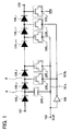
- FIG. 1 is a diagram showing an example of a semiconductor device of the present invention
- FIG. 2 is a view showing an example of a semiconductor device of the present invention
- FIG. 3 is a view showing an example of a semiconductor device of the present invention.
- FIG. 4 is a view showing an example of a semiconductor device of the present invention.
- FIG. 5 is a view showing an example of a semiconductor device of the present invention.
- FIGS. 6A to 6C are views showing an example of a method for manufacturing a semiconductor device of the present invention.
- FIGS. 7A to 7C are views showing an example of a method for manufacturing a semiconductor device of the present invention.
- FIG. 8 is a diagram showing an example of a semiconductor device of the present invention.
- FIG. 9 is a diagram showing an example of a semiconductor device of the present invention.
- FIGS. 10A to 10H are views each showing an example of a usage of a semiconductor device of the present invention.
- This embodiment mode describes a structural example of a boosting circuit of a semiconductor device of the present invention with reference to the drawings.
- a semiconductor device described in this embodiment mode includes a boosting circuit formed by using a capacitor element in which an insulating film is provided between two conductive films and a capacitor element of a thin film transistor type.
- a capacitor element of a thin film transistor type refers to a capacitor element including a second electrode formed using a semiconductor film corresponding to a semiconductor film forming a channel formation region of a TFT; an insulating film formed using an insulating film corresponding to a gate insulating film of the TFT; and a first electrode formed using a conductive film corresponding to a gate electrode of the TFT.
- the capacitor element of a thin film transistor type is formed in the same step as a TFT serving as a switch or the like provided for another integrated circuit in a semiconductor device.
- a specific structure of a semiconductor device equipped with a boosting circuit described in this embodiment mode is described.
- a boosting circuit in a semiconductor device described in this embodiment mode is formed by combining a capacitor element (bipolar) in which an insulating film is provided between two conductive films, and a capacitor element (unipolar) of a thin film transistor type in which at least one of electrodes is formed using a semiconductor film.
- the boosting circuit includes a first input terminal portion 101 , a second input terminal portion 102 , an output terminal portion 103 , a first capacitor element 205 —1 to an n-th capacitor element 205 —n , a first diode 104 —1 to an n-th diode 104 —n , and an inverter 106 .
- the first diode 104 —1 to the n-th diode 104 —n are connected in series and are rectifying elements have a function of rectifying current from the first input terminal portion 101 to the output terminal portion 103 .
- the first input terminal portion 101 is connected to one of electrodes of the first diode 104 —1
- the other of the electrodes of the first diode 104 —1 is connected to one of electrodes of the second diode 104 —2 and an electrode of the first capacitor element 205 —1 (see FIG. 1 ).
- the capacitor element of a thin film transistor type has a structure in which one of electrodes (a second electrode) is formed using a semiconductor film and the other of the electrodes (a first electrode) is formed using a conductive film.
- the second electrode is formed using a semiconductor film corresponding to a semiconductor film forming a channel formation region of a TFT which is provided for another integrated circuit;
- the first electrode is formed using a conductive film corresponding to a gate electrode of the TFT;
- the insulating film is formed using an insulating film corresponding to a gate insulating film of the TFT. Accordingly, a step of introducing an impurity element into a semiconductor film to be the second electrode is not necessary, and thus, a manufacturing process can be simplified.
- the second input terminal portion 102 is connected to a first wiring 107 a and a second wiring 107 b .
- the first wiring 107 a is connected to one of electrodes of each of the capacitor elements in odd-numbered stages, such as the first capacitor element 205 —1 and the third capacitor element 205 —3 .
- the second wiring 107 b is connected to one of the electrodes of each of the capacitor elements in even-numbered stages, such as the second capacitor element 205 —2 and the fourth capacitor element 205 —4 .
- Predetermined voltage for example, power source voltage
- Predetermined voltage is input to the first input terminal portion 101
- boosted voltage is output from the output terminal portion 103 .
- a clock signal is input to the second input terminal portion 102
- a signal (“High” or “Low”) and a signal obtained by inverting the signal by the inverter 106 are input to the first wiring 107 a and the second wiring 107 b , respectively.
- one of “High” and “Low” is applied to one of the electrodes of each of the capacitor elements in the odd-numbered stages (the first capacitor element 205 —1 , the third capacitor element 205 —3 , and the like) connected to the first wiring 107 a
- the other of “High” and “Low” is applied to one of the electrodes of each of the capacitor elements in the even-numbered stages (the second capacitor element 205 —2 , the fourth capacitor element 205 —4 , and the like) connected to the second wiring 107 b.
- the inverter 106 is provided so as to be connected to the second input terminal portion 102 and one of the electrodes of the second capacitor element 205 —2 .
- a structure may be employed, in which clock signals having different phases are input without providing the inverter 106 .
- At least a capacitor element in a first stage (here, the first capacitor element 205 —1 ) has a structure in which an insulating film is formed between a first conductive film and a second conductive film, and other capacitor elements (here, the second capacitor element 205 —2 to the n-th capacitor element 205 —n ) each have a structure of a thin film transistor type.
- a capacitor element in a first stage refers to a capacitor element in which the lowest potential is stored among a plurality of capacitor elements provided for a boosting circuit.
- the first capacitor element 205 —1 which is connected to an output portion of the first diode 104 —1 which is a diode in the first stage and is connected to the first input terminal portion 101 and an input portion of the second diode 104 —2 , is the capacitor element in the first stage.
- a structure may be employed, in which the capacitor element in the first stage is connected to not an output portion but an input portion of the first diode 104 —1 .
- the boosting circuit is provided with not only a capacitor element having a structure in which an insulating film is provided between a first conductive film and a second conductive film but also a capacitor element of a thin film transistor type. Accordingly, the insulating film forming the capacitor element can be formed to be thinned, and thus, the area of the capacitor element can be reduced. Further, by providing a capacitor element of a thin film transistor type, a step of introducing an impurity element into a semiconductor film overlapping with the other of electrodes in advance can be omitted, and thus, a process can be simplified, which leads to low cost. That is, with the structure shown in FIG. 1 , reduction in area of the capacitor element and appropriate operation of the boosting circuit can be realized.
- At least the first capacitor element 205 —1 has a structure in which an insulating film, which is different from a gate insulating film, is formed between conductive films.
- the first capacitor element 205 —1 and other capacitor elements here, the second capacitor element 205 —2 to the n-th capacitor element 205 —n
- the first capacitor element 205 —1 and the second capacitor element 205 —2 have different element areas.
- a gate insulating film is thinner than an insulating film which is different from a gate insulating film, and the first capacitor element 205 —1 becomes larger in area than the second capacitor element 205 —2 .
- first diode 104 —1 to the n-th diode 104 —n may be elements each having a rectifying function, and each of the first diode 104 —1 to the n-th diode 104 , can be formed using, for example, a PN diode, a PIN diode, a Schottky diode, a MIM (metal insulator metal) diode, a MIS (metal insulator semiconductor) diode, a diode-connected transistor, or the like.
- the boosting circuit shown in FIG. 1 is a circuit including n pieces of the diodes 104 —1 to 104 —n , n pieces of the capacitor elements 205 —1 to 205 —n , and the inverter 106 , and can obtain output voltage of (VIN ⁇ VF) ⁇ n by inputting a clock signal, given that VIN is input voltage and VF is forward voltage of the diode.
- the clock signal which is output from the second input terminal portion 102 is input to one end of each of the capacitor elements 205 —1 and 205 —3 . Further, the clock signal which is output from the second input portion 102 and then inverted by the inverter 106 is input to one end of the capacitor element 205 —2 .
- An anode for the diode 104 —2 is denoted by A
- a cathode for the diode 104 —2 is denoted by B.
- Electric charge is supplied to each of the anode A and the cathode B with the use of the clock signal and the clock signal obtained by inverting the clock signal, respectively.
- VF forward voltage
- the boosted voltage is (VIN ⁇ VF).
- output voltage is boosted by (VIN ⁇ VF) in every stage.
- FIG. 1 n stages of circuits are connected in series; thus, output voltage is increased by (VIN ⁇ VF) ⁇ n. In this manner, the circuit shown in FIG. 1 serves as a boosting circuit.
- FIG. 2 is a schematic view of a top view of the boosting circuit of the semiconductor device
- FIG. 3 is a schematic view of a cross-sectional view taken along lines A 1 -A 2 and B 1 -B 2 in FIG. 2
- FIGS. 2 and 3 show the case where the diodes in FIG. 1 are formed using diode-connected thin film transistors.
- the semiconductor device shown in FIGS. 2 and 3 includes semiconductor films 113 and 114 provided to have island-like shapes over a substrate 110 with an insulating film 111 interposed between the semiconductor films 113 and 114 , and the substrate 110 ; conductive films 117 and 118 provided over the semiconductor films 113 and 114 with a gate insulating film 115 interposed between the conductive films 117 and 118 and the semiconductor films 113 and 114 ; a first conductive film 218 provided over the gate insulating film 115 ; an insulating film 119 provided to cover the gate insulating film 115 and the conductive films 117 and 118 ; and conductive films 120 a , 120 b , and 121 b , and a second conductive film 231 provided over the insulating film 119 .
- the semiconductor film 113 includes a channel formation region 113 a provided below the conductive film 117 , and impurity regions 113 b which are provided to be separated from each other by the channel formation region 113 a .
- the conductive films 120 a and 120 b are electrically connected to the impurity regions 113 b which are provided to be separated from each other.
- One of the impurity regions 113 b which are provided to be separated from each other may be referred to as a source region or a drain region, and one of the conductive films 120 a and 120 b may be referred to as source electrode or a drain electrode.
- the conductive film 117 and the conductive film 120 a serving as a source electrode or a drain electrode are electrically connected to each other, and the thin film transistor serves as a diode.
- the conductive film 120 a corresponds to one of the electrodes of the first diode 104 —1 in FIG. 1
- the conductive film 120 b corresponds to the other of the electrodes of the first diode 104 —1 in FIG. 1 .
- the semiconductor film 114 includes a region 114 a provided below the conductive film 118 , and impurity regions 114 b which are provided to be separated from each other by the region 114 a .
- the conductive film 121 b is electrically connected to the impurity regions 114 b which are provided to be separated from each other.
- the impurity regions 114 b provided to be separated from each other are provided at the same time as the impurity regions 113 b serving as a source region and a drain region of the semiconductor film 113 .
- the region 114 a is formed in the same step as the channel formation region 113 a of the semiconductor film 113 . Therefore, the region 114 a and the channel formation region 113 include almost the same impurity element.
- the conductive film 121 b connected to the impurity regions 114 b which are provided to be separated from each other is provided.
- the semiconductor film 114 corresponds to the second electrode of each of the second capacitor element 205 —2 to the n-th capacitor element 205 —n in FIG. 1 .
- the conductive film 118 corresponds to the first electrode of each of the second capacitor element 205 —2 to the n-th capacitor element 205 , in FIG. 1 .
- the impurity regions 114 b of the semiconductor film 114 are electrically connected to the second wiring 107 b through the conductive film 121 b.
- the first capacitor element 205 —1 can be formed using the first conductive film 218 , the insulating film 119 , and the second conductive film 231 .
- the first conductive film 218 can be formed using the same material as the conductive film 117 and the conductive film 118
- the second conductive film 231 can be formed using the same material as the conductive films 120 a , 120 b , and 121 b.
- a gate insulating film as an insulating film of a capacitor element, the area of the capacitor element can be reduced, whereby the semiconductor device can be made smaller.
- one of electrodes thereof is formed using a semiconductor film corresponding to a semiconductor film forming a channel formation region of a TFT provided for an integrated circuit, whereby a manufacturing process can be simplified and the number of masks can be reduced, which leads to low cost.
- At least a capacitor element in a first stage is provided to have a structure in which two electrodes are provided using conductive films, whereby reduction in area of the capacitor element and appropriate operation of the boosting circuit can be realized.
- FIGS. 2 and 3 show the case where the conductive film 121 b electrically connected to the impurity regions 114 b does not overlap with the conductive film 118 , the conductive film 121 b may be provided to cover the conductive film 118 (see FIGS. 4 and 5 ). In this case, reduction in area of the capacitor element and improvement in characteristics due to increase in capacitance are possible.
- FIG. 4 is a schematic view of a top view of a boosting circuit of a semiconductor device
- FIG. 5 is a schematic view of a cross-sectional view taken along lines A 1 -A 2 and B 1 -B 2 in FIG. 4 .
- the structure of the semiconductor device described in this embodiment mode can be implemented by being freely combined with the structures of the semiconductor devices in other embodiment modes in this specification.
- an insulating film 111 which serves as a base is formed over a substrate 110 .
- the substrate 110 may be a glass substrate, a quartz substrate, a metal or stainless steel substrate which has an insulating film formed over one surface, a plastic substrate which has sufficient heat resistance to withstand processing temperatures of this process, or the like.
- a substrate 110 there are no large restrictions on its area or shape; therefore, when, for example, a rectangular substrate which has a side of one meter or more is used as the substrate 110 , productivity can be improved markedly.
- a merit such as this is a large advantage compared with the case of using a circular silicon substrate.
- an SOI substrate Silicon On Insulator
- a separation layer is used between the substrate 110 and the insulating film 111 , a layer having a thin film transistor can be transposed to a substrate over which a conductive film or the like is formed, and as a result, a connection between a conductive film which is connected to the thin film transistor, and the conductive film which is over the substrate to which the conductive film is transposed, can be simplified.
- a layer which includes an oxide of silicon or a nitride of silicon is formed as the insulating film 111 using a sputtering method, a plasma CVD method, or the like.
- An oxide of silicon is a material which includes silicon (Si) and oxygen (O), and corresponds to silicon oxide, silicon oxynitride, silicon nitride oxide, and the like.
- a nitride of silicon is a material which includes silicon and nitrogen (N), and corresponds to silicon nitride, silicon oxynitride, silicon nitride oxide, and the like.
- the insulating film which serves as the base may be a single layer or a stack of layers.
- a silicon nitride oxide layer is formed as a first layer and a silicon oxynitride layer is formed as a second layer.
- a silicon oxide layer may be formed as a first insulating film
- a silicon nitride oxide layer may be formed as a second insulating film
- a silicon oxynitride layer may be formed as a third insulating film.
- a silicon oxynitride layer may be formed as a first insulating film
- a silicon nitride oxide layer may be formed as a second insulating film
- a silicon oxynitride layer may be formed as a third insulating film.
- the insulating film which serves as the base functions as a blocking film which prevents penetration of impurities from the substrate 110 .
- an amorphous semiconductor film (for example, a layer including amorphous silicon) is formed over the insulating film 111 .
- the amorphous semiconductor film is formed to a thickness of 25 to 200 nm (preferably 30 to 150 nm) using a sputtering method, an LPCVD method, a plasma CVD method, or the like.
- the amorphous semiconductor film is crystallized using a laser crystallization method, a thermal crystallization method which employs RTA or an annealing furnace, a thermal crystallization method which employs a metal element which promotes crystallization, a method in which a laser crystallization method is combined with a thermal crystallization method which employs a metal element which promotes crystallization, or the like to form a crystalline semiconductor film.
- the obtained crystalline semiconductor film is patterned into a desired shape to form crystalline semiconductor films 113 and 114 (see FIG. 6A ).
- a plasma CVD method is used to form an amorphous semiconductor film with a thickness of 66 nm.
- a solution which includes nickel, which is a metal element that promotes crystallization is retained on the amorphous semiconductor film, and the amorphous semiconductor film is then subjected to dehydrogenation treatment (at 500° C. for one hour) and thermal crystallization treatment (at 550° C. for four hours) to form a crystalline semiconductor film.
- dehydrogenation treatment at 500° C. for one hour
- thermal crystallization treatment at 550° C. for four hours
- laser light irradiation is performed as necessary and patterning treatment which employs a photolithography method is performed, whereby the crystalline semiconductor films 113 and 114 are formed.
- a continuous wave or pulsed gas laser or solid-state laser is used.
- a gas laser an excimer laser, a YAG laser, a YVO 4 laser, a YLF laser, a YAlO 3 laser, a glass laser, a ruby laser, a Ti:sapphire laser, or the like is used.
- a solid state laser a laser which employs a crystal, such as YAG, YVO 4 , YLF, or YAlO 3 , which is doped with Cr, Nd, Er, Ho, Ce, Co, Ti, or Tm is used.
- a metal element which promotes crystallization is used to crystallize the amorphous semiconductor film, while there are advantages in that crystallization can be performed at a low temperature in a short period of time and the direction of crystals is uniform, there are also drawbacks in that because metal element remains on the crystalline semiconductor film, off-state current increases and TFT characteristics are not stable. Therefore, preferably an amorphous semiconductor film which functions as a gettering site is formed over the crystalline semiconductor film.
- the amorphous semiconductor layer is formed using a sputtering method by which argon can be included in the amorphous semiconductor layer at a high concentration. Then, heat treatment (an RTA method, thermal annealing which employs an annealing furnace, or the like) is performed and the metal element is diffused into the amorphous semiconductor film. Subsequently, the amorphous semiconductor film which includes the metal element is removed. Thus, the amount of metal element included in the crystalline semiconductor film can be reduced or metal element included in the crystalline semiconductor film can be removed from the crystalline semiconductor film.
- the gate insulating film 115 includes an oxide of silicon or a nitride of silicon and is formed by a plasma CVD method, a sputtering method, or the like as a single layer or a stack of layers. Specifically, a layer including silicon oxide, a layer including silicon oxynitride, or a layer including silicon nitride oxide is formed as a single layer, or such layers are used to form a stack of layers.
- the first conductive film is formed to a thickness of 20 to 100 nm by a plasma CVD method, a sputtering method, or the like.
- the second conductive film is formed to a thickness of 100 to 400 nm by a plasma CVD method, a sputtering method, or the like.
- the first conductive film and the second conductive film are formed using any one of the elements tantalum (Ta), tungsten (W), titanium (Ti), molybdenum (Mo), aluminum (Al), copper (Cu), chromium (Cr), niobium (Nb), and the like, or of an alloy material or a compound material which includes such an element as a main constituent.
- they may be formed of a semiconductor material typified by polycrystalline silicon doped with an impurity element such as phosphorus.
- Examples which can be given of combinations of the first conductive film and the second conductive film include a tantalum nitride layer and a tungsten (W) layer, a tungsten nitride layer and a tungsten layer, a molybdenum nitride layer and a molybdenum (Mo) layer, and the like.
- Tungsten and tantalum nitride have high heat resistance, so when they are used to form the first conductive film and the second conductive film, subsequent to the formation of the two layers, heat treatment for thermal activation can be performed.
- a stacked structure which includes a molybdenum layer, an aluminum layer, and another molybdenum layer may be used.
- a resist mask is formed by a photolithography method, and an etching treatment is performed on the first conductive film and the second conductive film to form conductive films 117 and 118 which serve as gate electrodes and a conductive film 218 serving as a first electrode of a capacitor element (see FIG. 6C ).
- a resist mask is formed by a photolithography method, and desired n-type or p-type impurity regions 113 b and 114 b , a channel forming region 113 a , and a region 114 a are formed in the crystalline semiconductor films 113 and 114 using an ion doping method or an ion implantation method.
- an element which belongs to Group 15 of the periodic table may be used as an impurity element which imparts n-type conductivity.
- phosphorus (P) or arsenic (As) is used as an impurity element and is added to form n-type impurity regions.
- a resist mask is formed using a photolithography method, and an impurity element which imparts p-type conductivity, for example, boron (B), is added to a desired crystalline semiconductor film to form a p-type impurity region.
- an impurity element which imparts p-type conductivity for example, boron (B)
- B boron
- an insulating film 119 is formed so as to cover the gate insulating film 115 and the conductive films 117 and 118 .
- the insulating film 119 is formed by a sputtering method, a CVD method, an SOG method, a droplet discharge method, or the like, using an inorganic material such as an oxide of silicon or a nitride of silicon; an organic material such as a polyimide, a polyamide, benzocyclobutene, an acrylic, an epoxy, or a siloxane; or the like.
- Siloxane has a skeleton structure formed of bonds between silicon (Si) and oxygen (O).
- an organic group containing at least hydrogen (for example, an alkyl group or an aromatic hydrocarbon) is used as a substituent.
- a fluoro group may also be used as a substituent.
- a fluoro group and an organic group containing at least hydrogen may be used as a substituent.
- the insulating film which covers the gate insulating film and the conductive films may be a single layer or a stack of layers. When a three-layer structure is used, a layer including silicon oxide may be formed as a first layer of the insulating film, a layer including a resin may be formed as a second layer of the insulating film, and a layer including silicon nitride may be formed as a third layer of the insulating film.
- heat treatment for restoring the crystallinity of the semiconductor films, activating an impurity element which has been added to the semiconductor films, or hydrogenating the semiconductor films may be performed.
- heat treatment thermal annealing, a laser annealing method, an RTA method, or the like may be used.
- the insulating film 119 is etched by a photolithography method to form contact holes which expose the impurity regions 113 b and 114 b (see FIG. 7A ). Subsequently, a conductive film 154 is formed so that the contact holes are filled (see FIG. 7B ).
- the conductive film 154 is formed as a single layer or as stacked layers by a plasma CVD method, a sputtering method, or the like using any of the elements titanium (Ti), aluminum (Al), or neodymium (Nd), or an alloy material or a compound material which contains one of the above-mentioned elements as its main constituent.
- An alloy material containing aluminum as its main constituent corresponds to, for example, a material which has aluminum as its main constituent and includes nickel, or an alloy material which has aluminum as its main constituent and includes nickel and one or both of carbon and silicon.
- the conductive films 120 a to 121 b may employ, for example, a stacked layer structure which includes a barrier layer, an aluminum-silicon (Al—Si) layer, and another barrier layer; or a stacked layer structure which includes a barrier layer, an aluminum-silicon (Al—Si) layer, a titanium nitride layer, and another barrier layer.
- a barrier layer corresponds to a thin film formed from titanium, a nitride of titanium, molybdenum, or a nitride of molybdenum.
- Aluminum and aluminum silicon have low resistance and are inexpensive; therefore, they are ideal materials for forming the conductive films 120 a to 121 b .
- a hillock of aluminum or aluminum silicon can be prevented when upper and lower barrier layers are provided.
- a barrier layer is formed from titanium, which is a highly reducible element, even when a thin natural oxide film forms over the crystalline semiconductor film, the natural oxide film is reduced, and therefore good contact with the crystalline semiconductor film can be obtained.
- the conductive film 154 is selectively etched to form conductive films 120 a , 120 b , 121 a , and 121 b , each of which serves as a source electrode or a drain electrode, and a conductive film 231 serving as a second electrode of the capacitor element (see FIG. 7C ).
- a semiconductor device which includes a thin film transistor having the semiconductor film 113 , the insulating film 115 to be a gate insulating film, and the conductive film 117 to be a gate electrode; a capacitor element having the conductive film 218 to be a first electrode, the insulating film 119 , and the conductive film 231 to be a second electrode; and a capacitor element of a thin film transistor type, which has the semiconductor film 114 to be a second electrode, the insulating film 115 , and the conductive film 118 to be a first electrode.
- a thin film transistor, a capacitor element of a thin film transistor type, and a capacitor element in which two electrodes are formed using conductive films can be manufactured in the same steps.
- This embodiment mode describes a structure of a semiconductor device which can transmit and receive information wirelessly (also referred to as an RFID (radio frequency identification system) tag, an RF tag, an ID tag, an IC tag, a wireless tag, an electronic tag, or a wireless chip) and has a memory with a built-in boosting circuit in the above-described embodiment mode, with reference to the drawings.
- RFID radio frequency identification system
- the semiconductor device described in this embodiment mode has features such as capability of transmitting and receiving information with an external device (a reader/writer) without contact, operation without battery, and superiority in durability and weatherability.
- a memory is often mounted on such a semiconductor device to improve its function.
- One feature of the semiconductor device described in this embodiment mode is that reading and writing data are possible without contact.
- Transmission formats of data are roughly classified into three types, which are: an electromagnetic coupling type which conducts communication through mutual induction by positioning a pair of coils so as to face each other; an electromagnetic induction type which conducts communication through an induction field; and a radio wave type which conducts communication by utilizing radio waves. Any type may be used.
- an antenna used for the data transmission can be provided in two ways: one is that the antenna is provided over a substrate where a plurality of elements and a memory element are provided, and the other is that a terminal portion is provided over a substrate where a plurality of elements and a memory element are provided and an antenna provided over another substrate is connected to the terminal portion.
- This embodiment mode describes a structural example of a semiconductor device of a case of providing an antenna over a substrate provided with a plurality of elements and a memory element, with reference to FIG. 8 .
- a semiconductor device shown in FIG. 8 includes an antenna circuit 401 , a clock generation circuit 404 , a power supply circuit 405 , a control circuit 412 , and a memory circuit 413 over a substrate 400 .
- the antenna circuit 401 includes an antenna 402 and a resonant capacitor 403
- the power supply circuit 405 includes a smoothing circuit 406 and a boosting circuit 407 .
- the smoothing circuit 406 includes a diode 408 which rectifies an alternating signal, and a smoothing capacitor 409
- the boosting circuit 407 includes a group of diodes 410 for boosting voltage, and a group of capacitor elements 411 .
- a data modulation/demodulation circuit, a sensor, and the like may be included.
- second voltage which is higher than voltage used at the time of reading.
- a method for generating the second voltage a method for boosting voltage (first voltage) obtained by smoothing a signal received by an antenna with the use of a boosting circuit, can be used.
- This embodiment mode describes a structure of a battery (an RF (radio frequency) battery) capable of being charged wirelessly, which has a built-in boosting circuit, in the above-described embodiment mode with reference to FIG. 9 .
- An RF battery (a non-contact battery using radio frequency) has features such as capability of charging-up an object without contact, superiority in portability, and the like.
- an RF battery includes a second antenna circuit 502 , a resonant capacitor 503 , a capacitor 504 of a rectifier circuit, a smoothing capacitor 507 , a capacitor 510 for battery, diodes 505 and 506 which rectify an alternating signal, a diode 509 for backflow prevention, a regulator circuit 508 , and a boosting circuit 511 .
- a sensor and the like may be included.
- Electric power output from the power supply 500 is oscillated through the first antenna circuit 501 and received by the second antenna circuit 502 of the RF battery.
- a resonant frequency of the received electric wave is tuned to a specific frequency using the resonant capacitor 503 .
- the received voltage is rectified using the capacitor 504 , the first diode 505 , and the second diode 506 .
- the received voltage is stored in the capacitor 510 through the regulator.
- the RF battery is not charged unless power source voltage (for example, 2 V) exceeds a certain threshold.
- power source voltage for example, 2 V
- the boosting circuit 511 is provided in a subsequent stage of the regulator or provided for a place, which is different from the regulator, over the same circuit, so that electric power can be stored even when voltage less than or equal to threshold voltage is input.
- This embodiment mode describes examples of the application of the semiconductor device capable of transmitting and receiving information wirelessly, in the above-described embodiment mode.
- the semiconductor device of the invention can be used for various applications, and can be applied to any product whose information such as history can be wirelessly obtained by the semiconductor device so that the information can be effectively utilized for production, management, and the like of the product.
- the semiconductor device of the invention can be applied to bills, coins, securities, documents, bearer bonds, packaging containers, books, storage media, personal belongings, means of transportation, foods, clothes, healthcare items, daily commodities, medicines, electronic devices, and the like. Examples of such application will be described with reference to FIGS. 10A to 10H .
- the bills and coins are currency in the market and include notes that are circulating as the real money in specific areas (cash vouchers), memorial coins, and the like.
- the securities include checks, certificates, promissory notes, and the like ( FIG. 10A ).
- the documents include driver's licenses, resident's cards, and the like ( FIG. 10B ).
- the bearer bonds include stamps, rice coupons, various gift coupons, and the like ( FIG. 10C ).
- the packaging containers include paper for wrapping a lunch box or the like, plastic bottles, and the like ( FIG. 10D ).
- the books include documents and the like ( FIG. 10E ).
- the storage media include DVD software, video tapes, and the like ( FIG. 10F ).
- the means of transportation include wheeled cycles or vehicles such as bicycles, vessels, and the like ( FIG. 10G ).
- the personal belongings include shoes, glasses, and the like ( FIG. 10H ).
- the foods include food items, beverages, and the like.
- the clothes include clothing, footwear, and the like.
- the healthcare items include medical devices, health appliances, and the like.
- the daily commodities include furniture, lighting apparatuses, and the like.
- the medicines include medicament, agricultural chemicals, and the like.
- the electronic devices include liquid crystal display devices, EL display devices, television devices (television receivers or thin television receivers), mobile phones, and the like.
- a semiconductor device 80 When a semiconductor device 80 is provided for bills, coins, securities, documents, bearer bonds, and the like, forgery thereof can be prevented. In addition, when the semiconductor device 80 is provided for packaging containers, books, storage media, personal belongings, foods, daily commodities, electronic devices, and the like, the efficiency of an inspection system, a rental shop system, and the like can be improved. Further, when the semiconductor device 80 is provided for means of transportation, healthcare items, medicines, and the like, forgery and theft thereof can be prevented and wrong use of the medicines can be prevented.
- the semiconductor device 80 may be provided by, for example, being attached to the surface of an object or embedded in an object. For example, the semiconductor device 80 may be embedded in paper of a book or embedded in an organic resin of a package.
- the method for manufacturing the semiconductor device described in this embodiment mode can be applied to the semiconductor device in other embodiment modes described in this specification.
Abstract
Description
Claims (13)
Priority Applications (1)
| Application Number | Priority Date | Filing Date | Title |
|---|---|---|---|
| US13/224,360 US8274323B2 (en) | 2006-12-28 | 2011-09-02 | Semiconductor device |
Applications Claiming Priority (2)
| Application Number | Priority Date | Filing Date | Title |
|---|---|---|---|
| JP2006354427 | 2006-12-28 | ||
| JP2006-354427 | 2006-12-28 |
Related Child Applications (1)
| Application Number | Title | Priority Date | Filing Date |
|---|---|---|---|
| US13/224,360 Division US8274323B2 (en) | 2006-12-28 | 2011-09-02 | Semiconductor device |
Publications (2)
| Publication Number | Publication Date |
|---|---|
| US20080273357A1 US20080273357A1 (en) | 2008-11-06 |
| US8013665B2 true US8013665B2 (en) | 2011-09-06 |
Family
ID=39725842
Family Applications (2)
| Application Number | Title | Priority Date | Filing Date |
|---|---|---|---|
| US11/957,560 Expired - Fee Related US8013665B2 (en) | 2006-12-28 | 2007-12-17 | Semiconductor device |
| US13/224,360 Active US8274323B2 (en) | 2006-12-28 | 2011-09-02 | Semiconductor device |
Family Applications After (1)
| Application Number | Title | Priority Date | Filing Date |
|---|---|---|---|
| US13/224,360 Active US8274323B2 (en) | 2006-12-28 | 2011-09-02 | Semiconductor device |
Country Status (3)
| Country | Link |
|---|---|
| US (2) | US8013665B2 (en) |
| JP (2) | JP5179849B2 (en) |
| KR (1) | KR101385066B1 (en) |
Families Citing this family (5)
| Publication number | Priority date | Publication date | Assignee | Title |
|---|---|---|---|---|
| JP5361176B2 (en) | 2006-12-13 | 2013-12-04 | 株式会社半導体エネルギー研究所 | Semiconductor device |
| JP5484109B2 (en) * | 2009-02-09 | 2014-05-07 | 三菱電機株式会社 | Electro-optic device |
| JP5537307B2 (en) * | 2010-07-14 | 2014-07-02 | ルネサスエレクトロニクス株式会社 | Charge pump circuit, nonvolatile memory, data processing device, and microcomputer application system |
| US8476964B1 (en) * | 2012-05-17 | 2013-07-02 | Emerson Electric Co. | Obtaining elevated output voltages from charge pump circuits |
| JP6978669B2 (en) * | 2017-11-28 | 2021-12-08 | 富士通株式会社 | Compound semiconductor equipment and its manufacturing method, as well as receiving equipment and power generation equipment |
Citations (20)
| Publication number | Priority date | Publication date | Assignee | Title |
|---|---|---|---|---|
| US5691556A (en) | 1993-02-17 | 1997-11-25 | Seiko Instruments Inc. | Step-up semiconductor integrated circuit and electronic equipment using the semiconductor integrated circuit |
| US5892267A (en) | 1996-05-12 | 1999-04-06 | Oki Electric Industry Co., Ltd. | Multi-stage voltage-boosting circuit with boosted back-gate bias |
| US5999425A (en) * | 1998-01-15 | 1999-12-07 | Cypress Semiconductor Corp. | Charge pump architecture for integrated circuit |
| US6525595B2 (en) | 2000-03-07 | 2003-02-25 | Nec Corporation | Booster, IC card having the same, and electronic equipment having the same |
| US6549458B1 (en) * | 1999-03-05 | 2003-04-15 | Xilinx, Inc. | Non-volatile memory array using gate breakdown structures |
| JP2003297936A (en) | 2002-04-02 | 2003-10-17 | Rohm Co Ltd | Semiconductor device having booster circuit |
| JP2004078172A (en) * | 2002-06-15 | 2004-03-11 | Samsung Electronics Co Ltd | Shift register driving method, shift register, and liquid crystal display device provided with same |
| US20040080500A1 (en) * | 2002-10-21 | 2004-04-29 | Semiconductor Energy Laboratory Co., Ltd. | Display device |
| US6888399B2 (en) * | 2002-02-08 | 2005-05-03 | Rohm Co., Ltd. | Semiconductor device equipped with a voltage step-up circuit |
| US20050133605A1 (en) | 2003-12-19 | 2005-06-23 | Semiconductor Energy Laboratory Co., Ltd. | Semiconductor device |
| US20050206441A1 (en) | 2004-03-19 | 2005-09-22 | Semiconductor Energy Laboratory Co., Ltd. | Booster circuit, semiconductor device, and electronic apparatus |
| WO2006028258A1 (en) | 2004-09-09 | 2006-03-16 | Semiconductor Energy Laboratory Co., Ltd. | Wireless chip |
| US20060119419A1 (en) * | 2004-11-11 | 2006-06-08 | Park Yong S | Charge pumping circuit and direct current converting apparatus using the same |
| US7148740B2 (en) | 2004-04-08 | 2006-12-12 | Seiko Epson Corporation | Boost circuit and semiconductor integrated circuit |
| US20070040548A1 (en) * | 2003-05-12 | 2007-02-22 | Yoshitami Sakaguchi | Active matrix panel inspection device, inspection method, and active matrix oled panel manufacturing method |
| US20070195920A1 (en) * | 2006-02-23 | 2007-08-23 | Mitsubishi Electric Corporation | Shift register circuit and image display apparatus having the same |
| US20090085902A1 (en) * | 2005-07-14 | 2009-04-02 | Etsuo Yamamoto | Active Matrix Liquid Crystal Display Device and Method of Driving the Same |
| US7671368B2 (en) * | 2004-05-24 | 2010-03-02 | Samsung Mobile Display Co., Ltd. | Capacitor and light emitting display using the same |
| US20100111245A1 (en) * | 2008-10-31 | 2010-05-06 | Mitsubishi Electric Corporation | Shift register circuit |
| US20100166136A1 (en) * | 2008-12-25 | 2010-07-01 | Mitsubishi Electric Corporation | Shift register circuit |
Family Cites Families (14)
| Publication number | Priority date | Publication date | Assignee | Title |
|---|---|---|---|---|
| US4591738A (en) * | 1983-10-27 | 1986-05-27 | International Business Machines Corporation | Charge pumping circuit |
| JPH0473960A (en) * | 1990-07-16 | 1992-03-09 | Nec Ic Microcomput Syst Ltd | Integrated circuit |
| JPH0595082A (en) * | 1991-10-01 | 1993-04-16 | Matsushita Electron Corp | Semiconductor device |
| US5303395A (en) * | 1991-11-06 | 1994-04-12 | Mitsubishi Consumer Electronics America, Inc. | Power control with a constant gain amplifier for portable radio transceivers |
| JPH06283667A (en) * | 1993-03-26 | 1994-10-07 | Toshiba Corp | High-voltage generation circuit |
| US5386151A (en) * | 1993-08-11 | 1995-01-31 | Advanced Micro Devices, Inc. | Low voltage charge pumps using p-well driven MOS capacitors |
| JPH09266281A (en) * | 1996-03-28 | 1997-10-07 | Sony Corp | Step-up circuit |
| JPH09275189A (en) * | 1996-04-04 | 1997-10-21 | Sony Corp | Semiconductor device and manufacturing method thereof |
| JP2002064148A (en) * | 2000-08-17 | 2002-02-28 | Hitachi Ltd | Semiconductor integrated circuit device |
| JP2002217304A (en) * | 2000-11-17 | 2002-08-02 | Rohm Co Ltd | Semiconductor device |
| JP4730638B2 (en) * | 2001-08-09 | 2011-07-20 | 株式会社デンソー | Semiconductor device |
| JP4110792B2 (en) * | 2002-02-20 | 2008-07-02 | 日本電気株式会社 | Capacitor element and semiconductor integrated circuit using capacitor element |
| JP4565847B2 (en) * | 2004-01-14 | 2010-10-20 | ルネサスエレクトロニクス株式会社 | Semiconductor device and manufacturing method thereof |
| JP5324161B2 (en) * | 2007-08-30 | 2013-10-23 | 株式会社半導体エネルギー研究所 | Semiconductor device |
-
2007
- 2007-12-14 JP JP2007323056A patent/JP5179849B2/en not_active Expired - Fee Related
- 2007-12-17 US US11/957,560 patent/US8013665B2/en not_active Expired - Fee Related
- 2007-12-26 KR KR1020070137351A patent/KR101385066B1/en active IP Right Grant
-
2011
- 2011-09-02 US US13/224,360 patent/US8274323B2/en active Active
-
2013
- 2013-01-10 JP JP2013002607A patent/JP5492313B2/en not_active Expired - Fee Related
Patent Citations (24)
| Publication number | Priority date | Publication date | Assignee | Title |
|---|---|---|---|---|
| US5691556A (en) | 1993-02-17 | 1997-11-25 | Seiko Instruments Inc. | Step-up semiconductor integrated circuit and electronic equipment using the semiconductor integrated circuit |
| US5892267A (en) | 1996-05-12 | 1999-04-06 | Oki Electric Industry Co., Ltd. | Multi-stage voltage-boosting circuit with boosted back-gate bias |
| US5999425A (en) * | 1998-01-15 | 1999-12-07 | Cypress Semiconductor Corp. | Charge pump architecture for integrated circuit |
| US6549458B1 (en) * | 1999-03-05 | 2003-04-15 | Xilinx, Inc. | Non-volatile memory array using gate breakdown structures |
| US6525595B2 (en) | 2000-03-07 | 2003-02-25 | Nec Corporation | Booster, IC card having the same, and electronic equipment having the same |
| US7190211B2 (en) * | 2002-02-08 | 2007-03-13 | Rohm Co., Ltd. | Semiconductor device equipped with a voltage step-up circuit |
| US6888399B2 (en) * | 2002-02-08 | 2005-05-03 | Rohm Co., Ltd. | Semiconductor device equipped with a voltage step-up circuit |
| US20070122964A1 (en) * | 2002-02-08 | 2007-05-31 | Rohm Co., Ltd. | Semiconductor Device Equipped with a Voltage Step-Up Circuit |
| JP2003297936A (en) | 2002-04-02 | 2003-10-17 | Rohm Co Ltd | Semiconductor device having booster circuit |
| JP2004078172A (en) * | 2002-06-15 | 2004-03-11 | Samsung Electronics Co Ltd | Shift register driving method, shift register, and liquid crystal display device provided with same |
| US7362297B2 (en) * | 2002-10-21 | 2008-04-22 | Semiconductor Energy Laboratory Co., Ltd. | Display device |
| US20040080500A1 (en) * | 2002-10-21 | 2004-04-29 | Semiconductor Energy Laboratory Co., Ltd. | Display device |
| US20070040548A1 (en) * | 2003-05-12 | 2007-02-22 | Yoshitami Sakaguchi | Active matrix panel inspection device, inspection method, and active matrix oled panel manufacturing method |
| US20050133605A1 (en) | 2003-12-19 | 2005-06-23 | Semiconductor Energy Laboratory Co., Ltd. | Semiconductor device |
| US20050206441A1 (en) | 2004-03-19 | 2005-09-22 | Semiconductor Energy Laboratory Co., Ltd. | Booster circuit, semiconductor device, and electronic apparatus |
| US7148740B2 (en) | 2004-04-08 | 2006-12-12 | Seiko Epson Corporation | Boost circuit and semiconductor integrated circuit |
| US7671368B2 (en) * | 2004-05-24 | 2010-03-02 | Samsung Mobile Display Co., Ltd. | Capacitor and light emitting display using the same |
| WO2006028258A1 (en) | 2004-09-09 | 2006-03-16 | Semiconductor Energy Laboratory Co., Ltd. | Wireless chip |
| US20060119419A1 (en) * | 2004-11-11 | 2006-06-08 | Park Yong S | Charge pumping circuit and direct current converting apparatus using the same |
| US20090085902A1 (en) * | 2005-07-14 | 2009-04-02 | Etsuo Yamamoto | Active Matrix Liquid Crystal Display Device and Method of Driving the Same |
| US20070195920A1 (en) * | 2006-02-23 | 2007-08-23 | Mitsubishi Electric Corporation | Shift register circuit and image display apparatus having the same |
| US7627076B2 (en) * | 2006-02-23 | 2009-12-01 | Mitsubishi Electric Corporation | Shift register circuit and image display apparatus having the same |
| US20100111245A1 (en) * | 2008-10-31 | 2010-05-06 | Mitsubishi Electric Corporation | Shift register circuit |
| US20100166136A1 (en) * | 2008-12-25 | 2010-07-01 | Mitsubishi Electric Corporation | Shift register circuit |
Also Published As
| Publication number | Publication date |
|---|---|
| JP2008182206A (en) | 2008-08-07 |
| US8274323B2 (en) | 2012-09-25 |
| US20080273357A1 (en) | 2008-11-06 |
| JP5179849B2 (en) | 2013-04-10 |
| JP2013110428A (en) | 2013-06-06 |
| KR20080063116A (en) | 2008-07-03 |
| KR101385066B1 (en) | 2014-04-14 |
| JP5492313B2 (en) | 2014-05-14 |
| US20120081935A1 (en) | 2012-04-05 |
Similar Documents
| Publication | Publication Date | Title |
|---|---|---|
| US9123581B2 (en) | Semiconductor device | |
| KR101233421B1 (en) | Semiconductor device | |
| US8698220B2 (en) | Semiconductor device having concentration difference of impurity element in semiconductor films | |
| JP5389582B2 (en) | Semiconductor device | |
| JP5767690B2 (en) | Semiconductor device | |
| US8274323B2 (en) | Semiconductor device | |
| US8127998B2 (en) | Semiconductor device | |
| US20140027882A1 (en) | Semiconductor device and method for manufacturing semiconductor device | |
| CN1870276B (en) | Semiconductor device and manufacturing method of the same | |
| JP2006108654A (en) | Radio chip | |
| JP5038080B2 (en) | Semiconductor device and electronic equipment | |
| JP5137424B2 (en) | Semiconductor device and manufacturing method thereof |
Legal Events
| Date | Code | Title | Description |
|---|---|---|---|
| AS | Assignment |
Owner name: SEMICONDUCTOR ENERGY LABORATORY CO., LTD., JAPAN Free format text: ASSIGNMENT OF ASSIGNORS INTEREST;ASSIGNORS:MATSUMOTO, CHIKAKO;KATO, KIYOSHI;REEL/FRAME:020275/0992 Effective date: 20071203 |
|
| FEPP | Fee payment procedure |
Free format text: PAYOR NUMBER ASSIGNED (ORIGINAL EVENT CODE: ASPN); ENTITY STATUS OF PATENT OWNER: LARGE ENTITY |
|
| ZAAA | Notice of allowance and fees due |
Free format text: ORIGINAL CODE: NOA |
|
| ZAAB | Notice of allowance mailed |
Free format text: ORIGINAL CODE: MN/=. |
|
| STCF | Information on status: patent grant |
Free format text: PATENTED CASE |
|
| FPAY | Fee payment |
Year of fee payment: 4 |
|
| MAFP | Maintenance fee payment |
Free format text: PAYMENT OF MAINTENANCE FEE, 8TH YEAR, LARGE ENTITY (ORIGINAL EVENT CODE: M1552); ENTITY STATUS OF PATENT OWNER: LARGE ENTITY Year of fee payment: 8 |
|
| FEPP | Fee payment procedure |
Free format text: MAINTENANCE FEE REMINDER MAILED (ORIGINAL EVENT CODE: REM.); ENTITY STATUS OF PATENT OWNER: LARGE ENTITY |
|
| LAPS | Lapse for failure to pay maintenance fees |
Free format text: PATENT EXPIRED FOR FAILURE TO PAY MAINTENANCE FEES (ORIGINAL EVENT CODE: EXP.); ENTITY STATUS OF PATENT OWNER: LARGE ENTITY |
|
| STCH | Information on status: patent discontinuation |
Free format text: PATENT EXPIRED DUE TO NONPAYMENT OF MAINTENANCE FEES UNDER 37 CFR 1.362 |
|
| FP | Lapsed due to failure to pay maintenance fee |
Effective date: 20230906 |