US8013473B2 - Detector based combination regulator - Google Patents
Detector based combination regulator Download PDFInfo
- Publication number
- US8013473B2 US8013473B2 US11/538,613 US53861306A US8013473B2 US 8013473 B2 US8013473 B2 US 8013473B2 US 53861306 A US53861306 A US 53861306A US 8013473 B2 US8013473 B2 US 8013473B2
- Authority
- US
- United States
- Prior art keywords
- voltage
- mode
- regulator
- transistor
- node
- Prior art date
- Legal status (The legal status is an assumption and is not a legal conclusion. Google has not performed a legal analysis and makes no representation as to the accuracy of the status listed.)
- Expired - Fee Related, expires
Links
Images


Classifications
-
- H—ELECTRICITY
- H02—GENERATION; CONVERSION OR DISTRIBUTION OF ELECTRIC POWER
- H02J—CIRCUIT ARRANGEMENTS OR SYSTEMS FOR SUPPLYING OR DISTRIBUTING ELECTRIC POWER; SYSTEMS FOR STORING ELECTRIC ENERGY
- H02J1/00—Circuit arrangements for dc mains or dc distribution networks
- H02J1/10—Parallel operation of dc sources
Definitions
- Secure integrated circuit cards may be of the form of an embedded integrated circuit hardware device that is small enough to fit into a user's pocket. Secure integrated circuit cards may be used in many situations where critical information must be stored and shared. For example, set-top boxes that facilitate pay-per-view or video-on-demand features may use a secure integrated circuit card to supply user account information to a provider along with a request for access to such features, and to subsequently decrypt encrypted digital video streams that may be provided in response to the request.
- SIM Subscriber Identity Module
- GSM Global Systems for Mobile Communications
- a SIM card may allow a user, for example, to change handsets while retaining all of his or her information on the SIM card.
- Smart cards may be used in a variety of applications (e.g., electronic payment systems, including specialized auto-debit devices such as public transportation cards and personal identification documents, such as passports, drivers licenses, and medical identification cards).
- Various types of power sources may supply the electrical power used to operate the circuitry in an integrated circuit card.
- some cards are powered by an integrated power storage device, such as a battery or large value capacitor.
- Contact type cards can be powered by making direct electrical contact with terminals connected to a power source, which may be, for example, a power supply that is integrated in a reader system.
- a power source which may be, for example, a power supply that is integrated in a reader system.
- Contactless type smart cards may be powered by capturing and storing radio frequency (RF) energy transmitted by a reader system.
- RF radio frequency
- a hybrid type of smart card sometimes called a combination card, can exchange data through either direct electrical contact or RF coupling to a reader system.
- disabling bias signals may be pulled up to a positive supply voltage or pulled down to a negative supply voltage.
- Recovery times during power source interruptions may be mitigated by supplying to unselected regulators a reference voltage slightly reduced from a target regulation voltage.
- Switching among available inputs may be subject to techniques such as filtering, delays, or other signal processing (e.g., averaging) to substantially reduce undesirable switching due, for example, to noise.
- Some implementations may provide one or more advantages. For example, low drop regulation may be achieved with relatively small pass transistor sizes. In addition, low power operation may be achieved over a wide range of operating conditions by substantially reducing or preventing reverse (e.g., back feed) current flow through regulator transistors that are unselected or not coupled to inactive power sources. Performance is enhanced in some implementations by techniques for selecting which of a number of available power sources to use for operating electrical power.
- FIG. 2 shows a flow chart of an exemplary method for controlling a dual voltage input regulator system to select between a first and a second mode of operation.
- FIG. 3 illustrates an exemplary dual input voltage regulator in an exemplary smart card application that is configured to receive power through a direct connection to a first power source and/or from a radio frequency signal.
- FIG. 1 shows an exemplary dual input voltage regulation system (DIVRS) 100 for regulating an output voltage Vdd from one of a number of voltage regulators.
- the DIVRS 100 includes a first voltage regulator 102 coupled to a first input node 103 at a voltage V 1 , and a second voltage regulator 104 coupled to a second input node at a voltage V 2 . Using current drawn from either of these input nodes 103 , 105 , the DIVRS 100 may provide a substantially regulated output voltage Vdd at an output node.
- the DIVRS 100 includes a mode controller 106 to monitor the input voltages V 1 and V 2 .
- the mode controller 106 selects either of two operating modes by activating or deactivating the voltage regulator 104 . Based on the selected operating mode, the mode controller 106 may control a mode circuit 108 to generate a bias signal to the voltage regulator 104 to enable or disable the voltage regulator 104 . In some other implementations, examples of which are described with reference to FIG. 3 , a mode controller may selectively activate or deactivate multiple voltage regulators. In some examples, the mode circuit 108 may use the highest input voltage V 1 , V 2 to generate a bias signal having sufficient voltage to substantially prevent reverse current flow through a disabled voltage regulator.
- the voltage regulators 102 , 104 may be linear regulators with pass transistors (not shown) that are controllable to maintain the output voltage Vdd at a substantially constant level (e.g., 3.3V, 5V) using power from either of the input voltage nodes 103 , 105 .
- the voltages V 1 , V 2 available at the input nodes 103 , 105 may vary with time.
- V 1 , V 2 may be derived from various independent power sources through various interfaces, which may include, but are not limited to, primary batteries, secondary batteries, a cable with data and/or power signals (e.g., Universal Serial Bus (USB)), direct contact with an electrical connector, and/or radio frequency (RF) transmitted power.
- USB Universal Serial Bus
- power delivered to the DIVRS 100 may be received either at the input node 103 through direct physical contact with a standard interface (e.g., ISO 7816), or at the node 105 through energy contained in electromagnetic fields associated with a wireless (e.g., RF) signal.
- a standard interface e.g., ISO 7816
- RF wireless
- voltage supplied to either the input node 103 or the input node 105 may increase or diminish as the smart card is placed in various positions. For example, as the smart card is placed into an appropriate RF field, the voltage at V 2 may increase substantially.
- the mode circuit 108 may apply a bias voltage to the voltage regulator 104 to disable the voltage regulator 104 . If the input voltage V 2 is within a suitable operating range and the input voltage V 1 is not within a suitable operating range, then the mode circuit 108 may apply a bias voltage to the voltage regulator 104 to enable the voltage regulator 104 . If both input voltages V 1 and V 2 are within a suitable operating range, then the mode circuit 108 may enable or disable the voltage regulator 104 based on the control signal received from the mode controller 106 .
- the control signal from the mode controller 106 may be generated based on instructions (e.g., boot code) that are executed in response to an input from a user, for example.
- instructions e.g., boot code
- the mode controller 106 may determine the highest available input voltage, and cause the corresponding regulator to be enabled, and all other regulators to be disabled.
- the mode controller 106 and the mode circuit 108 cooperate to use the highest available input voltage to generate a disabling signal that substantially prevents reverse current from flowing through the voltage regulator 104 .
- the mode controller 106 generates a select (Sel) signal to the mode circuit 108 . Based on the select signal, the mode circuit 108 selects either the voltage V 1 or the voltage V 2 to bias the voltage regulator 104 .
- the method 200 may be described with reference to FIG. 1 (e.g., the DIVRS 100 , which receives power from two independent input nodes 103 , 105 ).
- the method 200 may operate to disable a voltage regulator coupled to V 2 when the input V 2 is substantially inactive, or when the voltage V 2 is less than the voltage V 1 .
- V 1 is powered and active before V 2 .
- the method 200 begins at step 205 when a check of the voltages V 1 , V 2 at the input nodes is performed.
- a determination is made, at step 210 , whether voltage V 2 is greater than a predetermined threshold.
- the mode controller 106 may read a comparator output that compares the voltage V 2 and a threshold voltage. If the voltage at V 2 is not greater than the threshold, then a bias signal is applied using a voltage V 1 to disable (e.g., through a pull-up or pull-down resistance) the voltage regulator coupled to V 2 at step 215 , and then the method 200 ends.
- step 210 If, at step 210 , the voltage V 2 is greater than the threshold, then, at step 220 , a determination is made whether the voltage V 2 is greater than the voltage V 1 . If the voltage V 2 is not greater than the voltage V 1 , then the step 215 is repeated. If the voltage V 2 is greater than the voltage V 1 , then, at step 225 , the disabling bias signal is removed from the voltage regulator coupled to V 2 , and then the method 200 ends.
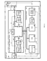
- FIG. 3 illustrates an exemplary combination-type smart card 300 that includes a DIVRS 305 and a processing system 310 .
- the smart card 300 is configured to receive power from either an ISO (International Standard Organization) interface 315 or through an RF interface 320 .
- the DIVRS 305 selects whether to draw operating current from the ISO interface 315 or from the RF interface 320 .
- the current that is drawn may be controlled to supply a substantially constant voltage Vdd at a output node 322 .
- the DIVRS 305 may further perform such selection and regulation operation while substantially reducing or preventing reverse current from flowing from the output node 322 to either of the interfaces 315 , 320 , such as when these interfaces are not actively powered by a power source.
- the DIVRS 305 may receive power from any of a number of different power sources, and power sources may be powered or depowered in various sequences.
- the ISO interface 315 is a physical interface that can receive power through direct electrical contact between conductors connected to a power source, such as a battery or other external DC power supply, for example.
- the RF interface 320 converts RF signals that are coupled to an antenna 325 .
- the RF interface 320 also includes a rectifier 330 and a capacitor circuit 335 .
- the rectifier may rectify energy in the received RF signals for storage in the capacitor circuit 335 .
- received energy may also be stored by charging a battery (not shown) in the smart card 300 .
- transistors 340 , 345 are PMOS transistors.
- the transistor 340 has a source terminal connected to the ISO interface 315 and a drain terminal connected to the output node 322 (Vdd).
- the transistor 345 has a source terminal connected to the RF interface 320 and a drain terminal connected to the output node 322 .
- Each of the transistors 340 , 345 has a gate terminal that can be biased to modulate the resistance between the respective source and drain terminals.
- the DIVRS 305 includes two mode circuits 350 , 355 to supply a gate voltage to the transistors 340 , 345 , respectively.
- the mode circuits 350 , 355 may enable or disable the transistors 340 , 345 , respectively.
- the mode circuits 350 may disable the transistor 340 by raising Vgs substantially higher than Vth.
- the DIVRS 305 also includes two regulator control circuits 360 , 365 and a mode controller 370 . These control circuits 360 , 365 and the controller 370 cooperate to provide signals to control the mode circuits 350 , 355 .
- the regulator control circuits 360 , 365 generate regulated bias signals Vb 1 , Vb 2 to bias the gates of the transistors 340 , 345 , respectively.
- one of the regulator control circuits 360 , 365 can generate a bias signal to regulate the output voltage Vdd at the drain of the corresponding transistor.
- the mode circuits 350 , 355 also receive control signals from the mode controller 370 .
- the mode controller 370 supplies a control signal sel 1 and a disable signal d 2 to the mode circuit 350 , and a control signal sel 2 and a disable signal d 2 to the mode circuit 355 .
- the mode circuit 350 selects to transmit to the gate terminal of the transistor 340 either Vb 1 from the regulator control circuit 360 or d 1 from the mode controller 370 .
- the mode circuit 355 selects to transmit to the gate terminal of the transistor 345 either Vb 2 from the regulator control circuit 365 or d 2 from the mode controller 370 .
- the mode circuit 350 selects to transmit Vb 1 .
- the mode circuit 350 selects to transmit d 1 .
- the mode circuit 355 transmits Vb 2 .
- the mode circuit 355 transmits d 2 .
- the mode controller 370 generates the control signals sel 1 , sel 2 and the disable signal d 1 , d 2 based on measured input voltages V 1 and V 2 .
- the mode controller 370 may generate d 1 , d 2 using the highest available input voltage V 1 , V 2 .
- the mode controller 370 may be configured to supply the highest available input voltage as d 1 , d 2 through a pull-up resistor. In a negative supply, pull-down resistors to the most negative available voltage may be used to generate d 1 , d 2 .
- the mode controller 370 selects an operating mode based on V 1 , V 2 , and then generates sel 1 , sel 2 according to the selected operating mode. In a first operating mode, the mode controller 370 activates the transistor 340 and deactivates the transistor 345 . In a second operating mode, the controller 370 activates the transistor 345 and deactivates the transistor 340 .
- the mode controller 370 selects the first operating mode by asserting sel 1 to enable the transistor 340 and deasserting sel 2 to disable the transistor 345 .
- the mode circuit 355 transmits the disable signal d 2 , which is the highest available input voltage, to the gate of the transistor 345 . Biasing the gate terminal of the transistor 345 with the highest available voltage, in the first operating mode, may substantially reduce or prevent reverse current through the transistor 345 from the output node 322 .
- V 1 is smaller than V 2
- the mode controller 370 selects the second operating mode by asserting sel 2 to enable the transistor 345 and deasserting sel 1 to disable the transistor 340 .
- a reverse current through the transistor 340 from the output node 322 is substantially prevented because the gate terminal of the transistor 340 is pulled-up to the highest available voltage.
- an RF power source is active (e.g., supplying a voltage of 3.8V at V 2 ) while the ISO power is substantially at zero volts.
- the mode controller 370 selects the second operating mode to enable the transistor 345 to supply current to the processing system 310 .
- the gate voltage of the transistor 340 is pulled higher than Vdd.
- the transistor 340 is thus held in a high impedance state by the mode circuit 350 . Accordingly, transistors that are connected to inactive power sources may be effectively protected against reverse current conditions by pulling up the gate of the unselected transistor to the highest available input voltage.
- the mode controller 370 may control the regulator control circuits 360 , 365 such that only one of the transistors 340 , 345 is active and supplying current to the output node 322 . Exemplary implementations of this method are described with reference to FIG. 5 .
- the smart card 300 further includes a processing system 310 that operates from the regulated voltage supplied by the DIVRS 305 .
- the processing system 310 includes a microprocessor 375 , a random access memory (RAM) 380 , a read-only memory (ROM) 385 , and a RF signal modulator/demodulator (modem) 390 for processing data, such as receiving, storing, processing, and/or transmitting information.
- the processing system 310 also includes bus 395 for data communication.
- the microprocessor 375 may execute software and then process data stored in the RAM 380 .
- the ROM 385 may store boot code that the microprocessor 375 executes upon activation of the smart card 300 .
- the microprocessor 375 may also transmit and/or receive data from an external source via the ISO interface 315 (e.g., ISO 7816 contact interface) and/or the RF interface 320 (e.g., ISO 14443 contactless interface).
- the microprocessor 375 may use software stored in the RAM 380 to transmit and receive data according to a predetermined communication protocol used by the ISO interface 315 .
- the microprocessor 375 may also transmit and receive data to/from the RF interface 320 using the RF signal modem 390 .
- the processing system 310 may receive data by modulating a RF signal that also provides power to the smartcard 300 through the rectifier 330 .
- the smart card 300 may also use the RF signal modem 335 to transmit data to a receiving device via the RF interface 320 .
- the processing system 310 also includes a RF clock detector 397 to detect, monitor, and shape a clock signal embedded in a received RF signal.
- the RF clock detector 397 may detect a clock frequency used by an external source. The detected clock frequency may be used to generate a signal that drives a system clock to control, for example, a modem, processor unit, and peripheral circuits.
- data reception may be handled using an analog envelop detector circuit and bandpass filter to demodulate an amplitude modulated (AM) signal.
- Data transmission may be handled by inducing and removing a short circuit across the terminals of the antenna 325 .
- a reader system may be configured to the resulting changes in inductance. Transmitted data may be encoded using, for example, binary phase shift keying.
- the processing system 310 may operate using either the power received from the ISO interface 315 , or the power received from the RF interface 320 .
- FIGS. 4A-4B show exemplary circuits that implement the DIVRS 305 .
- the DIVRS 305 receives independently sourced power inputs from an input node 401 at voltage V 1 and another input node 402 at voltage V 2 .
- the DIVRS 305 may select to enable the transistor 340 and to disable the transistor 345 .
- the DIVRS 305 may select to enable the transistor 345 and to disable the transistor 340 .
- the DIVRS 305 may enable or disable the transistors 340 , 345 using the mode circuits 350 , 355 .
- the mode circuits 350 , 355 are implemented as multiplexers (MUXs).
- the mode circuits 350 , 355 receive control signals sel 1 and sel 2 , respectively, from the mode controller 370 . Using these control signals, the mode circuits 350 , 355 provide a selected input to a gate of the transistors 340 , 345 , respectively, to enable or disable the transistors 340 , 345 .
- Both of the mode circuits 350 , 355 may receive two separate gate bias voltages.
- the mode circuits 350 may receive Vb 1 from the regulator control circuit 360 and d 1 from the mode controller 370 .
- the mode circuit 355 may receive Vb 2 from the regulator control circuit 365 and d 2 from the mode controller 370 . Based on the control signals (sel 1 or sel 2 ), the mode circuits 350 , 355 selects one of the two bias voltages to be transmitted to the transistors 340 , 345 , respectively.
- the mode controller 370 includes a voltage detector 405 , a mode select logic 410 , and a reference select logic 415 .
- the voltage detector 405 is configured to detect whether V 1 at the input node 401 is above a threshold (e.g., 2.3 V, 3.3 V, etc.) and whether V 2 at the input node 402 is above a threshold.
- the voltage detector 405 may generate a signal indicating whether V 1 is greater than the threshold and another signal indicating whether V 2 is greater than the threshold.
- the mode controller 370 may use the generated signal to determine whether the regulator control circuits 360 , 365 are activated.
- the mode select logic 410 receives a signal indicating whether V 1 at the input node 401 is within an acceptable voltage range, a signal indicating whether V 2 at the input node 402 is within an acceptable voltage range, and a signal indicating a preferred voltage supply setting to the input node 401 or the input node 402 . Based on the received signals, the mode select logic 410 selects one of the input node 401 , 402 to be the active voltage supply. When only one of the input voltages V 1 , V 2 are within the acceptable voltage range, the mode select logic 410 may select the input node with the acceptable voltage as the active voltage supply.
- the mode select logic 410 may use the preferred voltage supply signal to determine which of the input nodes 401 , 402 to be the active voltage supply.
- the preferred voltage supply may be set to an input node that supplies the highest voltage.
- the preferred voltage supply may be selected by a manufacturer or by a user.
- the user may set the input node 402 to be the preferred voltage supply.
- the mode select logic 410 may select the input node 402 as the active power supply when V 2 is in the acceptable range, even if V 1 is higher than V 2 .
- Such techniques may be used to provide dual regulation in stand-alone and/or networked systems. Selections may be implemented in a smart card system, for example, by executing code stored in a data store, such as the ROM 385 , or by a signal received at a port (e.g., input/output (I/O)) pin.
- I/O input/output
- FIG. 4B shows an exemplary circuit in which the regulator control circuits 360 , 365 directly generate gate bias signals to the transistors 340 , 345 without passing through a MUX.
- the control signals sel 1 , sel 2 directly enable or disable the regulator control circuits 360 , 365 .
- each of the regulator control circuits 360 , 365 operates to disable its corresponding transistor 340 , 345 .
- An example of operation for the mode select logic 410 is described with reference to FIG. 5 .
- the gate bias voltages Vb 1 , Vb 2 generated by the regulator control circuits 360 , 365 may be controlled by the reference select logic 415 .
- the regulator control circuit 360 receives a reference voltage Vref 2 from a voltage source 430
- the regulator control circuit 365 receives a reference voltage Vref 2 from the voltage source 435 .
- the voltage sources 430 , 435 may be controlled by the reference select logic 415 depending on the present operating mode.
- a reference voltage supplied to the unselected regulator control circuit may be adjusted to be only a fraction of the target regulation voltage level. This may allow the unselected regulator to restore full operating voltage more quickly when the selected regulator fails to maintain regulation of the output voltage at the target regulation voltage.
- the reference select logic 415 may select a higher reference voltage (e.g., 1.6 V) for the regulator control circuit 360 and a lower reference voltage (e.g., 1.4 V) for the regulator control circuit 365 .
- the reference select logic 415 may select a higher reference voltage for the regulator control circuit 365 and a lower reference voltage for the regulator control circuit 360 .
- FIG. 5 shows a flow chart that illustrates an exemplary method 500 of operations for substantially preventing reverse current through an inactive regulator.
- the method 500 includes operations that may be performed generally by a mode controller (e.g., the mode controller 370 ).
- the operations may be performed under the control, supervision, and/or monitoring of a mode selection logic (e.g., the mode select logic 410 ) and a reference select logic (e.g., the reference select logic 415 ).
- Operations may also be supplemented or augmented by other processing and/or control elements that may be incorporated by other elements coupled to the mode controller.
- the processing may be implemented using analog and/or digital hardware or techniques, either alone or in cooperation with one or more processors executing instructions.
- the method 500 begins at step 505 when a check of the supply voltages, V 1 , V 2 is made, examples of which are described with reference to FIG. 3 .
- a determination is made, at step 510 , whether there is an inactive voltage.
- the mode controller 370 may use the voltage detector 405 to detect whether any of the input nodes are not coupled to an active power source.
- the mode controller may check a signal generated by the voltage detector 405 . If V 1 is inactive, then, at step 520 , a bias signal may be applied using V 2 to disable a voltage regulator that is connected to V 1 .
- the reference select logic 415 may select a target reference voltage for the regulator connected to V 2 and disable the regulator connected to V 1 by applying a sufficiently high gate voltage.
- a bias signal is applied using V 1 to disable a voltage regulator that is connected to V 2 .
- the reference select logic 415 may select a target reference voltage for the regulator connected to V 1 and disable the regulator connected to V 2 by applying a sufficiently high gate voltage.
- the step 525 is repeated.
- step 510 If, at step 510 , there is no inactive voltage, then a comparison is made between the voltage at V 1 and V 2 at step 535 . If the voltage at V 1 is greater than the voltage at V 2 , then the reference voltage for the regulator of V 1 is selected to be Vdd at step 540 and the reference voltage for the regulator of V 2 is set to be Vdd less an offset at step 545 . For example, if the Vdd is set to 1.6 V and the offset is set to 0.2 V, then the reference voltage for the regulator of V 1 is 1.6 V and the reference voltage for the regulator of V 2 is 1.4 V. After the reference voltages are configured, then the step 525 is repeated.
- step 535 the voltage at V 2 is greater than the voltage at V 1 . If, at step 535 , the voltage at V 2 is greater than the voltage at V 1 , then, at step 550 , the reference voltage for the regulator of V 2 I selected to be Vdd and, at step 555 , the reference voltage for the regulator of V 1 is selected to be Vdd less an offset. After the reference voltages are set, the step 525 is repeated.
- the mode controller 370 may be configured to generate mode control signals for selecting an active voltage regulator between more than two voltage regulators.
- a DIVRS may include more than two voltage inputs, such as three or more voltage inputs.
- a voltage regulator associated with each input may be controlled by a mode circuit responsive to a mode control signal.
- the mode controller may, for example, monitor each voltage input signal, determine the highest available voltage, and generate mode control signals to each mode circuit to substantially prevent current from flowing from the highest available voltage to the other voltage inputs through their corresponding voltage regulator circuits.
- the mode controller can generate control signals to cause multiple voltage regulators to be disabled based on information about the input voltages.
- current regulators may be used.
- detector circuitry monitors both the voltage and the current flowing through shunts of the current regulators.
- the pass transistors initially are both off.
- the supply voltages (V 1 or V 2 ) being activated, the voltage on the source side of the PMOS transistor rises.
- the regulator's current shunt stage may be turned on. Once sufficient current is running through the shunt, the regulator's pass transistor may be turned on.
- the DIVRS 100 or the DIVRS 305 may include additional logic to provide mode control for using voltage supplies that are negative with respect to a circuit reference voltage (e.g., ground).
- a circuit reference voltage e.g., ground
- the DIVRS 305 may use N-channel MOS for such negative voltages.
- the mode controller 370 may disable voltage regulators by pulling the MOS gate voltage substantially toward the most negative available input supply voltage.
- the mode selection by the mode controller 106 or the mode controller 370 may be based on one or more factors, taken alone or in combination.
- factors may include, any or all of hysteresis, filtering, or providing a default mode value, voltage thresholds, and/or a time delay.
- the mode controller 370 may implement hysteresis to reduce undesirable mode switching. For example, when V 1 is substantially close to V 2 , the mode controller 370 may not change operating mode even when the present active voltage is slightly less than the unselected voltage.
- the mode controller 370 or the mode controller 106 may also read a default mode value to select the operating mode.
- the default-mode value may be preset by, for example, a user or a manufacturer.
- the manufacturer may select a default mode value to be the RF power supply.
- the mode controller 370 may select the RF power supply to be the active power supply. In various implementations, this may involve the microprocessor 375 executing instructions (e.g., boot code) stored in a data store, such as the ROM 385 , for example.
- the mode controller 106 or the mode controller 370 may include different voltage thresholds for V 1 and V 2 .
- the mode controller 370 may require different minimum active levels for each of the power supplies V 1 and V 2 .
- the mode controller 370 may require the V 1 to be at least 1.5 V to be considered active but the mode controller 370 may require the V 2 to be at least 2.3 V to be considered active.
- the mode controller 106 or the mode controller 370 may include, for example, a filter and/or a digital delay before switching operating mode to avoid mode switching due to noise or transient voltages.
- the filter may actively and/or passively low pass filter, for example, voltages at one or more input nodes. Filtering may be supplemented with digital signal processing.
- the smart card 300 may temporarily receive a spike of voltage at the RF interface 320 when, for example, a computer is turned on near the smart card 300 . If the mode controller 370 includes an resistor-capacitor (RC) network and/or a time delay before switching operating mode, the smart card 300 may continue to be supplied by the V 1 without changing to the V 2 and back. This may improve stability and reduce noise on the current supplied to the processing system 310 .
- RC resistor-capacitor
- bipolar junction transistors instead of PMOS may be used.
- a mode controller may be implemented to control a base voltage of a BJT to enable and disable a voltage regulator. By doing so, a reverse current may be substantially prevented through the disabled BJT.
- caching e.g., L1, L2, etc. . . .
- Random access memory may be included, for example, to provide scratch pad memory and or to load executable code or parameter information stored for use during runtime operations.
- Other hardware and software may be provided to perform operations, such as network or other communications using one or more protocols, wireless (e.g., infrared) communications, stored operational energy and power supplies (e.g., batteries), switching and/or linear power supply circuits, software maintenance (e.g., self-test, upgrades).
- One or more communication interfaces may be provided in support of data storage and related operations.
- Some systems may be implemented as a computer system that can be used with implementations of the invention.
- various implementations may include digital and/or analog circuitry, computer hardware, firmware, software, or combinations thereof.
- Apparatus can be implemented in a computer program product tangibly embodied in an information carrier, e.g., in a machine-readable storage device or in a propagated signal, for execution by a programmable processor; and methods can be performed by a programmable processor executing a program of instructions to perform functions of the invention by operating on input data and generating an output.
- the invention can be implemented advantageously in one or more computer programs that are executable on a programmable system including at least one programmable processor coupled to receive data and instructions from, and to transmit data and instructions to, a data storage system, at least one input device, and/or at least one output device.
- a computer program is a set of instructions that can be used, directly or indirectly, in a computer to perform a certain activity or bring about a certain result.
- a computer program can be written in any form of programming language, including compiled or interpreted languages, and it can be deployed in any form, including as a stand-alone program or as a module, component, subroutine, or other unit suitable for use in a computing environment.
- Suitable processors for the execution of a program of instructions include, by way of example, both general and special purpose microprocessors, which may include a single processor or one of multiple processors of any kind of computer.
- a processor will receive instructions and data from a read-only memory or a random access memory or both.
- the essential elements of a computer are a processor for executing instructions and one or more memories for storing instructions and data.
- a computer will also include, or be operatively coupled to communicate with, one or more mass storage devices for storing data files; such devices include magnetic disks, such as internal hard disks and removable disks; magneto-optical disks; and optical disks.
- Storage devices suitable for tangibly embodying computer program instructions and data include all forms of non-volatile memory, including, by way of example, semiconductor memory devices, such as EPROM, EEPROM, and flash memory devices; magnetic disks, such as internal hard disks and removable disks; magneto-optical disks; and, CD-ROM and DVD-ROM disks.
- semiconductor memory devices such as EPROM, EEPROM, and flash memory devices
- magnetic disks such as internal hard disks and removable disks
- magneto-optical disks and, CD-ROM and DVD-ROM disks.
- the processor and the memory can be supplemented by, or incorporated in, ASICs (application-specific integrated circuits).
- ASICs application-specific integrated circuits
- each system 100 may be programmed with the same or similar information and/or initialized with substantially identical information stored in volatile and/or non-volatile memory.
- one data interface may be configured to perform auto configuration, auto download, and/or auto update functions when coupled to an appropriate host device, such as a desktop computer or a server.
Abstract
Description
Claims (23)
Priority Applications (5)
| Application Number | Priority Date | Filing Date | Title |
|---|---|---|---|
| US11/538,613 US8013473B2 (en) | 2006-09-01 | 2006-10-04 | Detector based combination regulator |
| PCT/US2007/077391 WO2008028132A2 (en) | 2006-09-01 | 2007-08-31 | Detector based combination regulator |
| DE200711002047 DE112007002047T5 (en) | 2006-09-01 | 2007-08-31 | Detector-based combination controller |
| CN2007800319829A CN101512863B (en) | 2006-09-01 | 2007-08-31 | Detector based combination regulator |
| TW96132662A TWI464686B (en) | 2006-09-01 | 2007-08-31 | Voltage regulatiion system |
Applications Claiming Priority (2)
| Application Number | Priority Date | Filing Date | Title |
|---|---|---|---|
| US84184706P | 2006-09-01 | 2006-09-01 | |
| US11/538,613 US8013473B2 (en) | 2006-09-01 | 2006-10-04 | Detector based combination regulator |
Publications (2)
| Publication Number | Publication Date |
|---|---|
| US20080054721A1 US20080054721A1 (en) | 2008-03-06 |
| US8013473B2 true US8013473B2 (en) | 2011-09-06 |
Family
ID=39136946
Family Applications (1)
| Application Number | Title | Priority Date | Filing Date |
|---|---|---|---|
| US11/538,613 Expired - Fee Related US8013473B2 (en) | 2006-09-01 | 2006-10-04 | Detector based combination regulator |
Country Status (5)
| Country | Link |
|---|---|
| US (1) | US8013473B2 (en) |
| CN (1) | CN101512863B (en) |
| DE (1) | DE112007002047T5 (en) |
| TW (1) | TWI464686B (en) |
| WO (1) | WO2008028132A2 (en) |
Cited By (5)
| Publication number | Priority date | Publication date | Assignee | Title |
|---|---|---|---|---|
| US20120318875A1 (en) * | 2011-06-14 | 2012-12-20 | Jong-Pil Cho | Internal voltage generating circuit and smart card |
| US20150194886A1 (en) * | 2014-01-08 | 2015-07-09 | Pedro Barbosa Zanetta | Voltage regulation system for integrated circuit |
| US11188109B1 (en) * | 2020-08-10 | 2021-11-30 | SK Hynix Inc. | Devices configured to conduct a power gating operation |
| US20220407503A1 (en) * | 2021-06-17 | 2022-12-22 | Nxp B.V. | Mode detector for dc-dc converters |
| US11694050B2 (en) | 2020-07-09 | 2023-07-04 | Samsung Electronics Co., Ltd. | Internal voltage generator and smart card including the same |
Families Citing this family (20)
| Publication number | Priority date | Publication date | Assignee | Title |
|---|---|---|---|---|
| US8401219B2 (en) | 2007-01-05 | 2013-03-19 | Apple Inc. | Headset connector |
| JP4786316B2 (en) * | 2005-12-05 | 2011-10-05 | ルネサスエレクトロニクス株式会社 | Semiconductor integrated circuit device and IC card using the same |
| US8712071B2 (en) * | 2007-01-05 | 2014-04-29 | Apple Inc. | Headset electronics |
| US9118990B2 (en) | 2007-01-06 | 2015-08-25 | Apple Inc. | Connectors designed for ease of use |
| EP2654270B8 (en) | 2007-01-06 | 2018-04-11 | Apple Inc. | Wireless headset comprising a housing and an earbud electrically coupled to the housing by a flexible circuit board |
| DK2654270T3 (en) * | 2007-01-06 | 2017-12-04 | Apple Inc | WIRELESS HEADS CONTAINING A HOUSE AND A EARBLE ELECTRIC CONNECTED TO THE HOUSE THROUGH A FLEXIBLE CIRCUIT PLATE |
| KR100900476B1 (en) * | 2007-02-16 | 2009-06-03 | 삼성전자주식회사 | Mobile communication device and battery recharge method thereof |
| US8364989B2 (en) * | 2007-09-26 | 2013-01-29 | Infineon Technologies Ag | Power supply input selection circuit |
| DE102008027392B4 (en) * | 2008-06-09 | 2019-03-21 | Atmel Corp. | Circuit and method for operating a circuit |
| JP6032900B2 (en) * | 2012-02-06 | 2016-11-30 | キヤノン株式会社 | Electronics |
| US9621213B2 (en) | 2015-03-31 | 2017-04-11 | Paypal, Inc. | Smart card battery charging during card use |
| US10582284B2 (en) | 2015-09-30 | 2020-03-03 | Apple Inc. | In-ear headphone |
| EP3208748B1 (en) | 2016-02-19 | 2019-06-12 | Nxp B.V. | Power switching circuit |
| CN107919653B (en) * | 2016-10-10 | 2022-01-11 | 恩智浦有限公司 | Reverse current protection circuit for switching circuit |
| TWI604372B (en) * | 2016-11-14 | 2017-11-01 | 瑞昱半導體股份有限公司 | Intermediate circuit for memory card access |
| CN108090548A (en) * | 2016-11-21 | 2018-05-29 | 瑞昱半导体股份有限公司 | For the intermediary circuit of storage card access |
| US10866606B2 (en) * | 2018-03-28 | 2020-12-15 | Qualcomm Incorporated | Methods and apparatuses for multiple-mode low drop out regulators |
| CN110504741A (en) * | 2018-09-14 | 2019-11-26 | 深圳市文鼎创数据科技有限公司 | A kind of power supply switch circuit of smart card and smart card |
| US11482889B2 (en) | 2019-01-09 | 2022-10-25 | Integrated Device Technology, Inc. | Wireless power receiver configurable for LDO or buck operation |
| EP4235500A1 (en) * | 2022-02-25 | 2023-08-30 | STMicroelectronics razvoj polprevodnikov d.o.o. | Ic card regulator |
Citations (32)
| Publication number | Priority date | Publication date | Assignee | Title |
|---|---|---|---|---|
| US4617473A (en) * | 1984-01-03 | 1986-10-14 | Intersil, Inc. | CMOS backup power switching circuit |
| US5206495A (en) | 1989-10-24 | 1993-04-27 | Angewandte Digital Elektronik Gmbh | Chip card |
| US5555182A (en) * | 1995-05-04 | 1996-09-10 | Cyberex, Inc. | Source quality monitoring system |
| EP0736828A2 (en) | 1995-04-06 | 1996-10-09 | Seiko Epson Corporation | Battery driven electronic apparatus and method of controlling power supply in the apparatus |
| WO1997049059A1 (en) * | 1996-06-19 | 1997-12-24 | Inside Technologies | Device for stabilising a microcircuit supply voltage |
| US5777903A (en) * | 1996-01-22 | 1998-07-07 | Motorola, Inc. | Solar cell powered smart card with integrated display and interface keypad |
| US5845217A (en) | 1993-09-15 | 1998-12-01 | Ericsson Inc. | Power systems for plug-in modules |
| US5889431A (en) | 1997-06-26 | 1999-03-30 | The Aerospace Corporation | Current mode transistor circuit method |
| US5929416A (en) * | 1994-11-28 | 1999-07-27 | Telecomunicacoes Brasileiras S/A - Telebras | Reading head arrangement for two data card types |
| US5973484A (en) | 1997-05-07 | 1999-10-26 | Lg Semicon Co., Ltd. | Voltage regulator circuit for semiconductor memory device |
| US6003777A (en) * | 1996-08-05 | 1999-12-21 | Inside Technologies | Microcircuit chip card with contact and contactless operating modes |
| WO2000058815A1 (en) | 1999-03-30 | 2000-10-05 | Qlogic Corporation | Add-on card with automatic bus power line selection circuit |
| US6150803A (en) | 2000-03-28 | 2000-11-21 | Linear Technology Corporation | Dual input, single output power supply |
| US6177783B1 (en) | 1999-09-13 | 2001-01-23 | Adc Telecommunications, Inc. | Current balancing for voltage regulator having inputs from multiple power supplies |
| US6225708B1 (en) | 1998-06-05 | 2001-05-01 | International Business Machine Corporation | Uninterruptable power supply |
| US6566935B1 (en) * | 1999-08-31 | 2003-05-20 | Stmicroelectronics S.A. | Power supply circuit with a voltage selector |
| US6642631B1 (en) | 2000-10-17 | 2003-11-04 | Semiconductor Components Industries Llc | Circuit and method of direct duty cycle current sharing |
| US6724588B1 (en) | 1999-09-22 | 2004-04-20 | Dell Usa L.P. | Power supply selector |
| US20040210406A1 (en) | 2003-04-18 | 2004-10-21 | Dell Products L.P. | Information handling system including a power management apparatus capable of independently switching between a primary and secondary battery |
| US20050046461A1 (en) | 2003-08-26 | 2005-03-03 | Texas Instruments Incorporated | Cross-conduction blocked power selection comparison/control circuitry with NTC (negative temperature coefficient) trip voltage |
| CN1637780A (en) | 2003-09-05 | 2005-07-13 | 三星电子株式会社 | Chip card with simultaneous contact and contact-less operations |
| US20050150488A1 (en) | 2002-02-22 | 2005-07-14 | Dave Rajiv B. | Dose dispensing system and apparatus |
| US6933772B1 (en) | 2004-02-02 | 2005-08-23 | Freescale Semiconductor, Inc. | Voltage regulator with improved load regulation using adaptive biasing |
| US6979983B2 (en) | 2004-04-28 | 2005-12-27 | Faraday Technology Corp. | Voltage regulator |
| US20060017423A1 (en) | 2004-07-26 | 2006-01-26 | Frith Peter J | Dual power bus for battery powered device |
| US20060022640A1 (en) | 2004-07-26 | 2006-02-02 | Peter Frith | Power supply circuit for portable battery powered device |
| US7109691B2 (en) | 2002-06-28 | 2006-09-19 | Microsemi Corporation | Systems for auto-interleaving synchronization in a multiphase switching power converter |
| EP1713185A1 (en) * | 2004-02-02 | 2006-10-18 | Fujitsu Frontech Limited | Ic card reading apparatus and reading method thereof |
| US7246750B2 (en) * | 2003-09-05 | 2007-07-24 | Samsung Electronics Co., Ltd. | Chip card with simultaneous contact and contact-less operations |
| US7332896B2 (en) | 2004-12-28 | 2008-02-19 | Samsung Electronics Co., Ltd. | Apparatus and method for controlling supply voltage in multiple interface card |
| US20080084195A1 (en) * | 2006-10-04 | 2008-04-10 | Louis Frew | Analog Combination Regulator |
| US7554383B2 (en) | 2001-03-02 | 2009-06-30 | Sony Corporation | Chip for non-contact reader/writer having power-supply management function |
Family Cites Families (1)
| Publication number | Priority date | Publication date | Assignee | Title |
|---|---|---|---|---|
| US7212414B2 (en) * | 1999-06-21 | 2007-05-01 | Access Business Group International, Llc | Adaptive inductive power supply |
-
2006
- 2006-10-04 US US11/538,613 patent/US8013473B2/en not_active Expired - Fee Related
-
2007
- 2007-08-31 CN CN2007800319829A patent/CN101512863B/en not_active Expired - Fee Related
- 2007-08-31 WO PCT/US2007/077391 patent/WO2008028132A2/en active Application Filing
- 2007-08-31 DE DE200711002047 patent/DE112007002047T5/en not_active Withdrawn
- 2007-08-31 TW TW96132662A patent/TWI464686B/en not_active IP Right Cessation
Patent Citations (32)
| Publication number | Priority date | Publication date | Assignee | Title |
|---|---|---|---|---|
| US4617473A (en) * | 1984-01-03 | 1986-10-14 | Intersil, Inc. | CMOS backup power switching circuit |
| US5206495A (en) | 1989-10-24 | 1993-04-27 | Angewandte Digital Elektronik Gmbh | Chip card |
| US5845217A (en) | 1993-09-15 | 1998-12-01 | Ericsson Inc. | Power systems for plug-in modules |
| US5929416A (en) * | 1994-11-28 | 1999-07-27 | Telecomunicacoes Brasileiras S/A - Telebras | Reading head arrangement for two data card types |
| EP0736828A2 (en) | 1995-04-06 | 1996-10-09 | Seiko Epson Corporation | Battery driven electronic apparatus and method of controlling power supply in the apparatus |
| US5555182A (en) * | 1995-05-04 | 1996-09-10 | Cyberex, Inc. | Source quality monitoring system |
| US5777903A (en) * | 1996-01-22 | 1998-07-07 | Motorola, Inc. | Solar cell powered smart card with integrated display and interface keypad |
| WO1997049059A1 (en) * | 1996-06-19 | 1997-12-24 | Inside Technologies | Device for stabilising a microcircuit supply voltage |
| US6003777A (en) * | 1996-08-05 | 1999-12-21 | Inside Technologies | Microcircuit chip card with contact and contactless operating modes |
| US5973484A (en) | 1997-05-07 | 1999-10-26 | Lg Semicon Co., Ltd. | Voltage regulator circuit for semiconductor memory device |
| US5889431A (en) | 1997-06-26 | 1999-03-30 | The Aerospace Corporation | Current mode transistor circuit method |
| US6225708B1 (en) | 1998-06-05 | 2001-05-01 | International Business Machine Corporation | Uninterruptable power supply |
| WO2000058815A1 (en) | 1999-03-30 | 2000-10-05 | Qlogic Corporation | Add-on card with automatic bus power line selection circuit |
| US6566935B1 (en) * | 1999-08-31 | 2003-05-20 | Stmicroelectronics S.A. | Power supply circuit with a voltage selector |
| US6177783B1 (en) | 1999-09-13 | 2001-01-23 | Adc Telecommunications, Inc. | Current balancing for voltage regulator having inputs from multiple power supplies |
| US6724588B1 (en) | 1999-09-22 | 2004-04-20 | Dell Usa L.P. | Power supply selector |
| US6150803A (en) | 2000-03-28 | 2000-11-21 | Linear Technology Corporation | Dual input, single output power supply |
| US6642631B1 (en) | 2000-10-17 | 2003-11-04 | Semiconductor Components Industries Llc | Circuit and method of direct duty cycle current sharing |
| US7554383B2 (en) | 2001-03-02 | 2009-06-30 | Sony Corporation | Chip for non-contact reader/writer having power-supply management function |
| US20050150488A1 (en) | 2002-02-22 | 2005-07-14 | Dave Rajiv B. | Dose dispensing system and apparatus |
| US7109691B2 (en) | 2002-06-28 | 2006-09-19 | Microsemi Corporation | Systems for auto-interleaving synchronization in a multiphase switching power converter |
| US20040210406A1 (en) | 2003-04-18 | 2004-10-21 | Dell Products L.P. | Information handling system including a power management apparatus capable of independently switching between a primary and secondary battery |
| US20050046461A1 (en) | 2003-08-26 | 2005-03-03 | Texas Instruments Incorporated | Cross-conduction blocked power selection comparison/control circuitry with NTC (negative temperature coefficient) trip voltage |
| CN1637780A (en) | 2003-09-05 | 2005-07-13 | 三星电子株式会社 | Chip card with simultaneous contact and contact-less operations |
| US7246750B2 (en) * | 2003-09-05 | 2007-07-24 | Samsung Electronics Co., Ltd. | Chip card with simultaneous contact and contact-less operations |
| EP1713185A1 (en) * | 2004-02-02 | 2006-10-18 | Fujitsu Frontech Limited | Ic card reading apparatus and reading method thereof |
| US6933772B1 (en) | 2004-02-02 | 2005-08-23 | Freescale Semiconductor, Inc. | Voltage regulator with improved load regulation using adaptive biasing |
| US6979983B2 (en) | 2004-04-28 | 2005-12-27 | Faraday Technology Corp. | Voltage regulator |
| US20060022640A1 (en) | 2004-07-26 | 2006-02-02 | Peter Frith | Power supply circuit for portable battery powered device |
| US20060017423A1 (en) | 2004-07-26 | 2006-01-26 | Frith Peter J | Dual power bus for battery powered device |
| US7332896B2 (en) | 2004-12-28 | 2008-02-19 | Samsung Electronics Co., Ltd. | Apparatus and method for controlling supply voltage in multiple interface card |
| US20080084195A1 (en) * | 2006-10-04 | 2008-04-10 | Louis Frew | Analog Combination Regulator |
Non-Patent Citations (2)
| Title |
|---|
| ATMEL Corporation, International Search Report and the Written Opinion of the corresponding PCT application No. PCT/US2007/077391 dated Apr. 28, 2008, 10 pages. |
| Ayers, John E., "Digital Integrated Circuits Analysis and Design", USPTO Aug. 17, 2004, CRC Press, pp. 261-264. |
Cited By (8)
| Publication number | Priority date | Publication date | Assignee | Title |
|---|---|---|---|---|
| US20120318875A1 (en) * | 2011-06-14 | 2012-12-20 | Jong-Pil Cho | Internal voltage generating circuit and smart card |
| US8944334B2 (en) * | 2011-06-14 | 2015-02-03 | Samsung Electronics Co., Ltd. | Internal voltage generating circuit and smart card |
| US20150194886A1 (en) * | 2014-01-08 | 2015-07-09 | Pedro Barbosa Zanetta | Voltage regulation system for integrated circuit |
| US9148056B2 (en) * | 2014-01-08 | 2015-09-29 | Freescale Semiconductor, Inc. | Voltage regulation system for integrated circuit |
| US11694050B2 (en) | 2020-07-09 | 2023-07-04 | Samsung Electronics Co., Ltd. | Internal voltage generator and smart card including the same |
| US11188109B1 (en) * | 2020-08-10 | 2021-11-30 | SK Hynix Inc. | Devices configured to conduct a power gating operation |
| US20220407503A1 (en) * | 2021-06-17 | 2022-12-22 | Nxp B.V. | Mode detector for dc-dc converters |
| US11539351B1 (en) * | 2021-06-17 | 2022-12-27 | Nxp B.V. | Mode detector for DC-DC converters |
Also Published As
| Publication number | Publication date |
|---|---|
| WO2008028132A2 (en) | 2008-03-06 |
| CN101512863A (en) | 2009-08-19 |
| TW200820092A (en) | 2008-05-01 |
| TWI464686B (en) | 2014-12-11 |
| DE112007002047T5 (en) | 2009-07-23 |
| CN101512863B (en) | 2012-08-08 |
| WO2008028132A3 (en) | 2008-08-07 |
| US20080054721A1 (en) | 2008-03-06 |
Similar Documents
| Publication | Publication Date | Title |
|---|---|---|
| US8013473B2 (en) | Detector based combination regulator | |
| EP2225833B1 (en) | Near field rf communicators | |
| EP2235839B1 (en) | Near field rf communicators | |
| US8729960B2 (en) | Dynamic adjusting RFID demodulation circuit | |
| US9661444B2 (en) | Regulation and load modulation in a near field communication device | |
| US8841890B2 (en) | Shunt regulator circuit having a split output | |
| KR20140068768A (en) | Semiconductor integrated circuit and operation method of the same | |
| KR19990082448A (en) | Data exchange system by contact or non-contact communication between terminal and portable device | |
| US8823267B2 (en) | Bandgap ready circuit | |
| US8729874B2 (en) | Generation of voltage supply for low power digital circuit operation | |
| US8669801B2 (en) | Analog delay cells for the power supply of an RFID tag | |
| US8981741B2 (en) | Voltage regulator for contact-less electronic devices | |
| JP3871667B2 (en) | Non-contact IC card | |
| US20120312881A1 (en) | Dynamic power clamp for rfid power control | |
| US9182771B2 (en) | Voltage regulation of near field communication communicators | |
| CN111913552A (en) | Power management for data storage devices | |
| US8584959B2 (en) | Power-on sequencing for an RFID tag | |
| US20080244279A1 (en) | Methods and Apparatus to Detect Voltage Class of a Circuit | |
| US10749365B2 (en) | Power supply method and electronic card using the same | |
| EP2860667B1 (en) | Radio frequency system and method for limiting a voltage | |
| JP2019515404A (en) | Radio frequency identification (RFID) tag and method of limiting power supply voltage of RFID tag |
Legal Events
| Date | Code | Title | Description |
|---|---|---|---|
| AS | Assignment |
Owner name: ATMEL CORPORATION, CALIFORNIA Free format text: ASSIGNMENT OF ASSIGNORS INTEREST;ASSIGNORS:FREW, LOUIS;BATES, COLIN;REEL/FRAME:018358/0340 Effective date: 20061003 |
|
| STCF | Information on status: patent grant |
Free format text: PATENTED CASE |
|
| AS | Assignment |
Owner name: MORGAN STANLEY SENIOR FUNDING, INC. AS ADMINISTRATIVE AGENT, NEW YORK Free format text: PATENT SECURITY AGREEMENT;ASSIGNOR:ATMEL CORPORATION;REEL/FRAME:031912/0173 Effective date: 20131206 Owner name: MORGAN STANLEY SENIOR FUNDING, INC. AS ADMINISTRAT Free format text: PATENT SECURITY AGREEMENT;ASSIGNOR:ATMEL CORPORATION;REEL/FRAME:031912/0173 Effective date: 20131206 |
|
| FPAY | Fee payment |
Year of fee payment: 4 |
|
| AS | Assignment |
Owner name: ATMEL CORPORATION, CALIFORNIA Free format text: TERMINATION AND RELEASE OF SECURITY INTEREST IN PATENT COLLATERAL;ASSIGNOR:MORGAN STANLEY SENIOR FUNDING, INC.;REEL/FRAME:038376/0001 Effective date: 20160404 |
|
| AS | Assignment |
Owner name: JPMORGAN CHASE BANK, N.A., AS ADMINISTRATIVE AGENT, ILLINOIS Free format text: SECURITY INTEREST;ASSIGNOR:ATMEL CORPORATION;REEL/FRAME:041715/0747 Effective date: 20170208 Owner name: JPMORGAN CHASE BANK, N.A., AS ADMINISTRATIVE AGENT Free format text: SECURITY INTEREST;ASSIGNOR:ATMEL CORPORATION;REEL/FRAME:041715/0747 Effective date: 20170208 |
|
| AS | Assignment |
Owner name: JPMORGAN CHASE BANK, N.A., AS ADMINISTRATIVE AGENT, ILLINOIS Free format text: SECURITY INTEREST;ASSIGNORS:MICROCHIP TECHNOLOGY INCORPORATED;SILICON STORAGE TECHNOLOGY, INC.;ATMEL CORPORATION;AND OTHERS;REEL/FRAME:046426/0001 Effective date: 20180529 Owner name: JPMORGAN CHASE BANK, N.A., AS ADMINISTRATIVE AGENT Free format text: SECURITY INTEREST;ASSIGNORS:MICROCHIP TECHNOLOGY INCORPORATED;SILICON STORAGE TECHNOLOGY, INC.;ATMEL CORPORATION;AND OTHERS;REEL/FRAME:046426/0001 Effective date: 20180529 |
|
| AS | Assignment |
Owner name: WELLS FARGO BANK, NATIONAL ASSOCIATION, AS NOTES COLLATERAL AGENT, CALIFORNIA Free format text: SECURITY INTEREST;ASSIGNORS:MICROCHIP TECHNOLOGY INCORPORATED;SILICON STORAGE TECHNOLOGY, INC.;ATMEL CORPORATION;AND OTHERS;REEL/FRAME:047103/0206 Effective date: 20180914 Owner name: WELLS FARGO BANK, NATIONAL ASSOCIATION, AS NOTES C Free format text: SECURITY INTEREST;ASSIGNORS:MICROCHIP TECHNOLOGY INCORPORATED;SILICON STORAGE TECHNOLOGY, INC.;ATMEL CORPORATION;AND OTHERS;REEL/FRAME:047103/0206 Effective date: 20180914 |
|
| FEPP | Fee payment procedure |
Free format text: MAINTENANCE FEE REMINDER MAILED (ORIGINAL EVENT CODE: REM.); ENTITY STATUS OF PATENT OWNER: LARGE ENTITY |
|
| LAPS | Lapse for failure to pay maintenance fees |
Free format text: PATENT EXPIRED FOR FAILURE TO PAY MAINTENANCE FEES (ORIGINAL EVENT CODE: EXP.); ENTITY STATUS OF PATENT OWNER: LARGE ENTITY |
|
| STCH | Information on status: patent discontinuation |
Free format text: PATENT EXPIRED DUE TO NONPAYMENT OF MAINTENANCE FEES UNDER 37 CFR 1.362 |
|
| FP | Lapsed due to failure to pay maintenance fee |
Effective date: 20190906 |
|
| AS | Assignment |
Owner name: MICROSEMI STORAGE SOLUTIONS, INC., ARIZONA Free format text: RELEASE BY SECURED PARTY;ASSIGNOR:JPMORGAN CHASE BANK, N.A., AS ADMINISTRATIVE AGENT;REEL/FRAME:059333/0222 Effective date: 20220218 Owner name: MICROSEMI CORPORATION, ARIZONA Free format text: RELEASE BY SECURED PARTY;ASSIGNOR:JPMORGAN CHASE BANK, N.A., AS ADMINISTRATIVE AGENT;REEL/FRAME:059333/0222 Effective date: 20220218 Owner name: ATMEL CORPORATION, ARIZONA Free format text: RELEASE BY SECURED PARTY;ASSIGNOR:JPMORGAN CHASE BANK, N.A., AS ADMINISTRATIVE AGENT;REEL/FRAME:059333/0222 Effective date: 20220218 Owner name: SILICON STORAGE TECHNOLOGY, INC., ARIZONA Free format text: RELEASE BY SECURED PARTY;ASSIGNOR:JPMORGAN CHASE BANK, N.A., AS ADMINISTRATIVE AGENT;REEL/FRAME:059333/0222 Effective date: 20220218 Owner name: MICROCHIP TECHNOLOGY INCORPORATED, ARIZONA Free format text: RELEASE BY SECURED PARTY;ASSIGNOR:JPMORGAN CHASE BANK, N.A., AS ADMINISTRATIVE AGENT;REEL/FRAME:059333/0222 Effective date: 20220218 |
|
| AS | Assignment |
Owner name: ATMEL CORPORATION, ARIZONA Free format text: RELEASE BY SECURED PARTY;ASSIGNOR:JPMORGAN CHASE BANK, N.A., AS ADMINISTRATIVE AGENT;REEL/FRAME:059262/0105 Effective date: 20220218 |
|
| AS | Assignment |
Owner name: MICROSEMI STORAGE SOLUTIONS, INC., ARIZONA Free format text: RELEASE BY SECURED PARTY;ASSIGNOR:WELLS FARGO BANK, NATIONAL ASSOCIATION, AS NOTES COLLATERAL AGENT;REEL/FRAME:059358/0001 Effective date: 20220228 Owner name: MICROSEMI CORPORATION, ARIZONA Free format text: RELEASE BY SECURED PARTY;ASSIGNOR:WELLS FARGO BANK, NATIONAL ASSOCIATION, AS NOTES COLLATERAL AGENT;REEL/FRAME:059358/0001 Effective date: 20220228 Owner name: ATMEL CORPORATION, ARIZONA Free format text: RELEASE BY SECURED PARTY;ASSIGNOR:WELLS FARGO BANK, NATIONAL ASSOCIATION, AS NOTES COLLATERAL AGENT;REEL/FRAME:059358/0001 Effective date: 20220228 Owner name: SILICON STORAGE TECHNOLOGY, INC., ARIZONA Free format text: RELEASE BY SECURED PARTY;ASSIGNOR:WELLS FARGO BANK, NATIONAL ASSOCIATION, AS NOTES COLLATERAL AGENT;REEL/FRAME:059358/0001 Effective date: 20220228 Owner name: MICROCHIP TECHNOLOGY INCORPORATED, ARIZONA Free format text: RELEASE BY SECURED PARTY;ASSIGNOR:WELLS FARGO BANK, NATIONAL ASSOCIATION, AS NOTES COLLATERAL AGENT;REEL/FRAME:059358/0001 Effective date: 20220228 |