US8008095B2 - Methods for fabricating contacts to pillar structures in integrated circuits - Google Patents
Methods for fabricating contacts to pillar structures in integrated circuits Download PDFInfo
- Publication number
- US8008095B2 US8008095B2 US11/866,455 US86645507A US8008095B2 US 8008095 B2 US8008095 B2 US 8008095B2 US 86645507 A US86645507 A US 86645507A US 8008095 B2 US8008095 B2 US 8008095B2
- Authority
- US
- United States
- Prior art keywords
- hard mask
- pillar structure
- cap
- layer
- liner
- Prior art date
- Legal status (The legal status is an assumption and is not a legal conclusion. Google has not performed a legal analysis and makes no representation as to the accuracy of the status listed.)
- Expired - Fee Related, expires
Links
Images


Classifications
-
- H—ELECTRICITY
- H10—SEMICONDUCTOR DEVICES; ELECTRIC SOLID-STATE DEVICES NOT OTHERWISE PROVIDED FOR
- H10N—ELECTRIC SOLID-STATE DEVICES NOT OTHERWISE PROVIDED FOR
- H10N50/00—Galvanomagnetic devices
- H10N50/01—Manufacture or treatment
Definitions
- This invention relates generally to integrated circuits, and, more particularly, to techniques for forming and contacting pillar structures in integrated circuits.
- Magnetic memory devices such as magnetic random access memory (MRAM) devices, use magnetic memory cells to store information.
- Information is stored in a magnetic memory cell as the orientation of the magnetization of a free layer as compared to the orientation of the magnetization of a fixed or pinned layer.
- the magnetization of the free layer may be oriented parallel or anti-parallel to the fixed layer, representing either a logic “0” or a logic “1.”
- One type of memory cell a magnetic tunnel junction (MTJ), consists of a pillar structure comprising a free layer and a fixed layer separated by a thin dielectric barrier (a tunnel barrier), which typically comprises Al 2 O 3 , MgO, or MgO sandwiched between thin layers of metal.
- the resistance of the memory cell depends on the direction of magnetization of the free layer relative to the direction of magnetization of the fixed layer. Thus, the state of the cell can be sensed by measuring its resistance.
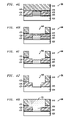
- FIGS. 1A-1E utilizes a via-level mask that is aligned and overlaid to an MTJ pillar structure.
- an MTJ pillar structure 100 is first patterned using a thin conductive hard mask 110 (e.g., TaN, TiN, or Al), as shown in FIG. 1A , and then encapsulated by an inter-layer dielectric (ILD) 120 , as shown in FIG. 1B .
- ILD inter-layer dielectric
- the second approach utilizes a tall conductive hard mask (e.g., TaN, TiN, or Al) as a vertical contact, as illustrated in FIGS. 2A-2E .
- a tall conductive hard mask e.g., TaN, TiN, or Al
- the MTJ pattern is first transferred into a thick conductive layer that is deposited on top of magnetic layers. This patterned layer is then used as a hard mask to etch the magnetic structure.
- the resultant MTJ pillar structure 200 with tall hard mask 210 is shown in FIG. 2A . It is then encapsulated with dielectric layers 220 and 230 , as shown in FIG. 2B , and planarized, as shown in FIG. 2C .
- a trench 240 in the shape of a line is etched into the dielectric layers in such a manner that the hard mask protrudes into the trench, a shown in FIG. 2D .
- the trench is filled with metal, which allows the tall hard mask to serve as a vertical contact between a conductive line 250 and the MTJ pillar structure, as shown in FIG. 2E . Because the size of the hard mask scales with the size of the MTJ pillar structure, the approach provides a path for forming vertical contacts to small MTJ structures (e.g., those below 100 mm in width or diameter).
- the planarization step usually introduces non-uniformity, which is transferred into the etch process used to form the trench for the conductive line.
- the trench may be too shallow, resulting in an open circuit, or the trench may be too deep, etching to the base of the MTJ pillar structure at position 270 and causing a short circuit, as shown in FIGS. 2D and 2E . Due to these problems, the tall hard mask approach does not provide a straight-forward path for the formation of contacts for MRAM scaling.
- Embodiments of the present invention address the above-identified need by providing methods for forming and contacting pillar structures in integrated circuits such that the pillar structures are electrically connected to overlying conductive lines by self-aligned vertical contacts.
- a pillar structure that is contacted by a vertical contact is formed in an integrated circuit.
- a hard mask is formed and utilized to pattern a least a portion of the pillar structure.
- the hard mask comprises carbon.
- the hard mask is removed.
- a conductive material is then deposited in a region previously occupied by the hard mask to form the vertical contact.
- a feature comprising diamond-like carbon (DLC) is utilized as a hard mask to anisotropically etch an MTJ pillar structure.
- Dielectric materials are then deposited on the DLC hard mask such that they surround the sidewalls and the top of the hard mask. Later, the top of the DLC hard mask is exposed in part by forming a trench in the dielectric material immediately above the hard mask.
- the trench is in the shape of a conductive line (e.g., a wordline or bitline).
- the trench for the conductive line and the region previously occupied by the hard mask are filled with a conductive material. In this way a self-aligned vertical contact is formed above the MTJ pillar structure that acts to provide a contact between the pillar structure and the overlying conductive line.
- the above-described method embodiment provides a robust and easily scalable process by which to implement various kinds of pillar structures with widths or diameters less than about 100 nm in integrated circuits.
- FIGS. 1A-1E show sectional views of a first method of contacting an MTJ pillar structure.
- FIGS. 2A-2E show sectional views of a second method of contacting an MTJ pillar structure.
- FIG. 3 shows a flow diagram of a method in accordance with an illustrative embodiment of the invention for forming an MTJ memory cell.
- FIGS. 4A-4K show sectional views of an MTJ memory cell formed using the FIG. 3 method in various stages of formation.
- FIGS. 5A-5B show sectional views of an MTJ memory cell formed using the FIG. 3 method in various stages of formation with trimming of the hard mask.
- pillar structure as used herein is intended to encompass any single or multi-component feature that protrudes above the surface of the layer on which the pillar structure is disposed and which is contacted via one of its upper surfaces. While the illustrative embodiments described herein are directed at methods of forming and contacting MTJ pillar structures for use in MRAM applications, methods in accordance with aspects of the invention may be useful with many other types of pillar structures found in integrated circuits. Such alternative pillar structures may include, but are not limited to, spin-valve structures for use in MRAMs, as well phase-change memory cells for use in phase-change memories (PCMs).
- PCMs phase-change memories
- a pillar structure When considered top down (i.e., when considered in a plane perpendicular to the sectional views shown herein), a pillar structure may be of any shape (e.g., round, elliptical, square, rectangular, hexagonal, octagonal, etc.).
- FIG. 3 shows a flow diagram of a method 300 in accordance with an illustrative embodiment of the invention for forming and contacting an MTJ pillar structure such that the MTJ pillar structure is electrically connected to an overlying conductive line by a self-aligned vertical contact.
- FIGS. 4A-4K show sectional views of an MTJ memory cell 400 formed using the FIG. 3 method in various stages of its formation.
- Step 305 in FIG. 3 comprises sequentially depositing the layers of materials that will form an MTJ pillar structure 405 L, the layer of material that will form a hard mask 410 L, and a layer of material that will form a hard mask cap 415 L onto a substrate 420 , as shown in FIG. 4A .
- an actual MTJ pillar structure will typically comprise two magnetic layers and a thin dielectric layer in between the magnetic layers that acts as a tunneling barrier.
- Each magnetic layer will comprise a number of sublayers that serve various functions such as acting as barrier layers, seed layers, antiferromagnetic layers, coupling layers, and ferromagnetic layers.
- Desikan et al. in “On-chip MRAM as a High-Bandwidth Low Latency Replacement for DRAM Physical Memories,” Tech Report TR-02-47, Department of Computer Sciences, University of Texas, September 2002, for example, describes an MTJ pillar structure with a lower magnetic layer comprising five sublayers formed of Co/Fe, Ni/Fe, Mg/Fe, Pt, and W, respectively.
- the upper magnetic layer in the same device comprises three sublayers formed of Ni/Fe, Co/Fe, and Pt, respectively.
- the dielectric barrier is Al 2 O 3 .
- the components of the MTJ pillar structure are preferably deposited by sputtering.
- the hard mask comprises carbon. While graphite, hydrocarbon polymer, and diamond hard masks would fall within the scope of the invention, a hard mask comprising DLC is preferred. Because of their attractive properties, DLC films have been technologically developed for a variety of applications and, therefore, will be familiar to one skilled in the art. Such applications include tool and die coatings, optical coatings, and protective coatings for magnetic recording media. DLC is an amorphous, in most cases, hydrogenated, metastable material. Unlike diamond and graphite, DLC films lack any long-range order and typically contain a mixture of sp 3 -, sp 2 -, and sometime sp 1 -coordinated carbon (i.e., hybridized carbon) in a disordered network.
- the ratio between the carbon atoms in the different coordinations depends on deposition conditions and, in hydrogenated DLC films, has been found to be a strong function of the hydrogen content of the films. While missing a long-range order, DLC may have a medium-range order (i.e., they may be characterized by a microcrystalline phase within an amorphous phase). The properties of DLC therefore cover a wide range of values between those of diamond, graphite, and hydrocarbon polymers. The properties of DLC may be modified by adding various additives to DLC such as nitrogen, silicon, fluorine, and metal atoms.
- DLC direct current
- rf radio frequency
- PECVD plasma-enhanced chemical vapor deposition
- sputtering ion-beam deposition
- laser ablation laser ablation
- A. Grill et al. “Diamondlike Carbon Films by RF Plasma-assisted Chemical Vapor Deposition from Acetylene,” IBM Journal of Research and Development, Volume 34, Number 6, November 1990, pp. 849-857; and A. Grill, “Plasma-deposited Diamondlike Carbon and Related Materials,” IBM Journal of Research and Development, Volume 43, Number 1/2, January/March 1999, pp. 147-161, which are both incorporated by reference herein.
- the hard mask cap preferably comprises silicon nitride (i.e., Si x N y ), but other suitable materials may also be utilized. Silicon nitride is commonly deposited in semiconductor processing by, for example, low pressure chemical vapor deposition (LPCVD) using SiCl 4 and NH 3 as reactants, or by PECVD using SiH 4 and NH 3 (or N 2 ) as reactants.
- LPCVD low pressure chemical vapor deposition
- PECVD SiH 4 and NH 3 (or N 2 ) as reactants.
- Step 310 comprises patterning the layer of hard mask cap material 415 L and the layer of hard mask material 410 L to form a hard mask cap 415 and a hard mask 410 , as shown in FIG. 4B .
- Such a step is preferably achieved by depositing a photoresist on the film stack and using conventional photolithography to define an opening in the photoresist in the location and shape of the desired MTJ pillar structure. With the developed photoresist in place, an anisotropic etch process such as reactive ion etching (RIE) is then used to pattern the hard mask cap and hard mask, after which, the photoresist is stripped.
- RIE reactive ion etching
- RIE of silicon nitride is commonly accomplished using fluorine-containing reactants such as CF 4 or SF 4 in the presence of O 2 .
- RIE of DLC is conventionally performed using a plasma containing atomic oxygen or hydrogen, which react with the DLC to produce volatile species which can be pumped out of the system.
- Step 315 comprises anisotropically etching the layers of MTJ materials 405 L using the hard mask cap 415 and hard mask 410 as masking layers during the etch.
- An MTJ pillar structure 405 is thereby formed, as shown in FIG. 4C .
- This etch is preferably by RIE or ion milling.
- Ion milling also known as ion-beam etching
- RIE reactive ion milling
- Ion milling typically is an entirely mechanical process that depends on high energy ions (e.g., ionized argon) impinging on a substrate to sputter or erode surface materials.
- Ion milling is typically a highly anisotropic process.
- Step 320 comprises depositing a liner 425 on the film stack, while step 325 comprises forming a lower dielectric 430 on the film stack.
- the resultant film stack is shown in FIG. 4D .
- the liner preferably comprises the same material as the hard mask cap 415 (e.g., silicon nitride) and may be deposited using the same methods as the hard mask cap.
- the lower dielectric preferably comprises a dielectric material different from the material forming the hard mask cap. For example, if the hard mask cap comprises silicon nitride, the lower dielectric would preferably comprise silicon oxide (SiO x ). Silicon oxide is routinely deposited on semiconductor wafers by LPCVD of Si(OC 2 H 5 ) 4 (tetraethoxysilane—TEOS).
- Step 330 comprises planarizing the lower dielectric 430 down to the liner 425 , resulting in the film stack shown in FIG. 4E .
- Such planarization may be accomplished by conventional chemical mechanical polishing (CMP).
- Step 335 comprises depositing an etch stop 435 on the planarized film stack, as shown in FIG. 4F .
- the etch stop preferably comprises the same material as the hard mask cap 415 (e.g., silicon nitride) and may be formed using similar deposition processes as those used to deposit the hard mask cap.
- Step 340 comprises depositing an upper dielectric 440 , resulting in the film stack shown in FIG. 4G .
- the upper dielectric preferably comprises the same material as the lower dielectric 430 (e.g., silicon oxide) and may be formed using similar deposition processes as those used to deposit the lower dielectric.
- Step 345 comprises anisotropically etching a trench 445 into the upper dielectric 435 .
- the trench preferably lands on the etch stop 435 , as shown in FIG. 4H .
- the trench may have the shape of a line so as to form a conductive line (e.g., wordline or bitline) for the underlying MTJ pillar structure 405 .
- the trench may be formed by conventional photolithography and RIE processes.
- the etch is preferably designed to selectively etch the upper dielectric 440 without etching, or only very slowly etching, the etch stop. In this way, the trench etch can proceed all the way to the etch stop without the possibility of progressing beyond this layer and damaging the underlying features.
- the upper dielectric comprises silicon oxide and the etch stop comprises silicon nitride
- a selective etch process can be accomplished by conventional RIE using a fluorocarbon plasma.
- U.S. Pat. No. 5,268,344 entitled “Process for Selectively Etching a Layer of Silicon Dioxide on an Underlying Stop Layer of Silicon Nitride” (incorporated by reference herein), for example, describes the use a combination of CHF 3 , CF 4 , CH 2 F 2 , and Ar to selectively etch silicon oxide with a selectivity of oxide-to-nitride of about 30:1.
- Step 350 comprises anisotropically etching the exposed etch stop 435 , liner 425 , and hard mask cap 415 selectively to the exposed surfaces of the lower dielectric 430 , the upper dielectric 440 , and the hard mask 410 .
- the upper surface of the hard mask is exposed, as shown in FIG. 4 I.
- the etch stop, liner, and hard mask cap comprise silicon nitride
- the hard mask comprises DLC
- the upper dielectric and lower dielectric comprise silicon oxide
- 4,717,447 entitled “Method of Manufacturing a Semiconductor Device by Means of Plasma Etching” (incorporated by reference herein) describes the use of a combination of CF 3 Br, F, and He to achieve a nitride-to-oxide selectivity of about 19:1.
- U.S. Pat. No. 4,568,410 entitled “Selective Plasma Etching of Silicon Nitride in the Presence of Silicon Dioxide” (incorporated by reference herein), describes the use of a mixture of NF 3 and O 2 to achieve nitride-to-oxide selectivities in excess of about 8:1.
- Step 355 comprises anisotropically etching the exposed hard mask 410 so that it is entirely removed from the film stack and the MTJ pillar structure 405 is exposed, as shown in FIG. 4J .
- This etch can again be performed by RIE using a plasma including atomic oxygen or hydrogen.
- Step 360 comprises simultaneously depositing a conformal conductive material into the region previously occupied by the hard mask 410 , the hard mask cap 415 , and some of the liner 425 , as well as into the trench 445 .
- the conductive material may comprise metallic materials such as, but not limited to, Al, Cu, W, Ti, Ta, or alloys thereof, and may be deposited by conventional chemical vapor deposition, sputtering, or plating techniques.
- a thin metallic liner e.g., Ti and/or TiN
- any excess conductive material is planarized by, for example, CMP such that any excess material is removed from the top of the upper dielectric 440 , as shown in FIG. 4K .
- care is preferably taken to avoid any residual conductive material on the upper dielectric that may cause shorting.
- a vertical contact 450 that is self-aligned to the MTJ pillar structure 405 is formed. The vertical contact electrically connects the MTJ pillar structure to an overlying conductive line 455 .
- DLC for the hard mask 410 provides several advantages over the use of other types of materials such as metallic materials. If the MTJ pillar structure 405 is formed by ion milling in step 315 , for example, the possibility of sidewall redeposition during the milling is reduced because DLC has a very low sputter yield due to its relative hardness. DLC is also resistant to most wet chemical etches which may be required to clean the sidewalls of the MTJ pillar structure after it is etched or ion milled. Moreover, DLC can be easily removed from the top of MTJ pillar structure in step 355 by using a plasma of atomic oxygen or hydrogen.
- Such an etch process is relatively mild and benign when compared to, for example, the halogen-based etch chemistries required to etch alternative hard mask materials (e.g., TaN, TiN, or Al). Such a mild etch process is less likely to negatively impact (e.g., poison) those materials constituting the MTJ pillar structure.
- alternative hard mask materials e.g., TaN, TiN, or Al.
- DLC also has the advantage of being a very effective polish stop material, again, because of its relative hardness.
- this property allows the option of planarizing the lower dielectric 430 to the hard mask 410 in step 330 instead of planarizing it to the liner 425 .
- Such an option may be advantageous if difficulty is encountered when trying to stop a planarization process on the relatively thin liner. Planarizing to the hard mask in this manner does not substantially alter the remainder of the steps in the illustrative method.
- DLC further has the advantage of being easily trimmed, that is, having its width or diameter reduced while its height is left unchanged.
- An optional trimming step 318 is shown in FIG. 3 and is preferably performed between steps 315 and 320 . It may be accomplished by using an etch process that etches the hard mask 410 without substantially etching the hard mask cap 415 or MTJ pillar structure 405 . For DLC, such an etch process may be accomplished by exposing the DLC to a plasma comprising atomic oxygen or hydrogen without placing a substantial bias on the substrate being etched. Operating without a substantial bias allows the etch to be considerably isotropic.
- FIG. 5A shows the film stack after the optional trimming step 318 .
- FIG. 5B shows the film stack after step 365 is completed.
- the optional trimming step has the effect of narrowing the resultant vertical contact 450 . Narrowing the vertical contact may be beneficial in some applications to avoid the possibility of the vertical contact shorting to other nearby active features.
- DLC also provides advantages with respect to device characterization.
- conventional MTJ memory cell formation techniques typically use a metallic hard mask feature.
- This metallic feature may interfere with Kerr magnetometry measurements, a very useful method for studying magnetic anisotropy in ferromagnetic films in MRAM devices.
- Kerr magnetometry measures the rotation of the polarization of light reflected from the surface of a magnetic material under study as a function of applied magnetic field. The Kerr signal is proportional to the magnetic moment of the sample under test.
- a hard mask comprising DLC will not interfere with these optical measurements because DLC is transparent to the light used in Kerr analysis, thereby allowing Kerr measurements to be obtained with the DLC hard mask in place.
- Kerr measurements may be accomplished after hard mask is removed and before the film stack is filled with conductive material.
- the chip design is created in a graphical computer programming language, and is stored in a computer storage medium (such as a disk, tape, physical hard drive, or virtual hard drive such as in a storage access network). If the designer does not fabricate chips or photolithographic masks used to fabricate chips, the designer transmits the resulting design by physical means (e.g., by providing a copy of the storage medium storing the design) or electronically (e.g., through the Internet) to such entities, directly or indirectly.
- the stored design is then converted into the appropriate format (e.g., GDSII) for the fabrication of photolithographic masks, which typically include multiple copies of the chip design in question that are formed on a wafer.
- the photolithographic masks are utilized to define areas of the wafer (and/or the layers thereon) to be etched or otherwise processed.
- the resulting integrated circuit chips may be distributed by the fabricator in raw wafer form (i.e., as a single wafer that has multiple unpackaged chips), as a bare die, or in packaged form.
- the chip is mounted in a single chip package (e.g., plastic carrier with leads that are affixed to a motherboard or other higher level carrier) or in a multichip package (e.g., ceramic carrier that has either or both surface interconnections or buried interconnections).
- the chip is then integrated with other chips, discrete circuit elements, and/or other signal processing devices as part of either an intermediate product (e.g., motherboard) or an end product.
- the end product may be any product that includes integrated circuit chips, ranging from toys and other low-end applications to advanced computer products having a display, a keyboard or other input device, and a central processor.
Abstract
Description
Claims (16)
Priority Applications (1)
| Application Number | Priority Date | Filing Date | Title |
|---|---|---|---|
| US11/866,455 US8008095B2 (en) | 2007-10-03 | 2007-10-03 | Methods for fabricating contacts to pillar structures in integrated circuits |
Applications Claiming Priority (1)
| Application Number | Priority Date | Filing Date | Title |
|---|---|---|---|
| US11/866,455 US8008095B2 (en) | 2007-10-03 | 2007-10-03 | Methods for fabricating contacts to pillar structures in integrated circuits |
Publications (2)
| Publication Number | Publication Date |
|---|---|
| US20090091037A1 US20090091037A1 (en) | 2009-04-09 |
| US8008095B2 true US8008095B2 (en) | 2011-08-30 |
Family
ID=40522573
Family Applications (1)
| Application Number | Title | Priority Date | Filing Date |
|---|---|---|---|
| US11/866,455 Expired - Fee Related US8008095B2 (en) | 2007-10-03 | 2007-10-03 | Methods for fabricating contacts to pillar structures in integrated circuits |
Country Status (1)
| Country | Link |
|---|---|
| US (1) | US8008095B2 (en) |
Cited By (44)
| Publication number | Priority date | Publication date | Assignee | Title |
|---|---|---|---|---|
| US9583358B2 (en) | 2014-05-30 | 2017-02-28 | Samsung Electronics Co., Ltd. | Hardmask composition and method of forming pattern by using the hardmask composition |
| US9721794B2 (en) | 2014-07-25 | 2017-08-01 | Samsung Electronics Co., Ltd. | Hardmask composition and method of forming patterning by using the hardmask composition |
| US9728717B2 (en) | 2015-03-03 | 2017-08-08 | International Business Machines Corporation | Magnetic tunnel junction patterning using low atomic weight ion sputtering |
| US20170256708A1 (en) * | 2016-03-07 | 2017-09-07 | Samsung Electronics Co., Ltd. | Method and system for providing a magnetic junction usable in spin transfer torque applications using multiple stack depositions |
| US10109675B2 (en) | 2017-03-08 | 2018-10-23 | International Business Machines Corporation | Forming self-aligned contacts on pillar structures |
| US10133176B2 (en) | 2015-03-24 | 2018-11-20 | Samsung Electronics Co., Ltd. | Hardmask composition and method of forming pattern using the same |
| US10331033B2 (en) | 2014-07-04 | 2019-06-25 | Samsung Electronics Co., Ltd. | Hardmask composition and method of forming pattern using the hardmask composition |
| US10360962B1 (en) | 2017-12-28 | 2019-07-23 | Spin Memory, Inc. | Memory array with individually trimmable sense amplifiers |
| US10360964B2 (en) | 2016-09-27 | 2019-07-23 | Spin Memory, Inc. | Method of writing contents in memory during a power up sequence using a dynamic redundancy register in a memory device |
| US10366774B2 (en) | 2016-09-27 | 2019-07-30 | Spin Memory, Inc. | Device with dynamic redundancy registers |
| US10388862B1 (en) | 2018-04-12 | 2019-08-20 | Taiwan Semiconductor Manufacturing Company, Ltd. | Highly selective ion beam etch hard mask for sub 60nm MRAM devices |
| US10395712B2 (en) | 2017-12-28 | 2019-08-27 | Spin Memory, Inc. | Memory array with horizontal source line and sacrificial bitline per virtual source |
| US10395711B2 (en) | 2017-12-28 | 2019-08-27 | Spin Memory, Inc. | Perpendicular source and bit lines for an MRAM array |
| US10411185B1 (en) | 2018-05-30 | 2019-09-10 | Spin Memory, Inc. | Process for creating a high density magnetic tunnel junction array test platform |
| US10437723B2 (en) | 2016-09-27 | 2019-10-08 | Spin Memory, Inc. | Method of flushing the contents of a dynamic redundancy register to a secure storage area during a power down in a memory device |
| US10437491B2 (en) | 2016-09-27 | 2019-10-08 | Spin Memory, Inc. | Method of processing incomplete memory operations in a memory device during a power up sequence and a power down sequence using a dynamic redundancy register |
| US10446744B2 (en) | 2018-03-08 | 2019-10-15 | Spin Memory, Inc. | Magnetic tunnel junction wafer adaptor used in magnetic annealing furnace and method of using the same |
| US10481976B2 (en) | 2017-10-24 | 2019-11-19 | Spin Memory, Inc. | Forcing bits as bad to widen the window between the distributions of acceptable high and low resistive bits thereby lowering the margin and increasing the speed of the sense amplifiers |
| US10489245B2 (en) | 2017-10-24 | 2019-11-26 | Spin Memory, Inc. | Forcing stuck bits, waterfall bits, shunt bits and low TMR bits to short during testing and using on-the-fly bit failure detection and bit redundancy remapping techniques to correct them |
| US10495972B2 (en) | 2015-04-03 | 2019-12-03 | Samsung Electronics Co., Ltd. | Hardmask composition and method of forming pattern using the hardmask composition |
| US10529915B2 (en) | 2018-03-23 | 2020-01-07 | Spin Memory, Inc. | Bit line structures for three-dimensional arrays with magnetic tunnel junction devices including an annular free magnetic layer and a planar reference magnetic layer |
| US10529439B2 (en) | 2017-10-24 | 2020-01-07 | Spin Memory, Inc. | On-the-fly bit failure detection and bit redundancy remapping techniques to correct for fixed bit defects |
| US10546624B2 (en) | 2017-12-29 | 2020-01-28 | Spin Memory, Inc. | Multi-port random access memory |
| US10546625B2 (en) | 2016-09-27 | 2020-01-28 | Spin Memory, Inc. | Method of optimizing write voltage based on error buffer occupancy |
| US10593396B2 (en) | 2018-07-06 | 2020-03-17 | Spin Memory, Inc. | Multi-bit cell read-out techniques for MRAM cells with mixed pinned magnetization orientations |
| US10600478B2 (en) | 2018-07-06 | 2020-03-24 | Spin Memory, Inc. | Multi-bit cell read-out techniques for MRAM cells with mixed pinned magnetization orientations |
| US10650875B2 (en) | 2018-08-21 | 2020-05-12 | Spin Memory, Inc. | System for a wide temperature range nonvolatile memory |
| US10656994B2 (en) | 2017-10-24 | 2020-05-19 | Spin Memory, Inc. | Over-voltage write operation of tunnel magnet-resistance (“TMR”) memory device and correcting failure bits therefrom by using on-the-fly bit failure detection and bit redundancy remapping techniques |
| US10685844B2 (en) | 2017-07-27 | 2020-06-16 | Samsung Electronics Co., Ltd. | Hardmask composition, method of forming pattern by using the hardmask composition, and hardmask formed using the hardmask composition |
| US10741753B2 (en) | 2016-03-11 | 2020-08-11 | Micron Technology, Inc. | Conductive hard mask for memory device formation |
| US10784437B2 (en) | 2018-03-23 | 2020-09-22 | Spin Memory, Inc. | Three-dimensional arrays with MTJ devices including a free magnetic trench layer and a planar reference magnetic layer |
| US10811594B2 (en) | 2017-12-28 | 2020-10-20 | Spin Memory, Inc. | Process for hard mask development for MRAM pillar formation using photolithography |
| US10808142B2 (en) | 2017-07-28 | 2020-10-20 | Samsung Electronics Co., Ltd. | Method of preparing graphene quantum dot, hardmask composition including the graphene quantum dot obtained by the method, method of forming patterns using the hardmask composition, and hardmask formed from the hardmask composition |
| US10818331B2 (en) | 2016-09-27 | 2020-10-27 | Spin Memory, Inc. | Multi-chip module for MRAM devices with levels of dynamic redundancy registers |
| US10840439B2 (en) | 2017-12-29 | 2020-11-17 | Spin Memory, Inc. | Magnetic tunnel junction (MTJ) fabrication methods and systems |
| US10840441B2 (en) | 2018-09-14 | 2020-11-17 | International Business Machines Corporation | Diamond-like carbon hardmask for MRAM |
| US10886330B2 (en) | 2017-12-29 | 2021-01-05 | Spin Memory, Inc. | Memory device having overlapping magnetic tunnel junctions in compliance with a reference pitch |
| US10891997B2 (en) | 2017-12-28 | 2021-01-12 | Spin Memory, Inc. | Memory array with horizontal source line and a virtual source line |
| US10971680B2 (en) | 2018-10-01 | 2021-04-06 | Spin Memory, Inc. | Multi terminal device stack formation methods |
| US11034847B2 (en) | 2017-07-14 | 2021-06-15 | Samsung Electronics Co., Ltd. | Hardmask composition, method of forming pattern using hardmask composition, and hardmask formed from hardmask composition |
| US11107979B2 (en) | 2018-12-28 | 2021-08-31 | Spin Memory, Inc. | Patterned silicide structures and methods of manufacture |
| US11107978B2 (en) | 2018-03-23 | 2021-08-31 | Spin Memory, Inc. | Methods of manufacturing three-dimensional arrays with MTJ devices including a free magnetic trench layer and a planar reference magnetic layer |
| US11107974B2 (en) | 2018-03-23 | 2021-08-31 | Spin Memory, Inc. | Magnetic tunnel junction devices including a free magnetic trench layer and a planar reference magnetic layer |
| US11621293B2 (en) | 2018-10-01 | 2023-04-04 | Integrated Silicon Solution, (Cayman) Inc. | Multi terminal device stack systems and methods |
Families Citing this family (61)
| Publication number | Priority date | Publication date | Assignee | Title |
|---|---|---|---|---|
| KR101435001B1 (en) * | 2007-12-20 | 2014-08-29 | 삼성전자주식회사 | Phase Changeable Memory And Method Of Fabricating The Same |
| US7883946B1 (en) | 2008-05-08 | 2011-02-08 | Altera Corporation | Angled implantation for deep submicron device optimization |
| US8962493B2 (en) | 2010-12-13 | 2015-02-24 | Crocus Technology Inc. | Magnetic random access memory cells having improved size and shape characteristics |
| US20130075840A1 (en) * | 2011-02-09 | 2013-03-28 | Avalanche Technology, Inc. | Method for fabrication of a magnetic random access memory (mram) using a high selectivity hard mask |
| KR20130016827A (en) * | 2011-08-09 | 2013-02-19 | 에스케이하이닉스 주식회사 | Semiconductor device and method for fabricating the same |
| US8835898B2 (en) | 2012-04-20 | 2014-09-16 | International Business Machines Corporation | Self-aligned process to fabricate a memory cell array with a surrounding-gate access transistor |
| JP2014106996A (en) * | 2012-11-29 | 2014-06-09 | Toshiba Corp | Perpendicular magnetic recording medium, and manufacturing method of the same |
| US9263667B1 (en) * | 2014-07-25 | 2016-02-16 | Spin Transfer Technologies, Inc. | Method for manufacturing MTJ memory device |
| TWI670831B (en) | 2014-09-03 | 2019-09-01 | 美商應用材料股份有限公司 | Nanocrystalline diamond carbon film for 3d nand hardmask application |
| US9337412B2 (en) | 2014-09-22 | 2016-05-10 | Spin Transfer Technologies, Inc. | Magnetic tunnel junction structure for MRAM device |
| US10468590B2 (en) | 2015-04-21 | 2019-11-05 | Spin Memory, Inc. | High annealing temperature perpendicular magnetic anisotropy structure for magnetic random access memory |
| US9728712B2 (en) | 2015-04-21 | 2017-08-08 | Spin Transfer Technologies, Inc. | Spin transfer torque structure for MRAM devices having a spin current injection capping layer |
| US9853206B2 (en) | 2015-06-16 | 2017-12-26 | Spin Transfer Technologies, Inc. | Precessional spin current structure for MRAM |
| US9773974B2 (en) | 2015-07-30 | 2017-09-26 | Spin Transfer Technologies, Inc. | Polishing stop layer(s) for processing arrays of semiconductor elements |
| US10163479B2 (en) | 2015-08-14 | 2018-12-25 | Spin Transfer Technologies, Inc. | Method and apparatus for bipolar memory write-verify |
| US9484373B1 (en) | 2015-11-18 | 2016-11-01 | Omnivision Technologies, Inc. | Hard mask as contact etch stop layer in image sensors |
| US9647200B1 (en) | 2015-12-07 | 2017-05-09 | International Business Machines Corporation | Encapsulation of magnetic tunnel junction structures in organic photopatternable dielectric material |
| US9741926B1 (en) | 2016-01-28 | 2017-08-22 | Spin Transfer Technologies, Inc. | Memory cell having magnetic tunnel junction and thermal stability enhancement layer |
| KR20190038945A (en) * | 2016-08-29 | 2019-04-09 | 도쿄엘렉트론가부시키가이샤 | Semi-atomic layer etching method of silicon nitride |
| US10217670B2 (en) * | 2016-09-07 | 2019-02-26 | Tokyo Electron Limited | Wrap-around contact integration scheme |
| US11151042B2 (en) | 2016-09-27 | 2021-10-19 | Integrated Silicon Solution, (Cayman) Inc. | Error cache segmentation for power reduction |
| US10446210B2 (en) | 2016-09-27 | 2019-10-15 | Spin Memory, Inc. | Memory instruction pipeline with a pre-read stage for a write operation for reducing power consumption in a memory device that uses dynamic redundancy registers |
| US10628316B2 (en) | 2016-09-27 | 2020-04-21 | Spin Memory, Inc. | Memory device with a plurality of memory banks where each memory bank is associated with a corresponding memory instruction pipeline and a dynamic redundancy register |
| US10991410B2 (en) | 2016-09-27 | 2021-04-27 | Spin Memory, Inc. | Bi-polar write scheme |
| US11119910B2 (en) | 2016-09-27 | 2021-09-14 | Spin Memory, Inc. | Heuristics for selecting subsegments for entry in and entry out operations in an error cache system with coarse and fine grain segments |
| US10460781B2 (en) | 2016-09-27 | 2019-10-29 | Spin Memory, Inc. | Memory device with a dual Y-multiplexer structure for performing two simultaneous operations on the same row of a memory bank |
| US11119936B2 (en) | 2016-09-27 | 2021-09-14 | Spin Memory, Inc. | Error cache system with coarse and fine segments for power optimization |
| US10446405B2 (en) | 2017-02-23 | 2019-10-15 | Tokyo Electron Limited | Method of anisotropic extraction of silicon nitride mandrel for fabrication of self-aligned block structures |
| TWI756367B (en) | 2017-02-23 | 2022-03-01 | 日商東京威力科創股份有限公司 | Method of quasi-atomic layer etching of silicon nitride |
| US10665777B2 (en) | 2017-02-28 | 2020-05-26 | Spin Memory, Inc. | Precessional spin current structure with non-magnetic insertion layer for MRAM |
| US10672976B2 (en) | 2017-02-28 | 2020-06-02 | Spin Memory, Inc. | Precessional spin current structure with high in-plane magnetization for MRAM |
| US10032978B1 (en) | 2017-06-27 | 2018-07-24 | Spin Transfer Technologies, Inc. | MRAM with reduced stray magnetic fields |
| US10679685B2 (en) | 2017-12-27 | 2020-06-09 | Spin Memory, Inc. | Shared bit line array architecture for magnetoresistive memory |
| US10424726B2 (en) | 2017-12-28 | 2019-09-24 | Spin Memory, Inc. | Process for improving photoresist pillar adhesion during MRAM fabrication |
| US10516094B2 (en) | 2017-12-28 | 2019-12-24 | Spin Memory, Inc. | Process for creating dense pillars using multiple exposures for MRAM fabrication |
| US10840436B2 (en) | 2017-12-29 | 2020-11-17 | Spin Memory, Inc. | Perpendicular magnetic anisotropy interface tunnel junction devices and methods of manufacture |
| US10360961B1 (en) | 2017-12-29 | 2019-07-23 | Spin Memory, Inc. | AC current pre-charge write-assist in orthogonal STT-MRAM |
| US10270027B1 (en) | 2017-12-29 | 2019-04-23 | Spin Memory, Inc. | Self-generating AC current assist in orthogonal STT-MRAM |
| US10199083B1 (en) | 2017-12-29 | 2019-02-05 | Spin Transfer Technologies, Inc. | Three-terminal MRAM with ac write-assist for low read disturb |
| US10784439B2 (en) | 2017-12-29 | 2020-09-22 | Spin Memory, Inc. | Precessional spin current magnetic tunnel junction devices and methods of manufacture |
| US10236048B1 (en) | 2017-12-29 | 2019-03-19 | Spin Memory, Inc. | AC current write-assist in orthogonal STT-MRAM |
| US10367139B2 (en) | 2017-12-29 | 2019-07-30 | Spin Memory, Inc. | Methods of manufacturing magnetic tunnel junction devices |
| US10236047B1 (en) | 2017-12-29 | 2019-03-19 | Spin Memory, Inc. | Shared oscillator (STNO) for MRAM array write-assist in orthogonal STT-MRAM |
| US10424723B2 (en) | 2017-12-29 | 2019-09-24 | Spin Memory, Inc. | Magnetic tunnel junction devices including an optimization layer |
| US10229724B1 (en) | 2017-12-30 | 2019-03-12 | Spin Memory, Inc. | Microwave write-assist in series-interconnected orthogonal STT-MRAM devices |
| US10141499B1 (en) | 2017-12-30 | 2018-11-27 | Spin Transfer Technologies, Inc. | Perpendicular magnetic tunnel junction device with offset precessional spin current layer |
| US10255962B1 (en) | 2017-12-30 | 2019-04-09 | Spin Memory, Inc. | Microwave write-assist in orthogonal STT-MRAM |
| US10319900B1 (en) | 2017-12-30 | 2019-06-11 | Spin Memory, Inc. | Perpendicular magnetic tunnel junction device with precessional spin current layer having a modulated moment density |
| US10339993B1 (en) | 2017-12-30 | 2019-07-02 | Spin Memory, Inc. | Perpendicular magnetic tunnel junction device with skyrmionic assist layers for free layer switching |
| US10236439B1 (en) | 2017-12-30 | 2019-03-19 | Spin Memory, Inc. | Switching and stability control for perpendicular magnetic tunnel junction device |
| US10468588B2 (en) | 2018-01-05 | 2019-11-05 | Spin Memory, Inc. | Perpendicular magnetic tunnel junction device with skyrmionic enhancement layers for the precessional spin current magnetic layer |
| US10438996B2 (en) | 2018-01-08 | 2019-10-08 | Spin Memory, Inc. | Methods of fabricating magnetic tunnel junctions integrated with selectors |
| US10438995B2 (en) | 2018-01-08 | 2019-10-08 | Spin Memory, Inc. | Devices including magnetic tunnel junctions integrated with selectors |
| US10388861B1 (en) | 2018-03-08 | 2019-08-20 | Spin Memory, Inc. | Magnetic tunnel junction wafer adaptor used in magnetic annealing furnace and method of using the same |
| US10559338B2 (en) | 2018-07-06 | 2020-02-11 | Spin Memory, Inc. | Multi-bit cell read-out techniques |
| US10692569B2 (en) | 2018-07-06 | 2020-06-23 | Spin Memory, Inc. | Read-out techniques for multi-bit cells |
| US10699761B2 (en) | 2018-09-18 | 2020-06-30 | Spin Memory, Inc. | Word line decoder memory architecture |
| US10580827B1 (en) | 2018-11-16 | 2020-03-03 | Spin Memory, Inc. | Adjustable stabilizer/polarizer method for MRAM with enhanced stability and efficient switching |
| US11315870B2 (en) * | 2018-11-21 | 2022-04-26 | Globalfoundries U.S. Inc. | Top electrode interconnect structures |
| US10727398B1 (en) * | 2019-01-30 | 2020-07-28 | International Business Machines Corporation | MTJ containing device containing a bottom electrode embedded in diamond-like carbon |
| EP4002437B1 (en) * | 2020-09-22 | 2023-08-02 | Changxin Memory Technologies, Inc. | Method of forming a contact window structure |
Citations (11)
| Publication number | Priority date | Publication date | Assignee | Title |
|---|---|---|---|---|
| US4568410A (en) | 1984-12-20 | 1986-02-04 | Motorola, Inc. | Selective plasma etching of silicon nitride in the presence of silicon oxide |
| US4717447A (en) | 1982-11-16 | 1988-01-05 | U.S. Philips Corporation | Method of manufacturing a semiconductor device by means of plasma etching |
| US5286344A (en) | 1992-06-15 | 1994-02-15 | Micron Technology, Inc. | Process for selectively etching a layer of silicon dioxide on an underlying stop layer of silicon nitride |
| US5559367A (en) | 1994-07-12 | 1996-09-24 | International Business Machines Corporation | Diamond-like carbon for use in VLSI and ULSI interconnect systems |
| US5928967A (en) | 1996-06-10 | 1999-07-27 | International Business Machines Corporation | Selective oxide-to-nitride etch process using C4 F8 /CO/Ar |
| US20040100855A1 (en) * | 2002-11-22 | 2004-05-27 | Kabushiki Kaisha Toshiba | Magneto-resistance effect element, magnetic memory and magnetic head |
| US6767837B2 (en) * | 2002-10-01 | 2004-07-27 | Nanya Technology Corporation | Etch-back method for dielectric layer |
| US6784091B1 (en) * | 2003-06-05 | 2004-08-31 | International Business Machines Corporation | Maskless array protection process flow for forming interconnect vias in magnetic random access memory devices |
| US6933155B2 (en) * | 2003-05-21 | 2005-08-23 | Grandis, Inc. | Methods for providing a sub .15 micron magnetic memory structure |
| US20050287738A1 (en) * | 2004-06-24 | 2005-12-29 | Cho Sung-Il | Method of manufacturing a semiconductor memory device |
| US7205164B1 (en) * | 2005-01-19 | 2007-04-17 | Silicon Magnetic Systems | Methods for fabricating magnetic cell junctions and a structure resulting and/or used for such methods |
-
2007
- 2007-10-03 US US11/866,455 patent/US8008095B2/en not_active Expired - Fee Related
Patent Citations (11)
| Publication number | Priority date | Publication date | Assignee | Title |
|---|---|---|---|---|
| US4717447A (en) | 1982-11-16 | 1988-01-05 | U.S. Philips Corporation | Method of manufacturing a semiconductor device by means of plasma etching |
| US4568410A (en) | 1984-12-20 | 1986-02-04 | Motorola, Inc. | Selective plasma etching of silicon nitride in the presence of silicon oxide |
| US5286344A (en) | 1992-06-15 | 1994-02-15 | Micron Technology, Inc. | Process for selectively etching a layer of silicon dioxide on an underlying stop layer of silicon nitride |
| US5559367A (en) | 1994-07-12 | 1996-09-24 | International Business Machines Corporation | Diamond-like carbon for use in VLSI and ULSI interconnect systems |
| US5928967A (en) | 1996-06-10 | 1999-07-27 | International Business Machines Corporation | Selective oxide-to-nitride etch process using C4 F8 /CO/Ar |
| US6767837B2 (en) * | 2002-10-01 | 2004-07-27 | Nanya Technology Corporation | Etch-back method for dielectric layer |
| US20040100855A1 (en) * | 2002-11-22 | 2004-05-27 | Kabushiki Kaisha Toshiba | Magneto-resistance effect element, magnetic memory and magnetic head |
| US6933155B2 (en) * | 2003-05-21 | 2005-08-23 | Grandis, Inc. | Methods for providing a sub .15 micron magnetic memory structure |
| US6784091B1 (en) * | 2003-06-05 | 2004-08-31 | International Business Machines Corporation | Maskless array protection process flow for forming interconnect vias in magnetic random access memory devices |
| US20050287738A1 (en) * | 2004-06-24 | 2005-12-29 | Cho Sung-Il | Method of manufacturing a semiconductor memory device |
| US7205164B1 (en) * | 2005-01-19 | 2007-04-17 | Silicon Magnetic Systems | Methods for fabricating magnetic cell junctions and a structure resulting and/or used for such methods |
Non-Patent Citations (3)
| Title |
|---|
| A. Grill et al, "Diamondlike carbon films by rf plasma-assisted chemical vapor deposition from acetylene," IBM J. Res. Develop., Nov. 1990, pp. 849-857, vol. 34, No. 6, IBM. |
| A. Grill, "Plasma-deposited diamondlike carbon and related materials," IBM J. Res. Develop., Jan./Mar. 1999, pp. 147-161, vol. 43, No. 1/2, IBM. |
| R. Desikan et al., "On-chip MRAM as a High-Bandwidth Low-Latency Replacement for DRAM Physical Memories," Tech Report TR-O2-47, Sep. 2002, Dept. of Computer Sciences, University of Texas. |
Cited By (56)
| Publication number | Priority date | Publication date | Assignee | Title |
|---|---|---|---|---|
| US9583358B2 (en) | 2014-05-30 | 2017-02-28 | Samsung Electronics Co., Ltd. | Hardmask composition and method of forming pattern by using the hardmask composition |
| US10170325B2 (en) | 2014-05-30 | 2019-01-01 | Samsung Electronics Co., Ltd. | Hardmask composition and method of forming pattern by using the hardmask composition |
| US10331033B2 (en) | 2014-07-04 | 2019-06-25 | Samsung Electronics Co., Ltd. | Hardmask composition and method of forming pattern using the hardmask composition |
| US9721794B2 (en) | 2014-07-25 | 2017-08-01 | Samsung Electronics Co., Ltd. | Hardmask composition and method of forming patterning by using the hardmask composition |
| US10153163B2 (en) | 2014-07-25 | 2018-12-11 | Samsung Electronics Co., Ltd. | Hardmask composition and method of forming patterning by using the hardmask composition |
| US9728717B2 (en) | 2015-03-03 | 2017-08-08 | International Business Machines Corporation | Magnetic tunnel junction patterning using low atomic weight ion sputtering |
| US10133176B2 (en) | 2015-03-24 | 2018-11-20 | Samsung Electronics Co., Ltd. | Hardmask composition and method of forming pattern using the same |
| US10495972B2 (en) | 2015-04-03 | 2019-12-03 | Samsung Electronics Co., Ltd. | Hardmask composition and method of forming pattern using the hardmask composition |
| US11086223B2 (en) | 2015-04-03 | 2021-08-10 | Samsung Electronics Co., Ltd. | Hardmask composition and method of forming pattern using the hardmask composition |
| US20170256708A1 (en) * | 2016-03-07 | 2017-09-07 | Samsung Electronics Co., Ltd. | Method and system for providing a magnetic junction usable in spin transfer torque applications using multiple stack depositions |
| US10164175B2 (en) * | 2016-03-07 | 2018-12-25 | Samsung Electronics Co., Ltd. | Method and system for providing a magnetic junction usable in spin transfer torque applications using multiple stack depositions |
| US10741753B2 (en) | 2016-03-11 | 2020-08-11 | Micron Technology, Inc. | Conductive hard mask for memory device formation |
| US10366774B2 (en) | 2016-09-27 | 2019-07-30 | Spin Memory, Inc. | Device with dynamic redundancy registers |
| US10437491B2 (en) | 2016-09-27 | 2019-10-08 | Spin Memory, Inc. | Method of processing incomplete memory operations in a memory device during a power up sequence and a power down sequence using a dynamic redundancy register |
| US10546625B2 (en) | 2016-09-27 | 2020-01-28 | Spin Memory, Inc. | Method of optimizing write voltage based on error buffer occupancy |
| US10818331B2 (en) | 2016-09-27 | 2020-10-27 | Spin Memory, Inc. | Multi-chip module for MRAM devices with levels of dynamic redundancy registers |
| US10366775B2 (en) | 2016-09-27 | 2019-07-30 | Spin Memory, Inc. | Memory device using levels of dynamic redundancy registers for writing a data word that failed a write operation |
| US10360964B2 (en) | 2016-09-27 | 2019-07-23 | Spin Memory, Inc. | Method of writing contents in memory during a power up sequence using a dynamic redundancy register in a memory device |
| US10424393B2 (en) | 2016-09-27 | 2019-09-24 | Spin Memory, Inc. | Method of reading data from a memory device using multiple levels of dynamic redundancy registers |
| US10437723B2 (en) | 2016-09-27 | 2019-10-08 | Spin Memory, Inc. | Method of flushing the contents of a dynamic redundancy register to a secure storage area during a power down in a memory device |
| US10586921B2 (en) | 2017-03-08 | 2020-03-10 | International Business Machines Corporation | Forming self-aligned contacts on pillar structures |
| US10586920B2 (en) | 2017-03-08 | 2020-03-10 | International Business Machines Corporation | Forming self-aligned contacts on pillar structures |
| US10109675B2 (en) | 2017-03-08 | 2018-10-23 | International Business Machines Corporation | Forming self-aligned contacts on pillar structures |
| US11034847B2 (en) | 2017-07-14 | 2021-06-15 | Samsung Electronics Co., Ltd. | Hardmask composition, method of forming pattern using hardmask composition, and hardmask formed from hardmask composition |
| US10685844B2 (en) | 2017-07-27 | 2020-06-16 | Samsung Electronics Co., Ltd. | Hardmask composition, method of forming pattern by using the hardmask composition, and hardmask formed using the hardmask composition |
| US10808142B2 (en) | 2017-07-28 | 2020-10-20 | Samsung Electronics Co., Ltd. | Method of preparing graphene quantum dot, hardmask composition including the graphene quantum dot obtained by the method, method of forming patterns using the hardmask composition, and hardmask formed from the hardmask composition |
| US10529439B2 (en) | 2017-10-24 | 2020-01-07 | Spin Memory, Inc. | On-the-fly bit failure detection and bit redundancy remapping techniques to correct for fixed bit defects |
| US10489245B2 (en) | 2017-10-24 | 2019-11-26 | Spin Memory, Inc. | Forcing stuck bits, waterfall bits, shunt bits and low TMR bits to short during testing and using on-the-fly bit failure detection and bit redundancy remapping techniques to correct them |
| US10481976B2 (en) | 2017-10-24 | 2019-11-19 | Spin Memory, Inc. | Forcing bits as bad to widen the window between the distributions of acceptable high and low resistive bits thereby lowering the margin and increasing the speed of the sense amplifiers |
| US10656994B2 (en) | 2017-10-24 | 2020-05-19 | Spin Memory, Inc. | Over-voltage write operation of tunnel magnet-resistance (“TMR”) memory device and correcting failure bits therefrom by using on-the-fly bit failure detection and bit redundancy remapping techniques |
| US10811594B2 (en) | 2017-12-28 | 2020-10-20 | Spin Memory, Inc. | Process for hard mask development for MRAM pillar formation using photolithography |
| US10891997B2 (en) | 2017-12-28 | 2021-01-12 | Spin Memory, Inc. | Memory array with horizontal source line and a virtual source line |
| US10395712B2 (en) | 2017-12-28 | 2019-08-27 | Spin Memory, Inc. | Memory array with horizontal source line and sacrificial bitline per virtual source |
| US10360962B1 (en) | 2017-12-28 | 2019-07-23 | Spin Memory, Inc. | Memory array with individually trimmable sense amplifiers |
| US10930332B2 (en) | 2017-12-28 | 2021-02-23 | Spin Memory, Inc. | Memory array with individually trimmable sense amplifiers |
| US10395711B2 (en) | 2017-12-28 | 2019-08-27 | Spin Memory, Inc. | Perpendicular source and bit lines for an MRAM array |
| US10546624B2 (en) | 2017-12-29 | 2020-01-28 | Spin Memory, Inc. | Multi-port random access memory |
| US10886330B2 (en) | 2017-12-29 | 2021-01-05 | Spin Memory, Inc. | Memory device having overlapping magnetic tunnel junctions in compliance with a reference pitch |
| US10840439B2 (en) | 2017-12-29 | 2020-11-17 | Spin Memory, Inc. | Magnetic tunnel junction (MTJ) fabrication methods and systems |
| US10446744B2 (en) | 2018-03-08 | 2019-10-15 | Spin Memory, Inc. | Magnetic tunnel junction wafer adaptor used in magnetic annealing furnace and method of using the same |
| US10784437B2 (en) | 2018-03-23 | 2020-09-22 | Spin Memory, Inc. | Three-dimensional arrays with MTJ devices including a free magnetic trench layer and a planar reference magnetic layer |
| US10529915B2 (en) | 2018-03-23 | 2020-01-07 | Spin Memory, Inc. | Bit line structures for three-dimensional arrays with magnetic tunnel junction devices including an annular free magnetic layer and a planar reference magnetic layer |
| US11107978B2 (en) | 2018-03-23 | 2021-08-31 | Spin Memory, Inc. | Methods of manufacturing three-dimensional arrays with MTJ devices including a free magnetic trench layer and a planar reference magnetic layer |
| US11107974B2 (en) | 2018-03-23 | 2021-08-31 | Spin Memory, Inc. | Magnetic tunnel junction devices including a free magnetic trench layer and a planar reference magnetic layer |
| US11088321B2 (en) | 2018-04-12 | 2021-08-10 | Taiwan Semiconductor Manufacturing Company, Ltd. | Highly selective ion beam etch hard mask for sub 60nm MRAM devices |
| US10388862B1 (en) | 2018-04-12 | 2019-08-20 | Taiwan Semiconductor Manufacturing Company, Ltd. | Highly selective ion beam etch hard mask for sub 60nm MRAM devices |
| US10522753B2 (en) | 2018-04-12 | 2019-12-31 | Taiwan Semiconductor Manufacturing Company, Ltd. | Highly selective ion beam etch hard mask for sub 60nm MRAM devices |
| US10615337B2 (en) | 2018-05-30 | 2020-04-07 | Spin Memory, Inc. | Process for creating a high density magnetic tunnel junction array test platform |
| US10411185B1 (en) | 2018-05-30 | 2019-09-10 | Spin Memory, Inc. | Process for creating a high density magnetic tunnel junction array test platform |
| US10600478B2 (en) | 2018-07-06 | 2020-03-24 | Spin Memory, Inc. | Multi-bit cell read-out techniques for MRAM cells with mixed pinned magnetization orientations |
| US10593396B2 (en) | 2018-07-06 | 2020-03-17 | Spin Memory, Inc. | Multi-bit cell read-out techniques for MRAM cells with mixed pinned magnetization orientations |
| US10650875B2 (en) | 2018-08-21 | 2020-05-12 | Spin Memory, Inc. | System for a wide temperature range nonvolatile memory |
| US10840441B2 (en) | 2018-09-14 | 2020-11-17 | International Business Machines Corporation | Diamond-like carbon hardmask for MRAM |
| US10971680B2 (en) | 2018-10-01 | 2021-04-06 | Spin Memory, Inc. | Multi terminal device stack formation methods |
| US11621293B2 (en) | 2018-10-01 | 2023-04-04 | Integrated Silicon Solution, (Cayman) Inc. | Multi terminal device stack systems and methods |
| US11107979B2 (en) | 2018-12-28 | 2021-08-31 | Spin Memory, Inc. | Patterned silicide structures and methods of manufacture |
Also Published As
| Publication number | Publication date |
|---|---|
| US20090091037A1 (en) | 2009-04-09 |
Similar Documents
| Publication | Publication Date | Title |
|---|---|---|
| US8008095B2 (en) | Methods for fabricating contacts to pillar structures in integrated circuits | |
| US6858441B2 (en) | MRAM MTJ stack to conductive line alignment method | |
| US7531367B2 (en) | Utilizing sidewall spacer features to form magnetic tunnel junctions in an integrated circuit | |
| US6806096B1 (en) | Integration scheme for avoiding plasma damage in MRAM technology | |
| US6713802B1 (en) | Magnetic tunnel junction patterning using SiC or SiN | |
| US7097777B2 (en) | Magnetic switching device | |
| US6979526B2 (en) | Lithography alignment and overlay measurement marks formed by resist mask blocking for MRAMs | |
| US20130149797A1 (en) | Magnetic Random Access Memory (MRAM) Manufacturing Process for a Small Magnetic Tunnel Junction (MTJ) Design with a Low Programming Current Requirement | |
| US11152426B2 (en) | Memory device using an etch stop dielectric layer and methods for forming the same | |
| US7397099B2 (en) | Method of forming nano-sized MTJ cell without contact hole | |
| US6635496B2 (en) | Plate-through hard mask for MRAM devices | |
| US20220376169A1 (en) | Structure and Method for an MRAM Device with a Multi-Layer Top Electrode | |
| US10937479B1 (en) | Integration of epitaxially grown channel selector with MRAM device | |
| US11770977B2 (en) | Semiconductor structure and method for forming the same | |
| US20200058594A1 (en) | Selective cvd alignment-mark topography assist for non-volatile memory | |
| US10770653B1 (en) | Selective dielectric deposition to prevent gouging in MRAM | |
| US6849465B2 (en) | Method of patterning a magnetic memory cell bottom electrode before magnetic stack deposition | |
| US20210098693A1 (en) | Memory device and method for manufacturing the same | |
| US20230039834A1 (en) | Dual spacer for double magnetic tunnel junction devices | |
| CN117898042A (en) | MRAM stack with reduced height | |
| US11925032B2 (en) | Memory device with flat-top bottom electrodes and methods for forming the same | |
| CN116998238A (en) | Same level MRAM stack with different architecture |
Legal Events
| Date | Code | Title | Description |
|---|---|---|---|
| AS | Assignment |
Owner name: INTERNATIONAL BUSINESS MACHINES, NEW YORK Free format text: ASSIGNMENT OF ASSIGNORS INTEREST;ASSIGNORS:ASSEFA, SOLOMON;COSTRINI, GREGORY;JAHNES, CHRISTOPHER VINCENT;AND OTHERS;REEL/FRAME:019912/0586;SIGNING DATES FROM 20071001 TO 20071003 Owner name: INTERNATIONAL BUSINESS MACHINES, NEW YORK Free format text: ASSIGNMENT OF ASSIGNORS INTEREST;ASSIGNORS:ASSEFA, SOLOMON;COSTRINI, GREGORY;JAHNES, CHRISTOPHER VINCENT;AND OTHERS;SIGNING DATES FROM 20071001 TO 20071003;REEL/FRAME:019912/0586 |
|
| STCF | Information on status: patent grant |
Free format text: PATENTED CASE |
|
| REMI | Maintenance fee reminder mailed | ||
| FPAY | Fee payment |
Year of fee payment: 4 |
|
| SULP | Surcharge for late payment | ||
| AS | Assignment |
Owner name: GLOBALFOUNDRIES U.S. 2 LLC, NEW YORK Free format text: ASSIGNMENT OF ASSIGNORS INTEREST;ASSIGNOR:INTERNATIONAL BUSINESS MACHINES CORPORATION;REEL/FRAME:036550/0001 Effective date: 20150629 |
|
| AS | Assignment |
Owner name: GLOBALFOUNDRIES INC., CAYMAN ISLANDS Free format text: ASSIGNMENT OF ASSIGNORS INTEREST;ASSIGNORS:GLOBALFOUNDRIES U.S. 2 LLC;GLOBALFOUNDRIES U.S. INC.;REEL/FRAME:036779/0001 Effective date: 20150910 |
|
| AS | Assignment |
Owner name: WILMINGTON TRUST, NATIONAL ASSOCIATION, DELAWARE Free format text: SECURITY AGREEMENT;ASSIGNOR:GLOBALFOUNDRIES INC.;REEL/FRAME:049490/0001 Effective date: 20181127 |
|
| FEPP | Fee payment procedure |
Free format text: MAINTENANCE FEE REMINDER MAILED (ORIGINAL EVENT CODE: REM.); ENTITY STATUS OF PATENT OWNER: LARGE ENTITY |
|
| LAPS | Lapse for failure to pay maintenance fees |
Free format text: PATENT EXPIRED FOR FAILURE TO PAY MAINTENANCE FEES (ORIGINAL EVENT CODE: EXP.); ENTITY STATUS OF PATENT OWNER: LARGE ENTITY |
|
| STCH | Information on status: patent discontinuation |
Free format text: PATENT EXPIRED DUE TO NONPAYMENT OF MAINTENANCE FEES UNDER 37 CFR 1.362 |
|
| FP | Lapsed due to failure to pay maintenance fee |
Effective date: 20190830 |
|
| AS | Assignment |
Owner name: GLOBALFOUNDRIES INC., CAYMAN ISLANDS Free format text: RELEASE BY SECURED PARTY;ASSIGNOR:WILMINGTON TRUST, NATIONAL ASSOCIATION;REEL/FRAME:054636/0001 Effective date: 20201117 |
|
| AS | Assignment |
Owner name: GLOBALFOUNDRIES U.S. INC., NEW YORK Free format text: RELEASE BY SECURED PARTY;ASSIGNOR:WILMINGTON TRUST, NATIONAL ASSOCIATION;REEL/FRAME:056987/0001 Effective date: 20201117 |