US8006356B2 - Method of forming an array of drop generators - Google Patents
Method of forming an array of drop generators Download PDFInfo
- Publication number
- US8006356B2 US8006356B2 US11/635,409 US63540906A US8006356B2 US 8006356 B2 US8006356 B2 US 8006356B2 US 63540906 A US63540906 A US 63540906A US 8006356 B2 US8006356 B2 US 8006356B2
- Authority
- US
- United States
- Prior art keywords
- layer
- array
- piezo elements
- laminar structure
- deposited metal
- Prior art date
- Legal status (The legal status is an assumption and is not a legal conclusion. Google has not performed a legal analysis and makes no representation as to the accuracy of the status listed.)
- Active, expires
Links
- 238000000034 method Methods 0.000 title claims abstract description 22
- 239000012530 fluid Substances 0.000 claims abstract description 15
- 239000010410 layer Substances 0.000 claims description 49
- 229910052751 metal Inorganic materials 0.000 claims description 38
- 239000002184 metal Substances 0.000 claims description 38
- PXHVJJICTQNCMI-UHFFFAOYSA-N Nickel Chemical compound [Ni] PXHVJJICTQNCMI-UHFFFAOYSA-N 0.000 claims description 11
- 238000000151 deposition Methods 0.000 claims description 9
- 229920000642 polymer Polymers 0.000 claims description 7
- 239000000463 material Substances 0.000 claims description 6
- 239000000758 substrate Substances 0.000 claims description 6
- 229910052759 nickel Inorganic materials 0.000 claims description 5
- 230000008021 deposition Effects 0.000 claims description 4
- 238000009713 electroplating Methods 0.000 claims description 4
- 238000001771 vacuum deposition Methods 0.000 claims description 4
- VYZAMTAEIAYCRO-UHFFFAOYSA-N Chromium Chemical compound [Cr] VYZAMTAEIAYCRO-UHFFFAOYSA-N 0.000 claims description 3
- 239000004642 Polyimide Substances 0.000 claims description 3
- 239000012790 adhesive layer Substances 0.000 claims description 3
- 229910052804 chromium Inorganic materials 0.000 claims description 3
- 239000011651 chromium Substances 0.000 claims description 3
- 238000004519 manufacturing process Methods 0.000 claims description 3
- 229920001721 polyimide Polymers 0.000 claims description 3
- 229910000679 solder Inorganic materials 0.000 claims description 3
- 238000007650 screen-printing Methods 0.000 claims description 2
- 229920001940 conductive polymer Polymers 0.000 claims 1
- 238000010586 diagram Methods 0.000 description 4
- 238000005229 chemical vapour deposition Methods 0.000 description 3
- 238000001465 metallisation Methods 0.000 description 3
- 238000004544 sputter deposition Methods 0.000 description 3
- 239000004593 Epoxy Substances 0.000 description 2
- 238000010304 firing Methods 0.000 description 2
- 238000007639 printing Methods 0.000 description 2
- 229920001169 thermoplastic Polymers 0.000 description 2
- 239000004416 thermosoftening plastic Substances 0.000 description 2
- 239000004372 Polyvinyl alcohol Substances 0.000 description 1
- 239000003522 acrylic cement Substances 0.000 description 1
- 239000000853 adhesive Substances 0.000 description 1
- 230000001070 adhesive effect Effects 0.000 description 1
- 238000003491 array Methods 0.000 description 1
- 238000005452 bending Methods 0.000 description 1
- 239000004020 conductor Substances 0.000 description 1
- 238000005516 engineering process Methods 0.000 description 1
- 239000011521 glass Substances 0.000 description 1
- 239000003292 glue Substances 0.000 description 1
- 238000012986 modification Methods 0.000 description 1
- 230000004048 modification Effects 0.000 description 1
- 238000007747 plating Methods 0.000 description 1
- 238000005498 polishing Methods 0.000 description 1
- 229920002451 polyvinyl alcohol Polymers 0.000 description 1
- 239000004065 semiconductor Substances 0.000 description 1
- 239000007787 solid Substances 0.000 description 1
- 229910001220 stainless steel Inorganic materials 0.000 description 1
- 239000010935 stainless steel Substances 0.000 description 1
- 229920006259 thermoplastic polyimide Polymers 0.000 description 1
Images


Classifications
-
- B—PERFORMING OPERATIONS; TRANSPORTING
- B41—PRINTING; LINING MACHINES; TYPEWRITERS; STAMPS
- B41J—TYPEWRITERS; SELECTIVE PRINTING MECHANISMS, i.e. MECHANISMS PRINTING OTHERWISE THAN FROM A FORME; CORRECTION OF TYPOGRAPHICAL ERRORS
- B41J2/00—Typewriters or selective printing mechanisms characterised by the printing or marking process for which they are designed
- B41J2/005—Typewriters or selective printing mechanisms characterised by the printing or marking process for which they are designed characterised by bringing liquid or particles selectively into contact with a printing material
- B41J2/01—Ink jet
- B41J2/135—Nozzles
- B41J2/16—Production of nozzles
- B41J2/1607—Production of print heads with piezoelectric elements
- B41J2/161—Production of print heads with piezoelectric elements of film type, deformed by bending and disposed on a diaphragm
-
- B—PERFORMING OPERATIONS; TRANSPORTING
- B41—PRINTING; LINING MACHINES; TYPEWRITERS; STAMPS
- B41J—TYPEWRITERS; SELECTIVE PRINTING MECHANISMS, i.e. MECHANISMS PRINTING OTHERWISE THAN FROM A FORME; CORRECTION OF TYPOGRAPHICAL ERRORS
- B41J2/00—Typewriters or selective printing mechanisms characterised by the printing or marking process for which they are designed
- B41J2/005—Typewriters or selective printing mechanisms characterised by the printing or marking process for which they are designed characterised by bringing liquid or particles selectively into contact with a printing material
- B41J2/01—Ink jet
- B41J2/135—Nozzles
- B41J2/16—Production of nozzles
- B41J2/1621—Manufacturing processes
- B41J2/1623—Manufacturing processes bonding and adhesion
-
- B—PERFORMING OPERATIONS; TRANSPORTING
- B41—PRINTING; LINING MACHINES; TYPEWRITERS; STAMPS
- B41J—TYPEWRITERS; SELECTIVE PRINTING MECHANISMS, i.e. MECHANISMS PRINTING OTHERWISE THAN FROM A FORME; CORRECTION OF TYPOGRAPHICAL ERRORS
- B41J2/00—Typewriters or selective printing mechanisms characterised by the printing or marking process for which they are designed
- B41J2/005—Typewriters or selective printing mechanisms characterised by the printing or marking process for which they are designed characterised by bringing liquid or particles selectively into contact with a printing material
- B41J2/01—Ink jet
- B41J2/135—Nozzles
- B41J2/16—Production of nozzles
- B41J2/1621—Manufacturing processes
- B41J2/1632—Manufacturing processes machining
-
- B—PERFORMING OPERATIONS; TRANSPORTING
- B41—PRINTING; LINING MACHINES; TYPEWRITERS; STAMPS
- B41J—TYPEWRITERS; SELECTIVE PRINTING MECHANISMS, i.e. MECHANISMS PRINTING OTHERWISE THAN FROM A FORME; CORRECTION OF TYPOGRAPHICAL ERRORS
- B41J2/00—Typewriters or selective printing mechanisms characterised by the printing or marking process for which they are designed
- B41J2/005—Typewriters or selective printing mechanisms characterised by the printing or marking process for which they are designed characterised by bringing liquid or particles selectively into contact with a printing material
- B41J2/01—Ink jet
- B41J2/135—Nozzles
- B41J2/16—Production of nozzles
- B41J2/1621—Manufacturing processes
- B41J2/164—Manufacturing processes thin film formation
- B41J2/1642—Manufacturing processes thin film formation thin film formation by CVD [chemical vapor deposition]
-
- B—PERFORMING OPERATIONS; TRANSPORTING
- B41—PRINTING; LINING MACHINES; TYPEWRITERS; STAMPS
- B41J—TYPEWRITERS; SELECTIVE PRINTING MECHANISMS, i.e. MECHANISMS PRINTING OTHERWISE THAN FROM A FORME; CORRECTION OF TYPOGRAPHICAL ERRORS
- B41J2/00—Typewriters or selective printing mechanisms characterised by the printing or marking process for which they are designed
- B41J2/005—Typewriters or selective printing mechanisms characterised by the printing or marking process for which they are designed characterised by bringing liquid or particles selectively into contact with a printing material
- B41J2/01—Ink jet
- B41J2/135—Nozzles
- B41J2/16—Production of nozzles
- B41J2/1621—Manufacturing processes
- B41J2/164—Manufacturing processes thin film formation
- B41J2/1646—Manufacturing processes thin film formation thin film formation by sputtering
-
- Y—GENERAL TAGGING OF NEW TECHNOLOGICAL DEVELOPMENTS; GENERAL TAGGING OF CROSS-SECTIONAL TECHNOLOGIES SPANNING OVER SEVERAL SECTIONS OF THE IPC; TECHNICAL SUBJECTS COVERED BY FORMER USPC CROSS-REFERENCE ART COLLECTIONS [XRACs] AND DIGESTS
- Y10—TECHNICAL SUBJECTS COVERED BY FORMER USPC
- Y10T—TECHNICAL SUBJECTS COVERED BY FORMER US CLASSIFICATION
- Y10T156/00—Adhesive bonding and miscellaneous chemical manufacture
- Y10T156/10—Methods of surface bonding and/or assembly therefor
- Y10T156/1052—Methods of surface bonding and/or assembly therefor with cutting, punching, tearing or severing
-
- Y—GENERAL TAGGING OF NEW TECHNOLOGICAL DEVELOPMENTS; GENERAL TAGGING OF CROSS-SECTIONAL TECHNOLOGIES SPANNING OVER SEVERAL SECTIONS OF THE IPC; TECHNICAL SUBJECTS COVERED BY FORMER USPC CROSS-REFERENCE ART COLLECTIONS [XRACs] AND DIGESTS
- Y10—TECHNICAL SUBJECTS COVERED BY FORMER USPC
- Y10T—TECHNICAL SUBJECTS COVERED BY FORMER US CLASSIFICATION
- Y10T29/00—Metal working
- Y10T29/42—Piezoelectric device making
-
- Y—GENERAL TAGGING OF NEW TECHNOLOGICAL DEVELOPMENTS; GENERAL TAGGING OF CROSS-SECTIONAL TECHNOLOGIES SPANNING OVER SEVERAL SECTIONS OF THE IPC; TECHNICAL SUBJECTS COVERED BY FORMER USPC CROSS-REFERENCE ART COLLECTIONS [XRACs] AND DIGESTS
- Y10—TECHNICAL SUBJECTS COVERED BY FORMER USPC
- Y10T—TECHNICAL SUBJECTS COVERED BY FORMER US CLASSIFICATION
- Y10T29/00—Metal working
- Y10T29/49—Method of mechanical manufacture
- Y10T29/49002—Electrical device making
- Y10T29/49117—Conductor or circuit manufacturing
- Y10T29/49124—On flat or curved insulated base, e.g., printed circuit, etc.
- Y10T29/49155—Manufacturing circuit on or in base
-
- Y—GENERAL TAGGING OF NEW TECHNOLOGICAL DEVELOPMENTS; GENERAL TAGGING OF CROSS-SECTIONAL TECHNOLOGIES SPANNING OVER SEVERAL SECTIONS OF THE IPC; TECHNICAL SUBJECTS COVERED BY FORMER USPC CROSS-REFERENCE ART COLLECTIONS [XRACs] AND DIGESTS
- Y10—TECHNICAL SUBJECTS COVERED BY FORMER USPC
- Y10T—TECHNICAL SUBJECTS COVERED BY FORMER US CLASSIFICATION
- Y10T29/00—Metal working
- Y10T29/49—Method of mechanical manufacture
- Y10T29/49401—Fluid pattern dispersing device making, e.g., ink jet
Definitions
- the subject disclosure is generally directed to drop emitting apparatus including, for example, drop jetting devices.
- Drop on demand ink jet technology for producing printed media has been employed in commercial products such as printers, plotters, and facsimile machines.
- an ink jet image is formed by selective placement on a receiver surface of ink drops emitted by a plurality of drop generators implemented in a printhead or a printhead assembly.
- the printhead assembly and the receiver surface are caused to move relative to each other, and drop generators are controlled to emit drops at appropriate times, for example by an appropriate controller.
- the receiver surface can be a transfer surface or a print medium such as paper. In the case of a transfer surface, the image printed thereon is subsequently transferred to an output print medium such as paper.
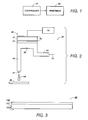
- FIG. 1 is a schematic block diagram of an embodiment of a drop-on-demand drop emitting apparatus.
- FIG. 2 is a schematic block diagram of an embodiment of a drop generator that can be employed in the drop emitting apparatus of FIG. 1 .
- FIG. 3 is a schematic elevational view of an embodiment of an ink jet printhead assembly.
- FIGS. 4A-4G are schematic cross-sectional views of structures that illustrate an embodiment of a procedure for making an array of drop generators.
- FIGS. 5A-5E are schematic cross-sectional views of structures that illustrate another embodiment of a procedure for making an array of drop generators.
- FIG. 1 is a schematic block diagram of an embodiment of a drop-on-demand printing apparatus that includes a controller 10 and a printhead assembly 20 that can include a plurality of drop emitting drop generators.
- the controller 10 selectively energizes the drop generators by providing a respective drive signal to each drop generator.
- Each of the drop generators can employ a piezoelectric transducer.
- FIG. 2 is a schematic block diagram of an embodiment of a drop generator 30 that can be employed in the printhead assembly 20 of the printing apparatus shown in FIG. 1 .
- the drop generator 30 includes an inlet channel 31 that receives ink 33 from a manifold, reservoir or other ink containing structure.
- the ink 33 flows into an ink pressure or pump chamber 35 that is bounded on one side, for example, by a flexible diaphragm 37 .
- a pair of electrodes 43 that receive drop firing and non-firing signals from the controller 10 , and a piezo element 41 disposed therebetween are attached to the flexible diaphragm 37 .
- the electrodes 43 , the piezo element 41 , and the flexible diaphragm 37 can be considered a piezoelectric or electromechanical transducer 39 that is actuated by the controller. If the diaphragm 37 is made of a conductive material, it can comprise an electrode of the piezoelectric transducer 39 . Actuation of the electromechanical transducer 39 causes ink to flow from the pressure chamber 35 through an outlet channel 45 to a drop forming nozzle or orifice 47 , from which an ink drop 49 is emitted toward a receiver medium 48 that can be a transfer surface, for example.
- the piezo element 41 and the electrodes 43 can be considered a driver of the electromechanical transducer.
- the ink 33 can be melted or phase changed solid ink, and the electromechanical transducer 39 can be a piezoelectric transducer that is operated in a bending mode, for example.
- FIG. 3 is a schematic elevational view of an embodiment of an ink jet printhead assembly 20 that can implement a plurality of drop generators 30 ( FIG. 2 ) as an array of drop generators.
- the ink jet printhead assembly includes a fluid channel layer or substructure 131 and a transducer layer or substructure 139 attached to the fluid channel substructure 131 .
- the fluid channel substructure 131 implements fluid channels and portions of chambers of the drop generators 30
- the transducer substructure 139 implements the transducers 39 of the drop generators.
- the nozzles of the drop generators 30 are disposed on an outside surface 131 A of the fluid channel layer 131 that is opposite the diaphragm layer 137 , for example.
- the fluid channel substructure 131 can comprise a laminar stack of plates or sheets, such as stainless steel.
- FIGS. 4A-4G are schematic cross-sectional views of structures being processed that illustrate a procedure for making an array of drop generators.
- a laminar piezoelectric assembly comprising a piezoelectric slab 141 and a relatively thin metal electrode layer 143 is attached to a rigid carrier 111 using double sided tape 113 , wherein the relatively thin metal electrode layer 143 is on the side of the piezoelectric slab 141 attached to the tape.
- a further relatively thin metal electrode layer can optionally be on the other side of the piezoelectric slab 141 .
- the relative thin metal electrode layer or layers can comprise nickel (Ni), for example, and can be formed by a variety of suitable techniques such as vacuum deposition (e.g., sputtering or chemical vapor deposition) or electroless metal plating.
- the piezoelectric assembly is diced or kerfed through the piezoelectric slab 141 and the electrode layer 143 , for example using a dicing saw as is conventional in the semiconductor industry, to form an array of individual electrode/piezo elements, each element comprising a metal electrode 243 and a piezoelectric element 241 .
- the individual piezo elements can alternatively be formed by screen printing, sol gel deposition, or other deposition techniques.
- the array of electrode/piezo elements of the structure of FIG. 4B is then planarized to produce the structure of FIG. 4C .
- the kerf regions between the electrode/piezo elements of the array are filled with a polymer 115 such as epoxy or polyvinyl alcohol.
- the entire array of electrode/piezo elements can optionally be lapped to a desired thickness using conventional lapping or polishing equipment.
- the planarized structure of FIG. 4C is subjected to metal deposition to produce a relatively thick metal layer 237 covering the array of individual electrode/piezo elements as schematically illustrated in FIG. 4D .
- the structure of FIG. 4D generally comprises a plurality of piezoelectric transducers disposed on a carrier substrate, wherein each piezoelectric transducer includes a relatively thick deposited metal diaphragm 237 .
- the deposited metal diaphragm 237 can comprise nickel or chromium, and can be produced by electroless deposition, electroplating, or other deposition techniques such as vacuum deposition (e.g., sputtering or chemical vapor deposition).
- the deposited metal diaphragm layer 237 can have a thickness that is at least about 5 microns, for example in the range of about 5 microns to about 15 microns. As another example, the thickness of the deposited metal layer 237 can be at least about 0.5 to 3 microns. As yet another example, the thickness of the deposited metal layer 237 can be no greater than 30 microns, for example in the range of about 15 microns to about 30 microns.
- the attachment layer 117 is formed on the relatively thick metal diaphragm layer 237 as schematically shown in FIG. 4E .
- the attachment layer 117 can comprise a relatively low temperature solder layer formed by electroplating, for example.
- the attachment layer 117 can comprise a thermoplastic adhesive layer comprising polyimide, epoxy or acrylic adhesive, for example.
- the attachment layer 117 can comprise a thermoplastic layer such as thermoplastic polyimide.
- the attachment layer 117 can also comprise a low temperature glass frit.
- the structure of FIG. 4E can be attached to a fluid channel layer 131 having pressure chambers 35 by reflowing the relatively low temperature solder layer, or by curing the adhesive layer, as appropriate for the particular implementation.
- the carrier 111 and tape 113 are removed to produce the structure of FIG. 4G .
- the planarizing polymer can be left in place, or it can be removed with an appropriate developer, for example.
- FIGS. 5A-5E are schematic cross-sectional views of structures being processed that illustrate a further procedure for making a plurality of drop generators.
- a laminar piezoelectric assembly comprising a piezoelectric slab 141 and a relatively thin metal electrode layer 143 is attached to a rigid carrier using double sided tape 113 , wherein the relatively thin metal electrode layer 143 is on the side of the piezoelectric slab 141 attached to the tape.
- the thin metal electrode layer can comprise deposited nickel.
- the structure of FIG. 5A is subjected to metal deposition to produce a relatively thick metal layer 237 covering the piezoelectric slab 141 , as shown in FIG. 5B .
- the deposited metal layer 237 can comprise nickel or chromium, and can be formed by electroless deposition, electroplating, or other metal deposition methods such as vacuum deposition (e.g., sputtering or chemical vapor deposition).
- the metal layer 237 can have a thickness that is at least about 5 microns, for example in the range of about 5 microns to about 15 microns.
- the thickness of the deposited metal layer 237 can be at least about 0.5 to 3 microns.
- the thickness of the deposited metal layer 237 can be no greater than about 30 microns, for example in the range of about 15 microns to about 30 microns.
- FIG. 5B The structure of FIG. 5B is diced or kerfed through the metal layer 237 , the piezoelectric slab 141 , and the electrode layer 143 using, for example, a dicing saw to produce an array of individual piezoelectric transducers as shown in FIG. 5C , each transducer comprising a thin metal portion 243 , a piezoelectric element 241 and a relatively thick deposited metal portion 337 .
- the structure of FIG. 5C is attached using a suitable adhesive to a metallized polymer diaphragm sub-layer 237 A that is attached to a fluid channel sub-structure 131 having pressure chambers 35 by glue, for example.
- the metallized polymer diaphragm sub-layer 237 A can comprise polyimide, for example.
- the carrier 111 and tape 113 are removed to produce the structure of FIG. 5E wherein the relatively thick deposited metal portions 337 and the metallized polymer diaphragm sub-layer 237 A form the electrodes and diaphragms of the piezoelectric transducers.
- the foregoing can advantageously provide for efficient manufacture of arrays of piezoelectric drop generators, as well as other electromechanical devices.
Abstract
Description
Claims (16)
Priority Applications (2)
| Application Number | Priority Date | Filing Date | Title |
|---|---|---|---|
| US11/635,409 US8006356B2 (en) | 2006-12-07 | 2006-12-07 | Method of forming an array of drop generators |
| US13/195,256 US8397359B2 (en) | 2006-12-07 | 2011-08-01 | Method of manufacturing a drop generator |
Applications Claiming Priority (1)
| Application Number | Priority Date | Filing Date | Title |
|---|---|---|---|
| US11/635,409 US8006356B2 (en) | 2006-12-07 | 2006-12-07 | Method of forming an array of drop generators |
Related Child Applications (1)
| Application Number | Title | Priority Date | Filing Date |
|---|---|---|---|
| US13/195,256 Division US8397359B2 (en) | 2006-12-07 | 2011-08-01 | Method of manufacturing a drop generator |
Publications (2)
| Publication Number | Publication Date |
|---|---|
| US20080138925A1 US20080138925A1 (en) | 2008-06-12 |
| US8006356B2 true US8006356B2 (en) | 2011-08-30 |
Family
ID=39498567
Family Applications (2)
| Application Number | Title | Priority Date | Filing Date |
|---|---|---|---|
| US11/635,409 Active 2029-03-04 US8006356B2 (en) | 2006-12-07 | 2006-12-07 | Method of forming an array of drop generators |
| US13/195,256 Active US8397359B2 (en) | 2006-12-07 | 2011-08-01 | Method of manufacturing a drop generator |
Family Applications After (1)
| Application Number | Title | Priority Date | Filing Date |
|---|---|---|---|
| US13/195,256 Active US8397359B2 (en) | 2006-12-07 | 2011-08-01 | Method of manufacturing a drop generator |
Country Status (1)
| Country | Link |
|---|---|
| US (2) | US8006356B2 (en) |
Cited By (3)
| Publication number | Priority date | Publication date | Assignee | Title |
|---|---|---|---|---|
| US20110141205A1 (en) * | 2009-12-15 | 2011-06-16 | Xerox Corporation | Method of Removing Thermoset Polymer From Piezoelectric Transducers in a Print Head |
| US20110148993A1 (en) * | 2009-12-17 | 2011-06-23 | Xerox Corporation | Inkjet Ejector Having a Polymer Aperture Plate Attached to an Outlet Plate and Method for Assembling an Inkjet Ejector |
| JP2019151074A (en) * | 2018-03-06 | 2019-09-12 | 株式会社リコー | Liquid discharge head, liquid discharge unit, and liquid discharge device |
Families Citing this family (6)
| Publication number | Priority date | Publication date | Assignee | Title |
|---|---|---|---|---|
| US7766463B2 (en) * | 2008-08-19 | 2010-08-03 | Xerox Corporation | Fluid dispensing subassembly with compliant film |
| EP2244489A1 (en) * | 2009-04-24 | 2010-10-27 | Bayer MaterialScience AG | Method for producing an electromechanical converter |
| KR101491802B1 (en) | 2013-05-13 | 2015-02-12 | 알피니언메디칼시스템 주식회사 | Method of manufacturing transducer and transducer manufactured thereby |
| US10166777B2 (en) * | 2016-04-21 | 2019-01-01 | Xerox Corporation | Method of forming piezo driver electrodes |
| JP7187199B2 (en) * | 2018-07-19 | 2022-12-12 | キヤノン株式会社 | METHOD FOR TRANSFERRING MEMBER AND METHOD FOR MANUFACTURING LIQUID EJECTION HEAD |
| EP3651479B1 (en) * | 2018-11-08 | 2022-06-01 | Usound GmbH | Method for producing at least one membrane unit of a mems converter |
Citations (9)
| Publication number | Priority date | Publication date | Assignee | Title |
|---|---|---|---|---|
| US4680595A (en) * | 1985-11-06 | 1987-07-14 | Pitney Bowes Inc. | Impulse ink jet print head and method of making same |
| US5342654A (en) * | 1991-06-19 | 1994-08-30 | Kureha Kagaku Kogyo Kabushiki Kaisha | Surface roughening of resin molded articles for metallizing |
| US5622748A (en) * | 1989-07-11 | 1997-04-22 | Ngk Insulators, Ltd. | Method of fabricating a piezoelectric/electrostrictive actuator |
| US5764596A (en) * | 1994-01-14 | 1998-06-09 | Acounson Corporation | Two-dimensional acoustic array and method for the manufacture thereof |
| JP2001058401A (en) * | 1999-08-20 | 2001-03-06 | Ricoh Co Ltd | Ink-jet head |
| US6341851B1 (en) * | 1996-10-29 | 2002-01-29 | Matsushita Electric Industrial Company, Ltd. | Ink jet recording apparatus including a pressure chamber and pressure applying means |
| US6457222B1 (en) * | 1999-05-28 | 2002-10-01 | Hitachi Koki Co., Ltd. | Method of manufacturing ink jet print head |
| US6557986B2 (en) * | 1999-05-24 | 2003-05-06 | Matsushita Electric Industrial Co., Ltd. | Ink jet head and method for the manufacture thereof |
| US6666943B2 (en) * | 2000-12-04 | 2003-12-23 | Canon Kabushiki Kaisha | Film transfer method |
Family Cites Families (5)
| Publication number | Priority date | Publication date | Assignee | Title |
|---|---|---|---|---|
| JPS5522961A (en) * | 1978-08-07 | 1980-02-19 | Fuji Photo Film Co Ltd | Thermal recording material |
| JPH0397566A (en) * | 1989-09-12 | 1991-04-23 | Brother Ind Ltd | Manufacture of ink jet printing head |
| JPH05169654A (en) * | 1991-12-20 | 1993-07-09 | Seiko Epson Corp | Ink jet recording head and its manufacturing method |
| JP2933608B1 (en) * | 1998-05-14 | 1999-08-16 | 新潟日本電気株式会社 | Ink jet head and method of manufacturing the same |
| US6550691B2 (en) * | 2001-05-22 | 2003-04-22 | Steve Pence | Reagent dispenser head |
-
2006
- 2006-12-07 US US11/635,409 patent/US8006356B2/en active Active
-
2011
- 2011-08-01 US US13/195,256 patent/US8397359B2/en active Active
Patent Citations (9)
| Publication number | Priority date | Publication date | Assignee | Title |
|---|---|---|---|---|
| US4680595A (en) * | 1985-11-06 | 1987-07-14 | Pitney Bowes Inc. | Impulse ink jet print head and method of making same |
| US5622748A (en) * | 1989-07-11 | 1997-04-22 | Ngk Insulators, Ltd. | Method of fabricating a piezoelectric/electrostrictive actuator |
| US5342654A (en) * | 1991-06-19 | 1994-08-30 | Kureha Kagaku Kogyo Kabushiki Kaisha | Surface roughening of resin molded articles for metallizing |
| US5764596A (en) * | 1994-01-14 | 1998-06-09 | Acounson Corporation | Two-dimensional acoustic array and method for the manufacture thereof |
| US6341851B1 (en) * | 1996-10-29 | 2002-01-29 | Matsushita Electric Industrial Company, Ltd. | Ink jet recording apparatus including a pressure chamber and pressure applying means |
| US6557986B2 (en) * | 1999-05-24 | 2003-05-06 | Matsushita Electric Industrial Co., Ltd. | Ink jet head and method for the manufacture thereof |
| US6457222B1 (en) * | 1999-05-28 | 2002-10-01 | Hitachi Koki Co., Ltd. | Method of manufacturing ink jet print head |
| JP2001058401A (en) * | 1999-08-20 | 2001-03-06 | Ricoh Co Ltd | Ink-jet head |
| US6666943B2 (en) * | 2000-12-04 | 2003-12-23 | Canon Kabushiki Kaisha | Film transfer method |
Cited By (9)
| Publication number | Priority date | Publication date | Assignee | Title |
|---|---|---|---|---|
| US20110141205A1 (en) * | 2009-12-15 | 2011-06-16 | Xerox Corporation | Method of Removing Thermoset Polymer From Piezoelectric Transducers in a Print Head |
| US8197037B2 (en) * | 2009-12-15 | 2012-06-12 | Xerox Corporation | Method of removing thermoset polymer from piezoelectric transducers in a print head |
| US20120186739A1 (en) * | 2009-12-15 | 2012-07-26 | Xerox Corporation | Method of Removing Thermoset Polymer From Piezoelectric Transducers in a Print Head |
| US8408683B2 (en) * | 2009-12-15 | 2013-04-02 | Xerox Corporation | Method of removing thermoset polymer from piezoelectric transducers in a print head |
| US20110148993A1 (en) * | 2009-12-17 | 2011-06-23 | Xerox Corporation | Inkjet Ejector Having a Polymer Aperture Plate Attached to an Outlet Plate and Method for Assembling an Inkjet Ejector |
| US8240818B2 (en) * | 2009-12-17 | 2012-08-14 | Xerox Corporation | Inkjet ejector having a polymer aperture plate attached to an outlet plate and method for assembling an inkjet ejector |
| US20120247659A1 (en) * | 2009-12-17 | 2012-10-04 | Xerox Corporation | Method For Assembling A Printhead Having An Inkjet Ejector With A Polymer Aperture Plate Attached To An Outlet Plate |
| US8439486B2 (en) * | 2009-12-17 | 2013-05-14 | Xerox Corporation | Method for assembling a printhead having an inkjet ejector with a polymer aperture plate attached to an outlet plate |
| JP2019151074A (en) * | 2018-03-06 | 2019-09-12 | 株式会社リコー | Liquid discharge head, liquid discharge unit, and liquid discharge device |
Also Published As
| Publication number | Publication date |
|---|---|
| US20110284657A1 (en) | 2011-11-24 |
| US8397359B2 (en) | 2013-03-19 |
| US20080138925A1 (en) | 2008-06-12 |
Similar Documents
| Publication | Publication Date | Title |
|---|---|---|
| US8397359B2 (en) | Method of manufacturing a drop generator | |
| JP5822624B2 (en) | Liquid discharge head and recording apparatus using the same | |
| JP5997150B2 (en) | Liquid discharge head and recording apparatus using the same | |
| CN103561956A (en) | Liquid discharge head and recording device using same | |
| WO2011118833A1 (en) | Drive device for driving fluid discharge head, recording device, and recording method | |
| JPWO2010150876A1 (en) | Liquid discharge head and recording apparatus using the same | |
| US20070120896A1 (en) | Drop generator | |
| JP5893977B2 (en) | Liquid discharge head and recording apparatus using the same | |
| EP1529641B1 (en) | Ink jet apparatus | |
| JP6162504B2 (en) | Liquid discharge head and recording apparatus | |
| US20050045272A1 (en) | Laser removal of adhesive | |
| EP1529642B1 (en) | Ink jet apparatus | |
| JP5388834B2 (en) | Liquid discharge head and recording apparatus using the same | |
| JP2010173135A (en) | Liquid delivery head and recorder using the same | |
| US7143488B2 (en) | Drop emitting apparatus | |
| EP1431035A1 (en) | Ink jet apparatus | |
| WO2016104709A1 (en) | Manufacturing method for liquid-discharging head, liquid-discharging head, and recording device using same | |
| JP6034082B2 (en) | LAMINATE, LIQUID DISCHARGE HEAD AND RECORDING DEVICE USING SAME | |
| US7665828B2 (en) | Drop generator | |
| JP2013244722A (en) | Liquid ejection head and recorder using the same | |
| JP2014046540A (en) | Liquid discharge head and recording device using same |
Legal Events
| Date | Code | Title | Description |
|---|---|---|---|
| AS | Assignment |
Owner name: XEROX CORPORATION, CONNECTICUT Free format text: ASSIGNMENT OF ASSIGNORS INTEREST;ASSIGNORS:ANDREWS, JOHN R.;STEPHENS, TERRANCE L.;REEL/FRAME:018691/0736;SIGNING DATES FROM 20061128 TO 20061129 Owner name: XEROX CORPORATION, CONNECTICUT Free format text: ASSIGNMENT OF ASSIGNORS INTEREST;ASSIGNORS:ANDREWS, JOHN R.;STEPHENS, TERRANCE L.;SIGNING DATES FROM 20061128 TO 20061129;REEL/FRAME:018691/0736 |
|
| FEPP | Fee payment procedure |
Free format text: PAYOR NUMBER ASSIGNED (ORIGINAL EVENT CODE: ASPN); ENTITY STATUS OF PATENT OWNER: LARGE ENTITY |
|
| STCF | Information on status: patent grant |
Free format text: PATENTED CASE |
|
| FPAY | Fee payment |
Year of fee payment: 4 |
|
| MAFP | Maintenance fee payment |
Free format text: PAYMENT OF MAINTENANCE FEE, 8TH YEAR, LARGE ENTITY (ORIGINAL EVENT CODE: M1552); ENTITY STATUS OF PATENT OWNER: LARGE ENTITY Year of fee payment: 8 |
|
| AS | Assignment |
Owner name: CITIBANK, N.A., AS AGENT, DELAWARE Free format text: SECURITY INTEREST;ASSIGNOR:XEROX CORPORATION;REEL/FRAME:062740/0214 Effective date: 20221107 |
|
| MAFP | Maintenance fee payment |
Free format text: PAYMENT OF MAINTENANCE FEE, 12TH YEAR, LARGE ENTITY (ORIGINAL EVENT CODE: M1553); ENTITY STATUS OF PATENT OWNER: LARGE ENTITY Year of fee payment: 12 |
|
| AS | Assignment |
Owner name: XEROX CORPORATION, CONNECTICUT Free format text: RELEASE OF SECURITY INTEREST IN PATENTS AT R/F 062740/0214;ASSIGNOR:CITIBANK, N.A., AS AGENT;REEL/FRAME:063694/0122 Effective date: 20230517 |
|
| AS | Assignment |
Owner name: CITIBANK, N.A., AS COLLATERAL AGENT, NEW YORK Free format text: SECURITY INTEREST;ASSIGNOR:XEROX CORPORATION;REEL/FRAME:064760/0389 Effective date: 20230621 |
|
| AS | Assignment |
Owner name: JEFFERIES FINANCE LLC, AS COLLATERAL AGENT, NEW YORK Free format text: SECURITY INTEREST;ASSIGNOR:XEROX CORPORATION;REEL/FRAME:065628/0019 Effective date: 20231117 |
|
| AS | Assignment |
Owner name: CITIBANK, N.A., AS COLLATERAL AGENT, NEW YORK Free format text: SECURITY INTEREST;ASSIGNOR:XEROX CORPORATION;REEL/FRAME:066741/0001 Effective date: 20240206 |