US8000322B2 - Crossbar switch debugging - Google Patents
Crossbar switch debugging Download PDFInfo
- Publication number
- US8000322B2 US8000322B2 US11/079,414 US7941405A US8000322B2 US 8000322 B2 US8000322 B2 US 8000322B2 US 7941405 A US7941405 A US 7941405A US 8000322 B2 US8000322 B2 US 8000322B2
- Authority
- US
- United States
- Prior art keywords
- port
- debug
- ports
- crossbar
- configuration data
- Prior art date
- Legal status (The legal status is an assumption and is not a legal conclusion. Google has not performed a legal analysis and makes no representation as to the accuracy of the status listed.)
- Active, expires
Links
Images


Classifications
-
- G—PHYSICS
- G06—COMPUTING; CALCULATING OR COUNTING
- G06F—ELECTRIC DIGITAL DATA PROCESSING
- G06F11/00—Error detection; Error correction; Monitoring
- G06F11/22—Detection or location of defective computer hardware by testing during standby operation or during idle time, e.g. start-up testing
- G06F11/2205—Detection or location of defective computer hardware by testing during standby operation or during idle time, e.g. start-up testing using arrangements specific to the hardware being tested
- G06F11/221—Detection or location of defective computer hardware by testing during standby operation or during idle time, e.g. start-up testing using arrangements specific to the hardware being tested to test buses, lines or interfaces, e.g. stuck-at or open line faults
Definitions
- Parallel data transmission consists of sending several bits simultaneously, over separate channels
- serial data transmission consists of sending data bits one at a time over a single channel. While parallel transmission allows for high speed transmission between components that are in close proximity to each other, it is often not conducive to data transmission over longer distances.
- Serial transmission offers several advantages for transmission over longer distances (e.g., lower cost as only one channel is required).
- One technique used to capture the advantages of both data transmission methods is to convert parallel data to serial data for transmission over a channel and then convert the serial data back to parallel data. In order to accomplish this without unduly limiting the transfer rate, a channel with sufficient bandwidth may be used for the data transmission.
- SERDES serial/deserializer
- SERDES serial/deserializer
- Crossbar switches are often used to provide switching in high bandwidth data communication architectures such as SERDES.
- Crossbar switches are used to interconnect devices that are in communication within a computer system.
- the basic function of a crossbar switch is to receive data from one device and route it to another device.
- the crossbar switches are commonly formed on application specific integrated circuits (ASICs).
- ASICs are generally packaged on a chip (e.g., silicon) having a plurality of pins through which connection is made to the elements on the chip.
- testing techniques have been employed to test ASICs at the chip level. These testing techniques typically involve the use of a dedicated debug port formed on the ASIC. Typically, the functionality of the various elements contained on the ASIC is monitored by connecting the output of the dedicated debug port to a monitoring device, such as a logic analyzer.
- a monitoring device such as a logic analyzer.
- this technique has several drawbacks. Because an additional port is required to act as the dedicated debug port, space on the chip is consumed. Additionally, input/output pins are required to be dedicated to the dedicated debug port. After verifying the functionality of the ASIC, the debug port and associated input/output pins are normally not used again, making the debug port an inefficient use of chip resources.
- a crossbar switch having a plurality of ports, such as input/output (I/O) ports.
- a debug process can be performed on the switch using one of the plurality of ports to output chip status information.
- the switch generally uses a debug block to store chip status information.
- the debug block is coupled to a debug bus, which is used to communicate the status information to a selected port where it is output.
- the crossbar switch debug process comprises selecting an output port on the crossbar switch, communicating status information to the selected output port, and outputting the status information via the selected output port.
- the information is output in serial format in accordance with the SERDES protocol.
- FIG. 1 is block diagram illustrating an exemplary computer system upon which one implementation of the current invention can operate.
- FIG. 2 is a block diagram illustrating an application specific integrated circuit (ASIC) containing an 8 port crossbar switch.
- ASIC application specific integrated circuit
- FIG. 3 is a block diagram of an exemplary ASIC containing an 8 port crossbar switch in accordance with one embodiment of the present invention.
- FIG. 4 is a flow chart illustrating the steps of an exemplary process for testing a crossbar switch.
- FIG. 1 an exemplary computing system 100 is shown in which the crossbar switch in accordance with the present invention can operate.
- FIG. 1 illustrates a scalable, partitionable computer system that includes a plurality of elements or cells.
- the cells can be configured to form one or more individual logical or virtual machines, referred to as partitions.
- An example of this type of computing system is the Superdome® system manufactured by Hewlett-Packard (Palo Alto, Calif.).
- each partition contains four cells. It is understood, however, a number of partitions could be contained within the system, limited only by the total number of cells available, and the number of cells each partition contains could range in number from one cell per partition to the total number of cells in the system all contained within a single partition. Each partition is a logical separation from the remainder of the system.
- the first partition 101 a includes four cells 102 a , 102 b , 102 c , 102 d; the second partition 101 b includes four cells 102 e , 102 f , 102 g , 102 h; and the third partition 101 c includes four cells 102 i , 102 j , 102 k, 102 l .
- Partitionable systems such as the system shown in FIG. 1 are typically configured such that each cell within a partition has the ability to communicate with other cells within the same partition, or often with other cells in other partitions.
- crossbar switches 105 a , 105 b , 105 c , 105 d , collectively 105 Communication between partitions and between cells within a partition occurs via one or more crossbar switches 105 a , 105 b , 105 c , 105 d , collectively 105 . Additionally, communication from any particular cell and various other devices on the system (e.g., printers 107 , user interfaces 109 , media drives 111 ) is also done via the crossbar switches 105 .
- the crossbar switches 105 can comprise various number of ports, and are typically formed on ASICs. The relatively complex nature of the computer environment shown in FIG. 1 creates a need to have the ability to verify the performance of the crossbar switches 105 to ensure proper system performance.
- Crossbar switches 105 typically comprise a plurality of input/output ports which are coupled to various devices within the computer environment.
- a conventional 8 port crossbar switch 200 is shown.
- the switch 200 contains eight ports 201 , 202 , 203 , 204 , 205 , 206 , 207 , 208 .
- the switch itself is typically a “smart” switch, meaning the switch can operate to route data in accordance with instructions provided.
- the switch 200 is generally formed on an ASIC 250 .
- the ASIC 250 may also contain a number of register arrays, memory modules, processor cores, etc.
- a single register array 222 is shown for simplicity. It is, however, understood that a number of register arrays may be contained on the ASIC 250 .
- the input/output ports ( 201 - 208 ) are coupled to a debug port 220 .
- This configuration is typically known as a “debug ring.”
- the register array 222 is also coupled to the debug port 220 .
- the debug port 220 is coupled to a plurality of I/O pins on the ASIC 250 .
- a logic analyzer is typically coupled to the I/O pins for the debug port 220 . Special instructions are often used to halt the system operation at a particular point to allow the contents of a register (e.g., register array 222 ) to be read from the debug port 220 .
- Data can be sent from any of the register arrays included on the ASIC 250 or from any of the crossbar ports ( 201 , 202 , 203 , 204 , 205 , 206 , 207 , 208 ) to the debug port 220 , where it is then generally output to a logic analyzer (shown as 325 in FIG. 3 ), typically using a custom designed interface for coupling the logic analyzer to the debug port.
- This technique of debugging ASIC devices, such as crossbar switches requires a dedicated bus path to allow status information to be provided from any register or any port to a plurality of I/O pins. It also requires dedicated I/O pins, as well as an interface to couple a logic analyzer to the I/O pins. All of these items add to chip overhead and reduce available pin resources, which is often a scarce commodity.
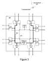
- FIG. 3 shows an exemplary embodiment of an 8-port crossbar switch 300 with debugging capabilities integrated into the existing chip structure using one of the eight existing ports.
- the switch resides on an ASIC and may contain any number of register arrays, memory modules, processor cores, etc., which, for the sake of simplicity, are not shown in FIG. 3 .
- the exemplary crossbar switch 300 comprises eight ports 301 , 302 , 303 , 304 , 305 , 306 , 307 , 308 . Each port is capable of communication with every other port via the crossbar switch interconnect fabric, shown on FIG. 3 as 315 .
- the interconnect fabric 315 is typically a low latency fabric.
- the interconnect fabric 315 permits data received at any one input port to be routed to a desired output port.
- a debug bus 320 resides in the crossbar switch 300 .
- the debug bus 320 typically has a higher latency than the interconnect fabric 315 .
- debug bus 320 is coupled to each of the ports 301 , 302 , 303 , 304 , 305 , 306 , 307 , 308 and also to a debug block 317 .
- Debug block 317 is capable of storing data, and may comprise a register array, an area of random access memory or other similar form of data storage.
- the debug bus 320 allows data to be sent from any of the ports 301 , 302 , 303 , 304 , 305 , 306 , 307 , 308 to the debug block 317 or, additionally, from the debug block 317 to any off-chip location. Data indicating the chip state at any given time or under any particular conditions, referred to as status information, is stored in the debug block 317 .
- the data read from the debug block 317 via the debug bus 320 is communicated via an existing port using the communication protocol under which the crossbar is configured to communicate (e.g., serial communication in accordance with SERDES).
- the communication protocol under which the crossbar is configured to communicate e.g., serial communication in accordance with SERDES.
- one of the plurality of ports is configured to function when desired as a debug port. This is accomplished using a local per-port configuration to instruct a particular port to write to, and read from, the debug bus 320 .
- any port on the crossbar switch 300 can be used to create the debug port.
- the port selected to act as the debug port is unavailable to transmit other data. This results from configuring the port to read from, and write to, the debug bus 320 instead of the switch interconnect fabric 315 .
- the selected port may be reconfigured to act as a typical data port if it is not longer desired to have a debug port, or if it is desired to change the debug port to a different port.
- Port configuration can be accomplished using a control register, for example, control and status register (CSR) 321 , that maintains configuration information for the ports. By writing to the CSR 321 , the selected debug port can be reset to function normally if desired.
- CSR control and status register
- FIG. 4 illustrates the steps involved in performing debug testing on a crossbar switch in accordance with an exemplary implementation of the present invention.
- a port is selected on a crossbar switch to use for debug purposes (step 401 ).
- the selected port is configured using a standard local per-port configuration process to instruct the port to read from the debug bus (step 403 ).
- status information regarding chip operation is stored in a debug block by being sent via the debug bus (step 405 ).
- This information is read via the port selected to act as a debug port (step 407 ).
- the information read via the debug port is can then be analyzed by providing it to a logic analyzer ( 325 in FIG. 3 ) or alternatively by providing the information directly to a processor capable of analyzing the status data.
- the crossbar switch performance is verified during all phases of operation without the need for a resource consuming debug port as used in the prior art.
- an existing port By configuring an existing port to function as a debug port, no additional I/O pins are required, and no additional chip space is required.
- the data retrieved can be output in accordance with existing data transmission protocols (e.g., SERDES), thus enabling it to be transmit/processed in the same manner and at the same bandwidth as functional data.
- existing data transmission protocols e.g., SERDES
Abstract
Description
Claims (14)
Priority Applications (2)
| Application Number | Priority Date | Filing Date | Title |
|---|---|---|---|
| US11/079,414 US8000322B2 (en) | 2004-07-30 | 2005-03-14 | Crossbar switch debugging |
| CN200510088233.2A CN1728105B (en) | 2004-07-30 | 2005-07-29 | Crossbar switch and system including the same |
Applications Claiming Priority (2)
| Application Number | Priority Date | Filing Date | Title |
|---|---|---|---|
| US59247404P | 2004-07-30 | 2004-07-30 | |
| US11/079,414 US8000322B2 (en) | 2004-07-30 | 2005-03-14 | Crossbar switch debugging |
Publications (2)
| Publication Number | Publication Date |
|---|---|
| US20060026468A1 US20060026468A1 (en) | 2006-02-02 |
| US8000322B2 true US8000322B2 (en) | 2011-08-16 |
Family
ID=35733798
Family Applications (1)
| Application Number | Title | Priority Date | Filing Date |
|---|---|---|---|
| US11/079,414 Active 2027-03-14 US8000322B2 (en) | 2004-07-30 | 2005-03-14 | Crossbar switch debugging |
Country Status (2)
| Country | Link |
|---|---|
| US (1) | US8000322B2 (en) |
| CN (1) | CN1728105B (en) |
Cited By (1)
| Publication number | Priority date | Publication date | Assignee | Title |
|---|---|---|---|---|
| US20160162347A1 (en) * | 2014-12-01 | 2016-06-09 | Fujitsu Limited | Information processing apparatus and method of diagnosis |
Families Citing this family (4)
| Publication number | Priority date | Publication date | Assignee | Title |
|---|---|---|---|---|
| US20070024471A1 (en) * | 2005-08-01 | 2007-02-01 | Lexmark International, Inc. | Systems and methods for secure communication over wired transmission channels |
| WO2010083587A1 (en) * | 2009-01-21 | 2010-07-29 | Gennum Corporation | Video specific built-in self test and system test for crosspoint switches |
| CN102214132B (en) * | 2011-05-16 | 2014-07-02 | 曙光信息产业股份有限公司 | Method and device for debugging Loongson central processing unit (CPU), south bridge chip and north bridge chip |
| CN105842615B (en) * | 2015-01-14 | 2019-03-05 | 扬智科技股份有限公司 | The System on Chip/SoC and its adjustment method that can be debugged under abnormality |
Citations (23)
| Publication number | Priority date | Publication date | Assignee | Title |
|---|---|---|---|---|
| US5189665A (en) * | 1989-03-30 | 1993-02-23 | Texas Instruments Incorporated | Programmable configurable digital crossbar switch |
| US5625780A (en) * | 1991-10-30 | 1997-04-29 | I-Cube, Inc. | Programmable backplane for buffering and routing bi-directional signals between terminals of printed circuit boards |
| US5982753A (en) * | 1997-06-09 | 1999-11-09 | Fluke Corporation | Method of testing a switched local area network |
| US6141344A (en) * | 1998-03-19 | 2000-10-31 | 3Com Corporation | Coherence mechanism for distributed address cache in a network switch |
| US6189140B1 (en) * | 1997-04-08 | 2001-02-13 | Advanced Micro Devices, Inc. | Debug interface including logic generating handshake signals between a processor, an input/output port, and a trace logic |
| US20020027908A1 (en) * | 2000-06-19 | 2002-03-07 | Broadcom Corporation | Switch fabric with path redundancy |
| US6445682B1 (en) * | 1998-10-06 | 2002-09-03 | Vertical Networks, Inc. | Systems and methods for multiple mode voice and data communications using intelligently bridged TDM and packet buses and methods for performing telephony and data functions using the same |
| US6587965B1 (en) * | 2000-04-29 | 2003-07-01 | Hewlett-Packard Development Company, L.P. | System and method for single point observability of a dual-mode control interface |
| US6697359B1 (en) * | 1999-07-02 | 2004-02-24 | Ancor Communications, Inc. | High performance switch fabric element and switch systems |
| US6721313B1 (en) * | 2000-08-01 | 2004-04-13 | International Business Machines Corporation | Switch fabric architecture using integrated serdes transceivers |
| US20040085972A1 (en) * | 2002-07-02 | 2004-05-06 | Vixel Corporation | Methods and apparatus for trunking in fibre channel arbitrated loop systems |
| US20040205404A1 (en) * | 2003-03-28 | 2004-10-14 | Johnson Tyler James | Integrated circuit |
| US6850852B1 (en) * | 2000-07-14 | 2005-02-01 | Agilent Technologies, Inc. | System and method for configuring a logic analyzer to trigger on data communications packets and protocols |
| US20050027920A1 (en) * | 2003-07-31 | 2005-02-03 | Fitzsimmons Michael D. | Crossbar switch that supports a multi-port slave device and method of operation |
| US6892248B2 (en) * | 2001-02-21 | 2005-05-10 | International Business Machines Corporation | Method and apparatus for configuring a port on a legacy-free device for general I/O purposes or debugging purposes |
| US20050141429A1 (en) * | 2003-12-29 | 2005-06-30 | Bhaskar Jayakrishnan | Monitoring packet flows |
| US7035228B2 (en) * | 2002-10-29 | 2006-04-25 | Broadcom Corporation | Multi-rate, multi-port, gigabit Serdes transceiver |
| US7051180B2 (en) * | 2002-01-09 | 2006-05-23 | International Business Machines Corporation | Masterless building block binding to partitions using identifiers and indicators |
| US7184916B2 (en) * | 2003-05-20 | 2007-02-27 | Cray Inc. | Apparatus and method for testing memory cards |
| US7200151B2 (en) * | 2002-06-28 | 2007-04-03 | Manter Venitha L | Apparatus and method for arbitrating among equal priority requests |
| US7209476B1 (en) * | 2001-10-12 | 2007-04-24 | Avago Technologies General Ip (Singapore) Pte. Ltd. | Method and apparatus for input/output port mirroring for networking system bring-up and debug |
| US7245587B2 (en) * | 2000-12-20 | 2007-07-17 | Inmon Corporation | Method to associate input and output interfaces with packets read from a mirror port |
| US20090024833A1 (en) * | 1999-09-29 | 2009-01-22 | Silicon Graphics, Inc. | Multiprocessor Node Controller Circuit and Method |
-
2005
- 2005-03-14 US US11/079,414 patent/US8000322B2/en active Active
- 2005-07-29 CN CN200510088233.2A patent/CN1728105B/en active Active
Patent Citations (23)
| Publication number | Priority date | Publication date | Assignee | Title |
|---|---|---|---|---|
| US5189665A (en) * | 1989-03-30 | 1993-02-23 | Texas Instruments Incorporated | Programmable configurable digital crossbar switch |
| US5625780A (en) * | 1991-10-30 | 1997-04-29 | I-Cube, Inc. | Programmable backplane for buffering and routing bi-directional signals between terminals of printed circuit boards |
| US6189140B1 (en) * | 1997-04-08 | 2001-02-13 | Advanced Micro Devices, Inc. | Debug interface including logic generating handshake signals between a processor, an input/output port, and a trace logic |
| US5982753A (en) * | 1997-06-09 | 1999-11-09 | Fluke Corporation | Method of testing a switched local area network |
| US6141344A (en) * | 1998-03-19 | 2000-10-31 | 3Com Corporation | Coherence mechanism for distributed address cache in a network switch |
| US6445682B1 (en) * | 1998-10-06 | 2002-09-03 | Vertical Networks, Inc. | Systems and methods for multiple mode voice and data communications using intelligently bridged TDM and packet buses and methods for performing telephony and data functions using the same |
| US6697359B1 (en) * | 1999-07-02 | 2004-02-24 | Ancor Communications, Inc. | High performance switch fabric element and switch systems |
| US20090024833A1 (en) * | 1999-09-29 | 2009-01-22 | Silicon Graphics, Inc. | Multiprocessor Node Controller Circuit and Method |
| US6587965B1 (en) * | 2000-04-29 | 2003-07-01 | Hewlett-Packard Development Company, L.P. | System and method for single point observability of a dual-mode control interface |
| US20020027908A1 (en) * | 2000-06-19 | 2002-03-07 | Broadcom Corporation | Switch fabric with path redundancy |
| US6850852B1 (en) * | 2000-07-14 | 2005-02-01 | Agilent Technologies, Inc. | System and method for configuring a logic analyzer to trigger on data communications packets and protocols |
| US6721313B1 (en) * | 2000-08-01 | 2004-04-13 | International Business Machines Corporation | Switch fabric architecture using integrated serdes transceivers |
| US7245587B2 (en) * | 2000-12-20 | 2007-07-17 | Inmon Corporation | Method to associate input and output interfaces with packets read from a mirror port |
| US6892248B2 (en) * | 2001-02-21 | 2005-05-10 | International Business Machines Corporation | Method and apparatus for configuring a port on a legacy-free device for general I/O purposes or debugging purposes |
| US7209476B1 (en) * | 2001-10-12 | 2007-04-24 | Avago Technologies General Ip (Singapore) Pte. Ltd. | Method and apparatus for input/output port mirroring for networking system bring-up and debug |
| US7051180B2 (en) * | 2002-01-09 | 2006-05-23 | International Business Machines Corporation | Masterless building block binding to partitions using identifiers and indicators |
| US7200151B2 (en) * | 2002-06-28 | 2007-04-03 | Manter Venitha L | Apparatus and method for arbitrating among equal priority requests |
| US20040085972A1 (en) * | 2002-07-02 | 2004-05-06 | Vixel Corporation | Methods and apparatus for trunking in fibre channel arbitrated loop systems |
| US7035228B2 (en) * | 2002-10-29 | 2006-04-25 | Broadcom Corporation | Multi-rate, multi-port, gigabit Serdes transceiver |
| US20040205404A1 (en) * | 2003-03-28 | 2004-10-14 | Johnson Tyler James | Integrated circuit |
| US7184916B2 (en) * | 2003-05-20 | 2007-02-27 | Cray Inc. | Apparatus and method for testing memory cards |
| US20050027920A1 (en) * | 2003-07-31 | 2005-02-03 | Fitzsimmons Michael D. | Crossbar switch that supports a multi-port slave device and method of operation |
| US20050141429A1 (en) * | 2003-12-29 | 2005-06-30 | Bhaskar Jayakrishnan | Monitoring packet flows |
Cited By (2)
| Publication number | Priority date | Publication date | Assignee | Title |
|---|---|---|---|---|
| US20160162347A1 (en) * | 2014-12-01 | 2016-06-09 | Fujitsu Limited | Information processing apparatus and method of diagnosis |
| US9690647B2 (en) * | 2014-12-01 | 2017-06-27 | Fujitsu Limited | Information processing apparatus and method of diagnosis |
Also Published As
| Publication number | Publication date |
|---|---|
| US20060026468A1 (en) | 2006-02-02 |
| CN1728105A (en) | 2006-02-01 |
| CN1728105B (en) | 2011-01-19 |
Similar Documents
| Publication | Publication Date | Title |
|---|---|---|
| US10243882B1 (en) | Network on chip switch interconnect | |
| US7522468B2 (en) | Serial memory interface | |
| US7096310B2 (en) | Switch configurable for a plurality of communication protocols | |
| US8275579B2 (en) | Communication of a diagnostic signal and a functional signal by an integrated circuit | |
| US8000322B2 (en) | Crossbar switch debugging | |
| US20200409706A1 (en) | Apparatuses and methods involving selective disablement of side effects caused by accessing register sets | |
| US11581056B2 (en) | Apparatuses and methods for direct access hybrid testing | |
| CN112729395A (en) | On-chip sensor reading system for complex SoC reliability monitoring | |
| US7558285B2 (en) | Data processing system and data interfacing method thereof | |
| US7855969B2 (en) | Selective test point for high speed SERDES cores in semiconductor design | |
| US6526535B1 (en) | Synchronous data adaptor | |
| US7543208B2 (en) | JTAG to system bus interface for accessing embedded analysis instruments | |
| US7779197B1 (en) | Device and method for address matching with post matching limit check and nullification | |
| US7647438B1 (en) | Binary base address sorting method and device with shift vector | |
| US7580465B2 (en) | Low speed access to DRAM | |
| US20030193894A1 (en) | Method and apparatus for early zero-credit determination in an infiniband system | |
| US20120137185A1 (en) | Method and apparatus for performing a memory built-in self-test on a plurality of memory element arrays | |
| US11169947B2 (en) | Data transmission system capable of transmitting a great amount of data | |
| US20220190843A1 (en) | Seemingly monolithic interface between separate integrated circuit die | |
| CN103270490B (en) | Network processing unit and the method being connected with external network coprocessor thereof | |
| US7076584B2 (en) | Method and apparatus for interconnecting portions of circuitry within a data processing system | |
| CN114003543B (en) | High-speed serial bus clock compensation method and system | |
| CN115964233B (en) | Interconnection bare chip self-test system and method based on self-test node | |
| US7924845B2 (en) | Message-based low latency circuit emulation signal transfer | |
| George | DESIGN AND READ STABILITYANALYSIS OF 8T SCHMITT TRIGGER BASED SRAMDESIGN OF FIVE PORT PRIORITY BASED ROUTER WITH PORT SELECTION LOGIC FOR NoC |
Legal Events
| Date | Code | Title | Description |
|---|---|---|---|
| AS | Assignment |
Owner name: HEWLETT-PACKARD DEVELOPMENT COMPANY, L.P., TEXAS Free format text: ASSIGNMENT OF ASSIGNORS INTEREST;ASSIGNORS:GREENER, JAMES R.;WOODY, CHRISTOPHER P.;MCFARLAND, ROBERT;AND OTHERS;REEL/FRAME:016390/0595;SIGNING DATES FROM 20050311 TO 20050314 Owner name: HEWLETT-PACKARD DEVELOPMENT COMPANY, L.P., TEXAS Free format text: ASSIGNMENT OF ASSIGNORS INTEREST;ASSIGNORS:GREENER, JAMES R.;WOODY, CHRISTOPHER P.;MCFARLAND, ROBERT;AND OTHERS;SIGNING DATES FROM 20050311 TO 20050314;REEL/FRAME:016390/0595 |
|
| STCF | Information on status: patent grant |
Free format text: PATENTED CASE |
|
| CC | Certificate of correction | ||
| FPAY | Fee payment |
Year of fee payment: 4 |
|
| AS | Assignment |
Owner name: HEWLETT PACKARD ENTERPRISE DEVELOPMENT LP, TEXAS Free format text: ASSIGNMENT OF ASSIGNORS INTEREST;ASSIGNOR:HEWLETT-PACKARD DEVELOPMENT COMPANY, L.P.;REEL/FRAME:037079/0001 Effective date: 20151027 |
|
| MAFP | Maintenance fee payment |
Free format text: PAYMENT OF MAINTENANCE FEE, 8TH YEAR, LARGE ENTITY (ORIGINAL EVENT CODE: M1552); ENTITY STATUS OF PATENT OWNER: LARGE ENTITY Year of fee payment: 8 |
|
| AS | Assignment |
Owner name: OT PATENT ESCROW, LLC, ILLINOIS Free format text: PATENT ASSIGNMENT, SECURITY INTEREST, AND LIEN AGREEMENT;ASSIGNORS:HEWLETT PACKARD ENTERPRISE DEVELOPMENT LP;HEWLETT PACKARD ENTERPRISE COMPANY;REEL/FRAME:055269/0001 Effective date: 20210115 |
|
| AS | Assignment |
Owner name: VALTRUS INNOVATIONS LIMITED, IRELAND Free format text: ASSIGNMENT OF ASSIGNORS INTEREST;ASSIGNOR:OT PATENT ESCROW, LLC;REEL/FRAME:058897/0262 Effective date: 20211102 |
|
| MAFP | Maintenance fee payment |
Free format text: PAYMENT OF MAINTENANCE FEE, 12TH YEAR, LARGE ENTITY (ORIGINAL EVENT CODE: M1553); ENTITY STATUS OF PATENT OWNER: LARGE ENTITY Year of fee payment: 12 |