US7974319B2 - Spectrally tailored pulsed fiber laser oscillator - Google Patents
Spectrally tailored pulsed fiber laser oscillator Download PDFInfo
- Publication number
- US7974319B2 US7974319B2 US12/408,215 US40821509A US7974319B2 US 7974319 B2 US7974319 B2 US 7974319B2 US 40821509 A US40821509 A US 40821509A US 7974319 B2 US7974319 B2 US 7974319B2
- Authority
- US
- United States
- Prior art keywords
- pulse
- fiber laser
- phase
- laser oscillator
- optical pulses
- Prior art date
- Legal status (The legal status is an assumption and is not a legal conclusion. Google has not performed a legal analysis and makes no representation as to the accuracy of the status listed.)
- Active, expires
Links
Images


Classifications
-
- H—ELECTRICITY
- H01—ELECTRIC ELEMENTS
- H01S—DEVICES USING THE PROCESS OF LIGHT AMPLIFICATION BY STIMULATED EMISSION OF RADIATION [LASER] TO AMPLIFY OR GENERATE LIGHT; DEVICES USING STIMULATED EMISSION OF ELECTROMAGNETIC RADIATION IN WAVE RANGES OTHER THAN OPTICAL
- H01S3/00—Lasers, i.e. devices using stimulated emission of electromagnetic radiation in the infrared, visible or ultraviolet wave range
- H01S3/05—Construction or shape of optical resonators; Accommodation of active medium therein; Shape of active medium
- H01S3/06—Construction or shape of active medium
- H01S3/063—Waveguide lasers, i.e. whereby the dimensions of the waveguide are of the order of the light wavelength
- H01S3/067—Fibre lasers
- H01S3/06754—Fibre amplifiers
-
- H—ELECTRICITY
- H01—ELECTRIC ELEMENTS
- H01S—DEVICES USING THE PROCESS OF LIGHT AMPLIFICATION BY STIMULATED EMISSION OF RADIATION [LASER] TO AMPLIFY OR GENERATE LIGHT; DEVICES USING STIMULATED EMISSION OF ELECTROMAGNETIC RADIATION IN WAVE RANGES OTHER THAN OPTICAL
- H01S3/00—Lasers, i.e. devices using stimulated emission of electromagnetic radiation in the infrared, visible or ultraviolet wave range
- H01S3/005—Optical devices external to the laser cavity, specially adapted for lasers, e.g. for homogenisation of the beam or for manipulating laser pulses, e.g. pulse shaping
-
- H—ELECTRICITY
- H01—ELECTRIC ELEMENTS
- H01S—DEVICES USING THE PROCESS OF LIGHT AMPLIFICATION BY STIMULATED EMISSION OF RADIATION [LASER] TO AMPLIFY OR GENERATE LIGHT; DEVICES USING STIMULATED EMISSION OF ELECTROMAGNETIC RADIATION IN WAVE RANGES OTHER THAN OPTICAL
- H01S3/00—Lasers, i.e. devices using stimulated emission of electromagnetic radiation in the infrared, visible or ultraviolet wave range
- H01S3/10—Controlling the intensity, frequency, phase, polarisation or direction of the emitted radiation, e.g. switching, gating, modulating or demodulating
- H01S3/10084—Frequency control by seeding
-
- H—ELECTRICITY
- H01—ELECTRIC ELEMENTS
- H01S—DEVICES USING THE PROCESS OF LIGHT AMPLIFICATION BY STIMULATED EMISSION OF RADIATION [LASER] TO AMPLIFY OR GENERATE LIGHT; DEVICES USING STIMULATED EMISSION OF ELECTROMAGNETIC RADIATION IN WAVE RANGES OTHER THAN OPTICAL
- H01S3/00—Lasers, i.e. devices using stimulated emission of electromagnetic radiation in the infrared, visible or ultraviolet wave range
- H01S3/23—Arrangements of two or more lasers not provided for in groups H01S3/02 - H01S3/22, e.g. tandem arrangements of separate active media
- H01S3/2308—Amplifier arrangements, e.g. MOPA
Definitions
- the present invention relates to the field of laser devices and more particularly concerns methods for tailoring the spectrum of a narrow linewidth pulsed fiber laser.
- High power pulsed fiber laser are currently in demand for a number of applications and uses.
- numerous material processing applications such as memory repair, milling, micro-fabrication, drilling, etc. require pulsed laser systems which provide, among others, the four following characteristics all at the same time and with a great stability over the different conditions of operation and over time:
- the source In other applications such as remote sensing of different chemical species, the source must additionally provide some level of flexibility over the pulse spectrum.
- Scaling the output power without deteriorating other essential characteristics of the laser, such as beam quality or spectral purity, is a main challenge for high power pulsed fiber laser designers.
- SBS Stimulated Brillouin Scattering
- SPM Self-Phase Modulation
- SRS Stimulated Raman Scattering
- SBS threshold the first nonlinear effect that manifests when the pulse peak power exceeds a certain level, the so-called SBS threshold.
- the impacts of SBS are mainly a degradation of the pulse amplitude stability, the appearance of counter-propagating satellite pulses, a roll-off in the laser output power vs pump power curve or even permanent damages to the laser's optical components.
- the process of SBS can be described classically as a parametric interaction among the pump wave (which is formed by the optical pulses), the Stokes wave (partially reflected optical pulses) and an acoustic wave.
- the pump wave generates acoustic waves through electrostriction which in turn causes a periodic modulation of the refractive index in the fiber. This periodic index modulation creates a grating that partially scatters the pump wave through Bragg diffraction, causing the detrimental impacts just described.
- SBS has been studied extensively since its discovery in 1964. For a general presentation of the SBS theory in the context of optical fibers see for example Govind P. Agrawal, “Nonlinear fiber optics”, Academic Press, San Diego, 2001, chapter 9.
- the strain distribution solution is thought to be more adapted to passive single mode fibers in telecom applications but is not considered practical for high power fiber applications, since applying a controlled strain distribution on a LMA fiber while keeping stable beam characteristics is not really attractive from a practical point of view, due to the quite high modal sensitivity to mechanical constraints (torsion, curvatures, etc.) usually displayed by LMA fibers.
- relatively high temperature gradients >100° C. are needed to obtain a valuable SBS threshold increase, which can reduce unacceptably the lifetime and reliability of an LMA fiber incorporating a high index polymer cladding to guide the pump light.
- SBS mitigation schemes include designing a fiber with tailored acoustic properties.
- PAPEN et al. U.S. Pat. No. 6,587,623
- HASEGAWA European patent application no. EP 1 674 901
- HASEGAWA European patent application no. EP 1 674 901
- low-coherence seed sources based on spectrally filtered fluorescence may be used, such as disclosed in international patent application no. WO 2008/086625 (MURISON et al.). Since they do not involve a laser cavity, the fluorescence-based seed sources are not plagued by longitudinal mode beating noise. However, they are relatively inefficient since only a very small fraction of the produced fluorescence (about 0.1% for fiber gain media) is initially selected by the filter element. For polarized sources, the efficiency is even lower as half of the fluorescence power is lost after polarization filtering. Additional optical amplifier stages are therefore often required to boost the output power to usable levels, which increases the overall complexity, component count and cost of the device.
- broad linewidth sources also suffer from a susceptibility to nonlinear effects other than SBS, especially SPM, which may quickly broaden the spectrum beyond the maximum acceptable width as the peak power increases in the fiber amplifier.
- SPM nonlinear effects other than SBS
- This effect is greater for broad linewidth than for narrow linewidth sources, due mainly to the low coherence and to the important phase noise of the former. This transfers the optical power from the spectral region of interest into large spectral “wings”, thereby reducing the spectral power density of the source.
- MURISON et al. disclose a seed source based on a frequency chirp induced by amplitude modulation [see International patent application published under no. WO 2008/086625].
- the chirp is obtained using an amplitude modulator having a non-zero chirp parameter.
- the injection current of a semiconductor laser diode is modulated in order to generate pulses with a frequency chirp along the pulse.
- pulses having triangular shapes are generated and an amplitude modulator located downstream the laser diode further gates the pulse in the time domain.
- the SBS threshold is increased as a result of the spectral broadening corresponding to the frequency chirping.
- amplitude modulation approach for pulsed lasers
- the SBS suppression therefore imposes variable limits or constraints on the pulse shape depending upon the conditions of operation (pulse repetition rate, output power, etc.), limiting the flexibility of the device.
- the chirp creates an additional pulse shape distortion factor for applications using the laser harmonic wavelengths. As the frequency varies more or less linearly along the pulse, the frequency conversion efficiency will also vary along the pulse, leading to pulse shape distortion. Maintaining stable pulse characteristics from laser to laser and over the laser lifetime becomes usually more difficult to achieve as the number of coupled operating parameters increases.
- a pulsed fiber laser oscillator including a light generating module generating optical pulses at a repetition rate. Each optical pulse has a spectral profile, an amplitude profile and a pulse duration.
- the oscillator further includes a spectrum tailoring module for tailoring the spectral profile of the optical pulses.
- the spectrum tailoring module has at least one phase modulator for imposing a time-dependent phase variation on each of the pulses. Synchronizing means are provided for activating the phase modulator in synchronization with the optical pulses.
- a method for providing high power optical pulses while avoiding the onset of non-linear effects comprising:
- FIG. 1 is a schematized representation of a laser system according to an embodiment of the invention.
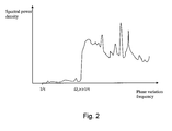
- FIG. 2 is a schematic representation of an example of RF frequency spectrum corresponding to a time-dependent phase variation characterized by a plurality of frequencies.
- FIGS. 3A to 3D are graphs showing the calculated tailored spectra obtained with a single frequency sinusoidal phase variation, for different values of the peak phase deviation.
- FIGS. 4A and 4B are examples of optical spectral profiles obtained respectively with and without modulation of the frequency of the phase variation.
- FIG. 5 is a timing diagram exemplifying the operation of components of an oscillator according to embodiments of the invention.
- FIG. 6 is a graph comparing the peak phase deviation that can be obtained with a given average RF power budget for a synchronously gated sinusoidal phase variation with respect to the case where the phase variation is enabled at all times (CW phase modulation scheme).
- FIG. 7 is a schematized representation of a laser oscillator according to an embodiment of the invention, using a pulsed seed source.
- FIG. 8A is a schematized representation of a laser oscillator using a “MOPA” configuration
- FIG. 8B is a timing diagram for the laser oscillator of FIG. 8A .
- FIG. 9A is a schematized representation of a laser oscillator using a “MOPA” configuration according to another embodiment
- FIG. 9B is a timing diagram for the laser oscillator of FIG. 9A .
- FIG. 10A is a schematized representation of a laser oscillator using a “MOPA” configuration according to yet another embodiment
- FIG. 10B is a timing diagram for the laser oscillator of FIG. 10A .
- FIG. 11A is a schematized representation of a phase modulator driver according to one embodiment of the invention.
- FIG. 11B shows the time variation of the various signals transmitted within the phase modulator driver of FIG. 11A .
- FIG. 12A is a schematized representation of a phase modulator driver according to another embodiment of the invention.
- FIG. 12B shows the time variation of the various signals transmitted within the phase modulator driver of FIG. 12A .
- FIG. 13A is a schematized representation of a phase modulator driver according to another embodiment of the invention.
- FIG. 13B shows the time variation of the various signals transmitted within the phase modulator driver of FIG. 13A .
- FIG. 14A is a schematized representation of a phase modulator driver according to another embodiment of the invention.
- FIG. 14B shows the time variation of the various signals transmitted within the phase modulator driver of FIG. 14A .
- FIG. 15A to 15C are schematized representations of phase modulator drivers using a plurality of source elements according to embodiments of the invention.
- FIG. 16A is a schematic representation of a laser oscillator according to an embodiment of the invention, using a double-pass configuration.
- FIG. 16B is a timing diagram for the embodiment of FIG. 16A .
- FIG. 17 is a graph showing the experimental comparison of spectral broadening obtained using a single pass vs a double pass configuration.
- FIG. 18 is a schematic representation of a laser oscillator according to an embodiment of the invention, using a plurality of phase modulators with associated drivers and synchronization means.
- FIG. 19 is a schematic representation of a laser oscillator according to an embodiment of the invention, using a plurality of phase modulators with associated drivers and synchronization means, in a double-pass configuration.
- FIG. 20 is a graph showing the SBS threshold dependence on the pulse duration.
- FIG. 21 is a graph of experimental result showing SBS suppression for a pulsed fiber laser.
- FIG. 22 is a graph of experimental result showing SBS suppression, where the output pulse energy can be increased by a factor of ten at least when using a synchronously gated phase variation scheme.
- FIG. 23 is a graph of experimental spectra obtained at different output pulse energy levels.
- FIG. 24 is a graph of experimental results showing that most of the energy can be maintained in a narrow spectral bandwidth while scaling the output power.
- FIG. 25A is a graph of calculated spectra showing an example of the impact of SPM for a seed based on filtered ASE
- FIG. 25B is a graph of calculated spectra showing an example of the impact of SPM for a seed based on a narrow linewidth laser diode and a synchronously gated phase variation scheme
- FIG. 25C shows a superposition of the spectra of FIGS. 25A and 25B to compare the impact of SPM for the two associated types of seed sources.
- FIG. 26 is a graph comparing the effect of SPM on the spectral linewidth of pulsed fiber lasers as a function of the output energy per pulse for a seed source based on filtered ASE with respect to a seed source based on a narrow linewidth, phase modulated laser.
- FIG. 27 is an example of spectral width control enhancement provided by a synchronously gated phase variation scheme.
- FIG. 28 is an example of SPM-induced spectral broadening slope as a function of the source linewidth.
- FIG. 29 is an example of a synchronously gated phase variation signal used to impose a linear frequency chirp along the optical pulse.
- Embodiments of the present invention generally provide pulse generating methods and pulsed fiber laser oscillators for laser systems adapted for high power applications such as memory repair, milling, micro-fabrication, drilling and other material processing applications. It will be understood that embodiments of the present invention may also be used in other contexts such as remote sensing or any other application which may benefit from high power pulses having good optical characteristics.
- oscillator is understood to refer to the portion of a laser system which generates light pulses.
- the oscillator may include a laser cavity or alternatively be based on fluorescent emissions.
- the oscillator may be part of a larger system including amplifying, beam shaping or any other optical component further defining the properties of the optical pulses generated by the oscillator.
- the laser oscillators according to embodiments of the present invention are preferably fiber-based, which is understood to mean that light circulating in the oscillator is generally guided by optical fiber. It is however not excluded from the scope of the invention that the oscillator may include components external to optical fibers. In addition, the components of the laser oscillator may be embodied in more than one length of optical fiber, coupled together through known techniques such as fiber pigtails, fused coupling, mechanical couplers and the like.
- the optical fiber or fibers embodying each components of the laser oscillator may have any appropriate structure. Depending on its function the optical fiber may be single mode or multimode, with a single or multiple cladding. It may be embodied by a standard fiber, a polarisation maintaining (PM) fiber, a microstructured (or “holey”) fiber or any other appropriate specialized type of fiber. It may be made of any suitable materials such as pure silica, doped silica, composite glasses or sapphire.
- the oscillator 22 first includes a light generating module 24 , which generates optical pulses 26 .
- the light generating module 24 determines the characteristics of the optical pulses 26 outputted thereby such as their repetition rate, pulse duration, spectral profile and amplitude profile.
- the light generating module 24 includes a seed assembly 28 generating the optical pulses 26 and a pulse generator 30 collaborating with the seed assembly 28 to control the pulse characteristics.
- the laser oscillator 22 further includes a spectrum tailoring module 42 for tailoring the spectral profile of the optical pulses 26 generated by the light generating module 24 .
- the spectrum tailoring module 42 includes a phase modulator 44 which imposes a time-dependent phase variation on each optical pulse 26 therethrough.
- a phase modulator driver 48 drives the activation of the phase modulator 44 through a phase variation drive signal 50 providing the desired phase variation.
- the spectrum tailoring module imposes a phase component on the electrical field of the optical pulses which is not constant over the duration of each pulse.
- the time-dependent phase variation may be periodic, quasi-periodic, linear or have any other appropriate time-dependence.
- the phase variation drive signal 50 is a RF signal characterised by one or more frequencies in the range of 100 MHz to 100 GHz.
- FIG. 2 illustrates the general case of an RF spectrum corresponding to a phase variation drive signal having a plurality (in this case a continuum) of frequencies.
- the phase modulator 44 may be embodied by an electro-optic component based modulator such as well known in the art.
- the electro-optical material included in the phase modulator can be LiNbO 3 , LiTaO 3 , KNbO 3 or any other appropriate nonlinear material.
- the phase modulator may be based on an acousto-optical component such as an acousto-optic modulator.
- the spectrum tailoring module 42 may include more than one phase modulator 44 in a cascade, each applying a phase variation to the optical pulses therethrough so that their combined effect on the phase of the optical pulses results in the desired tailoring of their spectral profile.
- the spectrum tailoring module 42 may be configured so that the light pulses make more than one pass through one of more phase modulator 44 , as will be explained further below with respect to the embodiments of FIGS. 16A and 19 .
- each optical pulse 26 At the input of the phase modulator 44 each optical pulse 26 generally has a spectral profile centered at an optical frequency ⁇ with a linewidth ⁇ .
- additional spectral components can be added to the pulse spectral profile under certain conditions specific to the characteristics of the pulse and of the phase variation, thereby broadening the pulse spectral profile.
- E ( t ) E 0 sin(2 ⁇ v ⁇ t + ⁇ ( t )) (1) where ⁇ (t) is the time-dependent phase term that varies when applying the phase variation.
- the peak phase deviation obtained when applying a peak voltage V peak on the phase modulator 44 is given by:
- ⁇ peak ⁇ ⁇ V peak V ⁇ ( 3 )
- V ⁇ is a characteristic of the phase modulator 44 .
- the Fourier decomposition of E(t) with ⁇ (t) given by equation (2) is a well known result of applied mathematics (see for example Bruce Carlson, “Communication systems—An introduction to Signals and Noise in Electrical Communication”, McGraw-Hill, New York, 1986, chapter 7).
- ⁇ n ⁇ an integer
- n> ⁇ peak the spectral power density decreases rapidly as n increases.
- Typical spectral profiles of the optical pulses after tailoring are shown in FIGS. 3A to 3D , for various values of ⁇ peak and a same value of ⁇ . It can be easily understood that by simply choosing appropriate values for both parameters of the phase variation, ⁇ and ⁇ peak , tailoring of the spectral profile of the optical pulses is readily achieved.
- the resulting spectral profile of the optical pulses may be uniform along the pulse. This may be achieved by ensuring that the spectrum tailoring takes place within a duration significantly shorter than the pulse duration. This will be the case if the condition ⁇ >>1/ ⁇ is satisfied, where ⁇ is the pulse duration. For example, for 10 ns pulses this condition corresponds to ⁇ >>100 MHz, and ideally for such pulses ⁇ is of the order of at least 1 GHz.
- phase variation frequency may further be advantageous in embodiments where the initial phase of the phase variation with respect to the optical pulse leading edge is not kept fixed or not controlled (parameter ⁇ 0 in equation (2)).
- the optical frequency sweep provided by the phase variation will in general vary differently along the pulse from pulse to pulse, which could lead to a situation where the spectral characteristics of the pulse can change significantly from pulse to pulse in an uncontrolled manner.
- the phase variation may differ from the simple oscillatory case described above, providing an even greater versatility in the spectrum tailoring capacities of the device.
- the profile of the phase variation may be adapted in view of the requirements of the application to which the laser oscillator is destined.
- the phase variation signal ⁇ (t) spectrum can be considered to include a spectrum of n discrete frequencies ⁇ 1 , ⁇ 2 , ⁇ 3 , . . . , ⁇ n or a continuum of frequencies.
- the phase variation preferably has a spectrum of frequencies having a lower cut-off frequency ⁇ c significantly larger than 1/ ⁇ .
- An example of such an RF spectrum is illustrated in FIG. 2 .
- ⁇ 0 is the central phase variation frequency
- speak is the maximum deviation of ⁇ with respect to ⁇ 0
- ⁇ is the frequency at which the phase modulation frequency is varied.
- FIG. 4B shows an example of spectral profile which can be obtained with this scheme, compared to the corresponding case where the phase variation frequency is fixed as shown in FIG. 4A .
- the modulation of the phase variation frequency allows for the distribution of the optical power among many additional spectral components with respect to the fixed phase variation frequency case, which reduces the maximum spectral power density, shown on the vertical axis, for a fixed spectral band.
- Such a reduction can be advantageously used for mitigating SBS in high power fiber amplifiers.
- the pulsed laser oscillator 22 further includes means for synchronizing the activation of the phase modulator 44 with the arrival of the optical pulses 26 thereat.
- This synchronization is an advantageous aspect of the present invention as it allows for using low average power RF amplifiers to drive the phase modulators and limits the thermal stress on the phase modulators, which is beneficial in terms of system cost, complexity and reliability, as will be explained below.
- the synchronizing means are conceptually represented by the arrow 46 extending between the pulse generator 30 and the phase modulator driver 48 and one skilled in the art will understand that any combination of components and signals allowing the control of the timing of the activation of the phase modulator 44 in relation to the propagation of the optical pulses 26 therethrough could be used without departing from the scope of the present invention.
- phase modulation 44 is activated to the “on” state while an optical pulse 26 propagates therethrough and is kept in the “off” state during inter-pulse period.
- the expression “synchronously gated phase variation” is used herein to refer to this regime of operation.
- a conceptual timing diagram is represented in FIG. 5 for a laser operating at a pulse repetition rate PRR.
- the phase modulation drive signal is enabled synchronously with the optical pulse for a duration approximately equal to the pulse duration ⁇ .
- the delay ⁇ is in general dependent upon the optical pulse propagation delay between the seed assembly 28 and the phase modulator 44 and also depends upon the electrical propagation delays between the pulse generator 30 , the seed assembly 28 and the phase modulator driver 48 .
- the delay ⁇ is adjusted in order to make sure that the phase variation is active while an optical pulse is transmitted through the phase modulator and not active otherwise.
- the duty cycle is only 0.1%, which mean that the phase modulator 44 can be advantageously kept in the “off” state for up to 99.9% of the time using this method.
- the phase modulator is activated synchronously with the optical pulses for a delay that is slightly longer than the pulse duration so as to provide a security margin with respect to the possible variations associated to jitter or to other time-related tolerances.
- the phase modulator can be driven synchronously with the optical pulses for a duration approximately equal to ⁇ max , this duration being kept constant for any chosen pulse duration.
- the duration of the phase variation can be set to be approximately equal to the optical pulse duration over the whole range ⁇ min to ⁇ max , which means that it is adjusted accordingly every time the optical pulse duration is modified.
- the initial phase of the phase modulation signal with respect to the optical pulse leading edge can be controlled or not. All of these variants and equivalents thereof are considered activations of the phase modulator “in synchronization” with the optical pulses.
- the synchronously gated phase variation scheme considerably reduces the RF average power level required for efficiently tailoring the pulse spectral profile, as the phase modulation is active for only a small fraction of time with respect to a continuous wave phase modulation scheme (phase modulation active at all times).
- This much lower RF power consumption is advantageous in terms of cost and reliability.
- the power dissipated in the phase modulator can be considerably reduced (three orders of magnitude reduction in the example mentioned above), which significantly mitigates the risk of experiencing thermal issues with the device.
- the required RF power is much lower than it is in the CW regime, much higher peak phase deviations can be obtained with a given amount of average RF power, thereby allowing broader spectra and more efficient SBS suppression.
- the synchronously gated phase variation scheme is compared with the CW phase modulation scheme in terms of the peak phase deviation (which is proportional to the spectral broadening) that can be achieved as a function of the available RF average power budget.
- the synchronously gated time-dependent phase variation authorizes much broader spectra when compared with the CW scheme for a given RF power budget. For example, a modest RF power budget of 10 dBm is sufficient to enable a peak phase deviation as large as 11 ⁇ with the synchronously gated regime, whereas it is limited to about 0.4 ⁇ in the CW regime.
- the tailoring of the spectral profile of the optical pulses may be accomplished by controlling the phase variation parameters from pulse to pulse using high speed electronics embodying the pulse generator, phase modulator driver and other related components.
- a suitable platform is for example disclosed in U.S. provisional patent application No. 61/076337 by Deladurantaye P. et al., filed on 27 Jun. 2008 and entitled “Embedded digital laser pulse shaping platform and method”.
- the phase variation characteristics as well as the pulse amplitude profile are both dynamically controlled from pulse to pulse, thereby allowing the production of extremely flexible and agile pulsed fiber lasers in both the time domain and the optical frequency domain. Examples of such embodiments are presented below.
- the pulse seed source 32 may be a semiconductor laser diode of any appropriate configuration such as a Fabry-Perot cavity, a distributed-feedback diode, an external-cavity diode laser (ECDL), etc.
- the semiconductor diode may be fiber-based and guide light in a single mode in a transverse or longitudinal regime.
- the pulse generator 30 may for example be embodied by a device or platform apt to generate a pulse drive signal 36 of appropriate characteristics, and is preferably based on high speed electronics. In the embodiment of FIG.
- the drive signal 36 should be tailored to vary the drive current of the pulsed seed source 32 in order for the optical pulses 26 generated thereby to have the desired shape.
- the optical characteristics of the optical pulses 26 will depend on a number of factors such as the complex impedance of the pulsed seed source 32 , which is itself dependent on the physics of the cavity of this source and on the diode package.
- FIGS. 8A and 9A show alternative embodiments where the seed assembly 28 includes a continuous light source 36 generating a continuous light beam 38 , followed by first and second amplitude modulators 40 a , 40 b modulating the continuous light beam 38 to provide the optical pulses 26 .
- the pulse generator 30 sends a first drive signal 34 a to a first amplitude modulator 40 a which is external to the continuous seed light source 36 , and the first drive signal 34 a controls the opening of the first amplitude modulator 40 to allow light therethrough according to the desired output shape of the optical pulses 26 formed in this manner.
- a second drive signal 34 b is provided to a second amplitude modulator 40 b to open the same in complete or partial synchronization with the arrival of the optical pulses 26 thereat, providing a greater resolution and versatility in the characteristics of the resulting pulses.
- a second amplitude modulator 40 b is provided to open the same in complete or partial synchronization with the arrival of the optical pulses 26 thereat, providing a greater resolution and versatility in the characteristics of the resulting pulses.
- both amplitude modulators 40 a and 40 b are positioned upstream the spectrum tailoring module 42 , and an optical amplifier 52 is placed in between.
- the amplifier may for example be embodied by a pumped gain medium such as a rare-earth doped length of optical fiber.
- FIG. 9A shows an other embodiment, where the spectrum tailoring module 42 is positioned upstream both modulators 40 a and 40 b .
- the synchronously gated regime is made possible by driving the spectrum tailoring module 42 first and then synchronizing the two amplitude modulators 40 a and 40 b in order to generate and shape optical pulses 26 in synchronicity with the time windows for which the continuous light beam phase has been varied by the spectrum tailoring module 42 .
- An optical amplifier 52 may also be provided in those embodiments.
- FIGS. 8B , 9 B and 10 B illustrate examples of timing diagrams corresponding to the embodiments of FIGS. 8A , 9 A and 10 A respectively.
- either type of seed source whether pulsed 32 or continuous 36 may be tunable in wavelength, according to techniques known in the art.
- external spectral tuning components such as filters, gratings or the like (not shown) may be provided externally to the seed source.
- the phase modulator driver preferably includes a source module which generates a source signal and a high speed switching module which selectively transmits this source signal from the source module to the phase modulator.
- the high speed switching module is activated by the pulse synchronization signal.
- a variable gain amplifying module is also preferably provided and disposed between the high speed switching module and the phase modulator.
- the three modules of the phase modulator driver 48 may be embodied by an oscillator 64 , a variable gain amplifier 68 and a high-speed switch 66 .
- the source signal provided by the oscillator 64 is an oscillating signal 70 at a fixed frequency which defines the frequency ⁇ of the phase variation drive signal 50 .
- the phase variation peak amplitude can be adjusted by controlling the gain of the amplifier 68 , which may advantageously also be activated synchronously with the optical pulses as shown in the timing diagram of FIG. 11B . In terms of RF spectrum as represented in FIG. 2 , this case corresponds to the case of a single peak of frequency ⁇ with variable intensity from pulse to pulse.
- the high speed switch 66 is preferably activated by the pulse synchronization signal 46 so as to selectively transmit the oscillating signal 70 through the amplifier 68 to the phase modulator 44 only when an optical pulse is present at its input, in order to minimize the RF power consumption of the device as explained above.
- the pulse to pulse spectrum tailoring capability is exemplified for two consecutive pulses 26 A and 26 B.
- both pulses 26 A and 26 B Before entering the spectrum tailoring module 42 , both pulses 26 A and 26 B have an identical spectral profile (or spectrum) X.
- the gain of the amplifier 68 may be controlled by a gain signal 72 .
- the gain signal 72 sets the gain of the amplifier 68 to two different values for the time windows corresponding to pulses 26 A and 26 B, respectively, the gain being set to a lower value for pulse 26 B with respect to pulse 26 A. Consequently, the phase modulator 44 is driven with a higher phase variation peak amplitude for pulse 26 A than for pulse 26 B, resulting in a more important peak phase deviation for pulse 26 A than for pulse 26 B.
- the spectrum Y obtained for pulse 26 A is broader than the spectrum Z of pulse 26 B, as the broadening is approximately proportional to the peak phase deviation, as can be seen in FIGS. 3A o 3 D.
- both pulses also have different spectral profiles in general, as also shown in FIGS. 3A through 3D .
- FIG. 12A shows an alternative embodiment of FIG. 11A where the synchronized gain control signal of the RF amplifier has tailored characteristics in the time domain.
- the amplitude profile of this signal is tailored in a different manner for two consecutive pulses. Consequently, the amplitude of the phase variation can be varied differently along each pulse using this scheme, which corresponds to different pulse spectral profiles having variable spectral linewidths along each pulse.
- the optical pulse A is characterized by a broader linewidth at the beginning of the pulse and a narrower linewidth at the end of the pulse.
- optical pulse B has a narrower linewidth at the beginning of the pulse and a broader linewidth at the end of the pulse.
- various time-dependent spectral profiles can be produced along the optical pulses, and from pulse to pulse.
- very flexible pulsed fiber oscillators offering both tailored pulse shapes and tailored pulse spectra can be produced.
- phase modulation driver 48 where the source module is embodied by a noise source 74 generating a noise signal 76 having a variable frequency and defining a more complex phase variation frequency profile, as for example illustrated in FIG. 2 .
- the corresponding timing diagram is shown at FIG. 13B .
- This embodiment could be useful for SBS suppression or for applications where a broad (or “white”) optical spectrum is desirable, for example in some spectroscopic remote sensing applications where one or several chemical species are to be detected in a given spectral bandwidth, each specie having its own set of spectral absorption bands.
- phase modulator driver architectures can be employed in order to generate different RF spectra, for example by combining several oscillators and/or several RF amplifiers, without departing from the scope of the present invention. Examples of such architectures are presented in FIGS. 15A to 15C .
- FIG. 14A illustrates an alternative embodiment that can also provide optical pulses with spectral characteristics that vary along the pulses.
- source module is embodied by a voltage-controlled oscillator (VCO) 80 .
- VCO 80 is a single frequency oscillator whose frequency can be controlled with a voltage over a certain range.
- An example of VCO is the model ZX95-1200W+ (trademark) from Mini-Circuits of Brooklyn, N.Y.
- the VCO frequency is controlled with a tailored control signal 82 , in synchronization with the optical pulses.
- the RF amplifier gain is controlled as in FIG. 12A . Using this configuration, both the frequency and the amplitude of the phase variation can be tailored along each pulse.
- the timing diagram for this embodiment is shown in FIG. 14B .
- FIGS. 15A to 15C show alternative embodiments where the source module includes a plurality of source elements such as oscillators 64 , having one or possibly different frequencies, VCOs 80 and noise sources 74 . Each source element generates a corresponding source signal component. Of course, any appropriate number of source elements may be provided, in any appropriate combination depending on the desired end result.
- a combiner 84 is preferably provided to combine the source signal components from each source element into the source signal. In the embodiment of FIG. 15A , the combiner positioned directly downstream the source elements, therefore combining their output before the switching module. In the embodiment of FIG.
- the switching module includes a plurality of high speed switches, each associated with a corresponding source element, and the combiner is provided between the switching module and the gain amplifying module.
- the embodiment of FIG. 15C shows a variant where the gain amplifying module also includes individual gain amplifiers in series with a corresponding source element and high speed switch chain, the combiner being provided downstream the gain amplifying module.
- the spectrum tailoring module 42 includes a recirculation assembly recirculating the optical pulses 26 through the phase modulator 44 for a plurality of passes.
- a circulator 54 and a reflective element 56 are used for this purpose.
- the optical pulses 26 impinge on a first port 58 of the circulator and exit the same through a second port 60 in communication with the phase modulator 44 .
- a first pass of the optical pulses 26 through the phase modulator 44 tailors their spectral profile a first time.
- the tailored optical pulses are then reflected by the reflective element 56 , for example a fiber Bragg grating, located downstream the phase modulator 44 and connected to its output.
- the reflected pulses 26 then traverse the phase modulator 44 for a second time where their spectral profile is further tailored, re-enter the second port 60 of the circulator 54 and are finally outputted at a third port 62 of the circulator 54 .
- the phase variation drive signal 50 is synchronized with the optical pulses 26 so that the phase modulator 44 is active only while an optical pulse is transmitted through the phase modulator 44 in either direction.
- FIG. 16B shows an example of corresponding timing diagram.
- the embodiment of FIG. 16A provides in principle a twofold increase of the spectral broadening factor with respect to single-pass schemes for the same phase variation condition.
- a 3 dB reduction in the RF average power required to drive the phase modulator is possible in principle.
- the achievable improvement is dependent upon the phase modulator design, the optical path length and other practical limitations. For example, phase shifts occurring during the pulse propagation must be compensated. This can be done by a fine tuning of the phase modulation frequency.
- FIG. 17 presents experimental results comparing the double pass scheme with respect to the single pass configuration. Although not as important as the theoretically predicted value because of the experimental setup limitations, some improvement in the RF power budget was obtained.
- FIG. 18 there is shown an embodiment where a plurality of phase modulators 44 are provided in series, each having an associated phase modulator driver 48 .
- a pulse synchronization signal is transmitted to each phase modulator driver, taking into account the appropriate propagation delays.
- Each phase modulator may impose a same time-dependent phase variation on the light therethrough, or different phase variation components may be combined to obtain the desired phase at the output of the spectrum tailoring module 42 .
- FIG. 19 shows an alternative embodiment combining some of the features of the embodiments of FIGS. 16A and 18 , providing a reflective element 56 and the end of a cascade of phase modulators 44 so that the optical pulses 26 are modulated by each phase modulator twice.
- optical pulses is understood to refer to pulses having a peak power which is sufficient for typical material processing and sensing applications as explained above.
- a pulse energy of at least 50 ⁇ J is considered “high power”, although this value is given as a general indication and is not considered limitative to the scope of the invention.
- the methods taught can also be applied to limit the onset and the impact of SBS and SPM in low average power fiber oscillators comprising single mode fibers with mode field diameters of a few microns. As a matter of fact, the methods can be applied as soon as the intensity of the pulses in the fiber core reaches the non linear effects intensity threshold, independent of the fiber mode field diameter.
- the method first includes generating seed optical pulses, for example with a light generating assembly according to one of the embodiments described above or equivalents thereof.
- the spectral profile of these seed pulses is then broadened by propagation through at least one phase modulator imposing a time-dependent phase variation on each of these seed pulses.
- the phase modulator is activated in synchronization with the seed optical pulses therethrough.
- the optical pulses are amplified, thereby obtaining the high power optical pulses. It will be understood that any of the above described embodiments of the oscillator or equivalents thereof may be used to realize the method generally described herein.
- Embodiments of the method described above may provide a powerful tool for overcoming the SBS limitations affecting other narrow linewidth, high power fiber lasers while not sacrificing the beam quality, the flexibility, the stability and the reliability of the lasers.
- the SBS suppression efficiency provided by phase modulation in the field of high power pulsed fiber lasers is dependent upon two main factors. The first one is the maximum achievable spectral broadening, which is governed by the frequency spectrum of the phase variation and by the peak phase deviation. The second one is the phase modulation dynamics with respect to the SBS dynamics in the context of pulses having durations of the same order of magnitude than the lifetime of the SBS phonon.
- the SBS gain is reduced by a factor 1+ ⁇ signal / ⁇ B that depends on the ratio of the signal linewidth ⁇ signal to the Brillouin-gain bandwidth ⁇ B with respect to the maximum Brillouin gain obtained for a very narrow linewidth signal (see for example Cotter, D. “ Stimulated Brillouin Scattering in Monomode Optical Fiber ”, J. Opt. Commun. 4 (1983) 1, 10-19).
- ⁇ B is of the order of 50-100 MHz in optical fibers at a wavelength of 1 ⁇ m.
- the SBS threshold is generally dependent upon the relative values of the pulse duration and of the phonon lifetime, as predicted by transient SBS models (see Boyd, R. W., “ Nonlinear Optics ”, Academic Press, 2003, pp. 427-428)
- FIG. 20 shows experimental results demonstrating that the SBS threshold varies with the pulse duration.
- SBS can be suppressed using a synchronously gated, time-dependent phase variation through the broadening of the spectral profile of the optical pulses.
- ⁇ signal obtained with phase variation at a frequency ⁇
- a duration 1/ ⁇ is required to sweep the complete optical frequency span. For durations shorter than 1/ ⁇ the average linewidth is therefore smaller than ⁇ signal .
- FIG. 21 shows an example of SBS suppression obtained experimentally for a pulse duration of 10 ns.
- FIG. 22 presents another experimental example of SBS suppression.
- the LMA fiber amplifier maximum output pulse energy is clearly limited at 12 ⁇ J without a phase variation, as the backward signal intensity increases exponentially beyond this threshold.
- the amplified pulse spectral profile remains quite narrow, as can be see in FIG. 23 , an important characteristic for applications involving frequency conversion.
- FIG. 24 where the energy per pulse emitted in a spectral bandwidth of 0.5 nm is plotted against the injected pump power in the LMA fiber pump core.
- the slight broadening of the spectrum is the result of the onset of SPM, which also means that SBS no longer represents a concern.
- SPM mitigation is the subject of the next section.
- FIG. 25A shows an example of calculated spectra with broadening caused by SPM for a seed based on filtered ASE, whereas FIG.
- FIG. 25B presents the calculated broadening for a phase-modulated narrow linewidth single longitudinal-mode seed.
- SPM broadens the spectrum considerably, as the final spectral width is about ten times larger than the initial linewidth.
- each of the individual spectral lines is slightly broadened by SPM and the energy remains in the initial spectral envelope.
- FIG. 25C compares the spectra of FIGS. 25A and 25B using the same horizontal scale, to emphasize the different magnitudes of the spectral broadening induced by SPM for both types of seeds.
- FIG. 26 shows a typical example of how SPM affects the spectral width of the output pulses as a function of their energy.
- the pulses are amplified in 2.5m of LMA fiber.
- the spectral width of the pulses in the case of a 500 pm wide filtered ASE source.
- a phase modulated source is characterized by a spectral width, which corresponds to the width of the total envelope, and a single peak linewidth, which is the linewidth of the source before the time-dependent phase variation is applied.
- FIG. 28 A numerical comparison of the spectral broadening slope predicted for a filtered ASE source and for a phase modulated filtered ASE source is presented in FIG. 28 as a function of the source linewidth, considering the same length of the same LMA fiber employed to generate the graph of FIG. 26 .
- the linewidth appearing on the horizontal axis of the graph of FIG. 28 corresponds to the spectral width of the source itself, not the spectral width of the envelope generated by the phase modulation. It is clear from those results that the broader the source is, the more it will be affected by SPM through spectral broadening.
- a phase modulated source can have a significantly broader initial spectral width (see FIG.
- the spectral bandwidth of the amplified optical pulses remains of the order of 500 pm for output energy levels as high as 150 ⁇ J, as shown in FIG. 26 .
- the second option is superior to the first one as it yields optical pulses with high energy levels and narrow spectral linewidths simultaneously.
- some embodiments of the present invention can efficiently scale the peak power of high power pulsed fiber lasers and mitigate both SBS and SPM.
- a seed source having a linewidth that is as narrow as possible such as a very coherent single longitudinal mode semiconductor laser diode. It may also be advantageous to use the phase modulation techniques disclosed with respect to embodiments of the present invention to add optical frequencies so as to broaden the spectral envelope of the seed by a factor that is just sufficient to suppress SBS.
- the pulse to pulse spectral agility of some embodiments of the present invention is particularly well adapted to remote sensing applications such as Differential Absorption LIDAR (DIAL) and range-resolved Tunable Diode Laser Spectroscopy (TDLS). Both techniques are used to measure the concentration of gas or air-suspended particles, and require complex laser sources for illuminating the target, whose absorption or scattering is measured as a function of laser wavelength. DIAL requires a source with two emission wavelengths and measures the differential absorption loss at the two wavelengths due to the gas or particles. The differential measurement allows for higher sensitivity than standard LIDAR. TDLS instead uses a tuneable laser source and measures a spectrum of absorption or scattering by illuminating the target and sweeping the laser wavelength.
- DIAL Differential Absorption LIDAR
- TDLS range-resolved Tunable Diode Laser Spectroscopy
- Embodiments of the present invention can provide high peak power laser sources with very narrow linewidths by choosing a suitable seed. Moreover, the laser output power or pulse energy can be significantly increased with minimum alteration of the spectrum over previously disclosed fibre based laser sources because the SBS threshold is increased and the SPM is controlled very well.
- Both DIAL and TDLS can be implemented using embodiments of the present invention. For example, in the case of TDLS, a linear frequency chirp along the optical pulse can be imposed and controlled from pulse to pulse, which corresponds to a quadratic increase of the optical phase along the pulse for the phase variation signal, followed by a phase reset between two pulses, as illustrated in FIG.
Abstract
Description
-
- High pulse energy (50 μJ or higher) with excellent pulse amplitude stability, for processing material at the laser operating wavelength or for efficient frequency conversion;
- Excellent beam quality (M2<1.1, astigmatism <10%, beam roundness >95%) with robust single mode operation, for superior processing quality, high throughput processes and efficient frequency conversion;
- Narrow linewidth (Δλ<0.5 nm), for small spot sizes and efficient frequency conversion; and
- Great flexibility in terms of control of the pulse temporal profile, like pulse to pulse control over the temporal profile at high (>100 kHz) repetition rates.
-
- a) generating seed optical pulses at a repetition rate, each seed optical pulse having a spectral profile, an amplitude profile and a pulse duration;
- b) broadening the spectral profile of the seed optical pulses, said broadening comprising propagating the seed optical pulses through at least one phase modulator imposing a time-dependent phase variation on each of said pulses, thereby obtaining spectrally broadened optical pulses, said broadening comprising activating the phase modulator in synchronization with the seed optical pulses; and
- c) amplifying said broadened optical pulses, thereby obtaining said high power optical pulses.
E(t)=E 0 sin(2τv×t+φ(t)) (1)
where φ(t) is the time-dependent phase term that varies when applying the phase variation. In the single frequency example, this term has the profile:
φ(t)=φpeak sin(2τΩ×t+φ 0) (2)
where φ0 is the initial phase and φpeak the peak phase deviation. The peak phase deviation obtained when applying a peak voltage Vpeak on the
where Vπ is a characteristic of the
φ(t)=φpeak sin(2τ(Ω0+Ωpeak sin(2τΨt))×t+φ 0) (4)
where Ω0 is the central phase variation frequency, speak is the maximum deviation of Ω with respect to Ω0 and Ψ is the frequency at which the phase modulation frequency is varied.
Synchronously Gated Phase Variation
Claims (30)
Priority Applications (4)
| Application Number | Priority Date | Filing Date | Title |
|---|---|---|---|
| US12/408,215 US7974319B2 (en) | 2008-11-21 | 2009-03-20 | Spectrally tailored pulsed fiber laser oscillator |
| CA2743373A CA2743373C (en) | 2008-11-21 | 2009-11-23 | Device and method for generating bursts of picosecond optical sub-pulses |
| US12/624,324 US8798107B2 (en) | 2008-11-21 | 2009-11-23 | Device and method for generating bursts of picosecond optical sub-pulses |
| PCT/CA2009/001692 WO2010057314A1 (en) | 2008-11-21 | 2009-11-23 | Device and method for generating bursts of picosecond optical sub-pulses |
Applications Claiming Priority (2)
| Application Number | Priority Date | Filing Date | Title |
|---|---|---|---|
| US11687308P | 2008-11-21 | 2008-11-21 | |
| US12/408,215 US7974319B2 (en) | 2008-11-21 | 2009-03-20 | Spectrally tailored pulsed fiber laser oscillator |
Related Child Applications (2)
| Application Number | Title | Priority Date | Filing Date |
|---|---|---|---|
| US12/624,324 Continuation US8798107B2 (en) | 2008-11-21 | 2009-11-23 | Device and method for generating bursts of picosecond optical sub-pulses |
| US12/624,324 Continuation-In-Part US8798107B2 (en) | 2008-11-21 | 2009-11-23 | Device and method for generating bursts of picosecond optical sub-pulses |
Publications (2)
| Publication Number | Publication Date |
|---|---|
| US20100128744A1 US20100128744A1 (en) | 2010-05-27 |
| US7974319B2 true US7974319B2 (en) | 2011-07-05 |
Family
ID=42196218
Family Applications (2)
| Application Number | Title | Priority Date | Filing Date |
|---|---|---|---|
| US12/408,215 Active 2030-01-26 US7974319B2 (en) | 2008-11-21 | 2009-03-20 | Spectrally tailored pulsed fiber laser oscillator |
| US12/624,324 Active 2032-07-15 US8798107B2 (en) | 2008-11-21 | 2009-11-23 | Device and method for generating bursts of picosecond optical sub-pulses |
Family Applications After (1)
| Application Number | Title | Priority Date | Filing Date |
|---|---|---|---|
| US12/624,324 Active 2032-07-15 US8798107B2 (en) | 2008-11-21 | 2009-11-23 | Device and method for generating bursts of picosecond optical sub-pulses |
Country Status (3)
| Country | Link |
|---|---|
| US (2) | US7974319B2 (en) |
| CA (2) | CA2743648C (en) |
| WO (2) | WO2010057290A1 (en) |
Cited By (5)
| Publication number | Priority date | Publication date | Assignee | Title |
|---|---|---|---|---|
| US20110262144A1 (en) * | 2010-04-21 | 2011-10-27 | Brian Ishaug | Compensation of distortion from SBS/IIN suppression modulation |
| US20120163833A1 (en) * | 2010-12-22 | 2012-06-28 | General Instrument Corporation | System and method for reducing mutual leakage between distributed feedback laser and electro-absorption modulator in integrated electro-absorption modulated laser |
| US20130242380A1 (en) * | 2012-03-16 | 2013-09-19 | Kla-Tencor Corporation | Suppression Of Parasitic Optical Feedback In Pulse Laser Systems |
| US9036252B1 (en) | 2014-09-11 | 2015-05-19 | Northrop Grumman Systems Corporation | Nonlinear spectrally narrowed fiber amplifier |
| US10390883B2 (en) | 2014-05-28 | 2019-08-27 | Institut National D'optique | Laser-directed microcavitation |
Families Citing this family (55)
| Publication number | Priority date | Publication date | Assignee | Title |
|---|---|---|---|---|
| EP2175569B1 (en) * | 2008-10-07 | 2013-09-25 | Universität Ulm | Transmission device for creating an analog modulated pulse train and for transmitting the same and reception device for receiving a corresponding signal |
| US7974319B2 (en) * | 2008-11-21 | 2011-07-05 | Institut National D'optique | Spectrally tailored pulsed fiber laser oscillator |
| US20110170564A1 (en) * | 2009-12-21 | 2011-07-14 | Institut National D'optique | Fiber laser oscillators and systems using an optimized phase varying function |
| WO2011075851A1 (en) * | 2009-12-23 | 2011-06-30 | Institut National D'optique | System and method for the spatial tailoring of laser light using temporal phase modulation |
| US8263903B2 (en) | 2010-05-18 | 2012-09-11 | Institut National D'optique | Method for stablizing an output of a pulsed laser system using pulse shaping |
| CN101950913A (en) * | 2010-08-12 | 2011-01-19 | 上海拜安实业有限公司 | Fiber laser source based on pulse seed source amplification and fiber sensing system |
| KR101145683B1 (en) * | 2010-10-13 | 2012-05-24 | 광주과학기술원 | Method of oscillating burst mode in laser system and apparatus for the same |
| US8411716B2 (en) | 2011-01-26 | 2013-04-02 | Institut National D'optique | Circuit assembly for controlling an optical system to generate optical pulses and pulse bursts |
| US9166355B2 (en) * | 2011-09-12 | 2015-10-20 | Lawrence Livermore National Security, Llc | Directly driven source of multi-gigahertz, sub-picosecond optical pulses |
| JP5962669B2 (en) * | 2012-01-13 | 2016-08-03 | 住友大阪セメント株式会社 | Optical pulse generator and chirp compensation method of optical pulse generator |
| US9590385B2 (en) * | 2012-07-18 | 2017-03-07 | Cubic Corporation | Compact laser source |
| US8937976B2 (en) | 2012-08-15 | 2015-01-20 | Northrop Grumman Systems Corp. | Tunable system for generating an optical pulse based on a double-pass semiconductor optical amplifier |
| US10260990B2 (en) * | 2013-06-12 | 2019-04-16 | Corning Incorporated | Multi-wavelength DMD measurement apparatus and methods |
| DE102013108583A1 (en) * | 2013-08-08 | 2015-03-05 | Osram Opto Semiconductors Gmbh | Method for separating a composite into semiconductor chips and semiconductor chip |
| US9913688B1 (en) * | 2013-10-01 | 2018-03-13 | Cutera, Inc. | Split pulse picosecond laser for tattoo removal |
| US10928659B2 (en) | 2014-02-24 | 2021-02-23 | Rockley Photonics Limited | Optoelectronic device |
| KR20150145803A (en) * | 2014-06-19 | 2015-12-31 | 한국전자통신연구원 | Apparatus and method for generating pulse laser |
| KR102439093B1 (en) * | 2014-07-03 | 2022-08-31 | 아이피지 포토닉스 코포레이션 | Process and system for uniformly recrystallizing amorphous silicon substrate by fiber laser |
| CN104332809B (en) * | 2014-08-25 | 2015-08-26 | 深圳市创鑫激光股份有限公司 | Based on the adjustable pulse width pulse optical fiber of acoustooptic switch |
| CN104201550A (en) * | 2014-08-27 | 2014-12-10 | 广东高聚激光有限公司 | Picosecond pulse fibre laser and pulse generation method thereof |
| US10921616B2 (en) | 2016-11-23 | 2021-02-16 | Rockley Photonics Limited | Optoelectronic device |
| US11150494B2 (en) | 2015-03-05 | 2021-10-19 | Rockley Photonics Limited | Waveguide modulator structures |
| US10557939B2 (en) | 2015-10-19 | 2020-02-11 | Luminar Technologies, Inc. | Lidar system with improved signal-to-noise ratio in the presence of solar background noise |
| WO2017079483A1 (en) | 2015-11-05 | 2017-05-11 | Luminar Technologies, Inc. | Lidar system with improved scanning speed for high-resolution depth mapping |
| WO2017095817A1 (en) | 2015-11-30 | 2017-06-08 | Luminar Technologies, Inc. | Lidar system with distributed laser and multiple sensor heads and pulsed laser for lidar system |
| CN105390919A (en) * | 2015-12-03 | 2016-03-09 | 哈尔滨工业大学 | Method for obtaining high-repetition-frequency large-energy tunable laser |
| CN105305214A (en) * | 2015-12-03 | 2016-02-03 | 哈尔滨工业大学 | Method for acquiring high repetition frequency and large energy ultraviolet tunable laser pulses |
| US10135542B2 (en) * | 2016-12-15 | 2018-11-20 | Rockley Photonics Limited | Optical modulators |
| US11101256B2 (en) | 2016-11-23 | 2021-08-24 | Rockley Photonics Limited | Optical modulators |
| US11105975B2 (en) | 2016-12-02 | 2021-08-31 | Rockley Photonics Limited | Waveguide optoelectronic device |
| US11036006B2 (en) | 2016-12-02 | 2021-06-15 | Rockley Photonics Limited | Waveguide device and method of doping a waveguide device |
| US9871339B1 (en) | 2016-12-15 | 2018-01-16 | Raytheon Company | Laser transmitter for generating a coherent laser output signal with reduced self-phase modulation and method |
| US9905992B1 (en) | 2017-03-16 | 2018-02-27 | Luminar Technologies, Inc. | Self-Raman laser for lidar system |
| US9810786B1 (en) | 2017-03-16 | 2017-11-07 | Luminar Technologies, Inc. | Optical parametric oscillator for lidar system |
| US9810775B1 (en) | 2017-03-16 | 2017-11-07 | Luminar Technologies, Inc. | Q-switched laser for LIDAR system |
| US9869754B1 (en) | 2017-03-22 | 2018-01-16 | Luminar Technologies, Inc. | Scan patterns for lidar systems |
| US10007001B1 (en) | 2017-03-28 | 2018-06-26 | Luminar Technologies, Inc. | Active short-wave infrared four-dimensional camera |
| US10545240B2 (en) | 2017-03-28 | 2020-01-28 | Luminar Technologies, Inc. | LIDAR transmitter and detector system using pulse encoding to reduce range ambiguity |
| WO2018217780A1 (en) | 2017-05-23 | 2018-11-29 | Thorlabs, Inc. | Sinusoidal phase modulation of mode-lock lasers |
| US11070020B2 (en) * | 2017-05-23 | 2021-07-20 | Thorlabs, Inc. | Sinusoidal phase modulation of mode-locked lasers |
| US10985519B2 (en) | 2017-06-21 | 2021-04-20 | Institut National D'optique | Active LMA optical fiber and laser system using the same |
| US10811837B2 (en) * | 2017-12-18 | 2020-10-20 | Northrop Grumman Systems Corporation | AM/FM seed for nonlinear spectrally compressed fiber amplifier |
| FR3081737B1 (en) * | 2018-06-05 | 2022-02-11 | Imagine Optic | METHODS AND SYSTEMS FOR THE GENERATION OF HIGH CRETE POWER LASER PULSES |
| FR3081738B1 (en) * | 2018-06-05 | 2020-09-04 | Imagine Optic | METHODS AND SYSTEMS FOR THE GENERATION OF LASER PULSES OF HIGH PEAK POWER |
| DE102018006137A1 (en) * | 2018-08-03 | 2020-02-06 | Paragon Gmbh & Co. Kgaa | Particle measuring device and method for determining the particle mass concentrations in aerosols |
| US11411366B2 (en) * | 2019-01-15 | 2022-08-09 | Northrop Grumman Systems Corporation | Combined laser architecture using wavelength multiplexed seed source |
| US11757248B2 (en) * | 2019-07-19 | 2023-09-12 | Raytheon Company | System and method for spectral line shape optimization for spectral beam combining of fiber lasers |
| US10802120B1 (en) * | 2019-08-20 | 2020-10-13 | Luminar Technologies, Inc. | Coherent pulsed lidar system |
| CN113474953A (en) * | 2019-09-20 | 2021-10-01 | 统雷有限公司 | Sinusoidal phase modulation for mode-locked lasers |
| US11546058B1 (en) * | 2020-01-29 | 2023-01-03 | Cable Television Laboratories, Inc. | Systems and methods for chromatic dispersion pre-compensation |
| US11539441B1 (en) * | 2020-01-29 | 2022-12-27 | Cable Television Laboratories, Inc. | Chirp-compensating transmitter and method |
| US11495934B1 (en) * | 2020-05-13 | 2022-11-08 | University Of Central Florida Research Foundation, Inc. | Tailored laser pulse trains for burst-mode illumination |
| CN111780856B (en) * | 2020-06-01 | 2022-03-29 | 哈尔滨工业大学 | Optical fiber distributed vibration measurement method based on Rayleigh scattering spectrum phase spectrum analysis |
| US20220043202A1 (en) | 2020-08-10 | 2022-02-10 | Luminar, Llc | Semiconductor optical amplifier with bragg grating |
| US20220120900A1 (en) * | 2020-10-15 | 2022-04-21 | Waymo Llc | Light detection and ranging device using combined pulse and continuous optical signals |
Citations (27)
| Publication number | Priority date | Publication date | Assignee | Title |
|---|---|---|---|---|
| US4560246A (en) | 1982-06-04 | 1985-12-24 | British Telecommunications | Optical transmission |
| US5200964A (en) | 1991-03-12 | 1993-04-06 | General Instrument Corporation | Broad linewidth lasers for optical fiber communication systems |
| US5432631A (en) | 1994-04-06 | 1995-07-11 | At&T Corp. | Dual-wavelength source of high-repetition rate, transform-limited optical pulses |
| US5566381A (en) | 1995-03-02 | 1996-10-15 | Lucent Technologies Inc. | Multifrequency lightwave source using phase modulation for suppressing stimulated brillouin scattering in optical fibers |
| US5930024A (en) | 1996-10-23 | 1999-07-27 | Scientific-Atlanta, Inc. | Suppression of stimulated Brillouin scattering in optical transmission system |
| US6072615A (en) | 1997-06-13 | 2000-06-06 | Lucent Technologies Inc. | Phase modulator-based generation of high-quality high bit rate return-to-zero optical data streams |
| US6108465A (en) | 1997-10-14 | 2000-08-22 | Ando Electric Co., Ltd. | Optical pulse generator |
| US6151338A (en) | 1997-02-19 | 2000-11-21 | Sdl, Inc. | High power laser optical amplifier system |
| US20020003641A1 (en) * | 2000-05-08 | 2002-01-10 | Hall Katherine L. | Polarization division multiplexer |
| US6552301B2 (en) | 2000-01-25 | 2003-04-22 | Peter R. Herman | Burst-ultrafast laser machining method |
| US6587623B1 (en) | 2000-08-14 | 2003-07-01 | The Board Of Trustees Of The University Of Illinois | Method for reducing stimulated brillouin scattering in waveguide systems and devices |
| US6778565B2 (en) | 2001-09-24 | 2004-08-17 | Gigatera Ag | Pulse-generating laser |
| US6813448B1 (en) | 2000-07-28 | 2004-11-02 | Adc Telecommunications, Inc. | Suppression of stimulated brillouin scattering in optical transmissions |
| US6856640B2 (en) | 2000-10-23 | 2005-02-15 | Lumera Laser Gmbh | Device for producing laser light |
| US20060018349A1 (en) | 2004-07-14 | 2006-01-26 | High Q Laser Production Gmbh | Pulse train generator and method for generating a repeating sequence of laser pulses |
| EP1674901A1 (en) | 2004-12-27 | 2006-06-28 | Sumitomo Electric Industries, Ltd. | Optical fiber with reduced stimulated Brillouin scattering |
| US20060159138A1 (en) | 2004-12-21 | 2006-07-20 | Institut National D'optique | Pulsed laser light source |
| US7103285B1 (en) | 1999-04-13 | 2006-09-05 | Sumitomo Electric Industries, Ltd. | Optical transmission system for reducing nonlinear optical phenomena using modulation depth control system |
| US20060245456A1 (en) | 2005-04-28 | 2006-11-02 | Precision Photonics Corporation | Systems and methods for generating high repetition rate ultra-short optical pulses |
| US20070196048A1 (en) | 2006-01-12 | 2007-08-23 | Almantas Galvanauskas | Optical waveform shaping |
| WO2007118333A1 (en) | 2006-04-19 | 2007-10-25 | Pyrophotonics Lasers, Inc. | Method and system for a high power low- coherence pulsed light source |
| WO2008032021A2 (en) | 2006-09-11 | 2008-03-20 | Qinetiq Limited | Optical clock |
| US7349637B1 (en) | 2003-02-11 | 2008-03-25 | Optium Corporation | Optical transmitter with SBS suppression |
| WO2008086625A1 (en) | 2007-01-18 | 2008-07-24 | Pyrophotonics Lasers Inc. | Seed source for high power optical fiber amplifier |
| US7428253B2 (en) | 2006-09-29 | 2008-09-23 | Pyrophotonics Lasers Inc. | Method and system for a pulsed laser source emitting shaped optical waveforms |
| US20090323741A1 (en) | 2008-06-27 | 2009-12-31 | Institut National D'optique | Digital laser pulse shaping module and system |
| US20100135347A1 (en) | 2008-11-21 | 2010-06-03 | Institut National D'optique | Device and method for generating bursts of picosecond optical sub-pulses |
Family Cites Families (2)
| Publication number | Priority date | Publication date | Assignee | Title |
|---|---|---|---|---|
| US5200972A (en) * | 1991-06-17 | 1993-04-06 | The United States Of America As Represented By The Secretary Of The Navy | ND laser with co-doped ion(s) pumped by visible laser diodes |
| US5619364A (en) * | 1995-02-22 | 1997-04-08 | The United States Of America As Represented By The Secretary Of The Navy | Depolarized source for high power operation of an integrated optical modulator |
-
2009
- 2009-03-20 US US12/408,215 patent/US7974319B2/en active Active
- 2009-03-20 WO PCT/CA2009/000365 patent/WO2010057290A1/en active Application Filing
- 2009-03-20 CA CA2743648A patent/CA2743648C/en active Active
- 2009-11-23 US US12/624,324 patent/US8798107B2/en active Active
- 2009-11-23 CA CA2743373A patent/CA2743373C/en active Active
- 2009-11-23 WO PCT/CA2009/001692 patent/WO2010057314A1/en active Application Filing
Patent Citations (28)
| Publication number | Priority date | Publication date | Assignee | Title |
|---|---|---|---|---|
| US4560246B1 (en) | 1982-06-04 | 1998-06-09 | British Telecomm | Optical transmission |
| US4560246A (en) | 1982-06-04 | 1985-12-24 | British Telecommunications | Optical transmission |
| US5200964A (en) | 1991-03-12 | 1993-04-06 | General Instrument Corporation | Broad linewidth lasers for optical fiber communication systems |
| US5432631A (en) | 1994-04-06 | 1995-07-11 | At&T Corp. | Dual-wavelength source of high-repetition rate, transform-limited optical pulses |
| US5566381A (en) | 1995-03-02 | 1996-10-15 | Lucent Technologies Inc. | Multifrequency lightwave source using phase modulation for suppressing stimulated brillouin scattering in optical fibers |
| US5930024A (en) | 1996-10-23 | 1999-07-27 | Scientific-Atlanta, Inc. | Suppression of stimulated Brillouin scattering in optical transmission system |
| US6151338A (en) | 1997-02-19 | 2000-11-21 | Sdl, Inc. | High power laser optical amplifier system |
| US6072615A (en) | 1997-06-13 | 2000-06-06 | Lucent Technologies Inc. | Phase modulator-based generation of high-quality high bit rate return-to-zero optical data streams |
| US6108465A (en) | 1997-10-14 | 2000-08-22 | Ando Electric Co., Ltd. | Optical pulse generator |
| US7103285B1 (en) | 1999-04-13 | 2006-09-05 | Sumitomo Electric Industries, Ltd. | Optical transmission system for reducing nonlinear optical phenomena using modulation depth control system |
| US6552301B2 (en) | 2000-01-25 | 2003-04-22 | Peter R. Herman | Burst-ultrafast laser machining method |
| US20020003641A1 (en) * | 2000-05-08 | 2002-01-10 | Hall Katherine L. | Polarization division multiplexer |
| US6813448B1 (en) | 2000-07-28 | 2004-11-02 | Adc Telecommunications, Inc. | Suppression of stimulated brillouin scattering in optical transmissions |
| US6587623B1 (en) | 2000-08-14 | 2003-07-01 | The Board Of Trustees Of The University Of Illinois | Method for reducing stimulated brillouin scattering in waveguide systems and devices |
| US6856640B2 (en) | 2000-10-23 | 2005-02-15 | Lumera Laser Gmbh | Device for producing laser light |
| US6778565B2 (en) | 2001-09-24 | 2004-08-17 | Gigatera Ag | Pulse-generating laser |
| US7349637B1 (en) | 2003-02-11 | 2008-03-25 | Optium Corporation | Optical transmitter with SBS suppression |
| US20060018349A1 (en) | 2004-07-14 | 2006-01-26 | High Q Laser Production Gmbh | Pulse train generator and method for generating a repeating sequence of laser pulses |
| US20060159138A1 (en) | 2004-12-21 | 2006-07-20 | Institut National D'optique | Pulsed laser light source |
| EP1674901A1 (en) | 2004-12-27 | 2006-06-28 | Sumitomo Electric Industries, Ltd. | Optical fiber with reduced stimulated Brillouin scattering |
| US20060245456A1 (en) | 2005-04-28 | 2006-11-02 | Precision Photonics Corporation | Systems and methods for generating high repetition rate ultra-short optical pulses |
| US20070196048A1 (en) | 2006-01-12 | 2007-08-23 | Almantas Galvanauskas | Optical waveform shaping |
| WO2007118333A1 (en) | 2006-04-19 | 2007-10-25 | Pyrophotonics Lasers, Inc. | Method and system for a high power low- coherence pulsed light source |
| WO2008032021A2 (en) | 2006-09-11 | 2008-03-20 | Qinetiq Limited | Optical clock |
| US7428253B2 (en) | 2006-09-29 | 2008-09-23 | Pyrophotonics Lasers Inc. | Method and system for a pulsed laser source emitting shaped optical waveforms |
| WO2008086625A1 (en) | 2007-01-18 | 2008-07-24 | Pyrophotonics Lasers Inc. | Seed source for high power optical fiber amplifier |
| US20090323741A1 (en) | 2008-06-27 | 2009-12-31 | Institut National D'optique | Digital laser pulse shaping module and system |
| US20100135347A1 (en) | 2008-11-21 | 2010-06-03 | Institut National D'optique | Device and method for generating bursts of picosecond optical sub-pulses |
Non-Patent Citations (15)
| Title |
|---|
| Agrawal, Govind P. Nonlinear Fiber Optics. Academic Press, San Diego, 2001. Chapter 9, pp. 370-403. |
| Boggio et al. "8 dB increase of the SBS threshold in an optical fiber by applying a stair ramp strain distribution." Conference on Lasers and electro-Optics/International Quantum Electronics Conference and Photonic Applications Systems Technologies. Technical Digest (CD) Optical Society of America, 2004, paper CThT30. |
| Boyd, R.W. Nonlinear Optics. 3rd Edition, Academic Press, 2008, Section 9.3.3., pp. 447-448. |
| Boyd, R.W. Nonlinear Optics. 3rd Edition, Academic Press, 2008, Section 9.3.3., pp. 447-448. |
| Cotter et al. "Stimulated Brillouin Scattering in Monomode Optical Fiber." Journal of Optical Communications, vol. 4, Issue 1, 1983, pp. 10-19. |
| Forrester et al. "Effects of heat transfer and energy absorption in the ablation of biological tissues by pulsetrainburst (.100 MHz) ultrafast laser processing", Photonics North, 2006, Proc. Of SPIE, vol. 6343, 63430J-I. |
| Golovchenko, E. et al. "Analysis of optical pulse train generation through filtering of an externally phase-modulated signal from a CW laser", Electronics Letters, vol. 31, No. 16, Aug. 1995, pp. 1364-1366. |
| Hansryd et al. "Increase of the SBS Threshold ina Short Highly Nonlinear Fiber by Applying a Temperature Distribution." Journal of Lightwave Technology. vol. 19, No. 11, Nov. 2001, pp. 1691-1697. |
| International Preliminary Report on Patentability for International Patent Application Serial No. PCT/CA2009/000365 dated Nov. 15, 2010. |
| International Search Report for International Patent Application Serial No. PCT/CA2009/001692 mailed Feb. 8, 2010. |
| Jiang et al. "Optical Processing Based on Spectral Line-by-Line Pulse Shaping on a Phase-Modulated CW Laser", IEEE Journal of Quantum Elecronics, vol. 42, No. 7, Jul. 2006, pp. 657-666. |
| Jiang, Z. et al. "Optical arbitrary waveform processing of more than 100 spectral comb lines", Nature Photonics, vol. 1, Aug. 2007, pp. 463-467. |
| Mamyshev "Dual-wavelength source of high-repetition-rate, transform-limited optical pulses for soliton transmission", Optics Letters, vol. 19, No. 24, Dec. 15, 1994, pp. 2074-2076. |
| Nebel et al. "Generation of tailored picosecond-pulse-trains for micro-machining", Photonics West 2006, LASE Conference: Commercial and biomedical Applications of Ultrafast Lasers VI, Paper No. 6108-37 1/8. |
| Yamada et al. "Application of planar lightwave circuit platform to hybrid integrated optical WDM transmitter/receiver module", IEEE Electronics Letters Online, 19950941 (1995). |
Cited By (8)
| Publication number | Priority date | Publication date | Assignee | Title |
|---|---|---|---|---|
| US20110262144A1 (en) * | 2010-04-21 | 2011-10-27 | Brian Ishaug | Compensation of distortion from SBS/IIN suppression modulation |
| US9865989B2 (en) * | 2010-04-21 | 2018-01-09 | Arris Enterprises Llc | Compensation of distortion from SBS/IIN suppression modulation |
| US20120163833A1 (en) * | 2010-12-22 | 2012-06-28 | General Instrument Corporation | System and method for reducing mutual leakage between distributed feedback laser and electro-absorption modulator in integrated electro-absorption modulated laser |
| US8509626B2 (en) * | 2010-12-22 | 2013-08-13 | General Instrument Corporation | System and method for reducing mutual leakage between distributed feedback laser and electro-absorption modulator in integrated electro-absorption modulated laser |
| US20130242380A1 (en) * | 2012-03-16 | 2013-09-19 | Kla-Tencor Corporation | Suppression Of Parasitic Optical Feedback In Pulse Laser Systems |
| US8767291B2 (en) * | 2012-03-16 | 2014-07-01 | Kla-Tencor Corporation | Suppression of parasitic optical feedback in pulse laser systems |
| US10390883B2 (en) | 2014-05-28 | 2019-08-27 | Institut National D'optique | Laser-directed microcavitation |
| US9036252B1 (en) | 2014-09-11 | 2015-05-19 | Northrop Grumman Systems Corporation | Nonlinear spectrally narrowed fiber amplifier |
Also Published As
| Publication number | Publication date |
|---|---|
| CA2743373C (en) | 2016-05-03 |
| US20100128744A1 (en) | 2010-05-27 |
| US20100135347A1 (en) | 2010-06-03 |
| CA2743648C (en) | 2014-11-04 |
| US8798107B2 (en) | 2014-08-05 |
| WO2010057314A1 (en) | 2010-05-27 |
| WO2010057290A1 (en) | 2010-05-27 |
| CA2743373A1 (en) | 2010-05-27 |
| CA2743648A1 (en) | 2010-05-27 |
Similar Documents
| Publication | Publication Date | Title |
|---|---|---|
| US7974319B2 (en) | Spectrally tailored pulsed fiber laser oscillator | |
| US8630320B2 (en) | Method and apparatus for a hybrid mode-locked fiber laser | |
| US7796654B2 (en) | Seed source for high power optical fiber amplifier | |
| US10859888B2 (en) | System for generating brief or ultra-brief light pulses | |
| US20080013163A1 (en) | Light source with precisely controlled wavelength-converted average power | |
| Weng et al. | Gain-switched semiconductor laser driven soliton microcombs | |
| US20090296759A1 (en) | Sequentially-modulated diode-laser seed-pulse generator | |
| CA2781319C (en) | Fiber laser oscillators and systems using an optimized phase varying function | |
| JP2010232650A (en) | Laser light source device, laser processing device, control device of laser light source device, and method of controlling laser light source device | |
| US20230075147A1 (en) | Method and system using optical phase modulation and optical phase demodulation and spectral filtering to generate an optical pulse train | |
| JP2020534571A (en) | Adjustable light source with wideband output | |
| CN102368588B (en) | Method for improving contrast of ultrashort pulse | |
| JP2008216716A (en) | Supercontinuum light source | |
| Nyushkov et al. | High-energy pulses from all-PM ultra-long Yb-fiber laser mode-locked with quasi-synchronous pumping | |
| US9557626B2 (en) | Stable, high efficiency, wavelength tunable fiber optic parametric oscillator | |
| US8811435B2 (en) | Laser device for production of a frequency comb free of CEO | |
| US9515452B2 (en) | Coherent dynamically controllable narrow band light source | |
| Xiong et al. | Temporal Cavity Solitons With Tunable High-Repetition-Rate Generation in a Brillouin Pulse Laser Cavity | |
| US5784395A (en) | Dark pulse generation | |
| Perlin et al. | Stimulated Raman scattering in nonlinear periodic structures | |
| Chandran et al. | 620 nm source by second harmonic generation of a phosphosilicate Raman fiber amplifier | |
| JP2005241732A (en) | Optical pulse amplification apparatus | |
| Gee et al. | Intracavity spectral shaping and chirp tailoring for high power ultrashort pulse generation from hybrid modelocked external cavity semiconductor lasers | |
| Runge | Dissipative Dynamics in Advanced Mode-Locked Fibre Laser Designs | |
| Zhavoronkov et al. | Generation of intense supershort optical pulses using ultrafast molecular phase modulation |
Legal Events
| Date | Code | Title | Description |
|---|---|---|---|
| AS | Assignment |
Owner name: INSTITUT NATIONAL D'OPTIQUE, CANADA Free format text: ASSIGNMENT OF ASSIGNORS INTEREST;ASSIGNORS:DELADURANTAYE, PASCAL;DESBIENS, LOUIS;SISTO, MARCO MICHELE;AND OTHERS;SIGNING DATES FROM 20090507 TO 20090513;REEL/FRAME:023380/0414 |
|
| FEPP | Fee payment procedure |
Free format text: PAT HOLDER NO LONGER CLAIMS SMALL ENTITY STATUS, ENTITY STATUS SET TO UNDISCOUNTED (ORIGINAL EVENT CODE: STOL); ENTITY STATUS OF PATENT OWNER: SMALL ENTITY |
|
| SULP | Surcharge for late payment | ||
| STCF | Information on status: patent grant |
Free format text: PATENTED CASE |
|
| FPAY | Fee payment |
Year of fee payment: 4 |
|
| MAFP | Maintenance fee payment |
Free format text: PAYMENT OF MAINTENANCE FEE, 8TH YEAR, LARGE ENTITY (ORIGINAL EVENT CODE: M1552); ENTITY STATUS OF PATENT OWNER: LARGE ENTITY Year of fee payment: 8 |
|
| FEPP | Fee payment procedure |
Free format text: ENTITY STATUS SET TO SMALL (ORIGINAL EVENT CODE: SMAL); ENTITY STATUS OF PATENT OWNER: SMALL ENTITY |
|
| MAFP | Maintenance fee payment |
Free format text: PAYMENT OF MAINTENANCE FEE, 12TH YR, SMALL ENTITY (ORIGINAL EVENT CODE: M2553); ENTITY STATUS OF PATENT OWNER: SMALL ENTITY Year of fee payment: 12 |