US7956517B1 - MEMS structure having a stress inverter temperature-compensated resonator member - Google Patents
MEMS structure having a stress inverter temperature-compensated resonator member Download PDFInfo
- Publication number
- US7956517B1 US7956517B1 US12/204,713 US20471308A US7956517B1 US 7956517 B1 US7956517 B1 US 7956517B1 US 20471308 A US20471308 A US 20471308A US 7956517 B1 US7956517 B1 US 7956517B1
- Authority
- US
- United States
- Prior art keywords
- stress
- substrate
- frame
- resonator
- resonator member
- Prior art date
- Legal status (The legal status is an assumption and is not a legal conclusion. Google has not performed a legal analysis and makes no representation as to the accuracy of the status listed.)
- Active, expires
Links
- 239000000758 substrate Substances 0.000 claims abstract description 150
- 230000001939 inductive effect Effects 0.000 claims abstract description 8
- 238000000034 method Methods 0.000 claims description 30
- 229910000577 Silicon-germanium Inorganic materials 0.000 claims description 22
- LEVVHYCKPQWKOP-UHFFFAOYSA-N [Si].[Ge] Chemical compound [Si].[Ge] LEVVHYCKPQWKOP-UHFFFAOYSA-N 0.000 claims description 21
- 229910052710 silicon Inorganic materials 0.000 claims description 13
- 239000010703 silicon Substances 0.000 claims description 13
- 230000007423 decrease Effects 0.000 claims description 9
- 239000000463 material Substances 0.000 description 31
- XUIMIQQOPSSXEZ-UHFFFAOYSA-N Silicon Chemical compound [Si] XUIMIQQOPSSXEZ-UHFFFAOYSA-N 0.000 description 10
- 229910021421 monocrystalline silicon Inorganic materials 0.000 description 8
- VYPSYNLAJGMNEJ-UHFFFAOYSA-N Silicium dioxide Chemical compound O=[Si]=O VYPSYNLAJGMNEJ-UHFFFAOYSA-N 0.000 description 7
- 239000012212 insulator Substances 0.000 description 7
- 238000004519 manufacturing process Methods 0.000 description 7
- 239000004065 semiconductor Substances 0.000 description 5
- 229910052732 germanium Inorganic materials 0.000 description 4
- GNPVGFCGXDBREM-UHFFFAOYSA-N germanium atom Chemical compound [Ge] GNPVGFCGXDBREM-UHFFFAOYSA-N 0.000 description 4
- 239000012535 impurity Substances 0.000 description 4
- 235000012239 silicon dioxide Nutrition 0.000 description 4
- 239000004020 conductor Substances 0.000 description 3
- 230000003247 decreasing effect Effects 0.000 description 3
- 230000000694 effects Effects 0.000 description 3
- 239000000411 inducer Substances 0.000 description 3
- 239000000377 silicon dioxide Substances 0.000 description 3
- ZOXJGFHDIHLPTG-UHFFFAOYSA-N Boron Chemical compound [B] ZOXJGFHDIHLPTG-UHFFFAOYSA-N 0.000 description 2
- 229910052581 Si3N4 Inorganic materials 0.000 description 2
- 229910052796 boron Inorganic materials 0.000 description 2
- 239000002800 charge carrier Substances 0.000 description 2
- 229910003460 diamond Inorganic materials 0.000 description 2
- 239000010432 diamond Substances 0.000 description 2
- 239000002019 doping agent Substances 0.000 description 2
- 238000005516 engineering process Methods 0.000 description 2
- 238000010348 incorporation Methods 0.000 description 2
- 229910052751 metal Inorganic materials 0.000 description 2
- 239000002184 metal Substances 0.000 description 2
- 238000004377 microelectronic Methods 0.000 description 2
- HQVNEWCFYHHQES-UHFFFAOYSA-N silicon nitride Chemical compound N12[Si]34N5[Si]62N3[Si]51N64 HQVNEWCFYHHQES-UHFFFAOYSA-N 0.000 description 2
- RYGMFSIKBFXOCR-UHFFFAOYSA-N Copper Chemical compound [Cu] RYGMFSIKBFXOCR-UHFFFAOYSA-N 0.000 description 1
- OAICVXFJPJFONN-UHFFFAOYSA-N Phosphorus Chemical compound [P] OAICVXFJPJFONN-UHFFFAOYSA-N 0.000 description 1
- 229910052782 aluminium Inorganic materials 0.000 description 1
- XAGFODPZIPBFFR-UHFFFAOYSA-N aluminium Chemical compound [Al] XAGFODPZIPBFFR-UHFFFAOYSA-N 0.000 description 1
- 229910021417 amorphous silicon Inorganic materials 0.000 description 1
- 229910021486 amorphous silicon dioxide Inorganic materials 0.000 description 1
- 229910052787 antimony Inorganic materials 0.000 description 1
- WATWJIUSRGPENY-UHFFFAOYSA-N antimony atom Chemical compound [Sb] WATWJIUSRGPENY-UHFFFAOYSA-N 0.000 description 1
- 229910052785 arsenic Inorganic materials 0.000 description 1
- RQNWIZPPADIBDY-UHFFFAOYSA-N arsenic atom Chemical compound [As] RQNWIZPPADIBDY-UHFFFAOYSA-N 0.000 description 1
- 229910052802 copper Inorganic materials 0.000 description 1
- 239000010949 copper Substances 0.000 description 1
- 229910021419 crystalline silicon Inorganic materials 0.000 description 1
- 230000008021 deposition Effects 0.000 description 1
- 238000000151 deposition Methods 0.000 description 1
- 239000003989 dielectric material Substances 0.000 description 1
- 230000009977 dual effect Effects 0.000 description 1
- 238000005530 etching Methods 0.000 description 1
- 239000011521 glass Substances 0.000 description 1
- 229910052738 indium Inorganic materials 0.000 description 1
- APFVFJFRJDLVQX-UHFFFAOYSA-N indium atom Chemical compound [In] APFVFJFRJDLVQX-UHFFFAOYSA-N 0.000 description 1
- 238000001459 lithography Methods 0.000 description 1
- 238000005259 measurement Methods 0.000 description 1
- 229910001092 metal group alloy Inorganic materials 0.000 description 1
- 239000000203 mixture Substances 0.000 description 1
- 230000003287 optical effect Effects 0.000 description 1
- 238000000059 patterning Methods 0.000 description 1
- 229910052698 phosphorus Inorganic materials 0.000 description 1
- 239000011574 phosphorus Substances 0.000 description 1
- 239000010453 quartz Substances 0.000 description 1
- 229910052594 sapphire Inorganic materials 0.000 description 1
- 239000010980 sapphire Substances 0.000 description 1
- 238000000926 separation method Methods 0.000 description 1
- 229910021332 silicide Inorganic materials 0.000 description 1
- FVBUAEGBCNSCDD-UHFFFAOYSA-N silicide(4-) Chemical compound [Si-4] FVBUAEGBCNSCDD-UHFFFAOYSA-N 0.000 description 1
- 239000000126 substance Substances 0.000 description 1
- 230000000007 visual effect Effects 0.000 description 1
Images


Classifications
-
- H—ELECTRICITY
- H03—ELECTRONIC CIRCUITRY
- H03H—IMPEDANCE NETWORKS, e.g. RESONANT CIRCUITS; RESONATORS
- H03H3/00—Apparatus or processes specially adapted for the manufacture of impedance networks, resonating circuits, resonators
- H03H3/007—Apparatus or processes specially adapted for the manufacture of impedance networks, resonating circuits, resonators for the manufacture of electromechanical resonators or networks
- H03H3/0072—Apparatus or processes specially adapted for the manufacture of impedance networks, resonating circuits, resonators for the manufacture of electromechanical resonators or networks of microelectro-mechanical resonators or networks
- H03H3/0076—Apparatus or processes specially adapted for the manufacture of impedance networks, resonating circuits, resonators for the manufacture of electromechanical resonators or networks of microelectro-mechanical resonators or networks for obtaining desired frequency or temperature coefficients
-
- B—PERFORMING OPERATIONS; TRANSPORTING
- B81—MICROSTRUCTURAL TECHNOLOGY
- B81B—MICROSTRUCTURAL DEVICES OR SYSTEMS, e.g. MICROMECHANICAL DEVICES
- B81B3/00—Devices comprising flexible or deformable elements, e.g. comprising elastic tongues or membranes
- B81B3/0064—Constitution or structural means for improving or controlling the physical properties of a device
- B81B3/0067—Mechanical properties
- B81B3/0072—For controlling internal stress or strain in moving or flexible elements, e.g. stress compensating layers
-
- H—ELECTRICITY
- H03—ELECTRONIC CIRCUITRY
- H03H—IMPEDANCE NETWORKS, e.g. RESONANT CIRCUITS; RESONATORS
- H03H9/00—Networks comprising electromechanical or electro-acoustic devices; Electromechanical resonators
- H03H9/02—Details
- H03H9/02244—Details of microelectro-mechanical resonators
- H03H9/02338—Suspension means
-
- H—ELECTRICITY
- H03—ELECTRONIC CIRCUITRY
- H03H—IMPEDANCE NETWORKS, e.g. RESONANT CIRCUITS; RESONATORS
- H03H9/00—Networks comprising electromechanical or electro-acoustic devices; Electromechanical resonators
- H03H9/24—Constructional features of resonators of material which is not piezoelectric, electrostrictive, or magnetostrictive
- H03H9/2405—Constructional features of resonators of material which is not piezoelectric, electrostrictive, or magnetostrictive of microelectro-mechanical resonators
- H03H9/2431—Ring resonators
-
- H—ELECTRICITY
- H03—ELECTRONIC CIRCUITRY
- H03H—IMPEDANCE NETWORKS, e.g. RESONANT CIRCUITS; RESONATORS
- H03H9/00—Networks comprising electromechanical or electro-acoustic devices; Electromechanical resonators
- H03H9/24—Constructional features of resonators of material which is not piezoelectric, electrostrictive, or magnetostrictive
- H03H9/2405—Constructional features of resonators of material which is not piezoelectric, electrostrictive, or magnetostrictive of microelectro-mechanical resonators
- H03H9/2447—Beam resonators
- H03H9/2463—Clamped-clamped beam resonators
-
- H—ELECTRICITY
- H03—ELECTRONIC CIRCUITRY
- H03H—IMPEDANCE NETWORKS, e.g. RESONANT CIRCUITS; RESONATORS
- H03H9/00—Networks comprising electromechanical or electro-acoustic devices; Electromechanical resonators
- H03H9/24—Constructional features of resonators of material which is not piezoelectric, electrostrictive, or magnetostrictive
- H03H9/2405—Constructional features of resonators of material which is not piezoelectric, electrostrictive, or magnetostrictive of microelectro-mechanical resonators
- H03H9/2468—Tuning fork resonators
- H03H9/2473—Double-Ended Tuning Fork [DETF] resonators
-
- B—PERFORMING OPERATIONS; TRANSPORTING
- B81—MICROSTRUCTURAL TECHNOLOGY
- B81B—MICROSTRUCTURAL DEVICES OR SYSTEMS, e.g. MICROMECHANICAL DEVICES
- B81B2201/00—Specific applications of microelectromechanical systems
- B81B2201/02—Sensors
- B81B2201/0271—Resonators; ultrasonic resonators
-
- H—ELECTRICITY
- H03—ELECTRONIC CIRCUITRY
- H03H—IMPEDANCE NETWORKS, e.g. RESONANT CIRCUITS; RESONATORS
- H03H9/00—Networks comprising electromechanical or electro-acoustic devices; Electromechanical resonators
- H03H9/02—Details
- H03H9/02244—Details of microelectro-mechanical resonators
- H03H2009/02488—Vibration modes
- H03H2009/02496—Horizontal, i.e. parallel to the substrate plane
- H03H2009/02503—Breath-like, e.g. Lam? mode, wine-glass mode
Definitions
- the invention is in the field of Microelectromechanical Systems (MEMS).
- MEMS Microelectromechanical Systems
- MEMS structures have been playing an increasingly important role in consumer products.
- MEMS devices such as sensors, detectors and mirrors
- the demands on precision and functionality of the MEMS structures have escalated.
- optimal performance may depend on the ability to fine-tune the characteristics of various components of these MEMS structures.
- consistency requirements for the performance of MEMS devices often dictate that the processes used to fabricate such MEMS devices need to be extremely sophisticated.
- FIGS. 1A-B illustrate isometric views representing a MEMS structure having a non-compensated resonator member responding to an increase in temperature, in accordance with the prior art.
- a MEMS structure 100 comprises a resonator member 104 attached to a substrate 102 .
- Substrate 102 is comprised of a material having a first coefficient of thermal expansion (CTE 1 ) and MEMS structure 100 is comprised of a material having a second coefficient of thermal expansion (CTE 2 ), where CTE 2 is greater than CTE 1 .
- the material of MEMS structure 100 and, hence, resonator member 104 also has a negative thermal coefficient of frequency (TCf). That is, the resonance frequency of resonator member 104 decreases in response to an increase in temperature. As depicted by the arrows in FIG.
- the CTE mismatch results in a compressive stress induced on resonator member 104 in response to an increase in temperature. That is, substrate 102 effectively constrains the expansion of resonator member 104 . This compressive stress may exacerbate the already decreasing frequency tendency of resonator member 104 from the negative TCf.
- Temperature-compensated resonator members have been fabricated by using multiple materials with differing physical characteristics. For example, silicon dioxide has been used to control the TCf of poly-SiGe resonators. However, the incorporation of additional materials into a resonator member may impact the high-Q and the high stability normally associated with the single material counterparts.
- Embodiments of the present invention include a MEMS structures having a stress-inverter temperature-compensated resonator member.
- a MEMS structure includes an asymmetric stress inverter member coupled to a substrate.
- a resonator member is housed in the asymmetric stress inverter member and is suspended above the substrate.
- the shape of the asymmetric stress inverter member is a shape such as, but not limited to, elliptical or diamond-shaped.
- a MEMS structure in another embodiment, includes an asymmetric frame coupled to a substrate by a pair of anchor points.
- the coefficient of thermal expansion (CTE) of the asymmetric frame is different from the CTE of the substrate.
- a resonator member is housed in the asymmetric frame and is suspended above the substrate. The resonator member is, in one plane, completely surrounded by the asymmetric frame.
- a pair of electrodes is coupled with the substrate on either side of the resonator member.
- a method for altering the thermal coefficient of frequency of a MEMS structure includes providing a resonator member housed in an asymmetric frame.
- the asymmetric frame is coupled to a substrate by a pair of anchor points and the resonator member is suspended above the substrate.
- the CTE of the asymmetric frame is different from the CTE of the substrate and the resonator member is, in one plane, completely surrounded by the asymmetric frame.
- the method further includes applying a first stress to the asymmetric frame, wherein, in response to applying the first stress, the asymmetric frame applies a second, opposite, stress to the resonator member.
- FIGS. 1A-B illustrate isometric views representing a MEMS structure having a non-compensated resonator member responding to an increase in temperature, in accordance with the prior art.
- FIG. 2 illustrates an isometric view representing a MEMS structure having a stress inverter temperature-compensated resonator member, in accordance with an embodiment of the present invention.
- FIGS. 3A-B illustrate plan views representing a MEMS structure having a stress inverter temperature-compensated resonator member responding to an increase in temperature, in accordance with an embodiment of the present invention.
- FIGS. 4A-B illustrate a plan view representing a MEMS structure having a partially decoupled stress inverter structure which contains a resonator member and a related correlation plot of frequency variation as a function of temperature, in accordance with an embodiment of the present invention.
- FIGS. 5A-B illustrate a plan view representing a MEMS structure having a stress inverter temperature-compensated resonator member and a related correlation plot of frequency variation as a function of temperature, in accordance with an embodiment of the present invention.
- FIGS. 6A-B illustrate a plan view representing a MEMS structure having a stress inverter temperature-compensated resonator member and a related correlation plot of frequency variation as a function of temperature, in accordance with an embodiment of the present invention.
- FIG. 7 illustrates a plan view representing an n by m array of MEMS structures having stress inverter temperature-compensated resonator members, in accordance with an embodiment of the present invention.
- FIGS. 8A-B illustrate plan views representing a MEMS structure having a stress inverter temperature-compensated resonator member responding to an increase in temperature, in accordance with an embodiment of the present invention.
- FIGS. 9A-B illustrate plan views representing MEMS structures having stress inverter temperature-compensated resonator members, in accordance with an embodiment of the present invention.
- FIGS. 10A-B illustrate plan views representing a MEMS structure having a stress inverter temperature-compensated resonator member responding to an increase in temperature, in accordance with an embodiment of the present invention.
- FIG. 11 illustrates a plan view representing a MEMS structure having an elliptical stress inverter member housing a resonator member, in accordance with an embodiment of the present invention.
- FIGS. 12A-12B are correlation plots representing frequency variation as a function of temperature for a MEMS structure having an elliptical stress inverter member housing a resonator member, in accordance with an embodiment of the present invention.
- FIG. 13 illustrates a plan view representing a MEMS structure having a diamond-shaped stress inverter member housing a resonator member, in accordance with an embodiment of the present invention.
- FIG. 14 is a correlation plot representing frequency variation as a function of temperature for a MEMS structure having a diamond-shaped stress inverter member housing a resonator member, in accordance with an embodiment of the present invention.
- a MEMS structure having a stress inverter temperature-compensated resonator member and a method to form such a structure are described.
- numerous specific details are set forth, such as material compositions and chemical regimes, in order to provide a thorough understanding of the present invention. It will be apparent to one skilled in the art that embodiments of the present invention may be practiced without these specific details. In other instances, well-known features, such as lithographic parameters and patterning procedures, are not described in detail in order to not unnecessarily obscure embodiments of the present invention.
- the various embodiments shown in the Figures are illustrative representations and are not necessarily drawn to scale.
- the MEMS structure may comprise a stress inverter member coupled with a substrate.
- a resonator member is housed in the stress inverter member and is suspended above the substrate.
- the MEMS stress inverter member is used to alter the thermal coefficient of frequency (TCf) of the resonator member by inverting a first stress and inducing a second, opposite, stress on the resonator member in response to a change in temperature.
- the stress inverter member may be coupled with the substrate via a pair of decoupling members.
- the pair of decoupling members is provided to reduce the magnitude of the stress induced on the resonator member.
- an array of n rows and m columns of stress inverter members connected to pairs of decoupling members is provided.
- a MEMS structure having a stress inverter member includes an asymmetric frame housing a resonator member.
- a MEMS structure having a stress inverter temperature-compensated resonator member may enhance the performance and reliability of a MEMS clocking device that incorporates such a MEMS structure.
- a MEMS resonator is comprised of a resonator member having a resonance frequency that changes in correlation with a change in temperature, i.e. it has a non-zero TCf.
- the non-zero TCf results from a combination of material properties and residual stress from fabrication, but is exacerbated by stress caused from coefficient of thermal expansion (CTE) mismatch between the MEMS structure and a substrate coupled thereto.
- CTE coefficient of thermal expansion
- a stress inverter member is used to house the resonator member and to invert the type of stress, caused by CTE mismatch, otherwise experienced by a resonator member.
- the inverted stress is used to reduce the magnitude of the TCf of the resonator member.
- the magnitude of the inverted stress is selected to substantially counter the TCf of the resonator member in order to substantially fix the resonance frequency over a selected temperature range.
- the resonator member has a negative TCf and the stress inverter member has a CTE greater than the CTE of the substrate.
- the stress inverter member experiences a compressive stress in response to an increase in temperature.
- the stress inverter converts the compressive stress into a tensile stress induced on the resonator member, in order to counter the negative TCf of the resonator member.
- a MEMS structure may be fabricated having a resonator member housed in a stress inverter member.
- FIG. 2 illustrates an isometric view representing a MEMS structure having a stress inverter temperature-compensated resonator member, in accordance with an embodiment of the present invention.
- a MEMS structure 200 is formed on a substrate 202 .
- MEMS structure 200 is comprised of a resonator member 204 suspended above substrate 202 and housed in a stress inverter member 206 .
- Stress inverter member 206 is coupled with substrate 202 via anchors 208 .
- a pair of electrodes 210 is coupled with substrate 202 on either side of resonator member 204 .
- MEMS structure 200 may be any device that falls within the scope of MEMS technologies.
- MEMS structure 200 may be any mechanical and electronic structure having a critical dimension of less than approximately 250 microns and fabricated using lithography, deposition, and etching processes above a substrate.
- MEMS structure 200 is a device selected from the group consisting of a clock, a sensor, a detector and a mirror.
- MEMS structure 200 is a clocking device based on the resonance frequency of resonator member 204 .
- resonator member 204 of MEMS structure 200 may be any suspended feature having a mode whose resonance frequency is a function of applied stress.
- resonator member 204 is attached to stress inverter member 206 at two opposing points which form axis 220 parallel to the longest dimension of resonator member 204 , as depicted in FIG. 2 .
- resonator member 204 is a double-ended tuning fork, i.e. a resonator member comprised of two parallel beams, as is also depicted in FIG. 2 .
- Resonator member 204 may have any dimensions suitable for a desired MEMS function.
- MEMS structure 200 is a resonator comprised of a tuning fork resonator member 204 .
- the length of each beam of resonator member 204 is in the range of 1-250 microns
- the thickness of each beam of resonator member 204 is in the range of 0.1-10 microns
- the width of each beam of resonator member 204 is in the range of 0.1-100 microns
- the relative lateral separation between the two parallel beams is in the range of 0.01-1 times the length of the beams.
- the length of each beam of resonator member 204 is in the range of 70-90 microns
- the thickness of each beam of resonator member 204 is in the range of 0.5-5 microns
- the width of each beam of resonator member 204 is in the range of 0.5-5 microns
- the distance between the two parallel beams is in the range of 0.5-25 microns.
- resonator member 204 is suspended at a distance in the range of 0.1-5 microns above substrate 202 .
- Stress inverter member 206 may be any structure that can accommodate a stress applied to one region of stress inverter member 206 by altering the shape and positioning of another region of stress inverter member 206 .
- stress inverter member 206 is anchored to substrate 202 via anchors 208 at two opposing points which form axis 230 .
- axis 230 is orthogonal to axis 220 , as depicted in FIG. 2 .
- a stress applied along axis 230 e.g. a stress from the CTE mismatch with substrate 202 , may be accommodated by deforming stress inverter member 206 along axis 220 .
- stress inverter member 206 is a ring as depicted in FIG. 2 .
- Stress inverter member 206 may have any dimensions suitable to accommodate resonator member 204 .
- the thickness of stress inverter member 206 is substantially the same as the thickness of resonator member 204
- stress inverter member 206 is suspended at substantially the same distance above substrate 202 as resonator member 204 and the width of stress inverter member 206 is in the range of 0.1-25 microns.
- Stress inverter member 206 and, hence, resonator member 204 and anchors 208 may be formed from any material suitable for MEMS fabrication.
- stress inverter member 206 is comprised of a material selected from the group consisting of a semiconductor, an insulator and a conductor.
- stress inverter member 206 is comprised of a semiconductor material selected from the group consisting of silicon, germanium, diamond, silicon-germanium, carbon-doped silicon, carbon-doped silicon-germanium and a III-V material.
- stress inverter member 206 is comprised of a material selected from the group consisting of amorphous silicon and polycrystalline silicon-germanium.
- the semiconductor material may also be comprised of dopant impurity atoms.
- stress inverter member 206 is comprised of polycrystalline silicon-germanium with a germanium atomic concentration in the range of 50-70% and boron dopant impurity atoms with a total atomic concentration in the range of 1 ⁇ 10 18 -5 ⁇ 10 20 atoms/cm 3 .
- stress inverter member 206 is comprised of an insulator material selected from the group consisting of silicon dioxide, silicon nitride, silicon oxy-nitride and a high-k dielectric material.
- stress inverter member 206 is comprised of a conductor material selected from the group consisting of copper, aluminum, a metal alloy and a metal silicide.
- stress inverter member 206 , resonator member 204 and anchors 208 are all comprised of substantially the same material.
- Stress inverter member 206 and, hence, resonator member 204 and anchors 208 may be formed by any process suitable to provide a MEMS structure having a feature suspended above a substrate.
- stress inverter member 206 , resonator member 204 and anchors 208 are formed using a combination of structural and release layers by a process selected from the group consisting of a subtractive etch process, a single damascene process, a dual damascene process and a beam-then-anchor process.
- stress inverter member 206 , resonator member 204 and anchors 208 are formed by using a process wherein all fabrication process steps are carried out at a temperature less than approximately 450° C.
- Substrate 202 may be comprised of any material suitable for MEMS fabrication processes and to provide structural integrity for MEMS structure 200 .
- substrate 202 is comprised of group IV-based materials such as crystalline silicon, germanium or silicon-germanium.
- substrate 202 is comprised of a III-V material.
- Substrate 202 may also comprise an insulator layer.
- the insulator layer is comprised of a material selected from the group consisting of silicon dioxide, silicon nitride, silicon oxy-nitride and a high-k dielectric layer.
- Substrate 202 may itself be an insulator.
- substrate 202 substantially comprises a material selected from the group consisting of glass, quartz and sapphire.
- Substrate 202 may comprise a fabricated integrated circuit formed therein.
- substrate 202 comprises an insulator layer above a plurality of interconnect structures which connect a plurality of micro-electronic devices, wherein MEMS structure 200 is fabricated above the insulator layer.
- the plurality of micro-electronic devices is a plurality of N-type and P-type transistors and the plurality of interconnect structures is a plurality of metal interconnects that tie the plurality of N-type and P-type transistors into an integrated circuit.
- Substrate 202 may have an effective CTE different from the CTE of MEMS structure 200 and, hence, different from stress inverter member 206 , resonator member 204 and anchors 208 .
- the effective CTE of substrate 202 is less than the CTE of MEMS structure 200 .
- the effective CTE is dictated approximately by the CTE of the dominant portion of substrate 202 .
- substrate 202 comprises an integrated circuit formed on a bulk single-crystal silicon substrate and the effective CTE of substrate 202 is substantially the same as the CTE for mono-crystalline silicon.
- stress inverter member 206 , resonator member 204 and anchors 208 are all comprised of silicon-germanium and have a CTE greater than the CTE of substrate 202 .
- resonator member 204 is driven and sensed electrostatically by the adjacent pair of electrodes 210 .
- any means suitable to sustain the resonance motion of resonator member 204 may be used, such as thermal, piezoelectric, piezoresistive or optical means.
- the pair of electrodes 210 may comprise any material suitable to act as a drive and/or sense electrode for resonator member 204 and suitable for MEMS fabrication.
- the pair of electrodes 210 is comprised of a material selected from the group consisting of a semiconductor material heavily doped with charge-carrier impurity atoms, and a conductor.
- the pair of electrodes 210 is comprised of a heavily doped semiconductor material and is selected from the group consisting of silicon, germanium, silicon-germanium, carbon-doped silicon, carbon-doped silicon-germanium and a III-V material.
- the pair of electrodes 210 is comprised of a group IV material and is heavily doped with charge-carrier impurity atoms selected from the group consisting of boron, indium, phosphorus, arsenic and antimony.
- the pair of electrodes 210 is comprised of substantially the same material as stress inverter member 206 , resonator member 204 and anchors 208 .
- FIGS. 3A-B illustrate plan views representing a MEMS structure having a stress inverter temperature-compensated resonator member responding to an increase in temperature, in accordance with an embodiment of the present invention.
- a MEMS structure 300 is formed on a substrate 302 .
- MEMS structure 300 is comprised of a resonator member 304 suspended above substrate 302 and housed in a stress inverter member 306 .
- Stress inverter member 306 is coupled with substrate 302 via anchors 308 .
- anchors 308 For convenience, drive and/or sense electrodes are not depicted.
- the CTE of stress inverter member 306 i.e. CTE 2
- the CTE of substrate 302 i.e. CTE 1
- stress inverter member 306 , resonator member 304 and anchors 308 are comprised substantially of polycrystalline silicon-germanium and substrate 302 is comprised substantially of mono-crystalline silicon.
- stress inverter member 306 anchored to substrate 302 at anchors 308 responds to an increasing temperature by deforming in shape, as depicted by the dashed oval shape. That is, the shape and positioning of a region of stress inverter member 306 is altered to accommodate the stress induced on a different region of stress inverter member 306 .
- stress inverter member 306 is anchored to substrate 302 via anchors 308 at two opposing points which form axis 330 .
- the CTE mismatch results in a compressive stress induced on stress inverter member 306 in response to an increase in temperature. That is, substrate 302 effectively constrains the expansion of stress inverter 306 .
- the compressive stress induced along axis 330 deforms stress inverter member 306 along axis 320 , wherein axis 320 is orthogonal to axis 330 .
- This deformation of stress inverter member 306 induces a tensile stress on resonator member 304 , as depicted by arrows 350 .
- stress inverter member 306 inverts the compressive stress (i.e. the stress that would otherwise be experienced by a non-compensated resonator member) to a tensile stress induced on resonator member 304 .
- axis 320 is formed parallel to the longest dimension of resonator member 304 in order to maximize the tensile stress induced on resonator member 304 , as depicted in FIG. 3B .
- Stress inverter member 306 may be used to compensate a resonator member having a non-zero TCf.
- resonator member 304 has a negative TCf.
- residual stress from the fabrication of resonator member 304 at above room-temperature process conditions increases the magnitude of the negative TCf.
- the resonance frequency of resonator member 304 may decrease in response to an increase in temperature.
- the tensile stress induced by stress inverter member 306 on resonator member 304 acts to counter this otherwise decreasing resonance frequency in response to an increase in temperature.
- a temperature-compensated resonator member may be fabricated.
- FIGS. 4A-B illustrate a plan view representing a MEMS structure having a partially decoupled stress inverter structure which contains a resonator member and a related correlation plot of frequency variation as a function of temperature, in accordance with an embodiment of the present invention.
- a MEMS structure 400 is formed on a substrate 402 .
- MEMS structure 400 is comprised of a resonator member 404 suspended above substrate 402 and housed in a stress inverter member 406 .
- a pair of decoupling members 460 is connected to either side of stress inverter member 406 .
- the pair of decoupling members 460 is coupled with substrate 402 via anchors 408 .
- anchors 408 For convenience, drive and/or sense electrodes are not depicted.
- the CTE of MEMS structure 400 is greater than the CTE of substrate 402 .
- stress inverter member 406 , the pair of decoupling members 460 , resonator member 404 and anchors 408 are comprised substantially of polycrystalline silicon-germanium and substrate 402 is comprised substantially of mono-crystalline silicon.
- the pair of decoupling members 460 may be any feature suitable to decouple a portion of the stress induced by stress inverter member 406 on resonator member 404 in response to a change in temperature.
- the pair of decoupling members 460 is provided for reducing the magnitude of tensile stress induced on resonator member 404 .
- the pair of decoupling members 460 is a pair of rings, as depicted in FIG. 4A .
- the pair of decoupling members 460 may reduce the magnitude of the inverted stress induced by stress inverter member 406 on resonator member 404 , in response to a changing temperature, by deforming along axes 470 . That is, the deformation of the pair of decoupling members 460 reduces the extent of deformation of stress inverter member 406 along axis 420 , thereby reducing the magnitude of the stress induced on resonator member 404 .
- FIG. 4B is a correlation plot of frequency variation of a stress inverter temperature-compensated resonator member as a function of temperature.
- the beam length of each of the beams of resonator member 404 is fixed at approximately 75 microns
- the beam width is fixed at approximately 1.5 microns
- the beam thickness is fixed at approximately 2 microns.
- the anti-symmetric mode (the 11 th mode) of resonator member 404 has a frequency of approximately 1.51 MHz.
- the width of stress inverter member 406 is fixed at approximately 5 microns.
- the pair of decoupling members 460 is a pair of rings, each with a fixed width of approximately 1.5 microns.
- the TCf of resonator member 404 may be adjusted to a desired value. Under the above conditions, the TCf of resonator member 404 varies from ⁇ 12.7 ppm/° C. at a decoupling ring radius of 8 microns to +11.8 ppm/° C. at a decoupling ring radius of 10.5 microns, as depicted in FIG. 4B .
- the TCf of resonator member 404 is approximately ⁇ 1 ppm/° C. at a decoupling ring radius of 9 microns.
- stress inverter member 406 as fine-tuned with the pair of decoupling members 460 substantially compensates, i.e. cancels out, the otherwise negative TCf of resonator member 404 .
- FIGS. 5A-B illustrate a plan view representing a MEMS structure having a stress inverter temperature-compensated resonator member and a related correlation plot of frequency variation as a function of temperature, in accordance with an embodiment of the present invention.
- a MEMS structure 500 is formed on a substrate 502 .
- MEMS structure 500 is comprised of a resonator member 504 suspended above substrate 502 and housed in a stress inverter member 506 .
- a pair of decoupling members 560 is connected to either side of stress inverter member 506 .
- the pair of decoupling members 560 is coupled with substrate 502 via anchors 508 .
- drive and/or sense electrodes are not depicted.
- the CTE of MEMS structure 500 is greater than the CTE of substrate 502 .
- stress inverter member 506 , the pair of decoupling members 560 , resonator member 504 and anchors 508 are comprised substantially of polycrystalline silicon-germanium and substrate 502 is comprised substantially of mono-crystalline silicon.
- FIG. 5B is a correlation plot of frequency variation of a stress inverter temperature-compensated resonator member as a function of temperature.
- the beam dimensions for resonator member 504 are the same as those described for the beam dimensions of resonator member 404 from FIG. 4 .
- the width of stress inverter member 506 is also fixed at approximately 5 microns.
- the pair of decoupling members 560 is a pair of rings, each with a fixed radius of approximately 9 microns.
- the TCf of resonator member 504 may be adjusted to a desired value. Under the above conditions, the TCf of resonator member 504 varies from a negative value at a decoupling ring width of 1.3 microns to a positive value at a decoupling ring width of 1.7 microns, as depicted in FIG. 4B .
- stress inverter member 506 is fine-tuned, with the pair of decoupling members 560 adjusting the TCf of resonator member 504 .
- FIGS. 6A-B illustrate a plan view representing a MEMS structure having a stress inverter temperature-compensated resonator member and a related correlation plot of frequency variation as a function of temperature, in accordance with an embodiment of the present invention.
- a MEMS structure 600 is formed on a substrate 602 .
- MEMS structure 600 is comprised of a resonator member 604 suspended above substrate 602 and housed in a stress inverter member 606 .
- a pair of decoupling members 660 is connected to either side of stress inverter member 606 .
- the pair of decoupling members 660 is coupled with substrate 602 via anchors 608 .
- drive and/or sense electrodes are not depicted.
- the CTE of MEMS structure 600 is greater than the CTE of substrate 602 .
- stress inverter member 606 , the pair of decoupling members 660 , resonator member 604 and anchors 608 are comprised substantially of polycrystalline silicon-germanium and substrate 602 is comprised substantially of mono-crystalline silicon.
- the pair of decoupling members 660 may be any feature suitable to decouple a portion of the stress induced by stress inverter member 606 on resonator member 604 in response to a change in temperature.
- the pair of decoupling members 660 is provided for reducing the magnitude of tensile stress induced on resonator member 604 .
- the pair of decoupling members 660 is a pair of beams, as depicted in FIG. 6A .
- the pair of decoupling members 660 may reduce the magnitude of the inverted stress induced by stress inverter member 606 on resonator member 404 in response to a changing temperature by deforming along axis 670 .
- the deformation of the pair of decoupling members 660 reduces the extent of deformation of stress inverter member 606 along axis 620 , reducing the magnitude of the stress induced on resonator member 604 .
- the pair of decoupling beams 660 act as a pair of linear springs.
- FIG. 6B is a correlation plot of frequency variation of a stress inverter temperature-compensated resonator member as a function of temperature.
- the beam dimensions for resonator member 604 are the same as those described for the beam dimensions of resonator member 404 from FIG. 4 .
- the width of stress inverter member 606 is also fixed at approximately 5 microns.
- the pair of decoupling members 660 is a pair of beams, each with a fixed width of approximately 1.5 microns.
- the TCf of resonator member 604 may be adjusted to a desired value. Under the above conditions, the TCf of resonator member 604 varies from a negative value at a decoupling beam length of 32 microns to a positive value at a decoupling beam length of 28 microns, as depicted in FIG. 6B .
- stress inverter member 606 is fine-tuned, with the pair of decoupling members 660 adjusting the TCf of resonator member 604 .
- a MEMS structure may comprise an array of resonator members housed in stress inverter members.
- FIG. 7 illustrates a top-down view representing an n by m array of MEMS structures having stress inverter temperature-compensated resonator members, in accordance with an embodiment of the present invention.
- an array of MEMS resonators comprises n rows and m columns of stress inverter members suspended above a substrate.
- Each stress inverter member houses a resonator member and is connected to a pair of decoupling members coupled with the substrate.
- Each row of the array of MEMS resonators may have nominally identical room-temperature frequencies and systematically varying TCfs.
- the diameter of each stress inverter member is the same within each row of stress inverter members but increases for each successive row of stress inverter members.
- each pair of decoupling members is a pair of rings, wherein the radius of each pair of rings is the same within each column of stress inverter members but increases for each successive column of stress inverter members, as depicted in FIG. 7 . That is, the resonance frequency of each MEMS resonator in the array decreases from top to bottom, while the TCf decreases from left to right.
- each pair of decoupling members is a pair of beams, wherein the length of each pair of beams is the same within each column of stress inverter members but increases for each successive column of stress inverter members.
- an array of MEMS resonators with systematically varying TCfs may be formed.
- using a MEMS structure comprising an array of MEMS resonators ensures that a device having such an array will always comprise a MEMS resonator with a target frequency and TCf.
- a MEMS structure comprising an array of MEMS resonators is used for the temperature calibration of sensors and other electronic systems.
- a sparse array of MEMS resonators is used, i.e. not every point (n,m) of the array has a dedicated MEMS resonator.
- FIGS. 8A-B illustrate plan views representing a MEMS structure having a stress inverter temperature-compensated resonator member responding to an increase in temperature, in accordance with an embodiment of the present invention.
- a MEMS structure 800 is formed on a substrate 802 .
- MEMS structure 800 is comprised of a resonator member 804 suspended above substrate 802 and housed in a stress inverter member 806 .
- Stress inverter member 806 is coupled with substrate 802 via anchors 808 .
- the CTE of stress inverter member 806 i.e. CTE 2
- the CTE of substrate 802 i.e. CTE 1
- stress inverter member 806 , resonator member 804 and anchors 808 are comprised substantially of polycrystalline silicon-germanium and substrate 802 is comprised substantially of mono-crystalline silicon.
- stress inverter member 806 having a square frame shape responds to an increasing temperature by deforming in shape, as depicted by the dashed bent shape. That is, the shape and positioning of a region of stress inverter member 806 is altered to accommodate the stress induced on a different region of stress inverter member 806 .
- stress inverter member 806 is anchored to substrate 802 via anchors 808 at two opposing points which form axis 830 .
- the CTE mismatch results in a compressive stress induced on stress inverter member 806 in response to an increase in temperature. That is, substrate 802 effectively constrains the expansion of stress inverter member 806 along axis 830 .
- the compressive stress induced along axis 830 deforms stress inverter member 806 along axis 820 , wherein axis 820 is orthogonal to axis 830 .
- This deformation of stress inverter member 806 induces a tensile stress on resonator member 804 , as depicted by arrows 850 .
- stress inverter member 806 inverts the compressive stress (i.e. the stress that would otherwise be experienced by a non-compensated resonator member) to a tensile stress induced on resonator member 804 .
- axis 820 is formed parallel to the longest dimension of resonator member 804 in order to maximize the tensile stress induced on resonator member 804 , as depicted in FIG. 8B .
- Stress inverter member 806 having a square frame shape may be used to compensate a resonator member 804 having a negative TCf.
- residual stress from the fabrication of resonator member 804 at above room-temperature process conditions increases the magnitude of the negative TCf.
- the resonance frequency of resonator member 804 may decrease in response to an increase in temperature.
- the tensile stress induced by stress inverter member 806 on resonator member 804 acts to counter this otherwise decreasing resonance frequency in response to an increase in temperature.
- a temperature-compensated resonator member housed in a square frame-shaped stress inverter member may be fabricated.
- a MEMS structure having a square frame-shaped stress inverter member also incorporates a pair of decoupling members to decouple a portion of the stress induced by the stress inverter member on a resonator member in response to a change in temperature.
- FIGS. 9A-B illustrate plan views representing MEMS structures having stress inverter temperature-compensated resonator members, in accordance with an embodiment of the present invention.
- a MEMS structure 900 is formed on a substrate 902 .
- MEMS structure 900 is comprised of a resonator member 904 suspended above substrate 902 and housed in a stress inverter member 906 .
- Stress inverter member 906 is coupled with substrate 902 via anchors 908 .
- anchors 908 For convenience, drive and/or sense electrodes are not depicted.
- the CTE of stress inverter member 906 is greater than the CTE of substrate 902 .
- stress inverter member 906 , resonator member 904 and anchors 908 are comprised substantially of polycrystalline silicon-germanium and substrate 902 is comprised substantially of mono-crystalline silicon.
- stress inverter member 906 responds to an increasing temperature by deforming in shape, as depicted by the dashed oval shape. That is, the shape and positioning of a region of stress inverter member 906 is altered to accommodate the stress induced on a different region of stress inverter member 906 .
- stress inverter member 906 is anchored to substrate 902 via anchors 908 at two opposing points which form axis 930 .
- the CTE mismatch results in a compressive stress induced on stress inverter member 906 in response to an increase in temperature. That is, substrate 902 effectively constrains the expansion of stress inverter 906 .
- the compressive stress induced along axis 930 deforms stress inverter member 906 along axis 920 , wherein axis 920 is orthogonal to axis 930 .
- This deformation of stress inverter member 906 induces a tensile stress on resonator member 904 , as depicted by arrows 950 .
- stress inverter member 906 inverts the compressive stress (i.e. the stress that would otherwise be experienced by a non-compensated resonator member) to a tensile stress induced on resonator member 904 .
- axis 920 is aligned with an angle ⁇ relative to the longest dimension of resonator member 904 , wherein 0° ⁇ 90°, as depicted in FIG. 9A . That is, in accordance with an embodiment of the present invention, the direction of the deformation of a stress inverter member is aligned skewed to the longest dimension of a resonator member in order to select the desired magnitude of the tensile stress induced on the resonator member.
- a MEMS structure having a skewed stress inverter member also incorporates a pair of decoupling members 960 to decouple a portion of the stress induced by the stress inverter member on a resonator member in response to a change in temperature, as depicted in FIG. 9B .
- a stress inverter member may also be used to compensate for a positive TCf of a resonator member in a MEMS structure.
- FIGS. 10A-B illustrate plan views representing a MEMS structure having a stress inverter temperature-compensated resonator member responding to an increase in temperature, in accordance with an embodiment of the present invention.
- a MEMS structure 1000 is formed on a substrate 1002 .
- MEMS structure 1000 is comprised of a resonator member 1004 suspended above substrate 1002 and housed in a stress inverter member 1006 .
- Stress inverter member 1006 is coupled with substrate 1002 via anchors 1008 .
- anchors 1008 For convenience, drive and/or sense electrodes are not depicted.
- the CTE of stress inverter member 1006 i.e. CTE 1
- the CTE of substrate 1002 i.e. CTE 2
- stress inverter member 1006 , resonator member 1004 and anchors 1008 are comprised substantially of diamond and substrate 1002 is comprised substantially of amorphous silicon dioxide.
- stress inverter member 1006 responds to an increasing temperature by deforming in shape, as depicted by the dashed oval shape. That is, the shape and positioning of a region of stress inverter member 1006 is altered to accommodate the stress induced on a different region of stress inverter member 1006 .
- stress inverter member 1006 is anchored to substrate 1002 via anchors 1008 at two opposing points which form axis 1030 .
- the CTE mismatch results in a tensile stress induced on stress inverter member 1006 in response to an increase in temperature. That is, substrate 1002 effectively forces the expansion of stress inverter 1006 .
- the tensile stress induced along axis 1030 deforms stress inverter member 1006 along axis 1020 , wherein axis 1020 is orthogonal to axis 1030 .
- This deformation of stress inverter member 1006 induces a compressive stress on resonator member 1004 , as depicted by arrows 1050 .
- stress inverter member 1006 inverts the tensile stress (i.e. the stress that would otherwise be experienced by a non-compensated resonator member) to a compressive stress induced on resonator member 1004 .
- axis 1020 is formed parallel to the longest dimension of resonator member 1004 in order to maximize the compressive stress induced on resonator member 1004 , as depicted in FIG. 10B .
- the direction of the deformation of the stress inverter member is aligned skewed to the longest dimension of the resonator member in order to select the desired magnitude of the compressive stress induced on the resonator member.
- the MEMS structure also incorporates a pair of decoupling members to decouple a portion of the compressive stress induced by the stress inverter member on the resonator member in response to a change in temperature.
- Stress inverter member 1006 may be used to compensate a resonator member having a positive TCf.
- the resonance frequency of resonator member 1004 increases in response to an increase in temperature.
- the compressive stress induced by stress inverter member 1006 on resonator member 1004 acts to counter this otherwise increasing resonance frequency in response to an increase in temperature.
- a temperature-compensated resonator member may be formed.
- FIG. 11 illustrates a plan view representing a MEMS structure having an elliptical stress inverter member housing a resonator member, in accordance with an embodiment of the present invention.
- a MEMS structure 1100 is disposed above a substrate 1102 .
- MEMS structure 1100 includes a resonator member 1104 housed in an asymmetric stress inverter member 1106 coupled to substrate 1102 .
- Resonator member 1104 is suspended above substrate 1102 .
- a pair of driver and sensor electrodes, not shown, may be included on either side of resonator member 1104 .
- asymmetric stress inverter member 1106 is an elliptical frame, as depicted in FIG. 11 .
- the elliptical frame is directly coupled to substrate 1102 by a pair of anchor points 1108 .
- the elliptical frame is oriented to have its major axis along the Y-axis and parallel with the longest dimension of resonator member 1104 , as is also depicted in FIG. 11 .
- the pair of anchor points 1108 is arranged orthogonally to the Y-axis and at the mid-point of the major axis, i.e. along the X-axis and parallel with the minor axis of the elliptical frame.
- the CTE of asymmetric stress inverter member 1106 may be greater than the CTE of substrate 1102 (CTE 1 ).
- asymmetric stress inverter member 1106 is composed of silicon-germanium and substrate 1102 is composed of silicon.
- the TCf of resonator member 1104 is negative.
- asymmetric stress inverter member 1106 is provided to induce a tensile stress on resonator member 1104 in response to an increase in temperature. For example, a method for altering the TCf of a MEMS structure may be performed.
- the method includes providing a resonator member housed in an asymmetric frame coupled to a substrate, wherein the resonator member is suspended above the substrate.
- the CTE of the asymmetric frame is different from the CTE of the substrate.
- the method includes next applying a first stress to the asymmetric frame. In response to applying the first stress, the asymmetric frame applies a second, opposite, stress to the resonator member.
- resonator member 1104 In the case where the TCf of resonator member 1104 is negative, in response to a compressive (first) stress applied to stress inverter member 1106 due to CTE mismatch with substrate 1102 , stress inverter member 1106 deforms by expanding along the major axis (Y-axis) to provide a tensile (second) stress on resonator member 1104 . In an embodiment, the tensile stress reduces the magnitude of the TCf of resonator member 1104 . In a specific embodiment, the tensile stress essentially negates the TCf of resonator member 1104 . In an embodiment, resonator member 1104 is composed of approximately the same material as asymmetric stress inverter member 1106 , e.g.
- both resonator member 1104 and asymmetric stress inverter member 1106 may be composed of silicon-germanium while substrate 1102 may be composed of silicon.
- resonator member 1104 is completely surrounded by stress inverter member 1106 , e.g., resonator member 1104 is completely surrounded by the elliptical frame, as depicted in FIG. 11 .
- FIGS. 12A-12B are correlation plots representing frequency variation as a function of temperature for a MEMS structure having an elliptical stress inverter member housing a resonator member, in accordance with an embodiment of the present invention.
- the temperature response is provided for the frequency of a resonator member, housed in an elliptical frame, as a function of the ratio of the Y-over-X parameters (major/minor axes shown in FIG. 11 ) for a variety of ellipse geometries.
- the resonator member is a double-ended tuning-fork.
- Correlation plot 1200 A plots several correlations for major/minor axes (Y-over-X) elliptical dimensions, ranging from 1.90 to 2.10. By varying the elliptical dimensions, the frequency of the resonator member with respect to changing temperature may be adjusted to a desired value.
- the frequency change of the resonator member over the temperature range of ⁇ 20-70 degrees Celsius can be approximately negated at a major/minor axes (Y-over-X) elliptical dimension ratio of approximately 2. That is, in accordance with an embodiment of the present invention, the TCf of a resonator member is effectively zeroed-out by inducing a stress from a stress-inducer member on the resonator member in response to a changing temperature.
- the temperature response is provided for the frequency of a resonator member, housed in an elliptical frame, as a function of the thickness of the elliptical frame parameters (thickness measurement shown in FIG. 11 ) for a variety of elliptical frames.
- the resonator member is a double-ended tuning-fork and the length of each beam of the resonator member is fixed at approximately 65 microns and the width of each beam is fixed at approximately 1.8 microns.
- the anti-symmetric mode (the 11 th mode) of the resonator member has a frequency of approximately 2.4 MHz.
- Correlation plot 1200 B plots several correlations for frame thicknesses, ranging from 3.97 to 4.17 microns.
- the frequency of the resonator member with respect to changing temperature may be adjusted to a desired value.
- the frequency change of the resonator member over the temperature range of ⁇ 20-70 degrees Celsius can be approximately negated at a frame thickness of approximately 4.07 microns. That is, as above, the TCf of a resonator member is effectively zeroed-out by inducing a stress from a stress-inducer member on the resonator member in response to a changing temperature.
- an asymmetric frame for a stress inverter member is not limited to a elliptical frame.
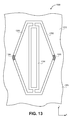
- FIG. 13 illustrates a plan view representing a MEMS structure having a diamond-shaped stress inverter member housing a resonator member, in accordance with an embodiment of the present invention.
- a MEMS structure 1300 is disposed above a substrate 1302 .
- MEMS structure 1300 includes a resonator member 1304 housed in an asymmetric stress inverter member 1306 coupled to substrate 1302 .
- Resonator member 1304 is suspended above substrate 1302 .
- a pair of driver and sensor electrodes, not shown, may be included on either side of resonator member 1304 .
- asymmetric stress inverter member 1306 is a diamond-shaped frame, as depicted in FIG. 13 .
- the diamond-shaped frame is directly coupled to substrate 1302 by a pair of anchor points 1308 .
- the diamond-shaped frame is oriented to have its major axis along the Y-axis and parallel with the longest dimension of resonator member 1304 , as is also depicted in FIG. 13 .
- the pair of anchor points 1308 is arranged orthogonally to the Y-axis and at the mid-point of the major axis, i.e. along the X-axis and parallel with the minor axis of the diamond-shaped frame.
- the CTE of asymmetric stress inverter member 1306 may be greater than the CTE of substrate 1302 (CTE 1 ).
- asymmetric stress inverter member 1306 is composed of silicon-germanium and substrate 1302 is composed of silicon.
- the TCf of resonator member 1304 is negative.
- asymmetric stress inverter member 1306 is provided to induce a tensile stress on resonator member 1304 in response to an increase in temperature.
- stress inverter member 1306 in response to a compressive (first) stress applied to stress inverter member 1306 due to CTE mismatch with substrate 1302 , stress inverter member 1306 deforms by expanding along the major axis (Y-axis) to provide a tensile (second) stress on resonator member 1304 .
- the tensile stress reduces the magnitude of the TCf of resonator member 1304 .
- the tensile stress essentially negates the TCf of resonator member 1304 .
- resonator member 1304 is composed of approximately the same material as asymmetric stress inverter member 1306 , e.g. both resonator member 1304 and asymmetric stress inverter member 1306 may be composed of silicon-germanium while substrate 1302 may be composed of silicon.
- resonator member 1304 is completely surrounded by stress inverter member 1306 , e.g., resonator member 1304 is completely surrounded by the diamond-shaped frame, as depicted in FIG. 13 .
- a diamond-shaped frame is utilized to partially decouple the effect of the substrate and stress inverter CTE mismatch.
- the specific dimensions of the diamond-shaped frame may be selected to fine-tune such partial decoupling.
- FIG. 14 is a correlation plot representing frequency variation as a function of temperature for a MEMS structure having a diamond-shaped stress inverter member housing a resonator member, in accordance with an embodiment of the present invention.
- the temperature response is provided for the frequency of a resonator member, housed in a diamond-shaped frame, as a function of the ratio of the major/minor axis (Y-over-X) parameters (axes shown in FIG. 13 ) for a variety of diamond-shaped geometries.
- the resonator member is a double-ended tuning-fork and the length of each beam of the resonator member is fixed at approximately 70 microns and the width of each beam is fixed at approximately 1.8 microns.
- the anti-symmetric mode (the 11 th mode) of the resonator member has a frequency of approximately 2.05 MHz.
- Correlation plot 1400 plots several correlations for major/minor (Y-over-X) diamond-shaped axes ratios, ranging from 2.80 to 3.00.
- the frequency of the resonator member with respect to changing temperature may be adjusted to a desired value.
- the frequency change of the resonator member over the temperature range of ⁇ 20-70 degrees Celsius can be approximately negated at a major/minor axes ratio (Y-over-X) of approximately 2.90. That is, in accordance with an embodiment of the present invention, the TCf of a resonator member is effectively zeroed-out by inducing a stress from a stress-inducer member on the resonator member in response to a changing temperature.
- an asymmetric frame applies a tensile stress to a resonator member in response to an increase in temperature
- an asymmetric frame is used to apply a compressive stress to a resonator member in response to a decrease in temperature.
- an asymmetric frame is used to apply a compressive stress to a resonator member in response to a increase in temperature.
- an asymmetric frame is used to apply a tensile stress to a resonator member in response to a decrease in temperature.
- an asymmetric frame is not limited to only an elliptical frame or a diamond-shaped frame. Rather, any frame having a major axis/minor axis pairing may be considered. Also, the longest dimension of a resonator housed in the asymmetric frame can be aligned with the major axis, the minor axis, or skewed between the major and the minor axis.
- an asymmetric frame may be anchored off-set from a mid-point of the frame or in a skewed fashion relative to the longest dimension of a resonator member housed therein or may further include decoupling members, such as decoupling rings or beams.
- the MEMS structure comprises a stress inverter member coupled with a substrate.
- a resonator member is housed in the stress inverter member and is suspended above the substrate.
- the MEMS stress inverter member is used to alter the TCf of the resonator member by inducing a stress on the resonator member in response to a change in temperature.
- the stress inverter member is coupled with the substrate via a pair of decoupling members.
- the pair of decoupling members is provided to reduce the magnitude of the stress induced on the resonator member.
- an array of n rows and m columns of stress inverter members is provided. Each stress inverter member houses a resonator member suspended above a substrate and is connected to a pair of decoupling members coupled with the substrate.
Abstract
Description
Claims (24)
Priority Applications (1)
| Application Number | Priority Date | Filing Date | Title |
|---|---|---|---|
| US12/204,713 US7956517B1 (en) | 2007-05-10 | 2008-09-04 | MEMS structure having a stress inverter temperature-compensated resonator member |
Applications Claiming Priority (2)
| Application Number | Priority Date | Filing Date | Title |
|---|---|---|---|
| US11/801,774 US7514853B1 (en) | 2007-05-10 | 2007-05-10 | MEMS structure having a stress inverter temperature-compensated resonating member |
| US12/204,713 US7956517B1 (en) | 2007-05-10 | 2008-09-04 | MEMS structure having a stress inverter temperature-compensated resonator member |
Related Parent Applications (1)
| Application Number | Title | Priority Date | Filing Date |
|---|---|---|---|
| US11/801,774 Continuation-In-Part US7514853B1 (en) | 2007-05-10 | 2007-05-10 | MEMS structure having a stress inverter temperature-compensated resonating member |
Publications (1)
| Publication Number | Publication Date |
|---|---|
| US7956517B1 true US7956517B1 (en) | 2011-06-07 |
Family
ID=44070872
Family Applications (1)
| Application Number | Title | Priority Date | Filing Date |
|---|---|---|---|
| US12/204,713 Active 2028-04-01 US7956517B1 (en) | 2007-05-10 | 2008-09-04 | MEMS structure having a stress inverter temperature-compensated resonator member |
Country Status (1)
| Country | Link |
|---|---|
| US (1) | US7956517B1 (en) |
Cited By (8)
| Publication number | Priority date | Publication date | Assignee | Title |
|---|---|---|---|---|
| US20100315179A1 (en) * | 2009-06-04 | 2010-12-16 | Sand9, Inc. | Methods and apparatus for temperature control of devices and mechanical resonating structures |
| US8476809B2 (en) | 2008-04-29 | 2013-07-02 | Sand 9, Inc. | Microelectromechanical systems (MEMS) resonators and related apparatus and methods |
| US20130214158A1 (en) * | 2011-08-17 | 2013-08-22 | Public Service Solutions, Inc. | Passive detectors for imaging systems |
| EP2713509A1 (en) * | 2012-09-27 | 2014-04-02 | Nxp B.V. | MEMS resonator with improved amplitude saturation |
| US8852984B1 (en) | 2011-03-30 | 2014-10-07 | Silicon Laboratories | Technique for forming a MEMS device |
| US8877536B1 (en) * | 2011-03-30 | 2014-11-04 | Silicon Laboratories Inc. | Technique for forming a MEMS device using island structures |
| US9048811B2 (en) | 2009-03-31 | 2015-06-02 | Sand 9, Inc. | Integration of piezoelectric materials with substrates |
| CN110902640A (en) * | 2019-12-11 | 2020-03-24 | 合肥工业大学 | High-sensitivity MEMS resonant temperature sensor chip |
Citations (28)
| Publication number | Priority date | Publication date | Assignee | Title |
|---|---|---|---|---|
| US5541469A (en) | 1993-04-14 | 1996-07-30 | Murata Manufacturing Co., Ltd. | Resonator utilizing width expansion mode |
| US5912528A (en) | 1995-04-03 | 1999-06-15 | Murata Manufacturing Co., Ltd. | Vibrating gyroscope |
| US20020069701A1 (en) * | 2000-08-24 | 2002-06-13 | Wan-Thai Hsu | Micromechanical resonator device |
| US20020154380A1 (en) | 2001-04-19 | 2002-10-24 | Daniel Gelbart | Method for controlling light beam using adaptive micro-lens |
| US20030006679A1 (en) | 2001-07-06 | 2003-01-09 | Hirofumi Kawashima | Width-extensional Mode piezoelectric crystal resonator |
| US6557419B1 (en) | 1996-12-31 | 2003-05-06 | Honeywell International Inc. | Zero TCF thin film resonator |
| US6686807B1 (en) | 1999-11-02 | 2004-02-03 | Eta Sa Fabriques D'ebauches | Time base comprising an integrated micromechanical ring resonator |
| US6708491B1 (en) | 2000-09-12 | 2004-03-23 | 3M Innovative Properties Company | Direct acting vertical thermal actuator |
| US20040207492A1 (en) * | 2002-12-17 | 2004-10-21 | Nguyen Clark T.-C. | Micromechanical resonator device and method of making a micromechanical device |
| US20050046504A1 (en) | 2003-08-12 | 2005-03-03 | Fujitsu Limited | Micro-oscillation element |
| US20050250236A1 (en) | 2004-05-04 | 2005-11-10 | The Regents Of The University Of California | Damascene process for use in fabricating semiconductor structures having micro/nano gaps |
| US6987432B2 (en) | 2003-04-16 | 2006-01-17 | Robert Bosch Gmbh | Temperature compensation for silicon MEMS resonator |
| US6996884B2 (en) | 2002-02-15 | 2006-02-14 | Seiko Instruments Inc. | Method for manufacturing piezo-electric vibrator |
| US20060033594A1 (en) | 2004-03-04 | 2006-02-16 | Markus Lutz | Temperature controlled MEMS resonator and method for controlling resonator frequency |
| US20060032306A1 (en) * | 2004-08-13 | 2006-02-16 | Commissariat A L'energie Atomique | Micro-gyrometer with frequency detection |
| US7023065B2 (en) | 2002-08-07 | 2006-04-04 | Georgia Tech Research Corporation | Capacitive resonators and methods of fabrication |
| US7211926B2 (en) | 2005-03-09 | 2007-05-01 | The Regents Of The University Of California | Temperature compensated oscillator including MEMS resonator for frequency control |
| US7300814B2 (en) | 2004-12-16 | 2007-11-27 | The Charles Stark Draper Laboratory, Inc. | Method for fabricating micro-mechanical devices |
| US20070296526A1 (en) * | 2005-05-19 | 2007-12-27 | Markus Lutz | Microelectromechanical resonator structure, and method of designing, operating and using same |
| US7350424B2 (en) | 2002-02-12 | 2008-04-01 | Nokia Corporation | Acceleration sensor |
| US20080105951A1 (en) | 2006-11-08 | 2008-05-08 | Seiko Epson Corporation | Electronic Device and Method for Manufacturing Thereof |
| US20080224241A1 (en) | 2007-03-15 | 2008-09-18 | Seiko Epson Corporation | Electronic device, resonator, oscillator and method for manufacturing electronic device |
| US7495199B2 (en) | 2006-02-10 | 2009-02-24 | Stmicroelectronics, Inc. | MEMS radiometer |
| US7514853B1 (en) * | 2007-05-10 | 2009-04-07 | Silicon Clocks, Inc. | MEMS structure having a stress inverter temperature-compensated resonating member |
| US20090160581A1 (en) | 2007-12-21 | 2009-06-25 | Paul Merritt Hagelin | Temperature Stable MEMS Resonator |
| US20090158566A1 (en) | 2007-12-21 | 2009-06-25 | Paul Merritt Hagelin | Temperature Stable MEMS Resonator |
| US7591201B1 (en) | 2007-03-09 | 2009-09-22 | Silicon Clocks, Inc. | MEMS structure having a compensated resonating member |
| US7639104B1 (en) | 2007-03-09 | 2009-12-29 | Silicon Clocks, Inc. | Method for temperature compensation in MEMS resonators with isolated regions of distinct material |
-
2008
- 2008-09-04 US US12/204,713 patent/US7956517B1/en active Active
Patent Citations (34)
| Publication number | Priority date | Publication date | Assignee | Title |
|---|---|---|---|---|
| US5541469A (en) | 1993-04-14 | 1996-07-30 | Murata Manufacturing Co., Ltd. | Resonator utilizing width expansion mode |
| US5912528A (en) | 1995-04-03 | 1999-06-15 | Murata Manufacturing Co., Ltd. | Vibrating gyroscope |
| US6557419B1 (en) | 1996-12-31 | 2003-05-06 | Honeywell International Inc. | Zero TCF thin film resonator |
| US6686807B1 (en) | 1999-11-02 | 2004-02-03 | Eta Sa Fabriques D'ebauches | Time base comprising an integrated micromechanical ring resonator |
| US20020069701A1 (en) * | 2000-08-24 | 2002-06-13 | Wan-Thai Hsu | Micromechanical resonator device |
| US6739190B2 (en) * | 2000-08-24 | 2004-05-25 | The Regents Of The University Of Michigan | Micromechanical resonator device |
| US6708491B1 (en) | 2000-09-12 | 2004-03-23 | 3M Innovative Properties Company | Direct acting vertical thermal actuator |
| US20020154380A1 (en) | 2001-04-19 | 2002-10-24 | Daniel Gelbart | Method for controlling light beam using adaptive micro-lens |
| US20030006679A1 (en) | 2001-07-06 | 2003-01-09 | Hirofumi Kawashima | Width-extensional Mode piezoelectric crystal resonator |
| US6717336B2 (en) | 2001-07-06 | 2004-04-06 | Piedek Technical Laboratory | Width-extensional mode piezoelectric crystal resonator |
| US7350424B2 (en) | 2002-02-12 | 2008-04-01 | Nokia Corporation | Acceleration sensor |
| US6996884B2 (en) | 2002-02-15 | 2006-02-14 | Seiko Instruments Inc. | Method for manufacturing piezo-electric vibrator |
| US7023065B2 (en) | 2002-08-07 | 2006-04-04 | Georgia Tech Research Corporation | Capacitive resonators and methods of fabrication |
| US20040207492A1 (en) * | 2002-12-17 | 2004-10-21 | Nguyen Clark T.-C. | Micromechanical resonator device and method of making a micromechanical device |
| US6987432B2 (en) | 2003-04-16 | 2006-01-17 | Robert Bosch Gmbh | Temperature compensation for silicon MEMS resonator |
| US7071793B2 (en) | 2003-04-16 | 2006-07-04 | Robert Bosch Gmbh | Temperature compensation for silicon MEMS resonator |
| US20060186971A1 (en) | 2003-04-16 | 2006-08-24 | Markus Lutz | Temperature compensation for silicon MEMS resonator |
| US7202761B2 (en) | 2003-04-16 | 2007-04-10 | Robert Bosch Gmbh | Temperature compensation for silicon MEMS resonator |
| US20050046504A1 (en) | 2003-08-12 | 2005-03-03 | Fujitsu Limited | Micro-oscillation element |
| US20060033594A1 (en) | 2004-03-04 | 2006-02-16 | Markus Lutz | Temperature controlled MEMS resonator and method for controlling resonator frequency |
| US20050250236A1 (en) | 2004-05-04 | 2005-11-10 | The Regents Of The University Of California | Damascene process for use in fabricating semiconductor structures having micro/nano gaps |
| US20060032306A1 (en) * | 2004-08-13 | 2006-02-16 | Commissariat A L'energie Atomique | Micro-gyrometer with frequency detection |
| US7300814B2 (en) | 2004-12-16 | 2007-11-27 | The Charles Stark Draper Laboratory, Inc. | Method for fabricating micro-mechanical devices |
| US7211926B2 (en) | 2005-03-09 | 2007-05-01 | The Regents Of The University Of California | Temperature compensated oscillator including MEMS resonator for frequency control |
| US20070296526A1 (en) * | 2005-05-19 | 2007-12-27 | Markus Lutz | Microelectromechanical resonator structure, and method of designing, operating and using same |
| US7495199B2 (en) | 2006-02-10 | 2009-02-24 | Stmicroelectronics, Inc. | MEMS radiometer |
| US20080105951A1 (en) | 2006-11-08 | 2008-05-08 | Seiko Epson Corporation | Electronic Device and Method for Manufacturing Thereof |
| US7591201B1 (en) | 2007-03-09 | 2009-09-22 | Silicon Clocks, Inc. | MEMS structure having a compensated resonating member |
| US7639104B1 (en) | 2007-03-09 | 2009-12-29 | Silicon Clocks, Inc. | Method for temperature compensation in MEMS resonators with isolated regions of distinct material |
| US20100093125A1 (en) | 2007-03-09 | 2010-04-15 | Quevy Emmanuel P | Method for temperature compensation in mems resonators with isolated regions of distinct material |
| US20080224241A1 (en) | 2007-03-15 | 2008-09-18 | Seiko Epson Corporation | Electronic device, resonator, oscillator and method for manufacturing electronic device |
| US7514853B1 (en) * | 2007-05-10 | 2009-04-07 | Silicon Clocks, Inc. | MEMS structure having a stress inverter temperature-compensated resonating member |
| US20090160581A1 (en) | 2007-12-21 | 2009-06-25 | Paul Merritt Hagelin | Temperature Stable MEMS Resonator |
| US20090158566A1 (en) | 2007-12-21 | 2009-06-25 | Paul Merritt Hagelin | Temperature Stable MEMS Resonator |
Non-Patent Citations (21)
| Title |
|---|
| Bernstein et al., "Mems Structure Having A Compensated Resonanting Member", U.S. Appl. No. 11/716,285, Amendment, May 27, 2009, 17 pgs. |
| Bernstein et al., "Mems Structure Having A Compensated Resonanting Member", U.S. Appl. No. 11/716,285, Notice Of Allowance, Jun. 22, 2009, 4 pgs. |
| Bernstein, "MEMS Structure Having A Stress-Inducer Temperature Compensated Resonator Member", U.S. Appl. No. 12/201,819, Amendment and Response to Office Action, Filed Feb. 11, 2011, 17 pgs. |
| Bernstein, "MEMS Structure Having a Stress-Inducer Temperature Compensated Resonator Member", U.S. Appl. No. 12/201,819, Notice of Allowance, Mailed Mar. 17, 2011, 11 pgs. |
| Bernstein, "MEMS Structure Having A Stress-Inducer Temperature Compensated Resonator Member", U.S. Appl. No. 12/201,819, Office Action, Filed Jan. 11, 2011, 9 pgs. |
| Bernstein, "MEMS Structure Having A Stress-Inducer Temperature. Compensated Resonator Member", U.S. Appl. No. 12/201,819, filed Aug. 29, 2008, 63 pgs. |
| Guckel, H. , et al., "Diagnostic Microstructures for the Measurement of Intrinsic Strain in Thin Films", J. Micromech. Microeng. 2, 1997, United Kingdom, (1997), 86-95. |
| Howe et al., "Mems Structure Having a Stress Inverter Temperature-Compensated Resonanting Member", U.S. Appl. No. 11/801,774, Amendment, Jul. 30, 2008, 16 pgs. |
| Howe et al., "Mems Structure Having A Stress Inverter Temperature-Compensated Resonanting Member", U.S. Appl. No. 11/801,774, Notice of Allowance, Nov. 26, 2008, 7 pgs. |
| Jianqiang, Han , et al., "Dependence of the resonance frequency of thermally excited microcantilever resonators on temperature", Elsevier, Sensors and Actuators, A101, (2002), 37-41. |
| Office Action from U.S. Appl. No. 11/716,115, mailed Oct. 6, 2008, 10 pgs. |
| Office Action from U.S. Appl. No. 11/716,285 mailed Feb. 27, 2009, 16 pgs. |
| Office Action from U.S. Appl. No. 11/801,774 mailed Apr. 30, 2008, 10 pgs. |
| Omura, Yoshiteru , et al., "New Resonant Accelerometer Based on Rigidity Change", International Conference on Solid-State Sensors and Actuators, Jun. 16-19, 1997, 855-858. |
| Quevy et al., "Method For Temperature Compensation In MEMS Resonators With Isolated Regions Of Distinct Material", U.S. Appl. No. 12/950,519, filed Nov. 19, 2010, 46 pgs. |
| Quevy et al., "Method For Temperature Compensation In MEMS Resonsators With Isolated Regions Of Distinct Material", U.S. Appl. No. 11/716,115, Notice Of Allowance, Apr. 7, 2009, 6 pgs. |
| Quevy et al., "Method For Temperature Compensation In MEMS Resonsators With Isolated Regions Of Distinct Material", U.S. Appl. No. 11/716,115, Notice Of Allowance, Aug. 10, 2009, 7 pgs. |
| Quevy et al., "Method For Temperature Compensation In MEMS Resonsators With Isolated Regions Of Distinct Material", U.S. Appl. No. 11/716,115, Request For Continued Examination Transmittal, Jul. 1, 2009, 1 pg. |
| Quevy et al., "Method For Temperature Compensation In MEMS Resonsators With Isolated Regions Of Distinct Material", U.S. Appl. No. 11/716,115, Response To Office Action, Jan. 6, 2009, 20 pgs. |
| Quevy, Emmanuel P., et al., "Redundant MEMS Resonators for Precise Reference Oscillators", IEEE Radio Frequency Integrated Circuits Symposium, Jun. 12-14, 2005, Long Beach, CA, (2005), 113-116. |
| Shen, F. , et al., "Thermal Effects on Coated Resonant Microcantilevers", Elsevier, Sensors and Actuators, A95, (2001), 17-23. |
Cited By (17)
| Publication number | Priority date | Publication date | Assignee | Title |
|---|---|---|---|---|
| US8476809B2 (en) | 2008-04-29 | 2013-07-02 | Sand 9, Inc. | Microelectromechanical systems (MEMS) resonators and related apparatus and methods |
| US8587183B2 (en) | 2008-04-29 | 2013-11-19 | Sand 9, Inc. | Microelectromechanical systems (MEMS) resonators and related apparatus and methods |
| US8698376B2 (en) | 2008-04-29 | 2014-04-15 | Sand 9, Inc. | Microelectromechanical systems (MEMS) resonators and related apparatus and methods |
| US9030080B2 (en) | 2008-04-29 | 2015-05-12 | Sand 9, Inc. | Microelectromechanical systems (MEMS) resonators and related apparatus and methods |
| US9048811B2 (en) | 2009-03-31 | 2015-06-02 | Sand 9, Inc. | Integration of piezoelectric materials with substrates |
| US20100315179A1 (en) * | 2009-06-04 | 2010-12-16 | Sand9, Inc. | Methods and apparatus for temperature control of devices and mechanical resonating structures |
| US8410868B2 (en) * | 2009-06-04 | 2013-04-02 | Sand 9, Inc. | Methods and apparatus for temperature control of devices and mechanical resonating structures |
| US9401693B2 (en) | 2009-06-04 | 2016-07-26 | Analog Devices, Inc. | Methods and apparatus for temperature control of devices and mechanical resonating structures |
| US8877536B1 (en) * | 2011-03-30 | 2014-11-04 | Silicon Laboratories Inc. | Technique for forming a MEMS device using island structures |
| US8852984B1 (en) | 2011-03-30 | 2014-10-07 | Silicon Laboratories | Technique for forming a MEMS device |
| US9260290B2 (en) | 2011-03-30 | 2016-02-16 | Silicon Laboratories Inc. | Technique for forming a MEMS device |
| US9012845B2 (en) * | 2011-08-17 | 2015-04-21 | Public Service Solutions, Inc. | Passive detectors for imaging systems |
| US20130214158A1 (en) * | 2011-08-17 | 2013-08-22 | Public Service Solutions, Inc. | Passive detectors for imaging systems |
| EP2713509A1 (en) * | 2012-09-27 | 2014-04-02 | Nxp B.V. | MEMS resonator with improved amplitude saturation |
| US9318997B2 (en) | 2012-09-27 | 2016-04-19 | Nxp, B.V. | Resonator |
| CN110902640A (en) * | 2019-12-11 | 2020-03-24 | 合肥工业大学 | High-sensitivity MEMS resonant temperature sensor chip |
| CN110902640B (en) * | 2019-12-11 | 2022-06-03 | 合肥工业大学 | High-sensitivity MEMS resonant temperature sensor chip |
Similar Documents
| Publication | Publication Date | Title |
|---|---|---|
| US7514853B1 (en) | MEMS structure having a stress inverter temperature-compensated resonating member | |
| US7956517B1 (en) | MEMS structure having a stress inverter temperature-compensated resonator member | |
| EP1925075B1 (en) | Breath-mode ring resonator structure, and method of designing, operating and using same | |
| EP3202035B1 (en) | Temperature compensated plate resonator | |
| JP6587681B2 (en) | Temperature compensated beam resonator | |
| US8669831B2 (en) | Method for temperature compensation in MEMS resonators with isolated regions of distinct material | |
| US8629739B2 (en) | Out-of plane MEMS resonator with static out-of-plane deflection | |
| US6987432B2 (en) | Temperature compensation for silicon MEMS resonator | |
| US7591201B1 (en) | MEMS structure having a compensated resonating member | |
| CN107408933B (en) | Temperature compensation composite resonator | |
| US20040113722A1 (en) | Mems resonator and method of making same | |
| US11277112B2 (en) | Micro-electro-mechanical device with reduced temperature sensitivity and manufacturing method thereof | |
| US7944124B1 (en) | MEMS structure having a stress-inducer temperature-compensated resonator member | |
| US8587390B2 (en) | MEMS vibrator, oscillator, and method for manufacturing MEMS vibrator | |
| CN116667807A (en) | Double-sided internal mode temperature compensation resonator | |
| EP2339748B1 (en) | Resonator | |
| US9695036B1 (en) | Temperature insensitive resonant elements and oscillators and methods of designing and manufacturing same | |
| CN105229923A (en) | The micro-electromechanical resonator improved | |
| WO2017168055A1 (en) | Stabile micromechanical devices |
Legal Events
| Date | Code | Title | Description |
|---|---|---|---|
| AS | Assignment |
Owner name: SILICON CLOCKS, INC., CALIFORNIA Free format text: ASSIGNMENT OF ASSIGNORS INTEREST;ASSIGNORS:MOTIEE, MEHRNAZ;HOWE, ROGER T.;QUEVY, EMMANUEL P.;AND OTHERS;SIGNING DATES FROM 20080829 TO 20080903;REEL/FRAME:021806/0894 |
|
| AS | Assignment |
Owner name: SILICON LABS SC, INC., CALIFORNIA Free format text: CHANGE OF NAME;ASSIGNOR:SILICON CLOCKS, INC.;REEL/FRAME:024369/0134 Effective date: 20100423 |
|
| AS | Assignment |
Owner name: SILICON LABORATORIES INC., TEXAS Free format text: ASSIGNMENT OF ASSIGNORS INTEREST;ASSIGNOR:SILICON LABS SC, INC.;REEL/FRAME:025366/0466 Effective date: 20101112 |
|
| FEPP | Fee payment procedure |
Free format text: PAYOR NUMBER ASSIGNED (ORIGINAL EVENT CODE: ASPN); ENTITY STATUS OF PATENT OWNER: LARGE ENTITY |
|
| STCF | Information on status: patent grant |
Free format text: PATENTED CASE |
|
| FPAY | Fee payment |
Year of fee payment: 4 |
|
| MAFP | Maintenance fee payment |
Free format text: PAYMENT OF MAINTENANCE FEE, 8TH YEAR, LARGE ENTITY (ORIGINAL EVENT CODE: M1552); ENTITY STATUS OF PATENT OWNER: LARGE ENTITY Year of fee payment: 8 |
|
| MAFP | Maintenance fee payment |
Free format text: PAYMENT OF MAINTENANCE FEE, 12TH YEAR, LARGE ENTITY (ORIGINAL EVENT CODE: M1553); ENTITY STATUS OF PATENT OWNER: LARGE ENTITY Year of fee payment: 12 |