US7952109B2 - Light-emitting crystal structures - Google Patents
Light-emitting crystal structures Download PDFInfo
- Publication number
- US7952109B2 US7952109B2 US11/456,428 US45642806A US7952109B2 US 7952109 B2 US7952109 B2 US 7952109B2 US 45642806 A US45642806 A US 45642806A US 7952109 B2 US7952109 B2 US 7952109B2
- Authority
- US
- United States
- Prior art keywords
- type
- group iii
- nitride
- quantum well
- layer
- Prior art date
- Legal status (The legal status is an assumption and is not a legal conclusion. Google has not performed a legal analysis and makes no representation as to the accuracy of the status listed.)
- Expired - Fee Related, expires
Links
- 239000013078 crystal Substances 0.000 title description 21
- 230000004888 barrier function Effects 0.000 claims description 130
- 239000000758 substrate Substances 0.000 claims description 31
- 229910002601 GaN Inorganic materials 0.000 claims description 12
- 229910000807 Ga alloy Inorganic materials 0.000 claims description 6
- JMASRVWKEDWRBT-UHFFFAOYSA-N Gallium nitride Chemical compound [Ga]#N JMASRVWKEDWRBT-UHFFFAOYSA-N 0.000 claims description 6
- 229910052782 aluminium Inorganic materials 0.000 claims description 6
- XAGFODPZIPBFFR-UHFFFAOYSA-N aluminium Chemical compound [Al] XAGFODPZIPBFFR-UHFFFAOYSA-N 0.000 claims description 6
- APFVFJFRJDLVQX-UHFFFAOYSA-N indium atom Chemical compound [In] APFVFJFRJDLVQX-UHFFFAOYSA-N 0.000 claims description 5
- 229910000846 In alloy Inorganic materials 0.000 claims description 2
- 229920002120 photoresistant polymer Polymers 0.000 description 13
- 238000000034 method Methods 0.000 description 12
- 239000000463 material Substances 0.000 description 9
- 239000000203 mixture Substances 0.000 description 8
- 230000005684 electric field Effects 0.000 description 7
- 238000001451 molecular beam epitaxy Methods 0.000 description 7
- 230000008569 process Effects 0.000 description 6
- 238000004519 manufacturing process Methods 0.000 description 5
- 229910052751 metal Inorganic materials 0.000 description 5
- 239000002184 metal Substances 0.000 description 5
- PXHVJJICTQNCMI-UHFFFAOYSA-N Nickel Chemical compound [Ni] PXHVJJICTQNCMI-UHFFFAOYSA-N 0.000 description 4
- RTAQQCXQSZGOHL-UHFFFAOYSA-N Titanium Chemical compound [Ti] RTAQQCXQSZGOHL-UHFFFAOYSA-N 0.000 description 4
- RNQKDQAVIXDKAG-UHFFFAOYSA-N aluminum gallium Chemical compound [Al].[Ga] RNQKDQAVIXDKAG-UHFFFAOYSA-N 0.000 description 4
- PCHJSUWPFVWCPO-UHFFFAOYSA-N gold Chemical compound [Au] PCHJSUWPFVWCPO-UHFFFAOYSA-N 0.000 description 4
- 229910052737 gold Inorganic materials 0.000 description 4
- 239000010931 gold Substances 0.000 description 4
- 229910052738 indium Inorganic materials 0.000 description 4
- 239000004065 semiconductor Substances 0.000 description 4
- 229910052719 titanium Inorganic materials 0.000 description 4
- 239000010936 titanium Substances 0.000 description 4
- 229910002704 AlGaN Inorganic materials 0.000 description 3
- 125000004429 atom Chemical group 0.000 description 3
- 238000005229 chemical vapour deposition Methods 0.000 description 3
- 238000000151 deposition Methods 0.000 description 3
- 239000002019 doping agent Substances 0.000 description 3
- 238000001039 wet etching Methods 0.000 description 3
- CSCPPACGZOOCGX-UHFFFAOYSA-N Acetone Chemical compound CC(C)=O CSCPPACGZOOCGX-UHFFFAOYSA-N 0.000 description 2
- GYHNNYVSQQEPJS-UHFFFAOYSA-N Gallium Chemical compound [Ga] GYHNNYVSQQEPJS-UHFFFAOYSA-N 0.000 description 2
- FYYHWMGAXLPEAU-UHFFFAOYSA-N Magnesium Chemical compound [Mg] FYYHWMGAXLPEAU-UHFFFAOYSA-N 0.000 description 2
- 229910045601 alloy Inorganic materials 0.000 description 2
- 239000000956 alloy Substances 0.000 description 2
- 230000015572 biosynthetic process Effects 0.000 description 2
- 239000011248 coating agent Substances 0.000 description 2
- 238000000576 coating method Methods 0.000 description 2
- PMHQVHHXPFUNSP-UHFFFAOYSA-M copper(1+);methylsulfanylmethane;bromide Chemical compound Br[Cu].CSC PMHQVHHXPFUNSP-UHFFFAOYSA-M 0.000 description 2
- 230000006872 improvement Effects 0.000 description 2
- 229910052749 magnesium Inorganic materials 0.000 description 2
- 239000011777 magnesium Substances 0.000 description 2
- 229910052759 nickel Inorganic materials 0.000 description 2
- 150000004767 nitrides Chemical class 0.000 description 2
- 229910052757 nitrogen Inorganic materials 0.000 description 2
- 125000004433 nitrogen atom Chemical group N* 0.000 description 2
- BASFCYQUMIYNBI-UHFFFAOYSA-N platinum Chemical compound [Pt] BASFCYQUMIYNBI-UHFFFAOYSA-N 0.000 description 2
- 230000010287 polarization Effects 0.000 description 2
- 229910052594 sapphire Inorganic materials 0.000 description 2
- 239000010980 sapphire Substances 0.000 description 2
- 229910052710 silicon Inorganic materials 0.000 description 2
- 239000010703 silicon Substances 0.000 description 2
- 229910052984 zinc sulfide Inorganic materials 0.000 description 2
- QAOWNCQODCNURD-UHFFFAOYSA-N Sulfuric acid Chemical compound OS(O)(=O)=O QAOWNCQODCNURD-UHFFFAOYSA-N 0.000 description 1
- XLOMVQKBTHCTTD-UHFFFAOYSA-N Zinc monoxide Chemical compound [Zn]=O XLOMVQKBTHCTTD-UHFFFAOYSA-N 0.000 description 1
- 230000004075 alteration Effects 0.000 description 1
- AUCDRFABNLOFRE-UHFFFAOYSA-N alumane;indium Chemical compound [AlH3].[In] AUCDRFABNLOFRE-UHFFFAOYSA-N 0.000 description 1
- NWAIGJYBQQYSPW-UHFFFAOYSA-N azanylidyneindigane Chemical compound [In]#N NWAIGJYBQQYSPW-UHFFFAOYSA-N 0.000 description 1
- 239000000969 carrier Substances 0.000 description 1
- 150000001875 compounds Chemical class 0.000 description 1
- 239000004020 conductor Substances 0.000 description 1
- 230000008878 coupling Effects 0.000 description 1
- 238000010168 coupling process Methods 0.000 description 1
- 238000005859 coupling reaction Methods 0.000 description 1
- 230000003247 decreasing effect Effects 0.000 description 1
- 238000000313 electron-beam-induced deposition Methods 0.000 description 1
- 238000005530 etching Methods 0.000 description 1
- YVPJCJLMRRTDMQ-UHFFFAOYSA-N ethyl diazoacetate Chemical compound CCOC(=O)C=[N+]=[N-] YVPJCJLMRRTDMQ-UHFFFAOYSA-N 0.000 description 1
- 229910052733 gallium Inorganic materials 0.000 description 1
- 239000007789 gas Substances 0.000 description 1
- 238000007654 immersion Methods 0.000 description 1
- PNHVEGMHOXTHMW-UHFFFAOYSA-N magnesium;zinc;oxygen(2-) Chemical compound [O-2].[O-2].[Mg+2].[Zn+2] PNHVEGMHOXTHMW-UHFFFAOYSA-N 0.000 description 1
- 229910001092 metal group alloy Inorganic materials 0.000 description 1
- 238000001465 metallisation Methods 0.000 description 1
- 230000003647 oxidation Effects 0.000 description 1
- 238000007254 oxidation reaction Methods 0.000 description 1
- 238000000059 patterning Methods 0.000 description 1
- 230000000737 periodic effect Effects 0.000 description 1
- 229910052697 platinum Inorganic materials 0.000 description 1
- 230000009467 reduction Effects 0.000 description 1
- 238000004528 spin coating Methods 0.000 description 1
- 230000002269 spontaneous effect Effects 0.000 description 1
- 238000006467 substitution reaction Methods 0.000 description 1
- 238000007736 thin film deposition technique Methods 0.000 description 1
- UMJICYDOGPFMOB-UHFFFAOYSA-N zinc;cadmium(2+);oxygen(2-) Chemical compound [O-2].[O-2].[Zn+2].[Cd+2] UMJICYDOGPFMOB-UHFFFAOYSA-N 0.000 description 1
Images


Classifications
-
- H—ELECTRICITY
- H01—ELECTRIC ELEMENTS
- H01L—SEMICONDUCTOR DEVICES NOT COVERED BY CLASS H10
- H01L33/00—Semiconductor devices with at least one potential-jump barrier or surface barrier specially adapted for light emission; Processes or apparatus specially adapted for the manufacture or treatment thereof or of parts thereof; Details thereof
- H01L33/02—Semiconductor devices with at least one potential-jump barrier or surface barrier specially adapted for light emission; Processes or apparatus specially adapted for the manufacture or treatment thereof or of parts thereof; Details thereof characterised by the semiconductor bodies
- H01L33/20—Semiconductor devices with at least one potential-jump barrier or surface barrier specially adapted for light emission; Processes or apparatus specially adapted for the manufacture or treatment thereof or of parts thereof; Details thereof characterised by the semiconductor bodies with a particular shape, e.g. curved or truncated substrate
- H01L33/24—Semiconductor devices with at least one potential-jump barrier or surface barrier specially adapted for light emission; Processes or apparatus specially adapted for the manufacture or treatment thereof or of parts thereof; Details thereof characterised by the semiconductor bodies with a particular shape, e.g. curved or truncated substrate of the light emitting region, e.g. non-planar junction
-
- H—ELECTRICITY
- H01—ELECTRIC ELEMENTS
- H01L—SEMICONDUCTOR DEVICES NOT COVERED BY CLASS H10
- H01L33/00—Semiconductor devices with at least one potential-jump barrier or surface barrier specially adapted for light emission; Processes or apparatus specially adapted for the manufacture or treatment thereof or of parts thereof; Details thereof
- H01L33/02—Semiconductor devices with at least one potential-jump barrier or surface barrier specially adapted for light emission; Processes or apparatus specially adapted for the manufacture or treatment thereof or of parts thereof; Details thereof characterised by the semiconductor bodies
- H01L33/20—Semiconductor devices with at least one potential-jump barrier or surface barrier specially adapted for light emission; Processes or apparatus specially adapted for the manufacture or treatment thereof or of parts thereof; Details thereof characterised by the semiconductor bodies with a particular shape, e.g. curved or truncated substrate
-
- H—ELECTRICITY
- H01—ELECTRIC ELEMENTS
- H01L—SEMICONDUCTOR DEVICES NOT COVERED BY CLASS H10
- H01L33/00—Semiconductor devices with at least one potential-jump barrier or surface barrier specially adapted for light emission; Processes or apparatus specially adapted for the manufacture or treatment thereof or of parts thereof; Details thereof
- H01L33/005—Processes
- H01L33/0062—Processes for devices with an active region comprising only III-V compounds
- H01L33/0075—Processes for devices with an active region comprising only III-V compounds comprising nitride compounds
-
- H—ELECTRICITY
- H01—ELECTRIC ELEMENTS
- H01L—SEMICONDUCTOR DEVICES NOT COVERED BY CLASS H10
- H01L33/00—Semiconductor devices with at least one potential-jump barrier or surface barrier specially adapted for light emission; Processes or apparatus specially adapted for the manufacture or treatment thereof or of parts thereof; Details thereof
- H01L33/02—Semiconductor devices with at least one potential-jump barrier or surface barrier specially adapted for light emission; Processes or apparatus specially adapted for the manufacture or treatment thereof or of parts thereof; Details thereof characterised by the semiconductor bodies
- H01L33/16—Semiconductor devices with at least one potential-jump barrier or surface barrier specially adapted for light emission; Processes or apparatus specially adapted for the manufacture or treatment thereof or of parts thereof; Details thereof characterised by the semiconductor bodies with a particular crystal structure or orientation, e.g. polycrystalline, amorphous or porous
- H01L33/18—Semiconductor devices with at least one potential-jump barrier or surface barrier specially adapted for light emission; Processes or apparatus specially adapted for the manufacture or treatment thereof or of parts thereof; Details thereof characterised by the semiconductor bodies with a particular crystal structure or orientation, e.g. polycrystalline, amorphous or porous within the light emitting region
-
- H—ELECTRICITY
- H01—ELECTRIC ELEMENTS
- H01L—SEMICONDUCTOR DEVICES NOT COVERED BY CLASS H10
- H01L33/00—Semiconductor devices with at least one potential-jump barrier or surface barrier specially adapted for light emission; Processes or apparatus specially adapted for the manufacture or treatment thereof or of parts thereof; Details thereof
- H01L33/02—Semiconductor devices with at least one potential-jump barrier or surface barrier specially adapted for light emission; Processes or apparatus specially adapted for the manufacture or treatment thereof or of parts thereof; Details thereof characterised by the semiconductor bodies
- H01L33/26—Materials of the light emitting region
- H01L33/30—Materials of the light emitting region containing only elements of group III and group V of the periodic system
- H01L33/32—Materials of the light emitting region containing only elements of group III and group V of the periodic system containing nitrogen
Definitions
- the present invention relates to an apparatus having a light emitting diode comprising a structure having a Group III-nitride, and a method of making the apparatus.
- One embodiment is an apparatus comprising a structure comprising a group III-nitride and a junction between n-type and p-type group III-nitride therein, the structure having a pyramidal shape or a wedge shape.
- Another embodiment is an apparatus comprising a light-emitting crystalline structure on a substrate.
- the structure has n-type and p-type barrier regions and a junction there between.
- the junction is located at one or more surfaces of the n-type and the p-type barrier regions that are inclined relative to a planar surface of the substrate.
- Another embodiment is a method manufacturing an apparatus.
- the method comprises forming a light-emitting crystalline structure that includes forming a first barrier region on a substrate, the first barrier region having one or more inclined surfaces relative to a planar surface of the substrate. Forming the structure also includes forming a second barrier region over the first barrier region, to form a junction at the inclined surfaces.
- the first barrier region comprises one of an n-type or p-type semiconductor crystal
- the second barrier region comprises the other of the n-type or p-type semiconductor crystal.
- FIG. 1 illustrates a perspective view of an example apparatus
- FIG. 2 illustrates a perspective view of an alternative example apparatus
- FIG. 3 illustrates a cross-sectional view of a portion of the example apparatus shown in FIG. 1 ;
- FIGS. 4-14 presents cross-sectional and plan views of an example apparatus at selected steps in an example method of manufacture.
- the present invention benefits from the recognition that both the intrinsic and extrinsic efficiency can be improved by forming light-emitting crystalline structures having an inclined surface.
- An improvement in internal efficiency can be achieved by altering the properties of the crystal material itself. Certain crystals, however, have no inversion symmetry along certain crystal axes, which causes the crystal to have an internal electric field. The internal electrical field detrimentally reduces the internal efficiency and can shift the wavelength of light emitted from such structures.
- Forming light emitting components of the structure on an inclined surface can render the structure a semi-polar or non-polar crystal, thereby decreasing or eliminating the internal electric field of the structure. Additionally, forming the structure on an inclined surface reduces the amount of light that gets internally reflected, thereby improving external efficiency.
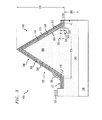
- FIG. 1 presents a perspective view of an example apparatus 100 , such as an LED or other illuminating apparatus comprising an LED.
- the apparatus 100 comprises a light-emitting crystalline structure 105 having an n-type barrier region 110 and a p-type barrier region 115 .
- junction 120 between the n-type and p-type barrier regions 110 , 115 . Portions of the interior p-type barrier region 115 and junction 120 are shown in a cut-away view in FIG. 1 .
- the junction 120 is located on an inclined surface 125 of one of the n-type or p-type barrier regions 110 , 115 .
- the incline of the surface 125 is relative to a planar surface 127 of a substrate 130 .
- the junction 120 comprises an active region that emits light when a voltage (V) is applied between the n-type and p-type regions 110 , 115 .
- V voltage
- the inclined surface 125 refers to a grown or wet etch-revealed surface of one of the n-type and p-type barrier regions 110 , 115 that deviates from the horizontal planar surface 127 of the substrate 130 that the structure 105 is located on.
- the horizontal plane 127 can correspond to a (0001) or a (000 1 ) plane of a substrate 130 (e.g., an insulating substrate such as sapphire) and the inclined surface 125 can correspond to one of the family of ⁇ 1 1 0 1 ⁇ planes.
- group III-nitride refers to a metal nitride or metal alloy nitride, where the metal comprises one or more atoms from Group III of the Periodic Table of Elements. Examples include aluminum nitride, gallium nitride, indium nitride, or combinations thereof.
- the n-type and p-type barrier regions 110 , 115 include dopants to form an n-type and p-type material. Examples of suitable n-type and p-type dopants include silicon and magnesium, respectively.
- the inclined surface 125 deviates from the horizontal planar surface 127 of the substrate 130 .
- the inclined surface 125 is configured to form an angle 135 that results in the reduction or cancellation of the internal electric field of the n-type or p-type barrier regions 110 , 115 .
- an angle 135 ranging from 55 to 65 degrees, and in some cases 55 to 60 degrees, causes the sum of piezoelectric polarization and spontaneous polarization in the junction 120 to cancel each other, resulting in a substantially zero electric field.
- the apparatus 100 can comprise a structure 105 comprising group III-nitrides and a junction 120 between n-type and p-type group III-nitrides therein 110 , 115 , the structure 105 having a pyramidal shape or a wedge shape.
- the structure 105 has a pyramidal shape, and more specifically a hexagonal pyramid.
- the inclined surface 125 corresponds to six facets 140 of the pyramid structure 105 located over the substrate 130 .
- the pyramid structure 105 can be formed using a wet etch process as discussed below.
- the structure 105 has a wedge shape.
- the inclined surface 125 corresponds to the two facets 210 of the wedge structure 105 located over the substrate 130 .
- the inclined surface 125 can correspond to one family of ⁇ 11 2 2 ⁇ planes.
- the wedge structure 105 can be formed by a chemical vapor deposition (CVD), such as described in Srinivasan et al., Applied Physics Letters 87:131911, 2005, which is incorporated by references in its entirety.
- CVD chemical vapor deposition
- the structures 105 it is desirable for the structures 105 to have a plurality of inclined surfaces 125 because this increases the external efficiency of the structure 105 .
- having a plurality of inclined surfaces 125 corresponding to the six facets 140 of the hexagonal pyramid structure 105 ( FIG. 1 ) is preferred over a structure 105 having a plurality of inclined surfaces 125 corresponding to the two facets 210 of the wedge structure 105 ( FIG. 2 ).
- the larger number of facets 140 of the pyramid structure 105 provides more surfaces for light to reflect off of at an angle that is below the critical angle of the crystal structure 105 , and therefore a greater number of escape routes from the structure 105 .
- FIG. 3 presents a cross-sectional view along view line 3 - 3 , which traverses through one of the facets 140 shown for the pyramidal-shaped structure 105 depicted in FIG. 1 .
- the cross-sectional view shown in FIG. 3 could also correspond to view line 3 - 3 , as depicted in FIG. 2 , which transverse through a plane perpendicular to the facets 210 of the wedge-shaped structure 105 .
- the junction 120 to include a quantum well 305 .
- the quantum well 305 comprise a group III-nitride.
- All three of the n-type region 110 , the p-type region 115 , and the quantum well 305 are pyramid-shaped when the structure 105 is pyramid-shaped. Alternately all three of the n-type region 110 , the p-type region 115 , and the quantum well 305 are wedge-shaped when the structure 105 is wedge-shaped. Having such configurations beneficially improves the internal light emission efficiency because it provides the inclined surface 125 needed to reduce the structure's 105 internal electric field. These configurations also advantageously improve the external light emission efficiency of the structure 105 . That is, there will be less internally reflected light from a quantum well 305 located on the inclined surface 125 compared to light from a quantum well of similar composition, but located on a planar surface.
- the composition of the group III-nitride of the quantum well 305 is different than the compositions of the group III-nitrides of n-type and p-type barrier regions 110 , 115 . It is important to select the compositions of the quantum well 305 and the n-type and p-type barrier regions 110 , 115 so as to configure the n-type and p-type barrier regions 110 , 115 to have a larger band gap than the quantum well 305 .
- Group III-nitrides having aluminum e.g. Al x Ga 1-x N
- a group III-nitride having indium e.g. In y Ga 1-y N
- the n-type and p-type barrier regions 110 , 115 comprises gallium nitride
- the quantum well 305 comprises an alloy of indium and gallium (e.g., indium gallium nitride).
- the n-type and p-type barrier regions 110 , 115 comprise an aluminum gallium alloy (e.g., aluminum gallium nitride) and the quantum well 305 comprises gallium nitride.
- n-type and p-type barrier regions 110 , 115 comprise an aluminum-rich aluminum gallium alloy (e.g., AlGaN having a ratio of Al:Ga:N of about 80:20:100) and the quantum well 305 comprises an aluminum-poor aluminum gallium alloy (e.g., AlGaN having a ratio of Al:Ga:N of about 60:40:100 AlGaN).
- the n-type and p-type barrier regions 110 , 115 comprise indium aluminum nitride or indium gallium aluminum nitride
- the quantum well 305 comprises indium gallium nitride.
- group III-nitrides alloys could be used.
- the quantum well 305 can have one or more quantum well layers 310 and one or more barrier layers 315 therein.
- Example quantum well layers 310 and barrier layers 315 are presented in U.S. Pat. No. 6,891,187 to Cho et al., which is incorporated by reference herein in its entirety.
- Each quantum well layer 310 is preferably interposed between barrier layers 315 .
- the quantum well layers 310 are separated from one another by barrier layers with a larger bandgap than the quantum well layers.
- each barrier layer 315 has a thickness 320 of about 10 to 50 Angstroms
- each quantum well layer 310 has a thickness 325 of about 5 to 50 Angstroms.
- the quantum well 305 comprises 1 to 8 quantum well layers 310 . Having multiple quantum well layers 310 beneficially increases the probability of carrier capture into the quantum well 305 . However, if there is too large a number of quantum well layers 310 , then carriers may not be distributed evenly through the different layers 310 .
- the quantum well region 310 and barrier layers 315 can comprise any of the combinations of the material described above for the quantum well 305 and the n-type and p-type regions 110 , 115 , respectively. It is preferable for the compositions of the quantum well region 310 and barrier layers 315 to be configured so that the quantum well region 310 has a narrow band gap and the barrier layers 315 has a wider band gap.
- the quantum well layer 310 can comprise one type of group III-nitride, while the barrier layers 315 can comprise another type of group III-nitride.
- the quantum well layer 310 can comprise InGaN, while the barrier layers 315 comprises GaN.
- the quantum well layer 310 comprises InGaN having a ratio of In:Ga:N ranging from about 15:85:100 to 20:80:100, and even more preferably, about 17:83:100.
- This composition is advantageous because the internal electric fields of the quantum well layers 310 are substantially reduced when located on an inclined surface 120 having an angle 135 of e.g., about 55 to 65° with respect to the substrate 130 . Such angles 135 are attained for the facets 140 , 210 of pyramidal ( FIG. 1 ) or wedge ( FIG. 2 ) shaped structures 105 that comprise, e.g., group III-nitrides.
- the quantum well 305 has a thickness 330 ranging from about 2.5 to 5 nanometers.
- the thickness 330 refers to the sum of the thicknesses of these layers 310 , 315 .
- Thin-film deposition techniques such as molecular beam epitaxy (MBE) can be used, e.g., to fabricate such a low thickness variation layers of quantum well 305 .
- MBE molecular beam epitaxy
- CVD can be used to produce quantum wells 305 whose thickness 330 varies by more than ⁇ 5%.
- the thickness 330 within any one structure 105 can range from about 2.5 to 5 nanometers.
- the p-type barrier region 115 is presented as an outer layer 340 of the structure 105
- the n-type barrier region 110 is shown as an interior region 345 of the structure 105 .
- the n-type barrier region 110 could be the outer layer 340 and the p-type barrier region 115 could be the interior region 345 .
- the junction 120 or optional quantum well 305 , is a middle layer 350 on the inclined surface 125 of the interior region 345 .
- the outer layer 340 comprising either one of an n-type or p-type group III-nitride that has a thickness 355 ranging from about 50 to 500 nanometers.
- the interior region 345 can comprise one or more pyramidal portion 360 located on a base portion 365 .
- the base 365 can be a substantially planar base that is part of the substrate 130 that the structure 105 is located on. For clarity only a single pyramid 360 is depicted in FIGS. 1 and 3 . However, in other embodiments the structure 105 comprises a plurality of pyramids 360 that are on a common base 365 . That is, the pyramids 360 are interconnected via the base 365 .
- Having the pyramids 360 interconnected via the base 365 facilitates the coupling of one of the n- or p-type barrier region 110 , 115 to ohmic contacts 150 , 155 that are in turn coupled to an electrical source 160 configured to apply a voltage (V) between these regions 110 , 115 .
- V voltage
- both the pyramid 360 and the base 365 are covered with the middle layer 350 of the quantum well 305 , and the outer layer 340 of the other of the n-type or p-type barrier regions 110 , 115 .
- the pyramid 360 has a height 370 and width 375 ranging from about 100 nm to 2 microns, and the base 365 has a thickness 380 of about 500 nm to 100 microns. It is desirable for the height 370 of the pyramid 360 to not exceed about 2 microns because taller structures can interfere with the formation of planar photoresist layers in subsequent processing steps.
- the pyramid 360 formed by a partial wet etch of the base 365 can be designed to remove material from a specific surface of crystal structures to reveal the pyramid 360 . Examples of such wet-etch processes are presented in U.S. Pat. No. 6,986,693 to Chowdhury et al., which is incorporated by reference herein in its totality.
- N-polar nitrogen-polar
- M-polar metal-polar
- N-polar surface refers to a face of a Group III-nitride Wurtzite structure having a straight bond (in a tetragonal bonding configuration) from a Nitrogen atom to a Group III metal atom.
- An M-polar surface refers to a face having the straight bond from a Group III metal atom to the Nitrogen atom.
- the base wet etch etches the ⁇ 1 1 0 1 ⁇ planes of a Group III-nitride crystal (e.g., GaN) to produce a hexagonal-shaped pyramidal structure 105 ( FIG. 1 ).
- the hexagonal pyramidal structure 105 has six facets 140 of the ⁇ 1 1 0 1 ⁇ family.
- the hexagonal-shaped pyramidal shaped structure 105 has a base-to-facet angle 135 of about 58.4 degrees.
- the p-ohmic contact 150 touches the p-type barrier region 115 and the n-ohmic contact 155 touches the n-type barrier region 110 .
- the ohmic contacts 150 , 155 comprise one or more layers of conductive material such as titanium, aluminum, nickel, platinum, gold or alloys thereof.
- the electrical source 160 is configured to apply a voltage (e.g., V of about 0.5 to 10 Volts, in some embodiments) to the ohmic contacts 150 , 155 so as to cause the structure 105 to emitting light.
- FIGS. 4-20 show cross-sectional views of selected steps in an example method of manufacturing an apparatus 400 . Any of the embodiments of the example apparatuses depicted in FIGS. 1 and 3 could be manufactured by the method.
- FIGS. 4-8 show selected steps in forming a light-emitting crystalline structure 405 of the apparatus 400 .
- Forming the structure includes forming a first barrier region on a substrate, the first barrier region having one or more inclined surfaces relative to a planar surface of the substrate.
- FIG. 4-7 illustrate selected steps in forming the first barrier region.
- FIG. 4 shows the apparatus 400 after forming a barrier region seed layer 407 on a substrate 410 .
- Sapphire is a preferred substrate 410 because it facilitates formation of a subsequently grown N-polar barrier region on the substrate 410 .
- Forming the barrier region seed layer 407 can comprise growing, via MBE, an AlN seed layer 415 (thickness 417 of about 20 nm) on the substrate 410 and a group III-nitride (e.g., GaN) seed layer 420 (thickness 422 of about 50 nm) on the AlN seed layer 415 .
- the AlN seed layer 415 is preferred because it facilitates the growth of a subsequently grown M-polar barrier region on the substrate 410 .
- FIG. 4 also illustrates the apparatus 400 after depositing a photoresist layer 425 , e.g., by spin coating, and patterning the photoresist layer 425 to form one or more openings 430 .
- the openings 430 define locations on the substrate 410 where light-emitting crystalline structures 405 are formed.
- FIG. 5 shows the apparatus 400 after removing portions of the barrier region seed layer 407 that are exposed in the opening 430 , and then removing the photoresist layer 425 ( FIG. 4 ).
- a plasma etch comprising Cl and Ar can be used to remove the exposed portions of barrier region seed layer 407 to extend the opening 430 down to the substrate 410 .
- the gas composition can comprise 30 sccm Cl and 10 sccm Ar.
- the photoresist 425 is then removed by a conventional process, such as immersion in acetone, followed by 10:1 (by volume) H 2 SO 4 :H 2 O 2 .
- FIG. 6 shows the apparatus after forming a layer of first barrier region 605 on the substrate 410 and on the group III-nitride seed layer 420 .
- MBE can be used to grow a layer of first barrier region 605 that comprises a group III-nitride and has a thickness 607 ranging from about 1 to 5 micron.
- the group III-nitride of the first barrier region 605 can be substantially similar in composition to the group III-nitride seed layer 420 of the seed layer 407 .
- the first barrier region 605 and group III-nitride seed layer 420 can both comprise GaN.
- the first barrier region 605 comprises one of an n-type or p-type semiconductor crystal to thereby form an n-type barrier region or p-type barrier region.
- suitable n-type or p-type dopants such as silicon or magnesium, respectively, can be included during the MBE growth of the first barrier region 605 .
- Preferred embodiments of the layer of first barrier region 605 comprise a grown M-polar surface 610 and a grown N-polar surface 615 . That is, the layer of first barrier region 605 grown on the barrier region seed layer 407 has the M-polar surface 610 , while the layer of first barrier region 605 grown on the substrate 410 that is exposed in the opening 430 has the N-polar surface 615 . It is advantageous for the first barrier region 605 to have both the M-polar and N-polar surfaces 610 , 615 because this allows one to predefine the location on the substrate 410 where the inclined surface of the first barrier region 605 will be formed.
- an inclined surface 705 can be formed by wet etching the N-polar surfaces 615 , e.g., with a base as discussed above and in U.S. Pat. No. 6,986,693.
- the M-polar surface 610 of the first barrier region 605 is comparatively unaffected by the wet etch.
- the first barrier region 605 comprises Group III-nitrides (e.g., GaN)
- wet etching the N-polar surfaces 615 causes rapid etching of the family of ⁇ 1 1 0 1 ⁇ planes to form one or more hexagonal pyramid 710 .
- the inclined surfaces 705 comprise facets 715 of the pyramid 710 .
- the inclined surface 705 can form an angle 720 ranging from about 55 to 65° with respect to a horizontal planar surface 725 of the substrate 410 .
- the wet etching can form a plurality of interconnected pyramids 710 on a base portion 730 of the first barrier region 605 .
- the pyramids 710 and the base portion 730 both comprise a same material of the first barrier region 605 .
- FIG. 8 shows the apparatus 100 after forming a second barrier region 805 over the first barrier region 605 , thereby forming a junction 810 at the inclined surfaces 705 .
- the second barrier region 805 comprises the other of the n-type or p-type semiconductor crystal that the first barrier region 605 does not comprise.
- Preferred embodiments of the second barrier region 805 comprise a group III-nitride.
- MBE can be used to grow a layer of the second barrier region 805 that comprises a group III-nitride having a thickness 815 ranging from about 50 to 500 nanometers. MBE is preferred because it can form the second barrier region 805 with a minimum variation in the thickness 815 .
- the second barrier region 805 is deposited over, and in some cases on, the plurality of interconnected pyramids 710 on a base portion 730 .
- a quantum well 820 can be formed on the first barrier region 605 before forming the second barrier region 805 .
- the junction 810 comprises the quantum well 820 .
- the quantum well 820 comprising a group III-nitride can be formed, e.g., via MBE on the plurality of interconnected pyramids 710 on a base portion 730 , and then the second barrier region 805 is formed on the quantum well 820 .
- FIGS. 9-13 show selected steps in forming contacts to the first and second barrier regions 605 , 805 .
- FIG. 9 shows the apparatus 100 after filling the opening 430 , with second photoresist 905 .
- the photoresist 905 thereby covers portions of the first barrier region 605 , the second barrier region 805 and optional quantum well 820 that are located inside the opening 430 .
- FIG. 10 illustrates the apparatus 100 after exposing the M-polar surface 610 of the first barrier region 605 .
- a plasma etch comprising Ar and Cl can be used to remove the portions of the second barrier region 805 and the optional quantum well 820 , that are outside of the opening 430 and not covered with the photoresist 905 .
- the photoresist 905 protects the first barrier region 605 , the second barrier region 805 and optional quantum well 820 in the opening 430 from being etched. Thereafter, the photoresist 905 is removed.
- FIG. 11 depicts the apparatus 100 after depositing a first ohmic contact 1105 on the M-polar surface 610 of the first barrier region 605 .
- the first ohmic contact 1105 can be formed by a conventional metal lift-off process.
- a third photoresist 1110 can be deposited and patterned to form an opening 1115 to the barrier region 605 and located around the light-emitting crystal structure 405 .
- the material of the first contact 1105 e.g., aluminum, titanium, gold
- first contact 1105 comprises four consecutively deposited layers of titanium, aluminum, titanium, and gold on the first barrier region 605 configured as an n-type barrier region.
- FIG. 12 shows the apparatus 100 after depositing a second ohmic contact 1205 on the second barrier region 805 .
- a fourth photoresist 1210 can be deposited and patterned to form an opening 1215 to the second barrier region 805 and located within the light-emitting crystal structure 405 .
- the second barrier region 805 is located over or on the N-polar surface 615 of the first barrier region 605 and the second contact 1205 is over or on the second barrier region 805 .
- the second ohmic contact 1205 comprises a different material than the first contact 1105 .
- second contact 1205 comprises two consecutively deposited layers of nickel and gold on the second barrier region 805 configured as a p-type barrier region.
- FIG. 13 depicts the apparatus 100 after lifting-off the photoresist layer 1210 ( FIG. 12 ).
- FIG. 14 shows a plan view of the apparatus 100 such as depicted in FIG. 13 .
- the first contact 1105 need not cover the entire M-polar surface 610 . This follows because the portion of the first barrier region 605 having the M-polar surface 610 is in electrical contact with portion of the first barrier region 605 having the N-polar surface 615 . E.g., the base 730 below the pyramids 710 touches the first barrier region 605 that is under the M-polar surface 610 . Therefore, the first contact 1105 is also in electrical contact with the inclined surfaces 705 and the junction 810 of the structure 405 .
- the second contact 1205 does not need to cover the entire second barrier region 805 formed on each inclined surface 705 of the structure.
- the second barrier region 805 forms a uniform coating over interconnected pyramids 710 and the base 730 of the first barrier region 605
- a second contact 1205 touching any portion of the second barrier region 805 is also in electrical contact with the inclined surfaces 705 and the junction 810 of the structure 405 .
- Having the structure 405 comprise a uniform coating of second barrier region 805 over a plurality interconnected pyramids 710 advantageously allows one more flexibility as to the placement of the second contact 1205 . This avoids the need to align the second contact 1205 with a specific location on each pyramid 710 , which can problematic because the exact location of where a pyramid 710 will form by the wet etch process can be unpredictable.
Abstract
Description
Claims (20)
Priority Applications (7)
| Application Number | Priority Date | Filing Date | Title |
|---|---|---|---|
| US11/456,428 US7952109B2 (en) | 2006-07-10 | 2006-07-10 | Light-emitting crystal structures |
| JP2009519426A JP2009543372A (en) | 2006-07-10 | 2007-03-06 | Luminescent crystal structure |
| PCT/US2007/005597 WO2008008097A1 (en) | 2006-07-10 | 2007-03-06 | Light-emitting crystal structures |
| EP07752311A EP2041803A1 (en) | 2006-07-10 | 2007-03-06 | Light-emitting crystal structures |
| CNA2007800260365A CN101490859A (en) | 2006-07-10 | 2007-03-06 | Light-emitting crystal structures |
| KR1020097000388A KR20090018721A (en) | 2006-07-10 | 2007-03-06 | Light-emitting crystal structures |
| US12/852,877 US20100304516A1 (en) | 2006-07-10 | 2010-08-09 | Light-emitting crystal structures |
Applications Claiming Priority (1)
| Application Number | Priority Date | Filing Date | Title |
|---|---|---|---|
| US11/456,428 US7952109B2 (en) | 2006-07-10 | 2006-07-10 | Light-emitting crystal structures |
Related Child Applications (1)
| Application Number | Title | Priority Date | Filing Date |
|---|---|---|---|
| US12/852,877 Division US20100304516A1 (en) | 2006-07-10 | 2010-08-09 | Light-emitting crystal structures |
Publications (2)
| Publication Number | Publication Date |
|---|---|
| US20080006831A1 US20080006831A1 (en) | 2008-01-10 |
| US7952109B2 true US7952109B2 (en) | 2011-05-31 |
Family
ID=38328558
Family Applications (2)
| Application Number | Title | Priority Date | Filing Date |
|---|---|---|---|
| US11/456,428 Expired - Fee Related US7952109B2 (en) | 2006-07-10 | 2006-07-10 | Light-emitting crystal structures |
| US12/852,877 Abandoned US20100304516A1 (en) | 2006-07-10 | 2010-08-09 | Light-emitting crystal structures |
Family Applications After (1)
| Application Number | Title | Priority Date | Filing Date |
|---|---|---|---|
| US12/852,877 Abandoned US20100304516A1 (en) | 2006-07-10 | 2010-08-09 | Light-emitting crystal structures |
Country Status (6)
| Country | Link |
|---|---|
| US (2) | US7952109B2 (en) |
| EP (1) | EP2041803A1 (en) |
| JP (1) | JP2009543372A (en) |
| KR (1) | KR20090018721A (en) |
| CN (1) | CN101490859A (en) |
| WO (1) | WO2008008097A1 (en) |
Cited By (9)
| Publication number | Priority date | Publication date | Assignee | Title |
|---|---|---|---|---|
| US20100295014A1 (en) * | 2006-08-16 | 2010-11-25 | Xuejun Kang | Improvements in external light efficiency of light emitting diodes |
| US20110186810A1 (en) * | 2010-02-01 | 2011-08-04 | Hermes-Epitek Corp. | Optoelectronic component with three-dimension quantum well structure and method for producing the same |
| US8809832B1 (en) * | 2011-04-14 | 2014-08-19 | Opto Tech Corporation | Method of selective photo-enhanced wet oxidation for nitride layer regrowth on substrates and associated structure |
| US9142722B2 (en) | 2013-03-15 | 2015-09-22 | Samsung Electronics Co., Ltd. | Semiconductor light emitting device and illumination apparatus including the same |
| US9202967B2 (en) | 2011-03-03 | 2015-12-01 | Osram Opto Semiconductors Gmbh | Method for producing a thin-film semiconductor body and thin-film semiconductor body |
| US20160056326A1 (en) * | 2013-04-10 | 2016-02-25 | Osram Opto Semiconductors Gmbh | Optoelectronic Semiconductor Chip and Method for the Production Thereof |
| US9337389B2 (en) * | 2012-06-26 | 2016-05-10 | Polar Light Technologies Ab | Group-III nitride structure |
| US9412900B2 (en) * | 2014-08-21 | 2016-08-09 | AICT (Advanced Institutes of Convergence Technology) | Green-light emitting device including quaternary quantum well on vicinal c-plane |
| USRE47767E1 (en) * | 2003-03-26 | 2019-12-17 | Nokia Of America Corporation | Group III-nitride layers with patterned surfaces |
Families Citing this family (73)
| Publication number | Priority date | Publication date | Assignee | Title |
|---|---|---|---|---|
| US7842527B2 (en) | 2006-12-11 | 2010-11-30 | The Regents Of The University Of California | Metalorganic chemical vapor deposition (MOCVD) growth of high performance non-polar III-nitride optical devices |
| US7982205B2 (en) * | 2006-01-12 | 2011-07-19 | National Institute Of Advanced Industrial Science And Technology | III-V group compound semiconductor light-emitting diode |
| KR100755598B1 (en) * | 2006-06-30 | 2007-09-06 | 삼성전기주식회사 | Nitride semiconductor light emitting diode array |
| TWI492411B (en) * | 2006-12-11 | 2015-07-11 | Univ California | Non-polar and semi-polar light emitting devices |
| JP5003527B2 (en) * | 2008-02-22 | 2012-08-15 | 住友電気工業株式会社 | Group III nitride light emitting device and method for fabricating group III nitride semiconductor light emitting device |
| US8097081B2 (en) | 2008-06-05 | 2012-01-17 | Soraa, Inc. | High pressure apparatus and method for nitride crystal growth |
| US20090301388A1 (en) * | 2008-06-05 | 2009-12-10 | Soraa Inc. | Capsule for high pressure processing and method of use for supercritical fluids |
| US8871024B2 (en) * | 2008-06-05 | 2014-10-28 | Soraa, Inc. | High pressure apparatus and method for nitride crystal growth |
| US9157167B1 (en) | 2008-06-05 | 2015-10-13 | Soraa, Inc. | High pressure apparatus and method for nitride crystal growth |
| US20090320745A1 (en) * | 2008-06-25 | 2009-12-31 | Soraa, Inc. | Heater device and method for high pressure processing of crystalline materials |
| US9404197B2 (en) | 2008-07-07 | 2016-08-02 | Soraa, Inc. | Large area, low-defect gallium-containing nitride crystals, method of making, and method of use |
| US8124996B2 (en) | 2008-08-04 | 2012-02-28 | Soraa, Inc. | White light devices using non-polar or semipolar gallium containing materials and phosphors |
| US8979999B2 (en) * | 2008-08-07 | 2015-03-17 | Soraa, Inc. | Process for large-scale ammonothermal manufacturing of gallium nitride boules |
| US10036099B2 (en) | 2008-08-07 | 2018-07-31 | Slt Technologies, Inc. | Process for large-scale ammonothermal manufacturing of gallium nitride boules |
| US8323405B2 (en) * | 2008-08-07 | 2012-12-04 | Soraa, Inc. | Process and apparatus for growing a crystalline gallium-containing nitride using an azide mineralizer |
| US8430958B2 (en) * | 2008-08-07 | 2013-04-30 | Soraa, Inc. | Apparatus and method for seed crystal utilization in large-scale manufacturing of gallium nitride |
| US8021481B2 (en) | 2008-08-07 | 2011-09-20 | Soraa, Inc. | Process and apparatus for large-scale manufacturing of bulk monocrystalline gallium-containing nitride |
| US7976630B2 (en) | 2008-09-11 | 2011-07-12 | Soraa, Inc. | Large-area seed for ammonothermal growth of bulk gallium nitride and method of manufacture |
| US8354679B1 (en) * | 2008-10-02 | 2013-01-15 | Soraa, Inc. | Microcavity light emitting diode method of manufacture |
| US20100295088A1 (en) * | 2008-10-02 | 2010-11-25 | Soraa, Inc. | Textured-surface light emitting diode and method of manufacture |
| US8455894B1 (en) | 2008-10-17 | 2013-06-04 | Soraa, Inc. | Photonic-crystal light emitting diode and method of manufacture |
| US8878230B2 (en) * | 2010-03-11 | 2014-11-04 | Soraa, Inc. | Semi-insulating group III metal nitride and method of manufacture |
| US9543392B1 (en) | 2008-12-12 | 2017-01-10 | Soraa, Inc. | Transparent group III metal nitride and method of manufacture |
| USRE47114E1 (en) | 2008-12-12 | 2018-11-06 | Slt Technologies, Inc. | Polycrystalline group III metal nitride with getter and method of making |
| US8987156B2 (en) | 2008-12-12 | 2015-03-24 | Soraa, Inc. | Polycrystalline group III metal nitride with getter and method of making |
| US20100147210A1 (en) * | 2008-12-12 | 2010-06-17 | Soraa, Inc. | high pressure apparatus and method for nitride crystal growth |
| US8461071B2 (en) * | 2008-12-12 | 2013-06-11 | Soraa, Inc. | Polycrystalline group III metal nitride with getter and method of making |
| US9589792B2 (en) | 2012-11-26 | 2017-03-07 | Soraa, Inc. | High quality group-III metal nitride crystals, methods of making, and methods of use |
| US20110100291A1 (en) * | 2009-01-29 | 2011-05-05 | Soraa, Inc. | Plant and method for large-scale ammonothermal manufacturing of gallium nitride boules |
| TW201032350A (en) * | 2009-02-20 | 2010-09-01 | Univ Nat Central | A manufacturing method of LED |
| US8299473B1 (en) | 2009-04-07 | 2012-10-30 | Soraa, Inc. | Polarized white light devices using non-polar or semipolar gallium containing materials and transparent phosphors |
| US10108079B2 (en) | 2009-05-29 | 2018-10-23 | Soraa Laser Diode, Inc. | Laser light source for a vehicle |
| US9250044B1 (en) | 2009-05-29 | 2016-02-02 | Soraa Laser Diode, Inc. | Gallium and nitrogen containing laser diode dazzling devices and methods of use |
| US8427590B2 (en) | 2009-05-29 | 2013-04-23 | Soraa, Inc. | Laser based display method and system |
| US9829780B2 (en) | 2009-05-29 | 2017-11-28 | Soraa Laser Diode, Inc. | Laser light source for a vehicle |
| US8509275B1 (en) | 2009-05-29 | 2013-08-13 | Soraa, Inc. | Gallium nitride based laser dazzling device and method |
| US9800017B1 (en) | 2009-05-29 | 2017-10-24 | Soraa Laser Diode, Inc. | Laser device and method for a vehicle |
| US8750342B1 (en) | 2011-09-09 | 2014-06-10 | Soraa Laser Diode, Inc. | Laser diodes with scribe structures |
| US8435347B2 (en) | 2009-09-29 | 2013-05-07 | Soraa, Inc. | High pressure apparatus with stackable rings |
| US9175418B2 (en) | 2009-10-09 | 2015-11-03 | Soraa, Inc. | Method for synthesis of high quality large area bulk gallium based crystals |
| US9564320B2 (en) | 2010-06-18 | 2017-02-07 | Soraa, Inc. | Large area nitride crystal and method for making it |
| US8729559B2 (en) | 2010-10-13 | 2014-05-20 | Soraa, Inc. | Method of making bulk InGaN substrates and devices thereon |
| US8786053B2 (en) | 2011-01-24 | 2014-07-22 | Soraa, Inc. | Gallium-nitride-on-handle substrate materials and devices and method of manufacture |
| KR101964890B1 (en) * | 2011-07-12 | 2019-04-03 | 삼성전자주식회사 | Nano-structured light emitting device |
| US8492185B1 (en) | 2011-07-14 | 2013-07-23 | Soraa, Inc. | Large area nonpolar or semipolar gallium and nitrogen containing substrate and resulting devices |
| US9694158B2 (en) | 2011-10-21 | 2017-07-04 | Ahmad Mohamad Slim | Torque for incrementally advancing a catheter during right heart catheterization |
| US10029955B1 (en) | 2011-10-24 | 2018-07-24 | Slt Technologies, Inc. | Capsule for high pressure, high temperature processing of materials and methods of use |
| US8482104B2 (en) | 2012-01-09 | 2013-07-09 | Soraa, Inc. | Method for growth of indium-containing nitride films |
| US10145026B2 (en) | 2012-06-04 | 2018-12-04 | Slt Technologies, Inc. | Process for large-scale ammonothermal manufacturing of semipolar gallium nitride boules |
| US9275912B1 (en) | 2012-08-30 | 2016-03-01 | Soraa, Inc. | Method for quantification of extended defects in gallium-containing nitride crystals |
| CN102867896B (en) * | 2012-09-26 | 2015-10-14 | 湘能华磊光电股份有限公司 | LED epitaxial structure and preparation method thereof |
| US9299555B1 (en) | 2012-09-28 | 2016-03-29 | Soraa, Inc. | Ultrapure mineralizers and methods for nitride crystal growth |
| RU2015132897A (en) * | 2013-01-08 | 2017-02-14 | Конинклейке Филипс Н.В. | SPECIAL FORM LIGHT-RADIATING DIODE DEVICE FOR IMPROVED EFFICIENCY OF EMISSION OF LIGHT |
| US9650723B1 (en) | 2013-04-11 | 2017-05-16 | Soraa, Inc. | Large area seed crystal for ammonothermal crystal growth and method of making |
| CN105449053B (en) * | 2014-09-19 | 2018-04-03 | 展晶科技(深圳)有限公司 | LED crystal particle and its manufacture method |
| CN104465929B (en) * | 2014-11-07 | 2017-09-12 | 中山大学 | The III-nitride micro-nano luminescent device and preparation method of embedded active layer |
| FR3032064B1 (en) * | 2015-01-22 | 2018-03-09 | Aledia | OPTOELECTRONIC DEVICE AND METHOD FOR MANUFACTURING THE SAME |
| US9787963B2 (en) | 2015-10-08 | 2017-10-10 | Soraa Laser Diode, Inc. | Laser lighting having selective resolution |
| ES2808920T3 (en) | 2015-11-06 | 2021-03-02 | Hoffmann La Roche | Indolin-2-one derivatives |
| DE102016103346A1 (en) * | 2016-02-25 | 2017-08-31 | Osram Opto Semiconductors Gmbh | Method for producing a radiation-emitting semiconductor chip and radiation-emitting semiconductor chip |
| WO2018062252A1 (en) * | 2016-09-29 | 2018-04-05 | 日亜化学工業株式会社 | Light emitting element |
| US10193018B2 (en) * | 2016-12-29 | 2019-01-29 | Intel Corporation | Compact low power head-mounted display with light emitting diodes that exhibit a desired beam angle |
| US10174438B2 (en) | 2017-03-30 | 2019-01-08 | Slt Technologies, Inc. | Apparatus for high pressure reaction |
| DE102017120037A1 (en) * | 2017-08-31 | 2019-02-28 | Osram Opto Semiconductors Gmbh | Method for producing a plurality of radiation-emitting semiconductor chips, radiation-emitting semiconductor chip and radiation-emitting semiconductor chip array |
| US10771155B2 (en) | 2017-09-28 | 2020-09-08 | Soraa Laser Diode, Inc. | Intelligent visible light with a gallium and nitrogen containing laser source |
| US10222474B1 (en) | 2017-12-13 | 2019-03-05 | Soraa Laser Diode, Inc. | Lidar systems including a gallium and nitrogen containing laser light source |
| US10551728B1 (en) | 2018-04-10 | 2020-02-04 | Soraa Laser Diode, Inc. | Structured phosphors for dynamic lighting |
| US11239637B2 (en) | 2018-12-21 | 2022-02-01 | Kyocera Sld Laser, Inc. | Fiber delivered laser induced white light system |
| US11421843B2 (en) | 2018-12-21 | 2022-08-23 | Kyocera Sld Laser, Inc. | Fiber-delivered laser-induced dynamic light system |
| US11466384B2 (en) | 2019-01-08 | 2022-10-11 | Slt Technologies, Inc. | Method of forming a high quality group-III metal nitride boule or wafer using a patterned substrate |
| US11884202B2 (en) | 2019-01-18 | 2024-01-30 | Kyocera Sld Laser, Inc. | Laser-based fiber-coupled white light system |
| US11705322B2 (en) | 2020-02-11 | 2023-07-18 | Slt Technologies, Inc. | Group III nitride substrate, method of making, and method of use |
| US11721549B2 (en) | 2020-02-11 | 2023-08-08 | Slt Technologies, Inc. | Large area group III nitride crystals and substrates, methods of making, and methods of use |
Citations (43)
| Publication number | Priority date | Publication date | Assignee | Title |
|---|---|---|---|---|
| US4987377A (en) | 1988-03-22 | 1991-01-22 | The United States Of America As Represented By The Secretary Of The Navy | Field emitter array integrated distributed amplifiers |
| WO1992002031A1 (en) | 1990-07-18 | 1992-02-06 | International Business Machines Corporation | Structures and processes for fabricating field emission cathodes |
| US5141459A (en) | 1990-07-18 | 1992-08-25 | International Business Machines Corporation | Structures and processes for fabricating field emission cathodes |
| US5218771A (en) | 1992-04-15 | 1993-06-15 | Redford Peter M | Orientation sensing apparatus |
| US5334908A (en) | 1990-07-18 | 1994-08-02 | International Business Machines Corporation | Structures and processes for fabricating field emission cathode tips using secondary cusp |
| US5341390A (en) | 1992-04-16 | 1994-08-23 | Hewlett-Packard Company | Surface emitting second harmonic generating device |
| US5345456A (en) | 1993-03-11 | 1994-09-06 | National Research Council Of Canada | Spatially addressable surface emission sum frequency device |
| US5359256A (en) | 1992-07-30 | 1994-10-25 | The United States Of America As Represented By The Secretary Of The Navy | Regulatable field emitter device and method of production thereof |
| US5363021A (en) | 1993-07-12 | 1994-11-08 | Cornell Research Foundation, Inc. | Massively parallel array cathode |
| US5396361A (en) | 1988-07-29 | 1995-03-07 | Hitachi, Ltd. | Frequency separation stabilization method for optical heterodyne or optical homodyne communication |
| US5420876A (en) | 1994-06-02 | 1995-05-30 | Spectra-Physics Laserplane, Inc. | Gadolinium vanadate laser |
| US5440574A (en) | 1994-06-02 | 1995-08-08 | Spectra-Physics Laserplane, Inc. | Solid-state laser |
| US5450429A (en) | 1994-06-02 | 1995-09-12 | Spectra-Physics Laserplane, Inc. | Efficient linear frequency doubled solid-state laser |
| US5449435A (en) | 1992-11-02 | 1995-09-12 | Motorola, Inc. | Field emission device and method of making the same |
| US5479431A (en) | 1994-06-02 | 1995-12-26 | Spectra-Physics Laserplane, Inc. | Solid-state laser with active etalon and method therefor |
| JPH0851248A (en) | 1994-08-09 | 1996-02-20 | Hitachi Ltd | Inner resonance surface light emitting shg laser |
| US5628659A (en) | 1995-04-24 | 1997-05-13 | Microelectronics And Computer Corporation | Method of making a field emission electron source with random micro-tip structures |
| US5793791A (en) | 1995-01-31 | 1998-08-11 | Carl-Zeiss-Stiftung | Laser arrangement and method of operating said laser arrangement |
| JPH10233385A (en) | 1997-02-20 | 1998-09-02 | Sharp Corp | Method for etching nitride semiconductor |
| US5814156A (en) | 1993-09-08 | 1998-09-29 | Uvtech Systems Inc. | Photoreactive surface cleaning |
| US5861707A (en) | 1991-11-07 | 1999-01-19 | Si Diamond Technology, Inc. | Field emitter with wide band gap emission areas and method of using |
| US5915164A (en) | 1995-12-28 | 1999-06-22 | U.S. Philips Corporation | Methods of making high voltage GaN-A1N based semiconductor devices |
| US5969467A (en) | 1996-03-29 | 1999-10-19 | Nec Corporation | Field emission cathode and cleaning method therefor |
| JP2000149765A (en) | 1998-11-13 | 2000-05-30 | Ise Electronics Corp | Fluorescent display device |
| WO2000074107A2 (en) | 1999-05-31 | 2000-12-07 | Evgeny Invievich Givargizov | Tip structures, devices on their basis, and methods for their preparation |
| US6172325B1 (en) | 1999-02-10 | 2001-01-09 | Electro Scientific Industries, Inc. | Laser processing power output stabilization apparatus and method employing processing position feedback |
| US6218771B1 (en) | 1998-06-26 | 2001-04-17 | University Of Houston | Group III nitride field emitters |
| JP2001148349A (en) | 1999-09-21 | 2001-05-29 | Lucent Technol Inc | Selectively growing process for semiconductor with group iii nitride as base |
| US20020104999A1 (en) | 2001-02-08 | 2002-08-08 | Hideharu Nakajima | Display system and method of producing the same |
| US6448100B1 (en) | 2001-06-12 | 2002-09-10 | Hewlett-Packard Compnay | Method for fabricating self-aligned field emitter tips |
| US20030138983A1 (en) | 2002-01-17 | 2003-07-24 | Goshi Biwa | Selective growth method, and semiconductor light emitting device and fabrication method thereof |
| US20030168666A1 (en) | 2002-01-18 | 2003-09-11 | Hiroyuki Okuyama | Semiconductor light emitting device, semiconductor laser device, and light emitting apparatus using the same |
| US6649939B1 (en) | 1999-09-10 | 2003-11-18 | Osram Opto Semiconductors Gmbh & Co. Ohg | Light-emitting diode with a structured surface |
| WO2004025733A1 (en) | 2002-09-16 | 2004-03-25 | Hrl Laboratories, Llc | Non-planar nitride-based semiconductor structure and metehod for fabricating the same |
| US20040061074A1 (en) | 2002-09-27 | 2004-04-01 | Aref Chowdhury | Optical frequency-converters based on group III-nitrides |
| US20040129929A1 (en) | 2002-09-06 | 2004-07-08 | Hiroyuki Okuyama | Semiconductor light emitting device and fabrication method thereof, integral type semiconductor light emitting unit and fabrication method thereof, image display unit and fabrication method thereof, and illuminating unit and fabrication method thereof |
| EP1467404A2 (en) | 2003-03-26 | 2004-10-13 | Lucent Technologies Inc. | Group iii-nitride layers with patterned surfaces |
| US6809351B2 (en) | 2001-03-07 | 2004-10-26 | Nec Corporation | Group III-V compound semiconductor crystal structure and method of epitaxial growth of the same as well as semiconductor device including the same |
| US20050045894A1 (en) * | 2000-12-15 | 2005-03-03 | Hiroyuki Okuyama | Semiconductor light emitting device and fabrication method thereof |
| US6891187B2 (en) | 2001-08-17 | 2005-05-10 | Lucent Technologies Inc. | Optical devices with heavily doped multiple quantum wells |
| US20050145865A1 (en) | 2003-03-20 | 2005-07-07 | Hiroyuki Okuyama | Semiconductor light emitting element and method for manufacturing same, integrated semiconductor light-emitting device and method for manufacturing same, image display and method for manufacturing same, and illuminating device and method for manufacturing same |
| US6924500B2 (en) | 2000-07-18 | 2005-08-02 | Sony Corporation | Semiconductor light-emitting device and process for producing the same |
| US20050285132A1 (en) * | 2004-06-28 | 2005-12-29 | Matsushita Electric Industrial Co., Ltd. | Semiconductor light emitting element, semiconductor light emitting device, and method for fabricating semiconductor light emitting element |
Family Cites Families (2)
| Publication number | Priority date | Publication date | Assignee | Title |
|---|---|---|---|---|
| DE10337259B4 (en) * | 2003-08-13 | 2015-08-06 | Robert Bosch Gmbh | Evaluation unit for the measurement signal of a micromechanical sensor |
| GB2418532A (en) * | 2004-09-28 | 2006-03-29 | Arima Optoelectronic | Textured light emitting diode structure with enhanced fill factor |
-
2006
- 2006-07-10 US US11/456,428 patent/US7952109B2/en not_active Expired - Fee Related
-
2007
- 2007-03-06 WO PCT/US2007/005597 patent/WO2008008097A1/en active Application Filing
- 2007-03-06 CN CNA2007800260365A patent/CN101490859A/en active Pending
- 2007-03-06 KR KR1020097000388A patent/KR20090018721A/en not_active IP Right Cessation
- 2007-03-06 JP JP2009519426A patent/JP2009543372A/en active Pending
- 2007-03-06 EP EP07752311A patent/EP2041803A1/en not_active Withdrawn
-
2010
- 2010-08-09 US US12/852,877 patent/US20100304516A1/en not_active Abandoned
Patent Citations (48)
| Publication number | Priority date | Publication date | Assignee | Title |
|---|---|---|---|---|
| US4987377A (en) | 1988-03-22 | 1991-01-22 | The United States Of America As Represented By The Secretary Of The Navy | Field emitter array integrated distributed amplifiers |
| US5396361A (en) | 1988-07-29 | 1995-03-07 | Hitachi, Ltd. | Frequency separation stabilization method for optical heterodyne or optical homodyne communication |
| WO1992002031A1 (en) | 1990-07-18 | 1992-02-06 | International Business Machines Corporation | Structures and processes for fabricating field emission cathodes |
| US5141459A (en) | 1990-07-18 | 1992-08-25 | International Business Machines Corporation | Structures and processes for fabricating field emission cathodes |
| US5334908A (en) | 1990-07-18 | 1994-08-02 | International Business Machines Corporation | Structures and processes for fabricating field emission cathode tips using secondary cusp |
| US5861707A (en) | 1991-11-07 | 1999-01-19 | Si Diamond Technology, Inc. | Field emitter with wide band gap emission areas and method of using |
| US5218771A (en) | 1992-04-15 | 1993-06-15 | Redford Peter M | Orientation sensing apparatus |
| US5341390A (en) | 1992-04-16 | 1994-08-23 | Hewlett-Packard Company | Surface emitting second harmonic generating device |
| US5359256A (en) | 1992-07-30 | 1994-10-25 | The United States Of America As Represented By The Secretary Of The Navy | Regulatable field emitter device and method of production thereof |
| US5449435A (en) | 1992-11-02 | 1995-09-12 | Motorola, Inc. | Field emission device and method of making the same |
| US5345456A (en) | 1993-03-11 | 1994-09-06 | National Research Council Of Canada | Spatially addressable surface emission sum frequency device |
| US5363021A (en) | 1993-07-12 | 1994-11-08 | Cornell Research Foundation, Inc. | Massively parallel array cathode |
| US5814156A (en) | 1993-09-08 | 1998-09-29 | Uvtech Systems Inc. | Photoreactive surface cleaning |
| US5450429A (en) | 1994-06-02 | 1995-09-12 | Spectra-Physics Laserplane, Inc. | Efficient linear frequency doubled solid-state laser |
| US5479431A (en) | 1994-06-02 | 1995-12-26 | Spectra-Physics Laserplane, Inc. | Solid-state laser with active etalon and method therefor |
| US5440574A (en) | 1994-06-02 | 1995-08-08 | Spectra-Physics Laserplane, Inc. | Solid-state laser |
| US5420876A (en) | 1994-06-02 | 1995-05-30 | Spectra-Physics Laserplane, Inc. | Gadolinium vanadate laser |
| JPH0851248A (en) | 1994-08-09 | 1996-02-20 | Hitachi Ltd | Inner resonance surface light emitting shg laser |
| US5793791A (en) | 1995-01-31 | 1998-08-11 | Carl-Zeiss-Stiftung | Laser arrangement and method of operating said laser arrangement |
| US5628659A (en) | 1995-04-24 | 1997-05-13 | Microelectronics And Computer Corporation | Method of making a field emission electron source with random micro-tip structures |
| US5915164A (en) | 1995-12-28 | 1999-06-22 | U.S. Philips Corporation | Methods of making high voltage GaN-A1N based semiconductor devices |
| US5969467A (en) | 1996-03-29 | 1999-10-19 | Nec Corporation | Field emission cathode and cleaning method therefor |
| JPH10233385A (en) | 1997-02-20 | 1998-09-02 | Sharp Corp | Method for etching nitride semiconductor |
| US6218771B1 (en) | 1998-06-26 | 2001-04-17 | University Of Houston | Group III nitride field emitters |
| JP2000149765A (en) | 1998-11-13 | 2000-05-30 | Ise Electronics Corp | Fluorescent display device |
| US6172325B1 (en) | 1999-02-10 | 2001-01-09 | Electro Scientific Industries, Inc. | Laser processing power output stabilization apparatus and method employing processing position feedback |
| WO2000074107A2 (en) | 1999-05-31 | 2000-12-07 | Evgeny Invievich Givargizov | Tip structures, devices on their basis, and methods for their preparation |
| US6649939B1 (en) | 1999-09-10 | 2003-11-18 | Osram Opto Semiconductors Gmbh & Co. Ohg | Light-emitting diode with a structured surface |
| JP2001148349A (en) | 1999-09-21 | 2001-05-29 | Lucent Technol Inc | Selectively growing process for semiconductor with group iii nitride as base |
| US20050179025A1 (en) * | 2000-07-18 | 2005-08-18 | Hiroyuki Okuyama | Image display unit |
| US6924500B2 (en) | 2000-07-18 | 2005-08-02 | Sony Corporation | Semiconductor light-emitting device and process for producing the same |
| US20050045894A1 (en) * | 2000-12-15 | 2005-03-03 | Hiroyuki Okuyama | Semiconductor light emitting device and fabrication method thereof |
| US20020104999A1 (en) | 2001-02-08 | 2002-08-08 | Hideharu Nakajima | Display system and method of producing the same |
| US6809351B2 (en) | 2001-03-07 | 2004-10-26 | Nec Corporation | Group III-V compound semiconductor crystal structure and method of epitaxial growth of the same as well as semiconductor device including the same |
| US6448100B1 (en) | 2001-06-12 | 2002-09-10 | Hewlett-Packard Compnay | Method for fabricating self-aligned field emitter tips |
| US6891187B2 (en) | 2001-08-17 | 2005-05-10 | Lucent Technologies Inc. | Optical devices with heavily doped multiple quantum wells |
| US20030138983A1 (en) | 2002-01-17 | 2003-07-24 | Goshi Biwa | Selective growth method, and semiconductor light emitting device and fabrication method thereof |
| US20030168666A1 (en) | 2002-01-18 | 2003-09-11 | Hiroyuki Okuyama | Semiconductor light emitting device, semiconductor laser device, and light emitting apparatus using the same |
| US20040129929A1 (en) | 2002-09-06 | 2004-07-08 | Hiroyuki Okuyama | Semiconductor light emitting device and fabrication method thereof, integral type semiconductor light emitting unit and fabrication method thereof, image display unit and fabrication method thereof, and illuminating unit and fabrication method thereof |
| WO2004025733A1 (en) | 2002-09-16 | 2004-03-25 | Hrl Laboratories, Llc | Non-planar nitride-based semiconductor structure and metehod for fabricating the same |
| US20040061074A1 (en) | 2002-09-27 | 2004-04-01 | Aref Chowdhury | Optical frequency-converters based on group III-nitrides |
| US20050145865A1 (en) | 2003-03-20 | 2005-07-07 | Hiroyuki Okuyama | Semiconductor light emitting element and method for manufacturing same, integrated semiconductor light-emitting device and method for manufacturing same, image display and method for manufacturing same, and illuminating device and method for manufacturing same |
| EP1467404A2 (en) | 2003-03-26 | 2004-10-13 | Lucent Technologies Inc. | Group iii-nitride layers with patterned surfaces |
| US6986693B2 (en) | 2003-03-26 | 2006-01-17 | Lucent Technologies Inc. | Group III-nitride layers with patterned surfaces |
| US7084563B2 (en) | 2003-03-26 | 2006-08-01 | Lucent Technologies Inc. | Group III-nitride layers with patterned surfaces |
| US7468578B2 (en) | 2003-03-26 | 2008-12-23 | Alcatel-Lucent Usa Inc. | Group III-nitride layers with patterned surfaces |
| US20090139957A1 (en) | 2003-03-26 | 2009-06-04 | Aref Chowdhury | Group III-Nitride layers with patterned surfaces |
| US20050285132A1 (en) * | 2004-06-28 | 2005-12-29 | Matsushita Electric Industrial Co., Ltd. | Semiconductor light emitting element, semiconductor light emitting device, and method for fabricating semiconductor light emitting element |
Non-Patent Citations (22)
| Title |
|---|
| Arakawa, "Progress in GaN-Based Quantum Dots for Optoelectronics Applications", IEEE Journal of Selected Topics in Quantum Electronics, vol. 8, No. 4, Jul./Aug. 2002, pp. 823-832. |
| Curtis, "Efficiency Gains Boost High-Power LED Performance", Compound Semiconductor, Dec. 2005, pp. 27-30. |
| European Search Report dated Sep. 8, 2004 for EP Appl. No. 04250979.4-2203. |
| Eyres, et al., All-epitaxial fabrication of thick, orientation-patterned GaAs films for nonlinear optical frequency conversion, Applied Physics Letters, vol. 79, No. 7, Aug. 13, 2001, pp. 904-906. |
| Fejer, et al, Quasi-Phase-Matched Second Harmonic Generation: tuning and Tolerances, IEEE Journal of Quantum Electronics, vol. 28, No. 11, Nov. 1992, pp. 2631-2654. |
| Fu, D.J., et al.; "GaN Pyramids Prepared by Photo-Assisted Chemical Etching"; Journal of the Korean Physical Society, vol. 42, Feb. 2003; pp. S611-S613. |
| Fujii, "Increase in the Extraction Efficiency of GaN-Based Light-emitting Diodes Via Surface Roughening", Applied Physics Letters, vol. 84, No. 6, Feb. 9, 2004, pp. 855-857. |
| Huang, et al., "Dependence of GaN polarity on the parameters of the buffer layer grown by molecular beam epitaxy," (American Institute of Physics), Applied Physics Letters, vol. 78, No. 26, Jun. 25, 2001, pp. 4145-4147, New York, USA. |
| Katayama, et al., "Buffer design for Nitrogen Polarity GaN on Sapphire (0001) by RF-MBE and application to the nanostructure formation using KOH etching", Physica E-Low-Dimensional Systems and Nanostructures, Elsevier Science BV, NO, vol. 32, No. 1-2, May 2006, pp. 245-248. |
| Kostopoulos, a., et al.; "Atomic force microscopy analysis of Ga-Face and N-face GaN grown on A1203 (0001) by plasma-assisted molecular beam epitaxy"; Advanced Semiconductor devices and Microsystems, 2000, 3rd International EuroConference, (Oct. 16, 2000), pp. 355-358. |
| Kozawa, et al., "Field Emission Study of Gated GaN and Alg1G0.1, Ga0.9N/GaN Pyramidal Field Emitter Rays", Applied Physics Letters, vol. 75, No. 21, Nov. 22, 1999, pp. 3330-3332. |
| Mileham, et al., "Wet Chemical Etching of AIN," (American Institute of Physics), Appl. Phys. Lett. 67(8), Aug. 21, 1995, pp. 1119-1121, USA. |
| Ng, "GaN Nanotip Pyramids formed by Anisotropic Etching", Journal of Applied Physics, vol. 94, No. 1, Jul. 1, 2003, pp. 650-653. |
| Ng, et al., "Patterning GaN Microstructures by Polarity-Selective Chemical Etching," (Japanese Society of Applied Physics), Japanese Journal of Applied Physics, vol. 42, Dec. 1, 2003, pp. L1405-L1407. |
| Palacios, et al., Wet Etching of GaN Grown by Molecular Beam Epitaxy on Si(111), Semiconductor Science and Technology, IOP, Bristol, GB, vol. 15, No. 10, Oct. 1000, pp. 996-1000. |
| Park, "Crystal Orientation Effects on Electronic Properties of Wurtzite IGaN/GaN Quantum Wells", Journal of Applied Physics, vol. 91, No. 12, Jun. 25, 2002, pp. 9904-9908. |
| Seelmann-Eggebert, et al., "Polarity of (00.1) GaN Epilayers Grown on a (00.1) Sapphire," Applied Physics Letters, vol. 71, No. 18, Nov. 3, 1997, pp. 2635-2637. |
| Shutzmann, et al., "Playing with Polarity, Physica Status Solidi B-Basic Research," vol. 228, No. 2, Nov. 2001, pp. 501-512. |
| Sowers, et al., "Thin Films of Aluminum Nitride and Aluminum Gallium Nitride for Cold Cathode Applications," Applied Physics Letters, vol. 71, No. 16, Oct. 20, 1997, pp. 2289-2291. |
| Srinivasan, et al., "Polychromatic Light Emission from Single InGaN Quantum Wells Grown on Pyramidal GaN Facets", Applied Physics Letters, vol. 87, 131911, 2005, pp. 131911-1 through 131911-3. |
| Visconti, et al., "Investigation of defects and surface polarity in GaN using hot wet etching together with microscopy and diffraction techniques," (Elsevier) Materials Science and Engineering, vol. B 93, 2002, pp. 229-233. |
| Weyher, et al., "Chemical Polishing of Bulk and Epitaxial GaN", Journal of Crystal Growth, vol. 182 (1997), pp. 17-22. |
Cited By (14)
| Publication number | Priority date | Publication date | Assignee | Title |
|---|---|---|---|---|
| USRE47767E1 (en) * | 2003-03-26 | 2019-12-17 | Nokia Of America Corporation | Group III-nitride layers with patterned surfaces |
| US20100295014A1 (en) * | 2006-08-16 | 2010-11-25 | Xuejun Kang | Improvements in external light efficiency of light emitting diodes |
| US8395167B2 (en) * | 2006-08-16 | 2013-03-12 | Tinggi Technologies Private Limited | External light efficiency of light emitting diodes |
| US20110186810A1 (en) * | 2010-02-01 | 2011-08-04 | Hermes-Epitek Corp. | Optoelectronic component with three-dimension quantum well structure and method for producing the same |
| US8294163B2 (en) * | 2010-02-01 | 2012-10-23 | Hermes-Epitek Corp. | Optoelectronic component with three-dimension quantum well structure and method for producing the same |
| US8501510B2 (en) | 2010-02-01 | 2013-08-06 | Hermes-Epitek Corp. | Optoelectronic component with three-dimension quantum well structure and method for producing the same |
| US9202967B2 (en) | 2011-03-03 | 2015-12-01 | Osram Opto Semiconductors Gmbh | Method for producing a thin-film semiconductor body and thin-film semiconductor body |
| US9972748B2 (en) | 2011-03-03 | 2018-05-15 | Osram Opto Semiconductors Gmbh | Thin-film semiconductor body with electronmagnetic radiation outcoupling structures |
| US8809832B1 (en) * | 2011-04-14 | 2014-08-19 | Opto Tech Corporation | Method of selective photo-enhanced wet oxidation for nitride layer regrowth on substrates and associated structure |
| US9337389B2 (en) * | 2012-06-26 | 2016-05-10 | Polar Light Technologies Ab | Group-III nitride structure |
| US9142722B2 (en) | 2013-03-15 | 2015-09-22 | Samsung Electronics Co., Ltd. | Semiconductor light emitting device and illumination apparatus including the same |
| US20160056326A1 (en) * | 2013-04-10 | 2016-02-25 | Osram Opto Semiconductors Gmbh | Optoelectronic Semiconductor Chip and Method for the Production Thereof |
| US10475951B2 (en) * | 2013-04-10 | 2019-11-12 | Osram Opto Semiconductors Gmbh | Optoelectronic semiconductor chip and method for the production thereof |
| US9412900B2 (en) * | 2014-08-21 | 2016-08-09 | AICT (Advanced Institutes of Convergence Technology) | Green-light emitting device including quaternary quantum well on vicinal c-plane |
Also Published As
| Publication number | Publication date |
|---|---|
| WO2008008097A1 (en) | 2008-01-17 |
| EP2041803A1 (en) | 2009-04-01 |
| CN101490859A (en) | 2009-07-22 |
| US20080006831A1 (en) | 2008-01-10 |
| KR20090018721A (en) | 2009-02-20 |
| US20100304516A1 (en) | 2010-12-02 |
| JP2009543372A (en) | 2009-12-03 |
Similar Documents
| Publication | Publication Date | Title |
|---|---|---|
| US7952109B2 (en) | Light-emitting crystal structures | |
| US9041005B2 (en) | Solid state lighting devices with cellular arrays and associated methods of manufacturing | |
| TWI377697B (en) | Method for growing a nitride-based iii-v group compound semiconductor | |
| US6294440B1 (en) | Semiconductor substrate, light-emitting device, and method for producing the same | |
| US8268648B2 (en) | Silicon based solid state lighting | |
| US8703512B2 (en) | Light emitting device and method of manufacturing the same | |
| US11605669B2 (en) | Monolithic LED array and a precursor thereto | |
| US7989238B2 (en) | Group III nitride-based compound semiconductor light-emitting device and production method therefor | |
| US20110108800A1 (en) | Silicon based solid state lighting | |
| CN102403428A (en) | Group III nitride nanorod light emitting device and method of manufacturing thereof | |
| EP2011161A2 (en) | Optoelectronic semiconductor component | |
| US8445890B2 (en) | Solid state lighting devices grown on semi-polar facets and associated methods of manufacturing | |
| KR20220140749A (en) | Red LEDs and how to make them | |
| TWI493747B (en) | Light emitting diodes and manufacture thereof | |
| TW201034238A (en) | Semiconductor optoelectronic device with enhanced light extraction efficiency and fabricating method thereof | |
| JP7447151B2 (en) | Light emitting diode precursor including passivation layer | |
| CN115485862A (en) | Ultraviolet LED and manufacturing method thereof | |
| TWI437731B (en) | Semiconductor optoelectronic device with enhanced light extraction efficiency and fabricating method thereof | |
| US11641005B2 (en) | Light-emitting element and manufacturing method thereof | |
| TWI387134B (en) | Light-emitting device and method for manufacturing the same | |
| CN1571177A (en) | Structure of LED and method for manufacturing same | |
| TW202123487A (en) | Light emitting diode and method of forming a light emitting diode |
Legal Events
| Date | Code | Title | Description |
|---|---|---|---|
| AS | Assignment |
Owner name: LUCENT TECHNOLOGIES INC., NEW JERSEY Free format text: ASSIGNMENT OF ASSIGNORS INTEREST;ASSIGNOR:NG, HOCK MIN;REEL/FRAME:017904/0900 Effective date: 20060710 |
|
| AS | Assignment |
Owner name: ALCATEL-LUCENT USA INC., NEW JERSEY Free format text: MERGER;ASSIGNOR:LUCENT TECHNOLOGIES INC.;REEL/FRAME:024882/0295 Effective date: 20081101 |
|
| FEPP | Fee payment procedure |
Free format text: PAYOR NUMBER ASSIGNED (ORIGINAL EVENT CODE: ASPN); ENTITY STATUS OF PATENT OWNER: LARGE ENTITY |
|
| STCF | Information on status: patent grant |
Free format text: PATENTED CASE |
|
| FPAY | Fee payment |
Year of fee payment: 4 |
|
| AS | Assignment |
Owner name: PROVENANCE ASSET GROUP LLC, CONNECTICUT Free format text: ASSIGNMENT OF ASSIGNORS INTEREST;ASSIGNORS:NOKIA TECHNOLOGIES OY;NOKIA SOLUTIONS AND NETWORKS BV;ALCATEL LUCENT SAS;REEL/FRAME:043877/0001 Effective date: 20170912 Owner name: NOKIA USA INC., CALIFORNIA Free format text: SECURITY INTEREST;ASSIGNORS:PROVENANCE ASSET GROUP HOLDINGS, LLC;PROVENANCE ASSET GROUP LLC;REEL/FRAME:043879/0001 Effective date: 20170913 Owner name: CORTLAND CAPITAL MARKET SERVICES, LLC, ILLINOIS Free format text: SECURITY INTEREST;ASSIGNORS:PROVENANCE ASSET GROUP HOLDINGS, LLC;PROVENANCE ASSET GROUP, LLC;REEL/FRAME:043967/0001 Effective date: 20170913 |
|
| MAFP | Maintenance fee payment |
Free format text: PAYMENT OF MAINTENANCE FEE, 8TH YEAR, LARGE ENTITY (ORIGINAL EVENT CODE: M1552); ENTITY STATUS OF PATENT OWNER: LARGE ENTITY Year of fee payment: 8 |
|
| AS | Assignment |
Owner name: NOKIA US HOLDINGS INC., NEW JERSEY Free format text: ASSIGNMENT AND ASSUMPTION AGREEMENT;ASSIGNOR:NOKIA USA INC.;REEL/FRAME:048370/0682 Effective date: 20181220 |
|
| AS | Assignment |
Owner name: PROVENANCE ASSET GROUP LLC, CONNECTICUT Free format text: RELEASE BY SECURED PARTY;ASSIGNOR:CORTLAND CAPITAL MARKETS SERVICES LLC;REEL/FRAME:058983/0104 Effective date: 20211101 Owner name: PROVENANCE ASSET GROUP HOLDINGS LLC, CONNECTICUT Free format text: RELEASE BY SECURED PARTY;ASSIGNOR:CORTLAND CAPITAL MARKETS SERVICES LLC;REEL/FRAME:058983/0104 Effective date: 20211101 Owner name: PROVENANCE ASSET GROUP LLC, CONNECTICUT Free format text: RELEASE BY SECURED PARTY;ASSIGNOR:NOKIA US HOLDINGS INC.;REEL/FRAME:058363/0723 Effective date: 20211129 Owner name: PROVENANCE ASSET GROUP HOLDINGS LLC, CONNECTICUT Free format text: RELEASE BY SECURED PARTY;ASSIGNOR:NOKIA US HOLDINGS INC.;REEL/FRAME:058363/0723 Effective date: 20211129 |
|
| AS | Assignment |
Owner name: RPX CORPORATION, CALIFORNIA Free format text: ASSIGNMENT OF ASSIGNORS INTEREST;ASSIGNOR:PROVENANCE ASSET GROUP LLC;REEL/FRAME:059352/0001 Effective date: 20211129 |
|
| FEPP | Fee payment procedure |
Free format text: MAINTENANCE FEE REMINDER MAILED (ORIGINAL EVENT CODE: REM.); ENTITY STATUS OF PATENT OWNER: LARGE ENTITY |
|
| AS | Assignment |
Owner name: BARINGS FINANCE LLC, AS COLLATERAL AGENT, NORTH CAROLINA Free format text: PATENT SECURITY AGREEMENT;ASSIGNOR:RPX CORPORATION;REEL/FRAME:063429/0001 Effective date: 20220107 |
|
| LAPS | Lapse for failure to pay maintenance fees |
Free format text: PATENT EXPIRED FOR FAILURE TO PAY MAINTENANCE FEES (ORIGINAL EVENT CODE: EXP.); ENTITY STATUS OF PATENT OWNER: LARGE ENTITY |
|
| STCH | Information on status: patent discontinuation |
Free format text: PATENT EXPIRED DUE TO NONPAYMENT OF MAINTENANCE FEES UNDER 37 CFR 1.362 |
|
| FP | Lapsed due to failure to pay maintenance fee |
Effective date: 20230531 |