US7927999B2 - Method of forming metal interconnect layers for flip chip device - Google Patents
Method of forming metal interconnect layers for flip chip device Download PDFInfo
- Publication number
- US7927999B2 US7927999B2 US11/393,686 US39368606A US7927999B2 US 7927999 B2 US7927999 B2 US 7927999B2 US 39368606 A US39368606 A US 39368606A US 7927999 B2 US7927999 B2 US 7927999B2
- Authority
- US
- United States
- Prior art keywords
- interconnect layer
- interconnect
- resin
- layer
- conductor
- Prior art date
- Legal status (The legal status is an assumption and is not a legal conclusion. Google has not performed a legal analysis and makes no representation as to the accuracy of the status listed.)
- Active, expires
Links
Images


Classifications
-
- H—ELECTRICITY
- H01—ELECTRIC ELEMENTS
- H01L—SEMICONDUCTOR DEVICES NOT COVERED BY CLASS H10
- H01L23/00—Details of semiconductor or other solid state devices
- H01L23/28—Encapsulations, e.g. encapsulating layers, coatings, e.g. for protection
- H01L23/31—Encapsulations, e.g. encapsulating layers, coatings, e.g. for protection characterised by the arrangement or shape
- H01L23/3107—Encapsulations, e.g. encapsulating layers, coatings, e.g. for protection characterised by the arrangement or shape the device being completely enclosed
- H01L23/3121—Encapsulations, e.g. encapsulating layers, coatings, e.g. for protection characterised by the arrangement or shape the device being completely enclosed a substrate forming part of the encapsulation
- H01L23/3128—Encapsulations, e.g. encapsulating layers, coatings, e.g. for protection characterised by the arrangement or shape the device being completely enclosed a substrate forming part of the encapsulation the substrate having spherical bumps for external connection
-
- H—ELECTRICITY
- H01—ELECTRIC ELEMENTS
- H01L—SEMICONDUCTOR DEVICES NOT COVERED BY CLASS H10
- H01L21/00—Processes or apparatus adapted for the manufacture or treatment of semiconductor or solid state devices or of parts thereof
- H01L21/02—Manufacture or treatment of semiconductor devices or of parts thereof
- H01L21/04—Manufacture or treatment of semiconductor devices or of parts thereof the devices having at least one potential-jump barrier or surface barrier, e.g. PN junction, depletion layer or carrier concentration layer
- H01L21/50—Assembly of semiconductor devices using processes or apparatus not provided for in a single one of the subgroups H01L21/06 - H01L21/326, e.g. sealing of a cap to a base of a container
- H01L21/56—Encapsulations, e.g. encapsulation layers, coatings
- H01L21/563—Encapsulation of active face of flip-chip device, e.g. underfilling or underencapsulation of flip-chip, encapsulation preform on chip or mounting substrate
-
- H—ELECTRICITY
- H01—ELECTRIC ELEMENTS
- H01L—SEMICONDUCTOR DEVICES NOT COVERED BY CLASS H10
- H01L21/00—Processes or apparatus adapted for the manufacture or treatment of semiconductor or solid state devices or of parts thereof
- H01L21/67—Apparatus specially adapted for handling semiconductor or electric solid state devices during manufacture or treatment thereof; Apparatus specially adapted for handling wafers during manufacture or treatment of semiconductor or electric solid state devices or components ; Apparatus not specifically provided for elsewhere
- H01L21/683—Apparatus specially adapted for handling semiconductor or electric solid state devices during manufacture or treatment thereof; Apparatus specially adapted for handling wafers during manufacture or treatment of semiconductor or electric solid state devices or components ; Apparatus not specifically provided for elsewhere for supporting or gripping
- H01L21/6835—Apparatus specially adapted for handling semiconductor or electric solid state devices during manufacture or treatment thereof; Apparatus specially adapted for handling wafers during manufacture or treatment of semiconductor or electric solid state devices or components ; Apparatus not specifically provided for elsewhere for supporting or gripping using temporarily an auxiliary support
-
- H—ELECTRICITY
- H01—ELECTRIC ELEMENTS
- H01L—SEMICONDUCTOR DEVICES NOT COVERED BY CLASS H10
- H01L25/00—Assemblies consisting of a plurality of individual semiconductor or other solid state devices ; Multistep manufacturing processes thereof
- H01L25/03—Assemblies consisting of a plurality of individual semiconductor or other solid state devices ; Multistep manufacturing processes thereof all the devices being of a type provided for in the same subgroup of groups H01L27/00 - H01L33/00, or in a single subclass of H10K, H10N, e.g. assemblies of rectifier diodes
- H01L25/04—Assemblies consisting of a plurality of individual semiconductor or other solid state devices ; Multistep manufacturing processes thereof all the devices being of a type provided for in the same subgroup of groups H01L27/00 - H01L33/00, or in a single subclass of H10K, H10N, e.g. assemblies of rectifier diodes the devices not having separate containers
- H01L25/065—Assemblies consisting of a plurality of individual semiconductor or other solid state devices ; Multistep manufacturing processes thereof all the devices being of a type provided for in the same subgroup of groups H01L27/00 - H01L33/00, or in a single subclass of H10K, H10N, e.g. assemblies of rectifier diodes the devices not having separate containers the devices being of a type provided for in group H01L27/00
- H01L25/0655—Assemblies consisting of a plurality of individual semiconductor or other solid state devices ; Multistep manufacturing processes thereof all the devices being of a type provided for in the same subgroup of groups H01L27/00 - H01L33/00, or in a single subclass of H10K, H10N, e.g. assemblies of rectifier diodes the devices not having separate containers the devices being of a type provided for in group H01L27/00 the devices being arranged next to each other
-
- H—ELECTRICITY
- H01—ELECTRIC ELEMENTS
- H01L—SEMICONDUCTOR DEVICES NOT COVERED BY CLASS H10
- H01L25/00—Assemblies consisting of a plurality of individual semiconductor or other solid state devices ; Multistep manufacturing processes thereof
- H01L25/03—Assemblies consisting of a plurality of individual semiconductor or other solid state devices ; Multistep manufacturing processes thereof all the devices being of a type provided for in the same subgroup of groups H01L27/00 - H01L33/00, or in a single subclass of H10K, H10N, e.g. assemblies of rectifier diodes
- H01L25/04—Assemblies consisting of a plurality of individual semiconductor or other solid state devices ; Multistep manufacturing processes thereof all the devices being of a type provided for in the same subgroup of groups H01L27/00 - H01L33/00, or in a single subclass of H10K, H10N, e.g. assemblies of rectifier diodes the devices not having separate containers
- H01L25/065—Assemblies consisting of a plurality of individual semiconductor or other solid state devices ; Multistep manufacturing processes thereof all the devices being of a type provided for in the same subgroup of groups H01L27/00 - H01L33/00, or in a single subclass of H10K, H10N, e.g. assemblies of rectifier diodes the devices not having separate containers the devices being of a type provided for in group H01L27/00
- H01L25/0657—Stacked arrangements of devices
-
- H—ELECTRICITY
- H05—ELECTRIC TECHNIQUES NOT OTHERWISE PROVIDED FOR
- H05K—PRINTED CIRCUITS; CASINGS OR CONSTRUCTIONAL DETAILS OF ELECTRIC APPARATUS; MANUFACTURE OF ASSEMBLAGES OF ELECTRICAL COMPONENTS
- H05K3/00—Apparatus or processes for manufacturing printed circuits
- H05K3/46—Manufacturing multilayer circuits
- H05K3/4644—Manufacturing multilayer circuits by building the multilayer layer by layer, i.e. build-up multilayer circuits
- H05K3/4673—Application methods or materials of intermediate insulating layers not specially adapted to any one of the previous methods of adding a circuit layer
- H05K3/4676—Single layer compositions
-
- H—ELECTRICITY
- H01—ELECTRIC ELEMENTS
- H01L—SEMICONDUCTOR DEVICES NOT COVERED BY CLASS H10
- H01L2221/00—Processes or apparatus adapted for the manufacture or treatment of semiconductor or solid state devices or of parts thereof covered by H01L21/00
- H01L2221/67—Apparatus for handling semiconductor or electric solid state devices during manufacture or treatment thereof; Apparatus for handling wafers during manufacture or treatment of semiconductor or electric solid state devices or components; Apparatus not specifically provided for elsewhere
- H01L2221/683—Apparatus for handling semiconductor or electric solid state devices during manufacture or treatment thereof; Apparatus for handling wafers during manufacture or treatment of semiconductor or electric solid state devices or components; Apparatus not specifically provided for elsewhere for supporting or gripping
- H01L2221/68304—Apparatus for handling semiconductor or electric solid state devices during manufacture or treatment thereof; Apparatus for handling wafers during manufacture or treatment of semiconductor or electric solid state devices or components; Apparatus not specifically provided for elsewhere for supporting or gripping using temporarily an auxiliary support
- H01L2221/68345—Apparatus for handling semiconductor or electric solid state devices during manufacture or treatment thereof; Apparatus for handling wafers during manufacture or treatment of semiconductor or electric solid state devices or components; Apparatus not specifically provided for elsewhere for supporting or gripping using temporarily an auxiliary support used as a support during the manufacture of self supporting substrates
-
- H—ELECTRICITY
- H01—ELECTRIC ELEMENTS
- H01L—SEMICONDUCTOR DEVICES NOT COVERED BY CLASS H10
- H01L2221/00—Processes or apparatus adapted for the manufacture or treatment of semiconductor or solid state devices or of parts thereof covered by H01L21/00
- H01L2221/67—Apparatus for handling semiconductor or electric solid state devices during manufacture or treatment thereof; Apparatus for handling wafers during manufacture or treatment of semiconductor or electric solid state devices or components; Apparatus not specifically provided for elsewhere
- H01L2221/683—Apparatus for handling semiconductor or electric solid state devices during manufacture or treatment thereof; Apparatus for handling wafers during manufacture or treatment of semiconductor or electric solid state devices or components; Apparatus not specifically provided for elsewhere for supporting or gripping
- H01L2221/68304—Apparatus for handling semiconductor or electric solid state devices during manufacture or treatment thereof; Apparatus for handling wafers during manufacture or treatment of semiconductor or electric solid state devices or components; Apparatus not specifically provided for elsewhere for supporting or gripping using temporarily an auxiliary support
- H01L2221/68359—Apparatus for handling semiconductor or electric solid state devices during manufacture or treatment thereof; Apparatus for handling wafers during manufacture or treatment of semiconductor or electric solid state devices or components; Apparatus not specifically provided for elsewhere for supporting or gripping using temporarily an auxiliary support used as a support during manufacture of interconnect decals or build up layers
-
- H—ELECTRICITY
- H01—ELECTRIC ELEMENTS
- H01L—SEMICONDUCTOR DEVICES NOT COVERED BY CLASS H10
- H01L2221/00—Processes or apparatus adapted for the manufacture or treatment of semiconductor or solid state devices or of parts thereof covered by H01L21/00
- H01L2221/67—Apparatus for handling semiconductor or electric solid state devices during manufacture or treatment thereof; Apparatus for handling wafers during manufacture or treatment of semiconductor or electric solid state devices or components; Apparatus not specifically provided for elsewhere
- H01L2221/683—Apparatus for handling semiconductor or electric solid state devices during manufacture or treatment thereof; Apparatus for handling wafers during manufacture or treatment of semiconductor or electric solid state devices or components; Apparatus not specifically provided for elsewhere for supporting or gripping
- H01L2221/68304—Apparatus for handling semiconductor or electric solid state devices during manufacture or treatment thereof; Apparatus for handling wafers during manufacture or treatment of semiconductor or electric solid state devices or components; Apparatus not specifically provided for elsewhere for supporting or gripping using temporarily an auxiliary support
- H01L2221/68363—Apparatus for handling semiconductor or electric solid state devices during manufacture or treatment thereof; Apparatus for handling wafers during manufacture or treatment of semiconductor or electric solid state devices or components; Apparatus not specifically provided for elsewhere for supporting or gripping using temporarily an auxiliary support used in a transfer process involving transfer directly from an origin substrate to a target substrate without use of an intermediate handle substrate
-
- H—ELECTRICITY
- H01—ELECTRIC ELEMENTS
- H01L—SEMICONDUCTOR DEVICES NOT COVERED BY CLASS H10
- H01L2224/00—Indexing scheme for arrangements for connecting or disconnecting semiconductor or solid-state bodies and methods related thereto as covered by H01L24/00
- H01L2224/01—Means for bonding being attached to, or being formed on, the surface to be connected, e.g. chip-to-package, die-attach, "first-level" interconnects; Manufacturing methods related thereto
- H01L2224/10—Bump connectors; Manufacturing methods related thereto
- H01L2224/15—Structure, shape, material or disposition of the bump connectors after the connecting process
- H01L2224/16—Structure, shape, material or disposition of the bump connectors after the connecting process of an individual bump connector
- H01L2224/161—Disposition
- H01L2224/16135—Disposition the bump connector connecting between different semiconductor or solid-state bodies, i.e. chip-to-chip
- H01L2224/16145—Disposition the bump connector connecting between different semiconductor or solid-state bodies, i.e. chip-to-chip the bodies being stacked
- H01L2224/16146—Disposition the bump connector connecting between different semiconductor or solid-state bodies, i.e. chip-to-chip the bodies being stacked the bump connector connecting to a via connection in the semiconductor or solid-state body
-
- H—ELECTRICITY
- H01—ELECTRIC ELEMENTS
- H01L—SEMICONDUCTOR DEVICES NOT COVERED BY CLASS H10
- H01L2224/00—Indexing scheme for arrangements for connecting or disconnecting semiconductor or solid-state bodies and methods related thereto as covered by H01L24/00
- H01L2224/01—Means for bonding being attached to, or being formed on, the surface to be connected, e.g. chip-to-package, die-attach, "first-level" interconnects; Manufacturing methods related thereto
- H01L2224/10—Bump connectors; Manufacturing methods related thereto
- H01L2224/15—Structure, shape, material or disposition of the bump connectors after the connecting process
- H01L2224/16—Structure, shape, material or disposition of the bump connectors after the connecting process of an individual bump connector
- H01L2224/161—Disposition
- H01L2224/16151—Disposition the bump connector connecting between a semiconductor or solid-state body and an item not being a semiconductor or solid-state body, e.g. chip-to-substrate, chip-to-passive
- H01L2224/16221—Disposition the bump connector connecting between a semiconductor or solid-state body and an item not being a semiconductor or solid-state body, e.g. chip-to-substrate, chip-to-passive the body and the item being stacked
- H01L2224/16225—Disposition the bump connector connecting between a semiconductor or solid-state body and an item not being a semiconductor or solid-state body, e.g. chip-to-substrate, chip-to-passive the body and the item being stacked the item being non-metallic, e.g. insulating substrate with or without metallisation
- H01L2224/16235—Disposition the bump connector connecting between a semiconductor or solid-state body and an item not being a semiconductor or solid-state body, e.g. chip-to-substrate, chip-to-passive the body and the item being stacked the item being non-metallic, e.g. insulating substrate with or without metallisation the bump connector connecting to a via metallisation of the item
-
- H—ELECTRICITY
- H01—ELECTRIC ELEMENTS
- H01L—SEMICONDUCTOR DEVICES NOT COVERED BY CLASS H10
- H01L2224/00—Indexing scheme for arrangements for connecting or disconnecting semiconductor or solid-state bodies and methods related thereto as covered by H01L24/00
- H01L2224/01—Means for bonding being attached to, or being formed on, the surface to be connected, e.g. chip-to-package, die-attach, "first-level" interconnects; Manufacturing methods related thereto
- H01L2224/10—Bump connectors; Manufacturing methods related thereto
- H01L2224/15—Structure, shape, material or disposition of the bump connectors after the connecting process
- H01L2224/17—Structure, shape, material or disposition of the bump connectors after the connecting process of a plurality of bump connectors
- H01L2224/171—Disposition
- H01L2224/1718—Disposition being disposed on at least two different sides of the body, e.g. dual array
- H01L2224/17181—On opposite sides of the body
-
- H—ELECTRICITY
- H01—ELECTRIC ELEMENTS
- H01L—SEMICONDUCTOR DEVICES NOT COVERED BY CLASS H10
- H01L2224/00—Indexing scheme for arrangements for connecting or disconnecting semiconductor or solid-state bodies and methods related thereto as covered by H01L24/00
- H01L2224/01—Means for bonding being attached to, or being formed on, the surface to be connected, e.g. chip-to-package, die-attach, "first-level" interconnects; Manufacturing methods related thereto
- H01L2224/26—Layer connectors, e.g. plate connectors, solder or adhesive layers; Manufacturing methods related thereto
- H01L2224/31—Structure, shape, material or disposition of the layer connectors after the connecting process
- H01L2224/32—Structure, shape, material or disposition of the layer connectors after the connecting process of an individual layer connector
- H01L2224/321—Disposition
- H01L2224/32135—Disposition the layer connector connecting between different semiconductor or solid-state bodies, i.e. chip-to-chip
- H01L2224/32145—Disposition the layer connector connecting between different semiconductor or solid-state bodies, i.e. chip-to-chip the bodies being stacked
-
- H—ELECTRICITY
- H01—ELECTRIC ELEMENTS
- H01L—SEMICONDUCTOR DEVICES NOT COVERED BY CLASS H10
- H01L2224/00—Indexing scheme for arrangements for connecting or disconnecting semiconductor or solid-state bodies and methods related thereto as covered by H01L24/00
- H01L2224/01—Means for bonding being attached to, or being formed on, the surface to be connected, e.g. chip-to-package, die-attach, "first-level" interconnects; Manufacturing methods related thereto
- H01L2224/26—Layer connectors, e.g. plate connectors, solder or adhesive layers; Manufacturing methods related thereto
- H01L2224/31—Structure, shape, material or disposition of the layer connectors after the connecting process
- H01L2224/32—Structure, shape, material or disposition of the layer connectors after the connecting process of an individual layer connector
- H01L2224/321—Disposition
- H01L2224/32151—Disposition the layer connector connecting between a semiconductor or solid-state body and an item not being a semiconductor or solid-state body, e.g. chip-to-substrate, chip-to-passive
- H01L2224/32221—Disposition the layer connector connecting between a semiconductor or solid-state body and an item not being a semiconductor or solid-state body, e.g. chip-to-substrate, chip-to-passive the body and the item being stacked
- H01L2224/32225—Disposition the layer connector connecting between a semiconductor or solid-state body and an item not being a semiconductor or solid-state body, e.g. chip-to-substrate, chip-to-passive the body and the item being stacked the item being non-metallic, e.g. insulating substrate with or without metallisation
-
- H—ELECTRICITY
- H01—ELECTRIC ELEMENTS
- H01L—SEMICONDUCTOR DEVICES NOT COVERED BY CLASS H10
- H01L2224/00—Indexing scheme for arrangements for connecting or disconnecting semiconductor or solid-state bodies and methods related thereto as covered by H01L24/00
- H01L2224/73—Means for bonding being of different types provided for in two or more of groups H01L2224/10, H01L2224/18, H01L2224/26, H01L2224/34, H01L2224/42, H01L2224/50, H01L2224/63, H01L2224/71
- H01L2224/732—Location after the connecting process
- H01L2224/73201—Location after the connecting process on the same surface
- H01L2224/73203—Bump and layer connectors
- H01L2224/73204—Bump and layer connectors the bump connector being embedded into the layer connector
-
- H—ELECTRICITY
- H01—ELECTRIC ELEMENTS
- H01L—SEMICONDUCTOR DEVICES NOT COVERED BY CLASS H10
- H01L2224/00—Indexing scheme for arrangements for connecting or disconnecting semiconductor or solid-state bodies and methods related thereto as covered by H01L24/00
- H01L2224/80—Methods for connecting semiconductor or other solid state bodies using means for bonding being attached to, or being formed on, the surface to be connected
- H01L2224/81—Methods for connecting semiconductor or other solid state bodies using means for bonding being attached to, or being formed on, the surface to be connected using a bump connector
- H01L2224/81001—Methods for connecting semiconductor or other solid state bodies using means for bonding being attached to, or being formed on, the surface to be connected using a bump connector involving a temporary auxiliary member not forming part of the bonding apparatus
- H01L2224/81005—Methods for connecting semiconductor or other solid state bodies using means for bonding being attached to, or being formed on, the surface to be connected using a bump connector involving a temporary auxiliary member not forming part of the bonding apparatus being a temporary or sacrificial substrate
-
- H—ELECTRICITY
- H01—ELECTRIC ELEMENTS
- H01L—SEMICONDUCTOR DEVICES NOT COVERED BY CLASS H10
- H01L2224/00—Indexing scheme for arrangements for connecting or disconnecting semiconductor or solid-state bodies and methods related thereto as covered by H01L24/00
- H01L2224/80—Methods for connecting semiconductor or other solid state bodies using means for bonding being attached to, or being formed on, the surface to be connected
- H01L2224/81—Methods for connecting semiconductor or other solid state bodies using means for bonding being attached to, or being formed on, the surface to be connected using a bump connector
- H01L2224/812—Applying energy for connecting
- H01L2224/8121—Applying energy for connecting using a reflow oven
-
- H—ELECTRICITY
- H01—ELECTRIC ELEMENTS
- H01L—SEMICONDUCTOR DEVICES NOT COVERED BY CLASS H10
- H01L2224/00—Indexing scheme for arrangements for connecting or disconnecting semiconductor or solid-state bodies and methods related thereto as covered by H01L24/00
- H01L2224/80—Methods for connecting semiconductor or other solid state bodies using means for bonding being attached to, or being formed on, the surface to be connected
- H01L2224/81—Methods for connecting semiconductor or other solid state bodies using means for bonding being attached to, or being formed on, the surface to be connected using a bump connector
- H01L2224/818—Bonding techniques
- H01L2224/81801—Soldering or alloying
- H01L2224/81815—Reflow soldering
-
- H—ELECTRICITY
- H01—ELECTRIC ELEMENTS
- H01L—SEMICONDUCTOR DEVICES NOT COVERED BY CLASS H10
- H01L2224/00—Indexing scheme for arrangements for connecting or disconnecting semiconductor or solid-state bodies and methods related thereto as covered by H01L24/00
- H01L2224/80—Methods for connecting semiconductor or other solid state bodies using means for bonding being attached to, or being formed on, the surface to be connected
- H01L2224/83—Methods for connecting semiconductor or other solid state bodies using means for bonding being attached to, or being formed on, the surface to be connected using a layer connector
- H01L2224/83001—Methods for connecting semiconductor or other solid state bodies using means for bonding being attached to, or being formed on, the surface to be connected using a layer connector involving a temporary auxiliary member not forming part of the bonding apparatus
- H01L2224/83005—Methods for connecting semiconductor or other solid state bodies using means for bonding being attached to, or being formed on, the surface to be connected using a layer connector involving a temporary auxiliary member not forming part of the bonding apparatus being a temporary or sacrificial substrate
-
- H—ELECTRICITY
- H01—ELECTRIC ELEMENTS
- H01L—SEMICONDUCTOR DEVICES NOT COVERED BY CLASS H10
- H01L2224/00—Indexing scheme for arrangements for connecting or disconnecting semiconductor or solid-state bodies and methods related thereto as covered by H01L24/00
- H01L2224/80—Methods for connecting semiconductor or other solid state bodies using means for bonding being attached to, or being formed on, the surface to be connected
- H01L2224/83—Methods for connecting semiconductor or other solid state bodies using means for bonding being attached to, or being formed on, the surface to be connected using a layer connector
- H01L2224/83009—Pre-treatment of the layer connector or the bonding area
- H01L2224/83051—Forming additional members, e.g. dam structures
-
- H—ELECTRICITY
- H01—ELECTRIC ELEMENTS
- H01L—SEMICONDUCTOR DEVICES NOT COVERED BY CLASS H10
- H01L2225/00—Details relating to assemblies covered by the group H01L25/00 but not provided for in its subgroups
- H01L2225/03—All the devices being of a type provided for in the same subgroup of groups H01L27/00 - H01L33/648 and H10K99/00
- H01L2225/04—All the devices being of a type provided for in the same subgroup of groups H01L27/00 - H01L33/648 and H10K99/00 the devices not having separate containers
- H01L2225/065—All the devices being of a type provided for in the same subgroup of groups H01L27/00 - H01L33/648 and H10K99/00 the devices not having separate containers the devices being of a type provided for in group H01L27/00
- H01L2225/06503—Stacked arrangements of devices
- H01L2225/06513—Bump or bump-like direct electrical connections between devices, e.g. flip-chip connection, solder bumps
-
- H—ELECTRICITY
- H01—ELECTRIC ELEMENTS
- H01L—SEMICONDUCTOR DEVICES NOT COVERED BY CLASS H10
- H01L2225/00—Details relating to assemblies covered by the group H01L25/00 but not provided for in its subgroups
- H01L2225/03—All the devices being of a type provided for in the same subgroup of groups H01L27/00 - H01L33/648 and H10K99/00
- H01L2225/04—All the devices being of a type provided for in the same subgroup of groups H01L27/00 - H01L33/648 and H10K99/00 the devices not having separate containers
- H01L2225/065—All the devices being of a type provided for in the same subgroup of groups H01L27/00 - H01L33/648 and H10K99/00 the devices not having separate containers the devices being of a type provided for in group H01L27/00
- H01L2225/06503—Stacked arrangements of devices
- H01L2225/06517—Bump or bump-like direct electrical connections from device to substrate
-
- H—ELECTRICITY
- H01—ELECTRIC ELEMENTS
- H01L—SEMICONDUCTOR DEVICES NOT COVERED BY CLASS H10
- H01L2225/00—Details relating to assemblies covered by the group H01L25/00 but not provided for in its subgroups
- H01L2225/03—All the devices being of a type provided for in the same subgroup of groups H01L27/00 - H01L33/648 and H10K99/00
- H01L2225/04—All the devices being of a type provided for in the same subgroup of groups H01L27/00 - H01L33/648 and H10K99/00 the devices not having separate containers
- H01L2225/065—All the devices being of a type provided for in the same subgroup of groups H01L27/00 - H01L33/648 and H10K99/00 the devices not having separate containers the devices being of a type provided for in group H01L27/00
- H01L2225/06503—Stacked arrangements of devices
- H01L2225/06541—Conductive via connections through the device, e.g. vertical interconnects, through silicon via [TSV]
-
- H—ELECTRICITY
- H01—ELECTRIC ELEMENTS
- H01L—SEMICONDUCTOR DEVICES NOT COVERED BY CLASS H10
- H01L2225/00—Details relating to assemblies covered by the group H01L25/00 but not provided for in its subgroups
- H01L2225/03—All the devices being of a type provided for in the same subgroup of groups H01L27/00 - H01L33/648 and H10K99/00
- H01L2225/04—All the devices being of a type provided for in the same subgroup of groups H01L27/00 - H01L33/648 and H10K99/00 the devices not having separate containers
- H01L2225/065—All the devices being of a type provided for in the same subgroup of groups H01L27/00 - H01L33/648 and H10K99/00 the devices not having separate containers the devices being of a type provided for in group H01L27/00
- H01L2225/06503—Stacked arrangements of devices
- H01L2225/06572—Auxiliary carrier between devices, the carrier having an electrical connection structure
-
- H—ELECTRICITY
- H01—ELECTRIC ELEMENTS
- H01L—SEMICONDUCTOR DEVICES NOT COVERED BY CLASS H10
- H01L2225/00—Details relating to assemblies covered by the group H01L25/00 but not provided for in its subgroups
- H01L2225/03—All the devices being of a type provided for in the same subgroup of groups H01L27/00 - H01L33/648 and H10K99/00
- H01L2225/04—All the devices being of a type provided for in the same subgroup of groups H01L27/00 - H01L33/648 and H10K99/00 the devices not having separate containers
- H01L2225/065—All the devices being of a type provided for in the same subgroup of groups H01L27/00 - H01L33/648 and H10K99/00 the devices not having separate containers the devices being of a type provided for in group H01L27/00
- H01L2225/06503—Stacked arrangements of devices
- H01L2225/06582—Housing for the assembly, e.g. chip scale package [CSP]
- H01L2225/06586—Housing with external bump or bump-like connectors
-
- H—ELECTRICITY
- H01—ELECTRIC ELEMENTS
- H01L—SEMICONDUCTOR DEVICES NOT COVERED BY CLASS H10
- H01L23/00—Details of semiconductor or other solid state devices
- H01L23/48—Arrangements for conducting electric current to or from the solid state body in operation, e.g. leads, terminal arrangements ; Selection of materials therefor
- H01L23/481—Internal lead connections, e.g. via connections, feedthrough structures
-
- H—ELECTRICITY
- H01—ELECTRIC ELEMENTS
- H01L—SEMICONDUCTOR DEVICES NOT COVERED BY CLASS H10
- H01L23/00—Details of semiconductor or other solid state devices
- H01L23/48—Arrangements for conducting electric current to or from the solid state body in operation, e.g. leads, terminal arrangements ; Selection of materials therefor
- H01L23/488—Arrangements for conducting electric current to or from the solid state body in operation, e.g. leads, terminal arrangements ; Selection of materials therefor consisting of soldered or bonded constructions
- H01L23/498—Leads, i.e. metallisations or lead-frames on insulating substrates, e.g. chip carriers
- H01L23/49811—Additional leads joined to the metallisation on the insulating substrate, e.g. pins, bumps, wires, flat leads
- H01L23/49816—Spherical bumps on the substrate for external connection, e.g. ball grid arrays [BGA]
-
- H—ELECTRICITY
- H01—ELECTRIC ELEMENTS
- H01L—SEMICONDUCTOR DEVICES NOT COVERED BY CLASS H10
- H01L23/00—Details of semiconductor or other solid state devices
- H01L23/48—Arrangements for conducting electric current to or from the solid state body in operation, e.g. leads, terminal arrangements ; Selection of materials therefor
- H01L23/488—Arrangements for conducting electric current to or from the solid state body in operation, e.g. leads, terminal arrangements ; Selection of materials therefor consisting of soldered or bonded constructions
- H01L23/498—Leads, i.e. metallisations or lead-frames on insulating substrates, e.g. chip carriers
- H01L23/49822—Multilayer substrates
-
- H—ELECTRICITY
- H01—ELECTRIC ELEMENTS
- H01L—SEMICONDUCTOR DEVICES NOT COVERED BY CLASS H10
- H01L24/00—Arrangements for connecting or disconnecting semiconductor or solid-state bodies; Methods or apparatus related thereto
- H01L24/80—Methods for connecting semiconductor or other solid state bodies using means for bonding being attached to, or being formed on, the surface to be connected
- H01L24/81—Methods for connecting semiconductor or other solid state bodies using means for bonding being attached to, or being formed on, the surface to be connected using a bump connector
-
- H—ELECTRICITY
- H01—ELECTRIC ELEMENTS
- H01L—SEMICONDUCTOR DEVICES NOT COVERED BY CLASS H10
- H01L2924/00—Indexing scheme for arrangements or methods for connecting or disconnecting semiconductor or solid-state bodies as covered by H01L24/00
- H01L2924/0001—Technical content checked by a classifier
- H01L2924/00011—Not relevant to the scope of the group, the symbol of which is combined with the symbol of this group
-
- H—ELECTRICITY
- H01—ELECTRIC ELEMENTS
- H01L—SEMICONDUCTOR DEVICES NOT COVERED BY CLASS H10
- H01L2924/00—Indexing scheme for arrangements or methods for connecting or disconnecting semiconductor or solid-state bodies as covered by H01L24/00
- H01L2924/0001—Technical content checked by a classifier
- H01L2924/00014—Technical content checked by a classifier the subject-matter covered by the group, the symbol of which is combined with the symbol of this group, being disclosed without further technical details
-
- H—ELECTRICITY
- H01—ELECTRIC ELEMENTS
- H01L—SEMICONDUCTOR DEVICES NOT COVERED BY CLASS H10
- H01L2924/00—Indexing scheme for arrangements or methods for connecting or disconnecting semiconductor or solid-state bodies as covered by H01L24/00
- H01L2924/01—Chemical elements
- H01L2924/01078—Platinum [Pt]
-
- H—ELECTRICITY
- H01—ELECTRIC ELEMENTS
- H01L—SEMICONDUCTOR DEVICES NOT COVERED BY CLASS H10
- H01L2924/00—Indexing scheme for arrangements or methods for connecting or disconnecting semiconductor or solid-state bodies as covered by H01L24/00
- H01L2924/01—Chemical elements
- H01L2924/01079—Gold [Au]
-
- H—ELECTRICITY
- H01—ELECTRIC ELEMENTS
- H01L—SEMICONDUCTOR DEVICES NOT COVERED BY CLASS H10
- H01L2924/00—Indexing scheme for arrangements or methods for connecting or disconnecting semiconductor or solid-state bodies as covered by H01L24/00
- H01L2924/10—Details of semiconductor or other solid state devices to be connected
- H01L2924/11—Device type
- H01L2924/14—Integrated circuits
-
- H—ELECTRICITY
- H01—ELECTRIC ELEMENTS
- H01L—SEMICONDUCTOR DEVICES NOT COVERED BY CLASS H10
- H01L2924/00—Indexing scheme for arrangements or methods for connecting or disconnecting semiconductor or solid-state bodies as covered by H01L24/00
- H01L2924/15—Details of package parts other than the semiconductor or other solid state devices to be connected
- H01L2924/151—Die mounting substrate
- H01L2924/1517—Multilayer substrate
- H01L2924/15192—Resurf arrangement of the internal vias
-
- H—ELECTRICITY
- H01—ELECTRIC ELEMENTS
- H01L—SEMICONDUCTOR DEVICES NOT COVERED BY CLASS H10
- H01L2924/00—Indexing scheme for arrangements or methods for connecting or disconnecting semiconductor or solid-state bodies as covered by H01L24/00
- H01L2924/15—Details of package parts other than the semiconductor or other solid state devices to be connected
- H01L2924/151—Die mounting substrate
- H01L2924/153—Connection portion
- H01L2924/1531—Connection portion the connection portion being formed only on the surface of the substrate opposite to the die mounting surface
- H01L2924/15311—Connection portion the connection portion being formed only on the surface of the substrate opposite to the die mounting surface being a ball array, e.g. BGA
-
- H—ELECTRICITY
- H01—ELECTRIC ELEMENTS
- H01L—SEMICONDUCTOR DEVICES NOT COVERED BY CLASS H10
- H01L2924/00—Indexing scheme for arrangements or methods for connecting or disconnecting semiconductor or solid-state bodies as covered by H01L24/00
- H01L2924/15—Details of package parts other than the semiconductor or other solid state devices to be connected
- H01L2924/181—Encapsulation
- H01L2924/1815—Shape
- H01L2924/1816—Exposing the passive side of the semiconductor or solid-state body
- H01L2924/18161—Exposing the passive side of the semiconductor or solid-state body of a flip chip
-
- H—ELECTRICITY
- H01—ELECTRIC ELEMENTS
- H01L—SEMICONDUCTOR DEVICES NOT COVERED BY CLASS H10
- H01L2924/00—Indexing scheme for arrangements or methods for connecting or disconnecting semiconductor or solid-state bodies as covered by H01L24/00
- H01L2924/19—Details of hybrid assemblies other than the semiconductor or other solid state devices to be connected
- H01L2924/1901—Structure
- H01L2924/1904—Component type
- H01L2924/19041—Component type being a capacitor
-
- H—ELECTRICITY
- H05—ELECTRIC TECHNIQUES NOT OTHERWISE PROVIDED FOR
- H05K—PRINTED CIRCUITS; CASINGS OR CONSTRUCTIONAL DETAILS OF ELECTRIC APPARATUS; MANUFACTURE OF ASSEMBLAGES OF ELECTRICAL COMPONENTS
- H05K3/00—Apparatus or processes for manufacturing printed circuits
- H05K3/46—Manufacturing multilayer circuits
- H05K3/4644—Manufacturing multilayer circuits by building the multilayer layer by layer, i.e. build-up multilayer circuits
-
- H—ELECTRICITY
- H05—ELECTRIC TECHNIQUES NOT OTHERWISE PROVIDED FOR
- H05K—PRINTED CIRCUITS; CASINGS OR CONSTRUCTIONAL DETAILS OF ELECTRIC APPARATUS; MANUFACTURE OF ASSEMBLAGES OF ELECTRICAL COMPONENTS
- H05K3/00—Apparatus or processes for manufacturing printed circuits
- H05K3/46—Manufacturing multilayer circuits
- H05K3/4688—Composite multilayer circuits, i.e. comprising insulating layers having different properties
-
- Y—GENERAL TAGGING OF NEW TECHNOLOGICAL DEVELOPMENTS; GENERAL TAGGING OF CROSS-SECTIONAL TECHNOLOGIES SPANNING OVER SEVERAL SECTIONS OF THE IPC; TECHNICAL SUBJECTS COVERED BY FORMER USPC CROSS-REFERENCE ART COLLECTIONS [XRACs] AND DIGESTS
- Y10—TECHNICAL SUBJECTS COVERED BY FORMER USPC
- Y10T—TECHNICAL SUBJECTS COVERED BY FORMER US CLASSIFICATION
- Y10T29/00—Metal working
- Y10T29/49—Method of mechanical manufacture
- Y10T29/49002—Electrical device making
- Y10T29/49117—Conductor or circuit manufacturing
- Y10T29/49124—On flat or curved insulated base, e.g., printed circuit, etc.
- Y10T29/4913—Assembling to base an electrical component, e.g., capacitor, etc.
Definitions
- the present invention relates to a semiconductor device and a method of manufacturing the same.
- Methods of manufacturing a semiconductor device known in the industry include the one disclosed in Japanese Laid-open patent publication NO. 2003-309215 (Patent Document 1).
- Patent Document 1 a plurality of interconnect layers is sequentially stacked on a supporting substrate thus to form a multilayer interconnect structure, after which the supporting substrate is removed.
- solder balls are formed which are to serve as external electrode terminals.
- a semiconductor chip is mounted by flip-chip bonding. This leads to formation of a semiconductor device including the semiconductor chip mounted on the multilayer interconnect structure.
- a resin appropriate for fine-scale processing has to be employed on the interconnect layer that faces the semiconductor chip among those constituting the multilayer interconnect structure, for achieving fine-scale connection between the interconnect layer and the semiconductor chip.
- employing the resin appropriate for fine-scale processing is often unnecessary on the interconnect layer that faces the solder balls.
- the interconnect layers are sequentially stacked on the supporting substrate, for constituting the multilayer interconnect structure. Accordingly, the interconnect layer on the side of the solder balls is formed before the formation of the interconnect layer on the side of the semiconductor chip.
- This imposes a restriction that a resin constituting the interconnect layer on the solder balls side should not have a lower thermal decomposition temperature than a resin constituting the interconnect layer on the semiconductor chip side.
- Such restriction considerably reduces the selection range of the resin that can be employed for the interconnect layer on the solder balls side, thereby impeding the attempt of lowering the manufacturing cost of the semiconductor device.
- a method of manufacturing a semiconductor device comprising forming a first interconnect layer on a supporting substrate; mounting a semiconductor chip on a first surface of the first interconnect layer; removing the supporting substrate after the mounting of the semiconductor chip; and forming a second interconnect layer on a second surface of the first interconnect layer opposite to the first surface, after the removing of the supporting substrate.
- the method of manufacturing thus arranged specifies forming the first interconnect layer, on which the semiconductor chip is to be mounted, on the supporting substrate, while forming the second interconnect layer after the removal of the supporting substrate.
- Such method removes the restriction against the use of a resin having a lower thermal decomposition temperature than a resin constituting the first interconnect layer, for constituting the second interconnect layer. Therefore, the method allows employing a resin appropriate for fine-scale processing for the first interconnect layer, while employing a relatively inexpensive resin for the second interconnect layer.
- a semiconductor device comprising a first interconnect layer; a semiconductor chip mounted on a first surface of the first interconnect layer; a second interconnect layer provided on a second surface of the first interconnect layer opposite to the first surface; a first conductive plug provided in the first interconnect layer; and a second conductive plug provided in the second interconnect layer; wherein an end face of the first conductive plug facing the second interconnect layer is smaller in area than the opposite end face of the first conductive plug; an end face of the second conductive plug facing the first interconnect layer is smaller in area than the opposite end face of the second conductive plug; and a resin constituting the first interconnect layer has a higher thermal decomposition temperature than a resin constituting the second interconnect layer.
- the semiconductor device thus constructed permits use of a resin having a lower thermal decomposition temperature than a resin constituting the first interconnect layer, for constituting the second interconnect layer.
- Such semiconductor device allows employing a resin appropriate for fine-scale processing for the first interconnect layer, while employing a relatively inexpensive resin for the second interconnect layer.
- the present invention provides a semiconductor device that can be manufactured at a lower cost, yet allows achieving fine-scale connection between an interconnect layer and a semiconductor chip, and a method of manufacturing such semiconductor device.
- FIG. 1 is a schematic cross-sectional view showing a semiconductor device according to the first embodiment of the present invention
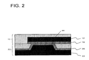
- FIG. 2 is a cross-sectional view showing a portion around an interface between the first interconnect layer and the second interconnect layer;
- FIGS. 3A to 3E are schematic cross-sectional views for explaining a method of manufacturing the semiconductor device according to the first embodiment
- FIGS. 4A and 4B are schematic cross-sectional views for explaining a method of manufacturing the semiconductor device according to the first embodiment
- FIGS. 5A and 5B are schematic cross-sectional views for explaining a method of manufacturing the semiconductor device according to the first embodiment
- FIGS. 6A and 6B are schematic cross-sectional views for explaining a method of manufacturing the semiconductor device according to the first embodiment
- FIGS. 7A and 7B are schematic cross-sectional views for explaining a method of manufacturing the semiconductor device according to the first embodiment
- FIGS. 8A and 8B are schematic cross-sectional views for explaining a method of manufacturing the semiconductor device according to the first embodiment
- FIG. 9 is a schematic cross-sectional view showing a semiconductor device according to the second embodiment of the present invention.
- FIG. 10 is a schematic cross-sectional view showing a variation of the semiconductor device shown in FIG. 9 ;
- FIG. 11 is a schematic cross-sectional view showing a semiconductor device according to a variation of the embodiments.
- FIG. 12 is a schematic cross-sectional view showing a semiconductor device according to another variation of the embodiments.
- FIG. 13 is a schematic cross-sectional view showing a semiconductor device according to still another variation of the embodiments.
- FIG. 1 is a schematic cross-sectional view showing a semiconductor device according to the first embodiment of the present invention.
- the semiconductor device 1 includes interconnect layers 10 , 20 , an IC chip 30 , via plugs 42 , 44 , a seal resin 50 , and solder balls 60 .
- the IC chip 30 , the interconnect layer 10 and the interconnect layer 20 are stacked in this sequence and electrically connected to one another.
- the IC chip 30 is mounted on a first surface 10 a of the interconnect layer 10
- the interconnect layer 20 is provided on a second surface 10 b of the interconnect layer 10 , opposite to the first surface 10 a.
- the interconnect layer 10 (first interconnect layer) includes a conductor interconnect 12 (first interconnect) and an insulating resin 14 .
- the conductor interconnect 12 is buried in a part of the surface layer of the insulating resin 14 facing the interconnect layer 20 .
- Examples of a conductive material employed as the conductor interconnect 12 include Cu, Ni, Au, and Ag.
- the insulating resin 14 may be a PBO (polybenzooxazole) or a polyimide resin.
- the polyimide resin may be photosensitive or non-photosensitive.
- the interconnect layer 10 also includes the via plug 42 (first conductive plug).
- the via plug 42 extends from the conductor interconnect 12 to the first surface 10 a . Accordingly, an end of the via plug 42 is connected to the conductor interconnect 12 , and the other end is exposed on the first surface 10 a of the interconnect layer 10 . Also, as is apparent from FIG. 1 , the end face of the via plug 42 on the side of the interconnect layer 20 is smaller in area than the opposite end face, i.e. the end face on the side of the IC chip 30 .
- the via plug 42 serves to electrically connect the interconnect layer 10 and the IC chip 30 .
- the interconnect layer 20 (second interconnect layer) includes a conductor interconnect 22 (second interconnect) and an insulating resin 24 .
- the conductor interconnect 22 is buried in the insulating resin 24 .
- Examples of a conductive material employed as the conductor interconnect 12 include Cu, Ni, Au, and Ag.
- the insulating resin 24 may be a non-photosensitive resin such as an epoxy resin.
- the interconnect structure constituted of the interconnect layer 10 and the interconnect layer 20 serves as an interposer in the semiconductor device 1 .
- the thermal decomposition temperature of the insulating resin 14 constituting the interconnect layer 10 is higher than that of the insulating resin 24 constituting the interconnect layer 20 .
- the thermal decomposition temperature is 540 degree centigrade or so.
- the thermal decomposition temperature is 310 degree centigrade or so.
- the thermal decomposition temperature herein refers to a temperature at which the weight of the resin is reduced by 5 wt. %, when measured by a thermo balance at a heating speed of 10 degree centigrade per minute.
- the interconnect layer 20 also includes the via plug 44 (second conductive plug).
- the via plug 44 extends from the conductor interconnect 12 to the conductor interconnect 22 . Accordingly, an end of the via plug 44 is connected to the conductor interconnect 12 , and the other end is connected to the conductor interconnect 22 . Also, as is apparent from FIG. 1 , the end face of the via plug 44 on the side of the interconnect layer 10 is smaller in area than the opposite end face, i.e. the end face on the side of the solder balls 60 .
- the via plug 44 serves to electrically connect the interconnect layer 10 and the interconnect layer 20 .
- the minimum interval between the via plugs 42 is narrower than the minimum interval between the via plugs 44 .
- the interval between the via plugs herein refers to a distance between a center line (straight line passing through the center of the both end faces of the via plug) of the respective via plugs. Accordingly, the minimum interval between the via plugs means the interval between two closest via plugs.
- the IC chip 30 (semiconductor chip) is mounted by flip-chip bonding on the first surface 10 a of the interconnect layer 10 . More specifically, the IC chip 30 is fixed to the interconnect layer 10 by solder balls 32 connected to the via plug 42 . Between the interconnect layer 10 and the IC chip 30 , an underfill resin 34 is provided.
- a seal resin 50 is provided so as to cover a side face of the IC chip 30 .
- the seal resin 50 covers not only the side face of the IC chip 30 , but also the upper surface thereof (surface opposite to the interconnect layer 10 ).
- solder balls 60 are connected to the surface of the interconnect layer 20 opposite to the interconnect layer 10 .
- the solder balls 60 are respectively connected to the conductor interconnect 22 at an end portion. Accordingly, a portion of each solder ball 60 is buried in the interconnect layer 20 .
- the solder balls 60 serve as an external connection terminal of the semiconductor device 1 .
- an adhesion metal film 16 is provided on the surface of the conductor interconnect 12 facing the interconnect layer 20 .
- Another adhesion metal film 26 is provided on the surface of the conductor interconnect 22 facing the interconnect layer 10 .
- the adhesion metal film 26 is disposed so as to cover the via plug 44 .
- the adhesion metal film 16 and the adhesion metal film 26 are in mutual contact on the via plug 44 .
- the adhesion metal film 16 is, for instance, a Ni film.
- the adhesion metal film 26 is, for instance, a multilayer metal film (Ti/Ni film) constituted of a Ti film provided on the side of the interconnect layer 10 and a Ni film provided on the side of the conductor interconnect 22 .
- FIGS. 3A through 8B detailed description will be given on a method of manufacturing the semiconductor device 1 , which corresponds to the first embodiment of the method of manufacturing the semiconductor device according to the present invention. Prior to the detailed description, an outline of the manufacturing method according to this embodiment will be described referring to FIGS. 3A to 3E .
- the interconnect layer 10 is formed on a supporting substrate 90 (first interconnect layer formation step).
- the supporting substrate 90 is a silicon substrate.
- the IC chip 30 is mounted on the first surface 10 a of the interconnect layer 10 (semiconductor chip mounting step). Then as shown in FIG. 3C , the seal resin 50 is provided on the interconnect layer 10 so as to cover the side face of the IC chip 30 (seal resin formation step).
- FIG. 3D shows a state that the supporting substrate 90 has been removed (supporting substrate removal step).
- the interconnect layer 20 is formed on the second surface 10 b of the interconnect layer 10 (second interconnect layer formation step). Finally, though not shown in the drawing, the solder balls 60 are formed, thereby completing the manufacturing of the semiconductor device 1 shown in FIG. 1 .
- the first interconnect layer formation step includes the first interconnect formation step and the first conductive plug formation step, which will be subsequently described
- the second interconnect layer formation step includes the second conductive plug formation step and the second interconnect formation step to be subsequently described.
- a resin having a lower thermal decomposition temperature is employed as the insulating resin 24 constituting the interconnect layer 20 , than a resin employed in the first interconnect layer formation step as the insulating resin 14 constituting the interconnect layer 10 .
- a metal thin film 92 which serves as a seed metal for plating, is formed on the supporting substrate 90 by sputtering or the like ( FIG. 4A ).
- a pattern is delineated by photolithography for example.
- plating is performed utilizing the seed metal layer as a feeding layer, to form a conductor pattern which is to constitute the conductor interconnect 12 (first interconnect formation step) ( FIG. 4B ).
- the insulating resin 14 is provided so as to cover the conductor interconnect 12 that has just been formed. Then a via hole 43 is formed by photolithography or the like at a predetermined position of the insulating resin 14 , where the via plug 42 is to be formed ( FIG. 5A ). Then plating is performed to fill the via hole 43 utilizing the seed metal layer as a feeding layer, thus to form the via plug 42 (first conductive plug formation step). At this stage, the interconnect layer 10 is obtained on the supporting substrate 90 ( FIG. 5B ).
- electrodes (solder balls 32 ) of the IC chip 30 are connected to the via plug 42 on the supporting substrate 90 , at a fine pitch.
- the region between the IC chip 30 and the interconnect layer 10 is filled with the underfill resin 34 , which is then cured ( FIG. 6A ).
- the seal resin 50 is provided on the interconnect layer 10 so as to cover the IC chip 30 .
- interconnect layer 10 and the side face of the IC chip 30 are covered with the seal resin 50 ( FIG. 6B ).
- the supporting substrate 90 is removed, and etching is performed to remove the metal thin film 92 ( FIG. 7A ).
- a portion of the insulating resin 24 is provided on the second surface 10 b of the interconnect layer 10 , now exposed because of the above removal.
- a via hole 45 is formed with a laser or the like, at a predetermined position of the insulating resin 24 where the via plug 44 is to be formed ( FIG. 7B ).
- the via plug 44 is then formed in the via hole 45 (second conductive plug formation step).
- a conductor pattern which is to constitute the conductor interconnect 22 is formed on the insulating resin 24 that has been halfway formed (second interconnect formation step) ( FIG. 8A ).
- the insulating resin 24 is fully formed.
- This process also includes forming openings 61 for the solder balls 60 at predetermined positions of the insulating resin 24 .
- the interconnect layer 20 is obtained on the interconnect layer 10 ( FIG. 8B ).
- the solder balls 60 are formed so as to fill in the openings 61 , thereby completing the manufacturing of the semiconductor device 1 shown in FIG. 1 .
- the interconnect layers 10 , 20 are built up in an upward and downward direction respectively, in the relevant drawings. Accordingly, the end face of the via plug 42 on the side of the IC chip 30 is larger in area than the end face thereof on the side of the interconnect layer 20 , and the end face of the via plug 44 on the side of the solder balls 60 is larger in area than the end face thereof on the side of the interconnect layer 10 .
- This embodiment offers the following advantageous effects.
- the foregoing method of manufacturing includes forming the interconnect layer 10 , on which the IC chip 30 is to be mounted, on the supporting substrate 90 , while forming the interconnect layer 20 after the removal of the supporting substrate 90 .
- Such method removes the restriction against the use of a resin having a lower thermal decomposition temperature than the insulating resin 14 , as the insulating resin 24 . Therefore, the method allows employing a resin appropriate for fine-scale processing as the insulating resin 14 , while employing a relatively inexpensive resin as the insulating resin 24 .
- the foregoing embodiment provides a method of manufacturing the semiconductor device 1 that can be manufactured at a lower cost, yet allows achieving fine-scale connection between the interconnect layer 10 and the IC chip 30 .
- the interconnect pattern of the conductor interconnect 12 is formed on the sufficiently rigid supporting substrate 90 , which permits the formation of the conductor interconnect 12 in a fine pattern. Also, since the interconnect layer 10 and the IC chip 30 are bonded on the supporting substrate 90 , the interconnect layer 10 and the IC chip 30 can be connected via the bumps at a fine pitch. This leads to reduction in the number of the interconnect layers, as well as in dimensions of the IC chip 30 .
- the insulating resin 24 constituting the interconnect layer 20 can be made thicker than the insulating resin 14 , because the interconnect layer 20 is formed after the removal of the supporting substrate 90 . This enhances the stress relief performance of the insulating resin 24 , thus resulting in upgraded reliability of the semiconductor device 1 .
- a resin having a lower thermal decomposition temperature than the insulating resin 14 constituting the interconnect layer 10 formed in the first interconnect layer formation step, is employed as the insulating resin 24 constituting the interconnect layer 20 .
- Such arrangement allows properly forming the interconnect layer 20 on the interconnect layer 10 .
- the first interconnect layer formation step includes the first interconnect formation step and the first conductive plug formation step.
- the second interconnect layer formation step includes the second conductive plug formation step and the second interconnect formation step.
- the semiconductor device 1 a resin having a lower thermal decomposition temperature than the insulating resin 14 constituting the interconnect layer 10 can be employed as the insulating resin 24 constituting the interconnect layer 20 . Accordingly, the semiconductor device 1 allows employing a resin appropriate for fine-scale processing as the insulating resin 14 , while employing a relatively inexpensive resin as the insulating resin 24 . Thus, the semiconductor device 1 can be manufactured at a lower cost, yet allows achieving fine-scale connection between the interconnect layer 10 and the IC chip 30 .
- the interconnect layer 10 and the interconnect layer 20 are in direct contact with each other, without intermediation by a core layer.
- a via plug formed in the core layer is generally more difficult to micronize than a via plug formed in an ordinary interconnect layer, and hence may restrain the micronization of the semiconductor device as a whole.
- the semiconductor device 1 does not include any core layer, the semiconductor device 1 can remain free from such problem.
- the interconnect layers 10 , 20 respectively include the conductor interconnects 12 , 22 .
- the via plug 42 extends from the conductor interconnect 12 to the first surface 10 a of the interconnect layer 10 , while the via plug extends from the conductor interconnect 12 to the conductor interconnect 22 .
- Such configuration achieves the semiconductor device 1 that includes a multilayer interconnect structure including the conductor interconnects 12 , 22 .
- the seal resin 50 is provided so as to cover the side face of the IC chip 30 . This assures that the physical structure of the interconnect layers is maintained even after the removal of the supporting substrate 90 . Accordingly, the solder balls 60 can be formed with high coplanarity. Here, providing the seal resin 50 (and the seal resin formation step) is not imperative.
- a silicon substrate is employed as the supporting substrate 90 . Accordingly, impact of thermal expansion can be reduced, in comparison with an insulating substrate. This facilitates further micronization in the connection of the interconnect layer 10 and the IC chip 30 .
- the minimum interval between the via plugs 42 is narrower than the minimum interval between the via plugs 44 .
- a resin appropriate for fine-scale processing should be employed as the insulating resin 14 , it is not necessary to employ such a resin as the insulating resin 24 . Accordingly, a relatively inexpensive resin such as an epoxy resin may be employed as the insulating resin 24 .
- a PBO or a polyimide resin as the insulating resin 14 results in formation of the insulating resin 14 appropriate for fine-scale processing.
- employing the epoxy resin as the insulating resin 24 leads to formation of the insulating resin 24 at a low cost.
- the adhesion metal film 16 is provided on the surface of the conductor interconnect 12 on the side of the interconnect layer 20 .
- the adhesion metal film 26 is provided on the surface of the conductor interconnect 22 on the side of the interconnect layer 10 (Ref. FIG. 2 ).
- Such configuration causes the resin between the conductor interconnect 12 and the conductor interconnect 22 to be held by the adhesion metal films 16 , 26 , thereby achieving firm adhesion between the resin and the conductor interconnects 12 , 22 . This leads to higher reliability of the semiconductor device 1 .
- providing the adhesion metal films 16 , 26 is not imperative.
- the adhesion metal film 26 is provided so as to cover the via plug 44 , thus to be in contact with the adhesion metal film 16 on the via plug 44 . Such direct contact between the adhesion metal films 16 , 26 achieves firm adhesion between the interconnect layer 10 and the interconnect layer 20 .
- the adhesion effect to the resin is further enhanced.
- FIG. 9 is a schematic cross-sectional view showing a semiconductor device according to the second embodiment of the present invention.
- the semiconductor device 2 includes interconnect layers 10 , 70 , an IC chip 30 , via plugs 42 , 46 , a seal resin 50 , and solder balls 62 , among which the interconnect layer 10 , the IC chip 30 , the via plug 42 and the seal resin 50 are of the similar structure to those described referring to FIG. 1 .
- the IC chip 30 , the interconnect layer 10 and the interconnect layer 70 are stacked in this sequence, and electrically connected to one another.
- the interconnect layer 70 (second interconnect layer) includes an insulating resin 74 .
- the interconnect layer 70 is different from the interconnect layer 20 shown in FIG. 1 in not including the conductor interconnect.
- the insulating resin 74 is constituted of a resin having a lower thermal decomposition temperature than the insulating resin 14 .
- the interconnect layer 70 includes the via plug 46 (second conductive plug).
- the via plug 46 corresponds to a portion of the solder ball 62 to be subsequently described, specifically the portion of the solder ball 62 buried in the insulating resin 74 .
- the via plug 46 extends from the conductor interconnect 12 to a surface 70 a of the interconnect layer 70 opposite to the interconnect layer 10 . Also, as is apparent from FIG. 9 , the end face of the via plug 46 on the side of the interconnect layer 10 is smaller in area than the opposite end face.
- the solder balls 62 are connected to the face of the interconnect layer 70 opposite to the interconnect layer 10 . More specifically, the solder balls 62 penetrate through the interconnect layer 70 , so that an end portion thereof is connected to the conductor interconnect 12 . Accordingly, a portion of the solder ball 62 is buried in the interconnect layer 70 , thus constituting the via plug 46 .
- the remaining portion of the solder ball 62 i.e. the portion protruding out of the interconnect layer 70 constitutes a bump in the semiconductor device 2 .
- the bump is provided on the side of the via plug 46 opposite to the interconnect layer 10 , in a body with the via plug 46 .
- the via plug 46 and the bump are constituted of an identical metal material.
- the bump serves as an external connection terminal of the semiconductor device 2 .
- a method of manufacturing the semiconductor device 2 thus configured includes a first interconnect layer formation step, a semiconductor chip mounting step, a seal resin formation step, a supporting substrate removal step and a second interconnect layer formation step.
- the execution sequence of these steps is similar to that of the manufacturing method described referring to FIGS. 3A to 8B .
- actual processes in the first interconnect layer formation step, the semiconductor chip mounting step, the seal resin formation step and the supporting substrate removal step among these steps are similar to those of the manufacturing method described referring to FIGS. 3A to 8B .
- the insulating resin 74 is provided on the interconnect layer 10 (Ref. FIG. 7A ) exposed upon removal of the supporting substrate 90 .
- This process also includes forming openings for the solder balls 62 at predetermined positions of the insulating resin 74 .
- the interconnect layer 70 is obtained on the interconnect layer 10 .
- the via plug 46 is obtained (second conductive plug formation step).
- the bumps are simultaneously formed with the via plug 46 .
- the second conductive plug formation step includes forming the bumps on the opposite side of the via plug 46 to the interconnect layer 10 .
- each of the via plugs 46 and the bumps are integrally formed. That is how the semiconductor device 2 shown in FIG. 9 is obtained.
- the second interconnect layer formation step according to this embodiment only includes the former, out of the second conductive plug formation step and the second interconnect formation step.
- the first interconnect layer formation step includes the first interconnect formation step and the first conductive plug formation step.
- the second interconnect layer formation step includes the second conductive plug formation step.
- the interconnect layer 10 includes the conductor interconnect 12 .
- the via plug 42 extends from the conductor interconnect 12 to the first surface 10 a of the interconnect layer 10
- the via plug 46 extends from the conductor interconnect 12 to the surface 70 a of the interconnect layer 70 .
- Such configuration eliminates the need to form the conductor interconnect in the interconnect layer 70 , thereby permitting use of a resin merely intended for the function of solder resist, as the insulating resin 74 .
- an UBM (Under Bump Metal) 63 may be provided as shown in FIG. 10 .
- the UBM 63 is located between the conductor interconnect 12 and the solder ball 62 .
- the UBM 63 penetrates through the interconnect layer 70 , thus to be connected to the conductor interconnect 12 . Accordingly, a portion of the UBM 63 is buried in the interconnect layer 70 , thus constituting the second conductive plug. Then, the solder ball 62 is formed on the UBM 63 .
- the semiconductor device and the method of manufacturing the same according to the present invention are not limited to the foregoing embodiments, but may be modified in various manners.
- a plurality of IC chips 30 may be provided on the interconnect layer 10 , as shown in FIG. 11 .
- an IC chip 80 may be provided on the interconnect layer 20 , as a second semiconductor chip.
- the IC chip 80 is mounted by flip-chip bonding on the interconnect layer 20 via solder balls 82 connected to the conductor interconnect 22 .
- a plurality of IC chips 30 may be stacked on the interconnect layer 10 .
- the IC chips 30 are stacked in four levels.
- the lowermost IC chip 30 is bonded to the interconnect layer 10 via solder balls 32 .
- the respective IC chips 30 except the topmost one include via plugs 36 .
- the via plug 36 are provided all the way through the respective IC chips 30 .
- the IC chips 30 are connected to one another via solder balls 38 . In other words, the IC chips 30 are electrically connected to one another through the via plugs 36 and the solder balls 38 .
- FIGS. 12 and 13 may be combined. Specifically, the IC chip 80 (Ref. FIG. 12 ) may be provided on the interconnect layer 20 , with a plurality of IC chip 30 (Ref. FIG. 13 ) stacked on the interconnect layer 10 .
- an electronic component other than the IC chip such as a passive component
- a passive component may be provided on the interconnect layers 10 , 20 , 70 .
- the passive component include a capacitor, an inductor, a resistor and so forth.
- the insulating resins 14 , 24 , 74 may be composed of a plurality of types of resins.
- the condition that the thermal decomposition temperature of the insulating resin 14 should be higher than that of the insulating resin 24 is synonymous to the condition that the thermal decomposition temperature of a resin having the lowest thermal decomposition temperature among those constituting the insulating resin 14 should be higher than that of a resin having the highest thermal decomposition temperature among those constituting the insulating resin 24 .
Abstract
Description
Claims (5)
Priority Applications (1)
| Application Number | Priority Date | Filing Date | Title |
|---|---|---|---|
| US12/114,238 US8035231B2 (en) | 2005-04-06 | 2008-05-02 | Semiconductor device and method of manufacturing the same |
Applications Claiming Priority (2)
| Application Number | Priority Date | Filing Date | Title |
|---|---|---|---|
| JP2005109993A JP4790297B2 (en) | 2005-04-06 | 2005-04-06 | Semiconductor device and manufacturing method thereof |
| JP2005-109993 | 2005-04-06 |
Related Child Applications (1)
| Application Number | Title | Priority Date | Filing Date |
|---|---|---|---|
| US12/114,238 Division US8035231B2 (en) | 2005-04-06 | 2008-05-02 | Semiconductor device and method of manufacturing the same |
Publications (2)
| Publication Number | Publication Date |
|---|---|
| US20060226556A1 US20060226556A1 (en) | 2006-10-12 |
| US7927999B2 true US7927999B2 (en) | 2011-04-19 |
Family
ID=37082430
Family Applications (2)
| Application Number | Title | Priority Date | Filing Date |
|---|---|---|---|
| US11/393,686 Active 2027-05-27 US7927999B2 (en) | 2005-04-06 | 2006-03-31 | Method of forming metal interconnect layers for flip chip device |
| US12/114,238 Active 2027-09-29 US8035231B2 (en) | 2005-04-06 | 2008-05-02 | Semiconductor device and method of manufacturing the same |
Family Applications After (1)
| Application Number | Title | Priority Date | Filing Date |
|---|---|---|---|
| US12/114,238 Active 2027-09-29 US8035231B2 (en) | 2005-04-06 | 2008-05-02 | Semiconductor device and method of manufacturing the same |
Country Status (2)
| Country | Link |
|---|---|
| US (2) | US7927999B2 (en) |
| JP (1) | JP4790297B2 (en) |
Cited By (1)
| Publication number | Priority date | Publication date | Assignee | Title |
|---|---|---|---|---|
| US20180233478A1 (en) * | 2014-12-04 | 2018-08-16 | Siliconware Precision Industries Co., Ltd. | Method of fabricating packaging structure |
Families Citing this family (45)
| Publication number | Priority date | Publication date | Assignee | Title |
|---|---|---|---|---|
| JP4790297B2 (en) * | 2005-04-06 | 2011-10-12 | ルネサスエレクトロニクス株式会社 | Semiconductor device and manufacturing method thereof |
| JP2008091639A (en) * | 2006-10-02 | 2008-04-17 | Nec Electronics Corp | Electronic equipment, and manufacturing method thereof |
| JP4897451B2 (en) * | 2006-12-04 | 2012-03-14 | ルネサスエレクトロニクス株式会社 | Semiconductor device |
| US7767496B2 (en) | 2007-12-14 | 2010-08-03 | Stats Chippac, Ltd. | Semiconductor device and method of forming interconnect structure for encapsulated die having pre-applied protective layer |
| US8183095B2 (en) | 2010-03-12 | 2012-05-22 | Stats Chippac, Ltd. | Semiconductor device and method of forming sacrificial protective layer to protect semiconductor die edge during singulation |
| US9318441B2 (en) | 2007-12-14 | 2016-04-19 | Stats Chippac, Ltd. | Semiconductor device and method of forming sacrificial adhesive over contact pads of semiconductor die |
| US8343809B2 (en) * | 2010-03-15 | 2013-01-01 | Stats Chippac, Ltd. | Semiconductor device and method of forming repassivation layer with reduced opening to contact pad of semiconductor die |
| US8456002B2 (en) | 2007-12-14 | 2013-06-04 | Stats Chippac Ltd. | Semiconductor device and method of forming insulating layer disposed over the semiconductor die for stress relief |
| WO2009084300A1 (en) | 2007-12-28 | 2009-07-09 | Ibiden Co., Ltd. | Interposer and manufacturing method of the interposer |
| CN101632168B (en) | 2007-12-28 | 2012-07-18 | 揖斐电株式会社 | Interposer and interposer manufacturing method |
| US7952160B2 (en) * | 2007-12-31 | 2011-05-31 | Intel Corporation | Packaged voltage regulator and inductor array |
| US8552570B2 (en) | 2008-01-09 | 2013-10-08 | Renesas Electronics Corporation | Wiring board, semiconductor device, and method for manufacturing wiring board and semiconductor device |
| US9675443B2 (en) | 2009-09-10 | 2017-06-13 | Johnson & Johnson Vision Care, Inc. | Energized ophthalmic lens including stacked integrated components |
| EP2178113A1 (en) * | 2008-10-15 | 2010-04-21 | Nxp B.V. | Electronic component and method of manufacturing the same |
| JP2010245383A (en) | 2009-04-08 | 2010-10-28 | Elpida Memory Inc | Semiconductor device and method of manufacturing the same |
| JP5715334B2 (en) * | 2009-10-15 | 2015-05-07 | ルネサスエレクトロニクス株式会社 | Semiconductor device |
| US9548240B2 (en) | 2010-03-15 | 2017-01-17 | STATS ChipPAC Pte. Ltd. | Semiconductor device and method of forming repassivation layer for robust low cost fan-out semiconductor package |
| US8298863B2 (en) * | 2010-04-29 | 2012-10-30 | Texas Instruments Incorporated | TCE compensation for package substrates for reduced die warpage assembly |
| US8716873B2 (en) | 2010-07-01 | 2014-05-06 | United Test And Assembly Center Ltd. | Semiconductor packages and methods of packaging semiconductor devices |
| US9059187B2 (en) | 2010-09-30 | 2015-06-16 | Ibiden Co., Ltd. | Electronic component having encapsulated wiring board and method for manufacturing the same |
| US8698303B2 (en) * | 2010-11-23 | 2014-04-15 | Ibiden Co., Ltd. | Substrate for mounting semiconductor, semiconductor device and method for manufacturing semiconductor device |
| US8950862B2 (en) | 2011-02-28 | 2015-02-10 | Johnson & Johnson Vision Care, Inc. | Methods and apparatus for an ophthalmic lens with functional insert layers |
| US9698129B2 (en) * | 2011-03-18 | 2017-07-04 | Johnson & Johnson Vision Care, Inc. | Stacked integrated component devices with energization |
| US10451897B2 (en) | 2011-03-18 | 2019-10-22 | Johnson & Johnson Vision Care, Inc. | Components with multiple energization elements for biomedical devices |
| US9889615B2 (en) | 2011-03-18 | 2018-02-13 | Johnson & Johnson Vision Care, Inc. | Stacked integrated component media insert for an ophthalmic device |
| US9110310B2 (en) * | 2011-03-18 | 2015-08-18 | Johnson & Johnson Vision Care, Inc. | Multiple energization elements in stacked integrated component devices |
| US9804418B2 (en) | 2011-03-21 | 2017-10-31 | Johnson & Johnson Vision Care, Inc. | Methods and apparatus for functional insert with power layer |
| US8857983B2 (en) | 2012-01-26 | 2014-10-14 | Johnson & Johnson Vision Care, Inc. | Ophthalmic lens assembly having an integrated antenna structure |
| KR101411813B1 (en) * | 2012-11-09 | 2014-06-27 | 앰코 테크놀로지 코리아 주식회사 | Semiconductor device and manufacturing method thereof |
| US9799592B2 (en) | 2013-11-19 | 2017-10-24 | Amkor Technology, Inc. | Semicondutor device with through-silicon via-less deep wells |
| TWI616979B (en) * | 2014-03-14 | 2018-03-01 | Toshiba Memory Corp | Semiconductor device and manufacturing method thereof |
| JP6259737B2 (en) * | 2014-03-14 | 2018-01-10 | 東芝メモリ株式会社 | Semiconductor device and manufacturing method thereof |
| US9418877B2 (en) * | 2014-05-05 | 2016-08-16 | Qualcomm Incorporated | Integrated device comprising high density interconnects in inorganic layers and redistribution layers in organic layers |
| US9793536B2 (en) | 2014-08-21 | 2017-10-17 | Johnson & Johnson Vision Care, Inc. | Pellet form cathode for use in a biocompatible battery |
| US10627651B2 (en) | 2014-08-21 | 2020-04-21 | Johnson & Johnson Vision Care, Inc. | Methods and apparatus to form biocompatible energization primary elements for biomedical devices with electroless sealing layers |
| US9383593B2 (en) | 2014-08-21 | 2016-07-05 | Johnson & Johnson Vision Care, Inc. | Methods to form biocompatible energization elements for biomedical devices comprising laminates and placed separators |
| US9715130B2 (en) | 2014-08-21 | 2017-07-25 | Johnson & Johnson Vision Care, Inc. | Methods and apparatus to form separators for biocompatible energization elements for biomedical devices |
| US10361405B2 (en) | 2014-08-21 | 2019-07-23 | Johnson & Johnson Vision Care, Inc. | Biomedical energization elements with polymer electrolytes |
| US10381687B2 (en) | 2014-08-21 | 2019-08-13 | Johnson & Johnson Vision Care, Inc. | Methods of forming biocompatible rechargable energization elements for biomedical devices |
| US9599842B2 (en) | 2014-08-21 | 2017-03-21 | Johnson & Johnson Vision Care, Inc. | Device and methods for sealing and encapsulation for biocompatible energization elements |
| US10361404B2 (en) | 2014-08-21 | 2019-07-23 | Johnson & Johnson Vision Care, Inc. | Anodes for use in biocompatible energization elements |
| US9941547B2 (en) | 2014-08-21 | 2018-04-10 | Johnson & Johnson Vision Care, Inc. | Biomedical energization elements with polymer electrolytes and cavity structures |
| TW201637139A (en) * | 2015-04-14 | 2016-10-16 | 矽品精密工業股份有限公司 | Electronic package structure and method of fabricating the same |
| US10345620B2 (en) | 2016-02-18 | 2019-07-09 | Johnson & Johnson Vision Care, Inc. | Methods and apparatus to form biocompatible energization elements incorporating fuel cells for biomedical devices |
| US10504827B2 (en) * | 2016-06-03 | 2019-12-10 | Amkor Technology, Inc. | Semiconductor device and manufacturing method thereof |
Citations (30)
| Publication number | Priority date | Publication date | Assignee | Title |
|---|---|---|---|---|
| US4497864A (en) * | 1982-07-06 | 1985-02-05 | Fuji Photo Film Co., Ltd. | Magnetic recording medium |
| JPS62229899A (en) | 1986-03-29 | 1987-10-08 | 京セラ株式会社 | Plug-in type multilayer interconnection board |
| US4788097A (en) * | 1986-02-12 | 1988-11-29 | Fuji Photo Film Co., Ltd. | Information recording medium |
| JPH01143394A (en) | 1987-11-30 | 1989-06-05 | Ngk Insulators Ltd | Ceramic package with lead |
| US4861854A (en) * | 1986-02-03 | 1989-08-29 | Mitsubishi Gas Chemical Company, Inc. | Photosensitive polyimide precursor |
| US5284899A (en) * | 1991-09-09 | 1994-02-08 | Sumitomo Bakelite Company Limited | Resin paste for tight sealing |
| WO1996019829A1 (en) | 1994-12-22 | 1996-06-27 | Pace Benedict G | Device for superheating steam |
| JPH11126978A (en) * | 1997-10-24 | 1999-05-11 | Kyocera Corp | Multilayered wiring board |
| JP2001177010A (en) * | 1999-10-05 | 2001-06-29 | Nec Corp | Wiring board, semiconductor device having wiring board and manufacturing method thereof and packaging method |
| US20020054471A1 (en) * | 2000-08-30 | 2002-05-09 | International Business Machines Corporation | Method of making a parallel capacitor laminate |
| US6406942B2 (en) * | 2000-03-09 | 2002-06-18 | Nec Corporation | Flip chip type semiconductor device and method for manufacturing the same |
| JP2002343931A (en) | 2001-05-17 | 2002-11-29 | Hitachi Ltd | Wiring board, manufacturing method thereof, multi-chip module, manufacturing method thereof, and multi-chip module mounting structure body |
| US20030202142A1 (en) * | 2002-04-26 | 2003-10-30 | Hitachi Displays, Ltd. | Liquid crystal display device and fabrication method thereof |
| JP2003309215A (en) | 2002-02-15 | 2003-10-31 | Nec Electronics Corp | Semiconductor device and method of manufacturing the same |
| US20030230813A1 (en) * | 2001-06-07 | 2003-12-18 | Matsushita Electric Industrial Co., Ltd. | Method for manufacturing circuit board and circuit board and power conversion module using the same |
| JP2004039867A (en) | 2002-07-03 | 2004-02-05 | Sony Corp | Multilayer wiring circuit module and its manufacturing method |
| US20040090756A1 (en) * | 2002-11-07 | 2004-05-13 | Kwun-Yo Ho | Chip packaging structure and manufacturing process thereof |
| JP2004265967A (en) | 2003-02-28 | 2004-09-24 | Nec Toppan Circuit Solutions Inc | Multilayer printed wiring board, its manufacturing method and semiconductor device |
| JP2005063987A (en) | 2003-08-08 | 2005-03-10 | Ngk Spark Plug Co Ltd | Wiring board and its manufacturing method |
| US20050056942A1 (en) * | 2003-09-15 | 2005-03-17 | International Business Machines Corporation | Method of fabricating integrated electronic chip with an interconnect device |
| US6902950B2 (en) * | 2000-10-18 | 2005-06-07 | Intel Corporation | Method to protect an encapsulated die package during back grinding with a solder metallization layer and devices formed thereby |
| US20060043570A1 (en) * | 2004-08-25 | 2006-03-02 | Shigetsugu Muramatsu | Substrate, semiconductor device, substrate fabricating method, and semiconductor device fabricating method |
| US20060226556A1 (en) * | 2005-04-06 | 2006-10-12 | Nec Electronics Corporation | Semiconductor device and method of manufacturing the same |
| US20070026662A1 (en) * | 2005-07-26 | 2007-02-01 | Nec Electronics Corporation | Semiconductor device and method of manufacturing the same |
| US20070169886A1 (en) * | 2004-03-04 | 2007-07-26 | Toray Industries, Inc. | Heat-resistant resin laminated film, multilayer film with metal layer including same and semiconductor device |
| US20070241464A1 (en) * | 2004-11-10 | 2007-10-18 | Stats Chippac Ltd. | Solder joint flip chip interconnection having relief structure |
| US20080079163A1 (en) * | 2006-10-02 | 2008-04-03 | Nec Electronics Corporation | Electronic device and method of manufacturing the same |
| US7452797B2 (en) * | 2003-04-15 | 2008-11-18 | Harima Chemicals, Inc. | Solder deposition method and solder bump forming method |
| US20080312383A1 (en) * | 2002-03-08 | 2008-12-18 | Kaneka Corporation | Thermosetting Resin Composition, And Laminate and Circuit Substrate Using Same |
| US20090008765A1 (en) * | 2005-12-14 | 2009-01-08 | Takaharu Yamano | Chip embedded substrate and method of producing the same |
Family Cites Families (15)
| Publication number | Priority date | Publication date | Assignee | Title |
|---|---|---|---|---|
| DE59702929D1 (en) * | 1996-07-31 | 2001-02-22 | Dyconex Patente Zug | METHOD FOR PRODUCING CONNECTION LADDERS |
| DE69936892T2 (en) * | 1998-02-26 | 2007-12-06 | Ibiden Co., Ltd., Ogaki | Multilayer printed circuit board with filled contact holes |
| US7405149B1 (en) * | 1998-12-21 | 2008-07-29 | Megica Corporation | Post passivation method for semiconductor chip or wafer |
| US20090111206A1 (en) * | 1999-03-30 | 2009-04-30 | Daniel Luch | Collector grid, electrode structures and interrconnect structures for photovoltaic arrays and methods of manufacture |
| EP1194022B1 (en) * | 1999-06-02 | 2006-11-02 | Ibiden Co., Ltd. | Multilayer printed wiring board and method of manufacturing multilayer printed wiring board |
| TW512653B (en) * | 1999-11-26 | 2002-12-01 | Ibiden Co Ltd | Multilayer circuit board and semiconductor device |
| JP3979791B2 (en) * | 2000-03-08 | 2007-09-19 | 株式会社ルネサステクノロジ | Semiconductor device and manufacturing method thereof |
| JP3537400B2 (en) * | 2000-03-17 | 2004-06-14 | 松下電器産業株式会社 | Semiconductor built-in module and method of manufacturing the same |
| JP2002343923A (en) * | 2001-05-17 | 2002-11-29 | Hitachi Maxell Ltd | Semiconductor module and manufacturing method therefor |
| EP1418619A4 (en) * | 2001-08-13 | 2010-09-08 | Ebara Corp | Semiconductor device and production method therefor, and plating solution |
| JP3861669B2 (en) * | 2001-11-22 | 2006-12-20 | ソニー株式会社 | Manufacturing method of multichip circuit module |
| JP4045143B2 (en) * | 2002-02-18 | 2008-02-13 | テセラ・インターコネクト・マテリアルズ,インコーポレイテッド | Manufacturing method of wiring film connecting member and manufacturing method of multilayer wiring board |
| JP2003273509A (en) * | 2002-03-14 | 2003-09-26 | Fujitsu Ltd | Wiring board and its manufacturing method |
| JP2005072328A (en) * | 2003-08-26 | 2005-03-17 | Kyocera Corp | Multilayer wiring board |
| JP4551730B2 (en) * | 2004-10-15 | 2010-09-29 | イビデン株式会社 | Multilayer core substrate and manufacturing method thereof |
-
2005
- 2005-04-06 JP JP2005109993A patent/JP4790297B2/en not_active Expired - Fee Related
-
2006
- 2006-03-31 US US11/393,686 patent/US7927999B2/en active Active
-
2008
- 2008-05-02 US US12/114,238 patent/US8035231B2/en active Active
Patent Citations (32)
| Publication number | Priority date | Publication date | Assignee | Title |
|---|---|---|---|---|
| US4497864A (en) * | 1982-07-06 | 1985-02-05 | Fuji Photo Film Co., Ltd. | Magnetic recording medium |
| US4861854A (en) * | 1986-02-03 | 1989-08-29 | Mitsubishi Gas Chemical Company, Inc. | Photosensitive polyimide precursor |
| US4788097A (en) * | 1986-02-12 | 1988-11-29 | Fuji Photo Film Co., Ltd. | Information recording medium |
| JPS62229899A (en) | 1986-03-29 | 1987-10-08 | 京セラ株式会社 | Plug-in type multilayer interconnection board |
| JPH01143394A (en) | 1987-11-30 | 1989-06-05 | Ngk Insulators Ltd | Ceramic package with lead |
| US5284899A (en) * | 1991-09-09 | 1994-02-08 | Sumitomo Bakelite Company Limited | Resin paste for tight sealing |
| WO1996019829A1 (en) | 1994-12-22 | 1996-06-27 | Pace Benedict G | Device for superheating steam |
| JPH11126978A (en) * | 1997-10-24 | 1999-05-11 | Kyocera Corp | Multilayered wiring board |
| JP2001177010A (en) * | 1999-10-05 | 2001-06-29 | Nec Corp | Wiring board, semiconductor device having wiring board and manufacturing method thereof and packaging method |
| US20070184604A1 (en) * | 1999-10-05 | 2007-08-09 | Nec Electronics Corporation | Multilayer interconnection board, semiconductor device having the same, and method of forming the same as well as method of mounting the semicondutor chip on the interconnection board |
| US6406942B2 (en) * | 2000-03-09 | 2002-06-18 | Nec Corporation | Flip chip type semiconductor device and method for manufacturing the same |
| US20020054471A1 (en) * | 2000-08-30 | 2002-05-09 | International Business Machines Corporation | Method of making a parallel capacitor laminate |
| US6902950B2 (en) * | 2000-10-18 | 2005-06-07 | Intel Corporation | Method to protect an encapsulated die package during back grinding with a solder metallization layer and devices formed thereby |
| JP2002343931A (en) | 2001-05-17 | 2002-11-29 | Hitachi Ltd | Wiring board, manufacturing method thereof, multi-chip module, manufacturing method thereof, and multi-chip module mounting structure body |
| US20030230813A1 (en) * | 2001-06-07 | 2003-12-18 | Matsushita Electric Industrial Co., Ltd. | Method for manufacturing circuit board and circuit board and power conversion module using the same |
| JP2003309215A (en) | 2002-02-15 | 2003-10-31 | Nec Electronics Corp | Semiconductor device and method of manufacturing the same |
| US20080312383A1 (en) * | 2002-03-08 | 2008-12-18 | Kaneka Corporation | Thermosetting Resin Composition, And Laminate and Circuit Substrate Using Same |
| US20030202142A1 (en) * | 2002-04-26 | 2003-10-30 | Hitachi Displays, Ltd. | Liquid crystal display device and fabrication method thereof |
| US6833895B2 (en) * | 2002-04-26 | 2004-12-21 | Hitachi Displays, Ltd. | Liquid crystal display device and fabrication method thereof |
| JP2004039867A (en) | 2002-07-03 | 2004-02-05 | Sony Corp | Multilayer wiring circuit module and its manufacturing method |
| US20040090756A1 (en) * | 2002-11-07 | 2004-05-13 | Kwun-Yo Ho | Chip packaging structure and manufacturing process thereof |
| JP2004265967A (en) | 2003-02-28 | 2004-09-24 | Nec Toppan Circuit Solutions Inc | Multilayer printed wiring board, its manufacturing method and semiconductor device |
| US7452797B2 (en) * | 2003-04-15 | 2008-11-18 | Harima Chemicals, Inc. | Solder deposition method and solder bump forming method |
| JP2005063987A (en) | 2003-08-08 | 2005-03-10 | Ngk Spark Plug Co Ltd | Wiring board and its manufacturing method |
| US20050056942A1 (en) * | 2003-09-15 | 2005-03-17 | International Business Machines Corporation | Method of fabricating integrated electronic chip with an interconnect device |
| US20070169886A1 (en) * | 2004-03-04 | 2007-07-26 | Toray Industries, Inc. | Heat-resistant resin laminated film, multilayer film with metal layer including same and semiconductor device |
| US20060043570A1 (en) * | 2004-08-25 | 2006-03-02 | Shigetsugu Muramatsu | Substrate, semiconductor device, substrate fabricating method, and semiconductor device fabricating method |
| US20070241464A1 (en) * | 2004-11-10 | 2007-10-18 | Stats Chippac Ltd. | Solder joint flip chip interconnection having relief structure |
| US20060226556A1 (en) * | 2005-04-06 | 2006-10-12 | Nec Electronics Corporation | Semiconductor device and method of manufacturing the same |
| US20070026662A1 (en) * | 2005-07-26 | 2007-02-01 | Nec Electronics Corporation | Semiconductor device and method of manufacturing the same |
| US20090008765A1 (en) * | 2005-12-14 | 2009-01-08 | Takaharu Yamano | Chip embedded substrate and method of producing the same |
| US20080079163A1 (en) * | 2006-10-02 | 2008-04-03 | Nec Electronics Corporation | Electronic device and method of manufacturing the same |
Non-Patent Citations (4)
| Title |
|---|
| Japanese Official Action-2005-109993-Sep. 16, 2010. |
| Japanese Official Action—2005-109993—Sep. 16, 2010. |
| Semiconductor OneSource, "Interconnect", http://www.semi1source.com/glossary/default.asp?searchterm=interconnect. * |
| Song, et al. "Thermal Decomposition Characteristics of DGEBA/MDA/GN System for Insulating Materials" Sep. 1998, Proceedings of 1998 International Symposium on Electrical Insulating Materials, p. 286. * |
Cited By (2)
| Publication number | Priority date | Publication date | Assignee | Title |
|---|---|---|---|---|
| US20180233478A1 (en) * | 2014-12-04 | 2018-08-16 | Siliconware Precision Industries Co., Ltd. | Method of fabricating packaging structure |
| US10403596B2 (en) * | 2014-12-04 | 2019-09-03 | Siliconware Precision Indsutries Co., Ltd. | Method of fabricating packaging structure |
Also Published As
| Publication number | Publication date |
|---|---|
| US20060226556A1 (en) | 2006-10-12 |
| US8035231B2 (en) | 2011-10-11 |
| US20080203565A1 (en) | 2008-08-28 |
| JP4790297B2 (en) | 2011-10-12 |
| JP2006294692A (en) | 2006-10-26 |
Similar Documents
| Publication | Publication Date | Title |
|---|---|---|
| US7927999B2 (en) | Method of forming metal interconnect layers for flip chip device | |
| US7670876B2 (en) | Integrated circuit device with embedded passive component by flip-chip connection and method for manufacturing the same | |
| US8685796B2 (en) | Electronic device and method of manufacturing the same | |
| US8823174B2 (en) | Electronic device | |
| US7928001B2 (en) | Electronic device and method of manufacturing the same | |
| US9165878B2 (en) | Semiconductor packages and methods of packaging semiconductor devices | |
| US6908785B2 (en) | Multi-chip package (MCP) with a conductive bar and method for manufacturing the same | |
| CN110085523B (en) | Semiconductor device and method for manufacturing the same | |
| US20040238957A1 (en) | Semiconductor components having multiple on board capacitors | |
| US6587353B2 (en) | Semiconductor device | |
| JP2005327984A (en) | Electronic component and method of manufacturing electronic-component mounting structure | |
| US20080230925A1 (en) | Solder-bumping structures produced by a solder bumping method | |
| US9105534B2 (en) | Semiconductor device, method of manufacturing thereof, circuit board and electronic apparatus | |
| US10991669B2 (en) | Semiconductor package using flip-chip technology | |
| US20180138113A1 (en) | Semiconductor system and device package including interconnect structure | |
| US20210257324A1 (en) | Semiconductor package | |
| US20240079250A1 (en) | Semiconductor package and method of manufacturing | |
| US20230317565A1 (en) | Electronic package and manufacturing method thereof | |
| US7867817B2 (en) | Method for manufacturing a wafer level package | |
| CN117878090A (en) | Semiconductor package | |
| CN114361114A (en) | Semiconductor package |
Legal Events
| Date | Code | Title | Description |
|---|---|---|---|
| AS | Assignment |
Owner name: NEC ELECTRONICS CORPORATION, JAPAN Free format text: ASSIGNMENT OF ASSIGNORS INTEREST;ASSIGNORS:KURITA, YOICHIRO;KAWANO, MASAYA;SOEJIMA, KOJI;REEL/FRAME:017750/0385 Effective date: 20060316 |
|
| AS | Assignment |
Owner name: RENESAS ELECTRONICS CORPORATION, JAPAN Free format text: CHANGE OF NAME;ASSIGNOR:NEC ELECTRONICS CORPORATION;REEL/FRAME:025311/0833 Effective date: 20100401 |
|
| STCF | Information on status: patent grant |
Free format text: PATENTED CASE |
|
| FEPP | Fee payment procedure |
Free format text: PAYOR NUMBER ASSIGNED (ORIGINAL EVENT CODE: ASPN); ENTITY STATUS OF PATENT OWNER: LARGE ENTITY |
|
| FPAY | Fee payment |
Year of fee payment: 4 |
|
| AS | Assignment |
Owner name: RENESAS ELECTRONICS CORPORATION, JAPAN Free format text: CHANGE OF ADDRESS;ASSIGNOR:RENESAS ELECTRONICS CORPORATION;REEL/FRAME:044928/0001 Effective date: 20150806 |
|
| MAFP | Maintenance fee payment |
Free format text: PAYMENT OF MAINTENANCE FEE, 8TH YEAR, LARGE ENTITY (ORIGINAL EVENT CODE: M1552); ENTITY STATUS OF PATENT OWNER: LARGE ENTITY Year of fee payment: 8 |
|
| MAFP | Maintenance fee payment |
Free format text: PAYMENT OF MAINTENANCE FEE, 12TH YEAR, LARGE ENTITY (ORIGINAL EVENT CODE: M1553); ENTITY STATUS OF PATENT OWNER: LARGE ENTITY Year of fee payment: 12 |