US7919409B2 - Materials for adhesion enhancement of copper film on diffusion barriers - Google Patents

Materials for adhesion enhancement of copper film on diffusion barriers Download PDF

Info

Publication number
US7919409B2
US7919409B2 US12/192,603 US19260308A US7919409B2 US 7919409 B2 US7919409 B2 US 7919409B2 US 19260308 A US19260308 A US 19260308A US 7919409 B2 US7919409 B2 US 7919409B2
Authority
US
United States
Prior art keywords
layer
chromium
carbon atoms
adhesion
group
Prior art date
Legal status (The legal status is an assumption and is not a legal conclusion. Google has not performed a legal analysis and makes no representation as to the accuracy of the status listed.)
Expired - Fee Related, expires
Application number
US12/192,603
Other versions
US20100038785A1 (en
Inventor
Hansong Cheng
Xinjian Lei
Daniel P. Spence
John Anthony Thomas Norman
David Allen Roberts
Bo Han
Chenggang Zhou
Jinping Wu
Current Assignee (The listed assignees may be inaccurate. Google has not performed a legal analysis and makes no representation or warranty as to the accuracy of the list.)
Versum Materials US LLC
Original Assignee
Air Products and Chemicals Inc
Priority date (The priority date is an assumption and is not a legal conclusion. Google has not performed a legal analysis and makes no representation as to the accuracy of the date listed.)
Filing date
Publication date
Application filed by Air Products and Chemicals Inc filed Critical Air Products and Chemicals Inc
Priority to US12/192,603 priority Critical patent/US7919409B2/en
Assigned to AIR PRODUCTS AND CHEMICALS, INC. reassignment AIR PRODUCTS AND CHEMICALS, INC. ASSIGNMENT OF ASSIGNORS INTEREST (SEE DOCUMENT FOR DETAILS). Assignors: HAN, BO, WU, JINPING, ZHOU, CHENGGANG, CHENG, HANSONG, ROBERTS, DAVID A., LEI, XINJIAN, NORMAN, JOHN ANTHONY THOMAS, SPENCE, DANIEL P.
Priority to TW098127186A priority patent/TW201007844A/en
Priority to KR1020090075179A priority patent/KR20100021379A/en
Priority to EP09167949A priority patent/EP2154717A2/en
Priority to JP2009188053A priority patent/JP2010062555A/en
Priority to CN200910173396A priority patent/CN101673706A/en
Publication of US20100038785A1 publication Critical patent/US20100038785A1/en
Publication of US7919409B2 publication Critical patent/US7919409B2/en
Application granted granted Critical
Assigned to VERSUM MATERIALS US, LLC reassignment VERSUM MATERIALS US, LLC ASSIGNMENT OF ASSIGNORS INTEREST (SEE DOCUMENT FOR DETAILS). Assignors: AIR PRODUCTS AND CHEMICALS, INC.
Expired - Fee Related legal-status Critical Current
Adjusted expiration legal-status Critical

Links

Images

Classifications

    • HELECTRICITY
    • H01ELECTRIC ELEMENTS
    • H01LSEMICONDUCTOR DEVICES NOT COVERED BY CLASS H10
    • H01L21/00Processes or apparatus adapted for the manufacture or treatment of semiconductor or solid state devices or of parts thereof
    • H01L21/70Manufacture or treatment of devices consisting of a plurality of solid state components formed in or on a common substrate or of parts thereof; Manufacture of integrated circuit devices or of parts thereof
    • H01L21/71Manufacture of specific parts of devices defined in group H01L21/70
    • H01L21/768Applying interconnections to be used for carrying current between separate components within a device comprising conductors and dielectrics
    • H01L21/76838Applying interconnections to be used for carrying current between separate components within a device comprising conductors and dielectrics characterised by the formation and the after-treatment of the conductors
    • H01L21/76841Barrier, adhesion or liner layers
    • H01L21/76843Barrier, adhesion or liner layers formed in openings in a dielectric
    • H01L21/76846Layer combinations
    • HELECTRICITY
    • H01ELECTRIC ELEMENTS
    • H01LSEMICONDUCTOR DEVICES NOT COVERED BY CLASS H10
    • H01L21/00Processes or apparatus adapted for the manufacture or treatment of semiconductor or solid state devices or of parts thereof
    • H01L21/02Manufacture or treatment of semiconductor devices or of parts thereof
    • H01L21/04Manufacture or treatment of semiconductor devices or of parts thereof the devices having at least one potential-jump barrier or surface barrier, e.g. PN junction, depletion layer or carrier concentration layer
    • H01L21/18Manufacture or treatment of semiconductor devices or of parts thereof the devices having at least one potential-jump barrier or surface barrier, e.g. PN junction, depletion layer or carrier concentration layer the devices having semiconductor bodies comprising elements of Group IV of the Periodic System or AIIIBV compounds with or without impurities, e.g. doping materials
    • H01L21/28Manufacture of electrodes on semiconductor bodies using processes or apparatus not provided for in groups H01L21/20 - H01L21/268
    • CCHEMISTRY; METALLURGY
    • C22METALLURGY; FERROUS OR NON-FERROUS ALLOYS; TREATMENT OF ALLOYS OR NON-FERROUS METALS
    • C22CALLOYS
    • C22C1/00Making non-ferrous alloys

Definitions

  • U.S. Pat. No. 6,271,131 discloses a method of forming a rhodium (Rh) containing layer such as platinum-rhodium (Pt—Rh) alloy as diffusion barrier via chemical vapor deposition.
  • Rh rhodium
  • Pt—Rh platinum-rhodium
  • Rh are very expensive noble metals which makes it impossible to adopt in the semi-conductor industries.
  • U.S. Pat. No. 1,063,687 describes a titanium-tantalum (Ti—Ta) barrier layer film for use in conjunction with an interconnect film such as Cu.
  • Ti—Ta titanium-tantalum
  • the Ti rich/Ta deficient portion provides good adhesion to the dielectric film and the Ta rich/Ti deficient portion forms a hetero-epitaxial interface with the interconnect film and suppresses the formation of inter-metallic compounds.
  • U.S. Pat. No. 5,942,799 discloses a multilayer diffusion barrier comprising a refractory metal such as tungsten (W), titanium (Ti), tantalum (Ta), molybdenum (Mo); and a refractory metal such as tungsten (W), titanium (Ti), tantalum (Ta), molybdenum (Mo); and a refractory metal such as tungsten (W), titanium (Ti), tantalum (Ta), molybdenum (Mo); and a refractory metal such as tungsten (W), titanium (Ti), tantalum (Ta), molybdenum (Mo); and a refractory metal such as tungsten (W), titanium (Ti), tantalum (Ta), molybdenum (Mo); and a refractory metal such as tungsten (W), titanium (Ti), tantalum (Ta), molybdenum (Mo); and a refractory metal such as
  • refractory metal nitride such as WNx, TiN, TaN; and a second sublayer formed from a refractory metal nitride, a refractory metal silicon nitride such as TiSixNy, TaSixNy, WSixNy.
  • US 20050070097 discloses a very thin multilayer diffusion barrier for a semiconductor device and fabrication method thereof.
  • the multilayer diffusion barrier is fabricated by forming a very thin, multilayer diffusion barrier composed of even thinner sub-layers, where the sub-layers are only a few atoms thick.
  • US 2006001306 reveals a method to enhance thermal stability and reliability by forming a hybrid type nanocomposite diffusion barrier deposited by atomic layer deposition using precursors composing of a Ti precursor and a Ta precursor.
  • US 2006115476 covers the ruthenium alloy as copper diffusion barrier comprising of ruthenium and at least one element from groups IV, V, or VI of the Periodic Table or a combination thereof.
  • US20070264816A1 discloses a method for forming a metal interconnect to use a Cu—Al alloy layer on the barrier layer.
  • the Cu—Al alloy layer may be formed by sequential ALD or CVD deposition of an aluminum layer and a copper layer followed by an annealing process. Alternately, the Cu—Al alloy layer may be formed in-situ by co-pulsing the aluminum and copper precursors.
  • US 20070123043 describes a tin and nickel-containing copper alloy as diffusion barrier in a copper interconnect.
  • the tin and nickel-containing copper alloy may be formed in a gaseous ambient on the basis of tin hydride and nickel, carbon monoxide in a thermally driven reaction.
  • the state-of-the-art computational chemistry techniques have been used to identify adhesion promoting layer materials that provide good adhesion of metal seed layer to the adhesion promoting layer and the adhesion promoting layer to the barrier layer.
  • Methods of controlling agglomeration and improving adhesion, a semiconductor device structure having controlled agglomeration and improving adhesion, and a chromium precursor for making chromium alloys as the adhesion promoting layer material have also been disclosed.
  • a method for controlling agglomeration and improving adhesion of a semiconductor device comprises:
  • a method for controlling agglomeration of a copper layer and improving adhesion between a copper layer and a barrier layer comprises:
  • a semiconductor device structure comprises:
  • a chromium containing complex of a polydentate ⁇ -ketoiminate is selected from the group consisting of structure A,
  • R 1 is a branched bulky alkyl group containing 1 to 6 carbon atoms
  • R 2 is selected from the group consisting of hydrogen, alkyl having from 1 to 6 carbon atoms, alkoxy having from 1 to 6 carbon atoms, cycloaliphatic having from 3 to 6 carbon atoms, and aryl having from 6 to 10 carbon atoms
  • R 3-4 are linear or branched selected from the group consisting of alkyl having from 1 to 6 carbon atoms, alkoxy having from 1 to 6 carbon atoms, cycloaliphatic having from 3 to 6 carbon atoms, and aryl having from 6 to 10 carbon atoms
  • R 5-6 are linear or branched, individually selected from the group consisting of linear alkyl having from 1 to 6 carbon atoms, fluoroalkyl having from 1 to 6 carbon atoms, cycloaliphatic having from 3 to 10 carbon atoms, aryl having from 6 to 10 carbon atoms, and heterocyclic containing either oxygen, or
  • FIG. 1 Structure of tantalum-nitride TaN(111) surface: (a) side view; (b) top view.
  • FIG. 2 Snapshot of the MD trajectory.
  • FIG. 3 ( a ) Copper (Cu) monolayer on top of a ruthenium (Ru) monolayer commensurate to the TaN(111) substrate. ( b ) initial and equilibrium structures of a Cu monolayer on Ru slab.
  • FIG. 4 Cu monolayer on top of a tantalum (Ta) monolayer commensurate to the TaN(111) substrate.
  • FIG. 5 Cu monolayer on top of a chromium (Cr) monolayer commensurate to the TaN(111) substrate.
  • FIG. 6( a ) The equilibrium structure of Chromium binary with Vanadium (CrV) adhesion promoting layer on TaN(111) surface with top view and side view.
  • FIG. 6( b ) The equilibrium structure of Cu monolayer on the CrV adhesion promoting layer on TaN(111) surface with top view and side view.
  • FIG. 7( a ) The equilibrium structure of Chromium binary with Titanium (CrTi) adhesion promoting layer on TaN(111) surface with top view and side view.
  • FIG. 7( b ) The equilibrium structure of Cu monolayer on the CrTi adhesion promoting layer on TaN(111) surface with top view and side view.
  • FIG. 8( a ) The equilibrium structure of Chromium binary with Zirconium (CrZr) adhesion promoting layer on TaN(111) surface with top view and side view.
  • FIG. 8( b ) The equilibrium structure of Cu monolayer on the CrZr adhesion promoting layer on TaN(111) surface with top view and side view.
  • FIG. 9( a ) The equilibrium structure of Chromium binary with Niobium (CrNb) adhesion promoting layer on TaN(111) surface with top view and side view.
  • FIG. 9( b ) The equilibrium structure of Cu monolayer on the CrNb adhesion promoting layer on TaN(111) surface with top view and side view.
  • FIG. 10 Crystal structure of bis(2,2-dimethyl-5-(dimethylaminoethyl-imino)-3-hexanonato-N,O,N′)(hydroxyl)chromium.
  • Copper adhesion to barrier layers and electromigration resistance are extremely important properties affecting device yield and device lifetimes.
  • the state-of-the-art computational chemistry techniques have been used to identify adhesion promoting layer materials that provide good adhesion of metal seed layer to the adhesion promoting layer and the adhesion promoting layer to the barrier layer.
  • adhesion promoting layer or a “glue” layer, is applied directly to a barrier layer to improve the adhesion of the subsequently deposited metal seed layer.
  • Suitable barrier layers comprise a material selected from the group consisting of: tantalum (Ta), tantalum-nitride (TaN), tantalum-silicon-nitride (TaSiN), titanium (Ti), titanium-nitride (TiN), and mixtures thereof.
  • Suitable metal seed layer is selected from a copper layer, a copper alloy layer, and combinations thereof.
  • M is a group 4 to 12 metal, such as, copper (Cu), silver (Ag), ruthenium (Ru), vanadium (V), tantalum (Ta), titanium (Ti), zirconium (Zr) and niobium (Nb)
  • x is the atomic weight percentage of Cr
  • y is the atomic weight percentage of M
  • x+y 100%.
  • Suitable chromium alloys including chromium and about 10% to about 90% atomic weight percentage of an alloying element.
  • the chromium alloys include chromium-copper (Cr x Cu y ), chromium-silver (Cr x Ag y ), chromium-ruthenium (Cr x Ru y ), chromium-vanadium (Cr x V y ), chromium-tantalum (Cr x Ta y ), chromium-titanium (Cr x Ti y ), chromium-zirconium (Cr x Zr y ) and chromium-niobium (Cr x Nb y ); where x is in the range of 10% to 90%.
  • Suitable chromium containing precursors for depositing the chromium alloys are chromium containing complexes of a polydentate ⁇ -ketoiminate represented by the following structures A and B:
  • R 1 is a branched bulky alkyl group containing 1 to 6 carbon atoms
  • R 2 is selected from the group consisting of hydrogen, alkyl having from 1 to 6 carbon atoms, alkoxy having from 1 to 6 carbon atoms, cycloaliphatic having from 3 to 6 carbon atoms, and aryl having from 6 to 10 carbon atoms
  • R 3-4 are linear or branched selected from the group consisting of alkyl having from 1 to 6 carbon atoms, alkoxy having from 1 to 6 carbon atoms, cycloaliphatic having from 3 to 6 carbon atoms, and aryl having from 6 to 10 carbon atoms
  • R 5-6 are linear or branched, individually selected from the group consisting of linear alkyl having from 1 to 6 carbon atoms, fluoroalkyl having from 1 to 6 carbon atoms, cycloaliphatic having from 3 to 10 carbon atoms, aryl having from 6 to 10 carbon atoms, and heterocyclic containing either oxygen, or
  • the TaN(111) surface is described with a slab model containing four alternating layers with Ta (tantalum) and N (nitrogen) with N on top ( FIG. 1 ).
  • Density functional theory (DFT) calculations under the generalized gradient approximation were performed using the exchange-correlation functional proposed by Perdew-Wang.
  • the PAW pseudopotentials are used to represent the core electrons, while the valence orbitals are described by a plane wave basis set with 400 eV energy cut-off, which is sufficient to produce well-converged results.
  • the electronically open-shell system was treated with a spin polarization scheme.
  • the Brillouin zone integration was performed using the Monkhorst and Pack scheme with 2 ⁇ 2 ⁇ 1 k-points. Calculations with higher k-points (4 ⁇ 4 ⁇ 2) were also performed for dimer formation on the TaN(111) surface and the results were found to be virtually identical to those obtained with 2 ⁇ 2 ⁇ 1 k-points.
  • FIG. 2 displays several selected snapshots of the MD trajectory.
  • the Cu monolayer is well aligned and commensurate with the substrate.
  • Cu atoms are then quickly disassembled and move away from their equilibrium positions through surface diffusion upon MD run.
  • Further MD runs prompt Cu atoms to move continuously, forming surface islands of various shapes, but no wetting of copper clusters on the surface was observed.
  • the calculated adhesion energy of Cu monolayer on TaN(111) is 2.65 eV.
  • FIG. 3 a displays a fully equilibrated structure upon 4 ps MD simulation. No agglomeration of Cu atoms, other than simple thermal motion, was observed. Placing the same monolayer on several layers of Ru, as shown in FIG. 3 b , results in no agglomeration of Cu atoms.
  • the calculated adhesion energy of Cu monolayer on the Ru monolayer is 3.50 eV and the calculated adhesion energy of Ru monolayer on TaN(111) is 5.01 eV, significantly larger than the adhesion energy of Cu monolayer on TaN(111).
  • the results suggest that Cu monolayer will not agglomerate on the Ru adhesion promoting layer.
  • Ta Ta (Tantalum) as an Adhesion Promoting Material
  • FIG. 4 displays a fully equilibrated structure upon 4 ps MD simulation. No agglomeration of Cu atoms, other than simple thermal motion, was observed. Placing the same monolayer on multi-layers of Ta results in no agglomeration of Cu atoms.
  • the calculated adhesion energy of Cu monolayer on the Ta monolayer is 3.84 eV and the calculated adhesion energy of Ta monolayer on TaN(111) is 7.72 eV, significantly larger than the adhesion energy of Cu monolayer on TaN(111).
  • the results suggest that Cu monolayer will not agglomerate on the Ta adhesion promoting layer.
  • FIG. 5 displays a fully equilibrated structure upon 4 ps MD simulation. No agglomeration of Cu atoms, other than simple thermal motion, was observed. Placing the same monolayer on multi-layers of Cr results in no agglomeration of Cu atoms.
  • the calculated adhesion energy of Cu monolayer on the Cr monolayer is 3.52 eV and the calculated adhesion energy of Ta monolayer on TaN(111) is 5.10 eV, significantly larger than the adhesion energy of Cu monolayer on TaN(111). The results suggest that Cu monolayer will not agglomerate on the Cr adhesion promoting layer.
  • FIG. 6 displays equilibrated structures upon 4 ps MD simulation.
  • FIG. 6( a ) displays a fully equilibrium structure of CrV adhesion promoting layer on TaN(111) surface with top view and side view.
  • FIG. 6( b ) displays a fully equilibrium structure of Cu monolayer on the CrV adhesion promoting layer on TaN(111) surface with top view and side view.
  • FIG. 7 displays equilibrated structures upon 4 ps MD simulation.
  • FIG. 7( a ) displays the equilibrium structure of CrTi adhesion promoting layer on TaN(111) surface with top view and side view.
  • FIG. 7( b ) displays the equilibrium structure of Cu monolayer on the CrTi adhesion promoting layer on TaN(111) surface with top view and side view.
  • FIG. 8 displays equilibrated structures upon 4 ps MD simulation.
  • FIG. 8( a ) displays the equilibrium structure of CrZr adhesion promoting layer on TaN(111) surface with top view and side view.
  • FIG. 8( b ) displays the equilibrium structure of Cu monolayer on the CrZr adhesion promoting layer on TaN(111) surface with top view and side view.
  • FIG. 9 displays equilibrated structures upon 4 ps MD simulation.
  • FIG. 9( a ) displays the equilibrium structure of CrNb adhesion promoting layer on TaN(111) surface with top view and side view.
  • FIG. 9( b ) displays the equilibrium structure of Cu monolayer on the CrNb adhesion promoting layer on TaN(111) surface with top view and side view.
  • adhesion promoting layer materials based on chromium alloys have been identified to be able to significantly enhance the adhesion of copper films.
  • Table I summarizes the adhesion energy between the barrier layer TaN(111) and the adhesion promoting layer ( ⁇ E AB ), and the adhesion energy between the copper seed layer and the adhesion promoting layer ( ⁇ E CuA ) (unit: eV).
  • the adhesion energy of the adhesion promoting layer on the barrier layer should be higher than the adhesion energy of copper on the barrier layer.
  • the adhesion energy of the copper seed layer on the adhesion promoting layer should be higher than the adhesion energy of copper on the barrier layer (otherwise, the copper seed layer would agglomerate on the glue layer);
  • the adhesion energy of adhesion promoting layer on the barrier layer should be higher than the adhesion energy of the copper seed layer on the glue layer.
  • Chromium containing complexes of a polydentate ⁇ -ketoiminate have been identified as chromium containing precursors to make the chromium alloys used for the adhesion promoting layer.

Abstract

We have used the state-of-the-art computational chemistry techniques to identify adhesion promoting layer materials that provide good adhesion of copper seed layer to the adhesion promoting layer and the adhesion promoting layer to the barrier layer. We have identified factors responsible for providing good adhesion of copper layer on various metallic surfaces and circumstances under which agglomeration of copper film occur. Several promising adhesion promoting layer materials based on chromium alloys have been predicted to be able to significantly enhance the adhesion of copper films. Chromium containing complexes of a polydentate β-ketoiminate have been identified as chromium containing precursors to make the alloys with chromium.

Description

BACKGROUND OF THE INVENTION
In the fabrication of semiconductor devices, increased density and speed has caused a shift in the metallization system from aluminum (Al) to copper (Cu) to reduce the resistance of the conductor. To reduce the capacitive coupling between adjacent metal lines, materials having low k dielectric constant are used to form dielectric layers between adjacent metal lines. Furthermore, to prevent diffusion of copper containing materials into the surrounding low k dielectric layers, diffusion barrier layers are incorporated between metal layers and dielectric layers.
However, due to reliability issues of electromigration resistance and void formation, adhesion between copper and the diffusion barrier layer is a major concern. With typical copper diffusion barrier layers now available, copper has less than desirable adhesion to the barrier layers and has a tendency to agglomerate for future technology nodes such as 22 nm and beyond future size.
U.S. Pat. No. 6,271,131 discloses a method of forming a rhodium (Rh) containing layer such as platinum-rhodium (Pt—Rh) alloy as diffusion barrier via chemical vapor deposition. However Pt and Rh are very expensive noble metals which makes it impossible to adopt in the semi-conductor industries.
U.S. Pat. No. 1,063,687 describes a titanium-tantalum (Ti—Ta) barrier layer film for use in conjunction with an interconnect film such as Cu. The Ti rich/Ta deficient portion provides good adhesion to the dielectric film and the Ta rich/Ti deficient portion forms a hetero-epitaxial interface with the interconnect film and suppresses the formation of inter-metallic compounds.
U.S. Pat. No. 5,942,799 discloses a multilayer diffusion barrier comprising a refractory metal such as tungsten (W), titanium (Ti), tantalum (Ta), molybdenum (Mo); and a
refractory metal nitride such as WNx, TiN, TaN; and a second sublayer formed from a refractory metal nitride, a refractory metal silicon nitride such as TiSixNy, TaSixNy, WSixNy.
US 20050070097 discloses a very thin multilayer diffusion barrier for a semiconductor device and fabrication method thereof. The multilayer diffusion barrier is fabricated by forming a very thin, multilayer diffusion barrier composed of even thinner sub-layers, where the sub-layers are only a few atoms thick.
US 2006001306 reveals a method to enhance thermal stability and reliability by forming a hybrid type nanocomposite diffusion barrier deposited by atomic layer deposition using precursors composing of a Ti precursor and a Ta precursor.
US 2006115476 covers the ruthenium alloy as copper diffusion barrier comprising of ruthenium and at least one element from groups IV, V, or VI of the Periodic Table or a combination thereof.
US20070264816A1 discloses a method for forming a metal interconnect to use a Cu—Al alloy layer on the barrier layer. The Cu—Al alloy layer may be formed by sequential ALD or CVD deposition of an aluminum layer and a copper layer followed by an annealing process. Alternately, the Cu—Al alloy layer may be formed in-situ by co-pulsing the aluminum and copper precursors.
US 20070123043 describes a tin and nickel-containing copper alloy as diffusion barrier in a copper interconnect. The tin and nickel-containing copper alloy may be formed in a gaseous ambient on the basis of tin hydride and nickel, carbon monoxide in a thermally driven reaction.
Maury, F. and F. Ossola (1992). “Evaluation of Tetra-Alkylchromium Precursors for Organometallic Chemical Vapor-Deposition. 2. Unusual Low-Temperature Chromium Carbide Deposition from Cr[C(CH3)3]4.” Thin Solid Films 219 (1-2): 24-29
Ossola, F. and F. Maury (1997). “MOCVD route to chromium carbonitride thin films using Cr(NEt2)(4) as single-source precursor: Growth and mechanism.” Chemical Vapor Deposition 3(3): 137-143.
Accordingly, there remains a need for an improved adhesion process, or metallization process, which controls the agglomeration of copper, and improves the adhesion between barrier layers and subsequently deposited metal layers. There is also a need for an adhesion-promoting materials, or glue layer materials, which promote adhesion between barrier layers and subsequently deposited metal layers.
BRIEF SUMMARY OF THE INVENTION
In the present invention, the state-of-the-art computational chemistry techniques have been used to identify adhesion promoting layer materials that provide good adhesion of metal seed layer to the adhesion promoting layer and the adhesion promoting layer to the barrier layer. Methods of controlling agglomeration and improving adhesion, a semiconductor device structure having controlled agglomeration and improving adhesion, and a chromium precursor for making chromium alloys as the adhesion promoting layer material have also been disclosed.
According to one of the embodiment, a method for controlling agglomeration and improving adhesion of a semiconductor device comprises:
    • (1) providing a substrate comprising at least one patterned dielectric layer and at least one barrier layer;
    • (2) depositing an adhesion promoting layer comprising a chromium alloy on the at least one barrier layer; and
    • (3) depositing a metal seed layer on the adhesion promoting layer;
      • wherein adhesion energy between the adhesion promoting layer and the barrier layer is higher than adhesion energy between the adhesion promoting layer and the metal seed layer.
According to another embodiment, a method for controlling agglomeration of a copper layer and improving adhesion between a copper layer and a barrier layer comprises:
    • (1) providing a substrate comprising the at least one barrier layer on the top of at least one patterned dielectric layer;
    • (2) depositing an adhesion promoting layer comprising a chromium alloy on the at least one barrier layer, and
    • (3) depositing the copper layer on the adhesion promoting layer;
      • wherein adhesion energy between the adhesion promoting layer and the barrier layer is higher than adhesion energy between the adhesion promoting layer and the copper layer.
According to yet another embodiment, a semiconductor device structure comprises:
    • (1) at least one patterned dielectric layer and at least one barrier layer covering the at least one patterned dielectric layer;
    • (2) an adhesion promoting layer deposited on the at least one barrier layer, said adhesion promoting layer consisting essentially of a chromium alloy; and
    • (3) a conductive metal seed layer covering the adhesion promoting layer.
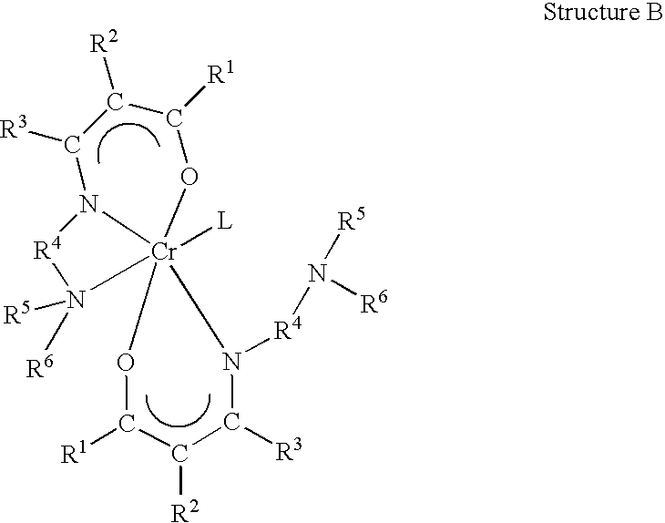
According to yet another embodiment, a chromium containing complex of a polydentate β-ketoiminate is selected from the group consisting of structure A,
Figure US07919409-20110405-C00001
and structure B;
Figure US07919409-20110405-C00002

wherein: R1 is a branched bulky alkyl group containing 1 to 6 carbon atoms; R2 is selected from the group consisting of hydrogen, alkyl having from 1 to 6 carbon atoms, alkoxy having from 1 to 6 carbon atoms, cycloaliphatic having from 3 to 6 carbon atoms, and aryl having from 6 to 10 carbon atoms; R3-4 are linear or branched selected from the group consisting of alkyl having from 1 to 6 carbon atoms, alkoxy having from 1 to 6 carbon atoms, cycloaliphatic having from 3 to 6 carbon atoms, and aryl having from 6 to 10 carbon atoms; R5-6 are linear or branched, individually selected from the group consisting of linear alkyl having from 1 to 6 carbon atoms, fluoroalkyl having from 1 to 6 carbon atoms, cycloaliphatic having from 3 to 10 carbon atoms, aryl having from 6 to 10 carbon atoms, and heterocyclic containing either oxygen, or nitrogen atoms; L is monodentate donor ligand.
BRIEF DESCRIPTION OF SEVERAL VIEWS OF THE DRAWINGS
FIG. 1 Structure of tantalum-nitride TaN(111) surface: (a) side view; (b) top view.
FIG. 2 Snapshot of the MD trajectory.
FIG. 3 (a) Copper (Cu) monolayer on top of a ruthenium (Ru) monolayer commensurate to the TaN(111) substrate. (b) initial and equilibrium structures of a Cu monolayer on Ru slab.
FIG. 4 Cu monolayer on top of a tantalum (Ta) monolayer commensurate to the TaN(111) substrate.
FIG. 5 Cu monolayer on top of a chromium (Cr) monolayer commensurate to the TaN(111) substrate.
FIG. 6( a) The equilibrium structure of Chromium binary with Vanadium (CrV) adhesion promoting layer on TaN(111) surface with top view and side view. FIG. 6( b) The equilibrium structure of Cu monolayer on the CrV adhesion promoting layer on TaN(111) surface with top view and side view.
FIG. 7( a) The equilibrium structure of Chromium binary with Titanium (CrTi) adhesion promoting layer on TaN(111) surface with top view and side view. FIG. 7( b) The equilibrium structure of Cu monolayer on the CrTi adhesion promoting layer on TaN(111) surface with top view and side view.
FIG. 8( a) The equilibrium structure of Chromium binary with Zirconium (CrZr) adhesion promoting layer on TaN(111) surface with top view and side view. FIG. 8( b) The equilibrium structure of Cu monolayer on the CrZr adhesion promoting layer on TaN(111) surface with top view and side view.
FIG. 9( a) The equilibrium structure of Chromium binary with Niobium (CrNb) adhesion promoting layer on TaN(111) surface with top view and side view. FIG. 9( b) The equilibrium structure of Cu monolayer on the CrNb adhesion promoting layer on TaN(111) surface with top view and side view.
FIG. 10. Crystal structure of bis(2,2-dimethyl-5-(dimethylaminoethyl-imino)-3-hexanonato-N,O,N′)(hydroxyl)chromium.
DETAILED DESCRIPTION OF THE INVENTION
Copper adhesion to barrier layers and electromigration resistance are extremely important properties affecting device yield and device lifetimes.
In the present invention, the state-of-the-art computational chemistry techniques have been used to identify adhesion promoting layer materials that provide good adhesion of metal seed layer to the adhesion promoting layer and the adhesion promoting layer to the barrier layer.
In accordance with embodiments of the present invention, adhesion promoting layer, or a “glue” layer, is applied directly to a barrier layer to improve the adhesion of the subsequently deposited metal seed layer.
Suitable barrier layers comprise a material selected from the group consisting of: tantalum (Ta), tantalum-nitride (TaN), tantalum-silicon-nitride (TaSiN), titanium (Ti), titanium-nitride (TiN), and mixtures thereof.
Suitable metal seed layer is selected from a copper layer, a copper alloy layer, and combinations thereof.
Several adhesion promoting layer materials based on chromium alloys have been shown to be able to significantly enhance the adhesion of the copper seed layer. The adhesion promoting layer, or a “glue” layer, comprises a chromium alloy having a formulation of CrxMy, where M is a group 4 to 12 metal, such as, copper (Cu), silver (Ag), ruthenium (Ru), vanadium (V), tantalum (Ta), titanium (Ti), zirconium (Zr) and niobium (Nb), x is the atomic weight percentage of Cr, y is the atomic weight percentage of M, and x+y=100%.
Suitable chromium alloys including chromium and about 10% to about 90% atomic weight percentage of an alloying element. As examples, the chromium alloys include chromium-copper (CrxCuy), chromium-silver (CrxAgy), chromium-ruthenium (CrxRuy), chromium-vanadium (CrxVy), chromium-tantalum (CrxTay), chromium-titanium (CrxTiy), chromium-zirconium (CrxZry) and chromium-niobium (CrxNby); where x is in the range of 10% to 90%.
Suitable chromium containing precursors for depositing the chromium alloys are chromium containing complexes of a polydentate β-ketoiminate represented by the following structures A and B:
Figure US07919409-20110405-C00003

wherein: R1 is a branched bulky alkyl group containing 1 to 6 carbon atoms; R2 is selected from the group consisting of hydrogen, alkyl having from 1 to 6 carbon atoms, alkoxy having from 1 to 6 carbon atoms, cycloaliphatic having from 3 to 6 carbon atoms, and aryl having from 6 to 10 carbon atoms; R3-4 are linear or branched selected from the group consisting of alkyl having from 1 to 6 carbon atoms, alkoxy having from 1 to 6 carbon atoms, cycloaliphatic having from 3 to 6 carbon atoms, and aryl having from 6 to 10 carbon atoms; R5-6 are linear or branched, individually selected from the group consisting of linear alkyl having from 1 to 6 carbon atoms, fluoroalkyl having from 1 to 6 carbon atoms, cycloaliphatic having from 3 to 10 carbon atoms, aryl having from 6 to 10 carbon atoms, and heterocyclic containing either oxygen, or nitrogen atoms; L is monodentate donor ligand.
Additional objects, advantages, and novel features of this invention will become apparent to those skilled in the art upon examination of the following embodiments thereof, which are not intended to be limiting.
EMBODIMENTS
The TaN(111) surface is described with a slab model containing four alternating layers with Ta (tantalum) and N (nitrogen) with N on top (FIG. 1). The selected unit cell contains 32 Ta and 32 N atoms and the surface cell parameters were fully optimized (a=12.416 Å, b=10.7533 Å, alpha=90°). In between slabs there is an approximately 24 Å vacuum space to prevent effective interaction between slabs. The bottom two layers are kept fixed and the top two layers as well as the Cu adatoms are fully relaxed.
Density functional theory (DFT) calculations under the generalized gradient approximation were performed using the exchange-correlation functional proposed by Perdew-Wang. The PAW pseudopotentials are used to represent the core electrons, while the valence orbitals are described by a plane wave basis set with 400 eV energy cut-off, which is sufficient to produce well-converged results. The electronically open-shell system was treated with a spin polarization scheme. The Brillouin zone integration was performed using the Monkhorst and Pack scheme with 2×2×1 k-points. Calculations with higher k-points (4×4×2) were also performed for dimer formation on the TaN(111) surface and the results were found to be virtually identical to those obtained with 2×2×1 k-points.
All structures were first optimized using the conjugate gradient algorithm and the computational accuracy was tested by calculating the cohesive energy of bulk copper. The calculated cohesive energy is 0.05 eV higher than the experimental value of 3.49 eV, suggesting that the method used in the present study is very accurate.
We subsequently performed ab initio molecular dynamics (MD) simulations for duration of 3.5 ps with a time step of 1 fs at 500 K to study the dynamic behavior of a Cu monolayer on the barrier surface in a canonical ensemble using the Nose thermostat for temperature control. All calculations were carried out using the VASP simulation package.
Ab initio molecular dynamics simulation (MD) was performed on the fully equilibrated TaN(111) surface with a Cu monolayer at 500° K, which is in a typical ALD temperature range.
FIG. 2 displays several selected snapshots of the MD trajectory.
Initially, the Cu monolayer is well aligned and commensurate with the substrate. Cu atoms are then quickly disassembled and move away from their equilibrium positions through surface diffusion upon MD run. At t=1 ps, some of the Cu atoms start moving upward to grow 3-dimensionally. At t=3 ps, the Cu atoms are aggregated together, forming surface islands, and the perfectly ordered monolayer structure becomes significantly disordered. Further MD runs prompt Cu atoms to move continuously, forming surface islands of various shapes, but no wetting of copper clusters on the surface was observed.
The calculated adhesion energy of Cu monolayer on TaN(111) is 2.65 eV.
First Embodiment Ru (Ruthenium) as an Adhesion Promoting Material
Ab initio molecular dynamics simulation was performed on the fully equilibrated surface with a Cu monolayer on top of a monolayer of Ru commensurate with TaN(111) surface at 500° K.
FIG. 3 a displays a fully equilibrated structure upon 4 ps MD simulation. No agglomeration of Cu atoms, other than simple thermal motion, was observed. Placing the same monolayer on several layers of Ru, as shown in FIG. 3 b, results in no agglomeration of Cu atoms.
The calculated adhesion energy of Cu monolayer on the Ru monolayer is 3.50 eV and the calculated adhesion energy of Ru monolayer on TaN(111) is 5.01 eV, significantly larger than the adhesion energy of Cu monolayer on TaN(111). The results suggest that Cu monolayer will not agglomerate on the Ru adhesion promoting layer.
Second Embodiment Ta (Tantalum) as an Adhesion Promoting Material
Ab initio molecular dynamics simulation was performed on the fully equilibrated surface with a Cu monolayer on top of a monolayer of Ta commensurate with TaN(111) surface at 500° K.
FIG. 4 displays a fully equilibrated structure upon 4 ps MD simulation. No agglomeration of Cu atoms, other than simple thermal motion, was observed. Placing the same monolayer on multi-layers of Ta results in no agglomeration of Cu atoms.
The calculated adhesion energy of Cu monolayer on the Ta monolayer is 3.84 eV and the calculated adhesion energy of Ta monolayer on TaN(111) is 7.72 eV, significantly larger than the adhesion energy of Cu monolayer on TaN(111). The results suggest that Cu monolayer will not agglomerate on the Ta adhesion promoting layer.
Third Embodiment Cr (Chromium) as an Adhesion Promoting Material
Ab initio molecular dynamics simulation was performed on the fully equilibrated surface with a Cu monolayer on top of a monolayer of Cr commensurate with TaN(111) surface at 500° K.
FIG. 5 displays a fully equilibrated structure upon 4 ps MD simulation. No agglomeration of Cu atoms, other than simple thermal motion, was observed. Placing the same monolayer on multi-layers of Cr results in no agglomeration of Cu atoms. The calculated adhesion energy of Cu monolayer on the Cr monolayer is 3.52 eV and the calculated adhesion energy of Ta monolayer on TaN(111) is 5.10 eV, significantly larger than the adhesion energy of Cu monolayer on TaN(111). The results suggest that Cu monolayer will not agglomerate on the Cr adhesion promoting layer.
Fourth Embodiment Cr (Chromium) Binary With V (Vanadium) as an Adhesion Promoting Material
Ab initio molecular dynamics simulation was performed on the fully equilibrated surface with a Cu monolayer on top of a monolayer of CrxVy alloy with x:y=1:1 commensurate with TaN(111) surface at 500° K.
FIG. 6 displays equilibrated structures upon 4 ps MD simulation. FIG. 6( a) displays a fully equilibrium structure of CrV adhesion promoting layer on TaN(111) surface with top view and side view. FIG. 6( b) displays a fully equilibrium structure of Cu monolayer on the CrV adhesion promoting layer on TaN(111) surface with top view and side view.
No agglomeration of Cu atoms, other than simple thermal motion, was observed. The calculated adhesion energy of Cu monolayer on the CrV alloy monolayer is 3.65 eV and the calculated adhesion energy of CrV monolayer on TaN(111) is 5.03 eV, significantly larger than the adhesion energy of Cu monolayer on TaN(111). The results suggest that Cu monolayer will not agglomerate on the CrV adhesion promoting layer.
Fifth Embodiment Cr (Chromium) Binary With Ti (Titanium) as an Adhesion Promoting Material
Ab initio molecular dynamics simulation was performed on the fully equilibrated surface with a Cu monolayer on top of a monolayer of CrxTiy alloy with x:y=1:1 commensurate with TaN(111) surface at 500° K.
FIG. 7 displays equilibrated structures upon 4 ps MD simulation. FIG. 7( a) displays the equilibrium structure of CrTi adhesion promoting layer on TaN(111) surface with top view and side view. FIG. 7( b) displays the equilibrium structure of Cu monolayer on the CrTi adhesion promoting layer on TaN(111) surface with top view and side view.
No agglomeration of Cu atoms, other than simple thermal motion, was observed. The calculated adhesion energy of Cu monolayer on the CrTi alloy monolayer is 3.67 eV and the calculated adhesion energy of CrTi monolayer on TaN(111) is 5.51 eV, significantly larger than the adhesion energy of Cu monolayer on TaN(111). The results suggest that Cu monolayer will not agglomerate on the CrTi adhesion promoting layer.
Sixth Embodiment Cr (Chromium) Binary With Zr (Zirconium) as an Adhesion Promoting Material
Ab initio molecular dynamics simulation was performed on the fully equilibrated surface with a Cu monolayer on top of a monolayer of CrxZry alloy with x:y=1:1 commensurate with TaN(111) surface at 500° K.
FIG. 8 displays equilibrated structures upon 4 ps MD simulation. FIG. 8( a) displays the equilibrium structure of CrZr adhesion promoting layer on TaN(111) surface with top view and side view. FIG. 8( b) displays the equilibrium structure of Cu monolayer on the CrZr adhesion promoting layer on TaN(111) surface with top view and side view.
No agglomeration of Cu atoms, other than simple thermal motion, was observed. The calculated adhesion energy of Cu monolayer on the CrZr alloy monolayer is 3.75 eV and the calculated adhesion energy of CrZr monolayer on TaN(111) is 6.09 eV, significantly larger than the adhesion energy of Cu monolayer on TaN(111). The results suggest that Cu monolayer will not agglomerate on the CrZr adhesion promoting layer.
Seventh Embodiment Cr (Chromium) Binary With Nb (Niobium) as an Adhesion Promoting Material
Ab initio molecular dynamics simulation was performed on the fully equilibrated surface with a Cu monolayer on top of a monolayer of CrxNby alloy with x:y=1:1 commensurate with TaN(111) surface at 500° K.
FIG. 9 displays equilibrated structures upon 4 ps MD simulation. FIG. 9( a) displays the equilibrium structure of CrNb adhesion promoting layer on TaN(111) surface with top view and side view. FIG. 9( b) displays the equilibrium structure of Cu monolayer on the CrNb adhesion promoting layer on TaN(111) surface with top view and side view.
No agglomeration of Cu atoms, other than simple thermal motion, was observed. The calculated adhesion energy of Cu monolayer on the CrNb alloy monolayer is 3.77 eV and the calculated adhesion energy of CrNb monolayer on TaN(111) is 5.64 eV, significantly larger than the adhesion energy of Cu monolayer on TaN(111). The results suggest that Cu monolayer will not agglomerate on the CrNb adhesion promoting.
Working Example Cr (Chromium) Containing Precursor Synthesis of bis(2,2-dimethyl-5-(dimethylaminoethyl-imino)-3-hexanonato-N,O,N′)(hydroxyl)chromium
To a slushy solution of 3.45 (16.27 mmol) ligand C in 25 mL hexanes at −40° C. was added 6.51 mL (16.27 mmol) 2.5M n-BuLi in hexanes drop wise. Warmed yellow-green solution to room temperature and left to stir for 30 minutes. Evaporated off hexanes under vacuum and residual was taken up in 25 mL THF. This solution was added to a suspension of 1.00 g (8.14 mmol) CrCl2 in 10 mL THF at room temperature via canula. Heated to 60° C. for 16 hours. Evaporated off volatiles under vacuum to a dark brown oil that was taken up in hot hexanes and filtered. Isolated 2.12 g of crude product that was sublimed at 100° C. under 90 mTorr vacuum over a period of 16 hours. Needle-like crystals were grown from pentane from sublimed material. 55% crude yield.
Crystal structure of bis(2,2-dimethyl-5-(dimethylaminoethyl-imino)-3-hexanonato-N,O,N′)(hydroxyl)chromium is shown in FIG. 10.
In summary, several adhesion promoting layer materials based on chromium alloys have been identified to be able to significantly enhance the adhesion of copper films. Table I summarizes the adhesion energy between the barrier layer TaN(111) and the adhesion promoting layer (ΔEAB), and the adhesion energy between the copper seed layer and the adhesion promoting layer (ΔECuA) (unit: eV).
TABLE 1
The calculated Adhesion Energy (eV)
TaN (111) Cu Ru Ta Cr CrTi CrNb CrZr
ΔEAB 2.65 5.01 7.72 5.10 5.51 5.64 6.09
ΔECuA 3.50 3.84 3.52 3.67 3.77 3.75
We have identified factors responsible for providing good adhesion of copper layer on various metallic surfaces and circumstances under which agglomeration of copper film occur.
To stabilize the adhesion promoting layer and prevent the agglomeration, the adhesion energy of the adhesion promoting layer on the barrier layer should be higher than the adhesion energy of copper on the barrier layer.
To stabilize the copper film and prevent the agglomeration, the adhesion energy of the copper seed layer on the adhesion promoting layer should be higher than the adhesion energy of copper on the barrier layer (otherwise, the copper seed layer would agglomerate on the glue layer);
To prevent diffusion of adhesion promoting layer atoms into the copper layer, the adhesion energy of adhesion promoting layer on the barrier layer should be higher than the adhesion energy of the copper seed layer on the glue layer.
Chromium containing complexes of a polydentate β-ketoiminate have been identified as chromium containing precursors to make the chromium alloys used for the adhesion promoting layer.
The embodiments of this invention listed above, including the working example, are exemplary of numerous embodiments that may be made of this invention. It is contemplated that numerous other configurations of the process may be used, and the materials used in the process may be elected from numerous materials other than those specifically disclosed.

Claims (11)

1. A method for controlling agglomeration and improving adhesion of a semiconductor device comprising:
a. providing a substrate comprising at least one patterned dielectric layer and at least one barrier layer;
b. depositing an adhesion promoting layer comprising a chromium alloy on the at least one barrier layer; and
c. depositing a metal seed layer on the adhesion promoting layer;
wherein adhesion energy between the adhesion promoting layer and the barrier layer is higher than adhesion energy between the adhesion promoting layer and the metal seed layer;
wherein the chromium alloy is deposited from a chromium containing precursor having complexes of a polydentate β-ketoiminate selected from the group consisting of structure A,
Figure US07919409-20110405-C00004
and structure B;
Figure US07919409-20110405-C00005
wherein: R1 is a branched bulky alkyl group containing 1 to 6 carbon atoms; R2 is selected from the group consisting of hydrogen, alkyl having from 1 to 6 carbon atoms, alkoxy having from 1 to 6 carbon atoms, cycloaliphatic having from 3 to 6 carbon atoms, and aryl having from 6 to 10 carbon atoms; R3-4 are linear or branched selected from the group consisting of alkyl having from 1 to 6 carbon atoms, alkoxy having from 1 to 6 carbon atoms, cycloaliphatic having from 3 to 6 carbon atoms, and aryl having from 6 to 10 carbon atoms; R5-6 are linear or branched, individually selected from the group consisting of linear alkyl having from 1 to 6 carbon atoms, fluoroalkyl having from 1 to 6 carbon atoms, cycloaliphatic having from 3 to 10 carbon atoms, aryl having from 6 to 10 carbon atoms, and heterocyclic containing either oxygen, or nitrogen atoms; L is monodentate donor ligand.
2. The method in claim 1, wherein the chromium alloy having a formulation of CrxMy, wherein M is a metal selected from the group consisting of copper (Cu), silver (Ag), ruthenium (Ru), vanadium (V), tantalum (Ta), titanium (Ti), zirconium (Zr) and niobium (Nb), x is the atomic weight percentage of Cr, y is the atomic weight percentage of M, and x+y=100%.
3. The method in claim 2, wherein the chromium alloy is selected from the group consisting of chromium-copper (CrxCuy), chromium-silver (CrxAgy), chromium-ruthenium (CrxRuy), chromium-vanadium (CrxVy), chromium-tantalum (CrxTay), chromium-titanium (CrxTiy), chromium-zirconium (CrxZry) and chromium-niobium (CrxNby); wherein x is in the range of 10% to 90%.
4. The method in claim 1, wherein the barrier layer comprises a material selected from the group consisting of: tantalum (Ta), tantalum-nitride (TaN), tantalum-silicon-nitride (TaSiN), titanium (Ti), titanium-nitride (TiN), and mixtures thereof.
5. The method in claim 1, wherein the metal seed layer is selected from the group consisting of a copper layer, a copper alloy layer, and combinations there of.
6. The method in claim 1, wherein the adhesion promoting layer is deposed by a process selected from the group consisting of Atomic Layer Deposition (ALD), Plasma Enhanced Atomic Layer Deposition (PEALD), Chemical Vapor Deposition (CVD), and Plasma Enhanced Chemical Vapor Deposition (PECVD), Low Pressure Chemical Vapor Deposition (LPCVD), Sub Atmospheric Chemical Vapor Deposition (SACVD), UV assisted Chemical Vapor Deposition, Filament assisted Chemical Vapor Deposition (FACVD), and Atmospheric Pressure Chemical Vapor Deposition (APCVD).
7. A method for controlling agglomeration of a copper layer and improving adhesion between a copper layer and at least one barrier layer comprising:
(1) providing a substrate comprising the at least one barrier layer on the top of at least one patterned dielectric layer;
(2) depositing an adhesion promoting layer comprising a chromium alloy on the at least one barrier layer, and
(3) depositing the copper layer on the adhesion promoting layer;
wherein adhesion energy between the adhesion promoting layer and the barrier layer is higher than adhesion energy between the adhesion promoting layer and the copper layer;
wherein the chromium alloy is deposited from a chromium containing precursor having complexes of a polydentate β-ketoiminate selected from the group consisting of structure A,
Figure US07919409-20110405-C00006
and structure B;
Figure US07919409-20110405-C00007
wherein: R1 is a branched bulky alkyl group containing 1 to 6 carbon atoms; R2 is selected from the croup consisting of hydrogen, alkyl having from 1 to 6 carbon atoms, alkoxy having from 1 to 6 carbon atoms, cycloaliphatic having from 3 to 6 carbon atoms, and aryl having from 6 to 10 carbon atoms; R3-4 are linear or branched selected from the group consisting of alkyl having from 1 to 6 carbon atoms, alkoxy having from 1 to 6 carbon atoms, cycloaliphatic having from 3 to 6 carbon atoms, and aryl having from 6 to 10 carbon atoms; R5-6 are linear or branched, individually selected from the group consisting of linear alkyl having from 1 to 6 carbon atoms, fluoroalkyl having from 1 to 6 carbon atoms, cycloaliphatic having from 3 to 10 carbon atoms, aryl having from 6 to 10 carbon atoms, and heterocyclic containing either oxygen, or nitrogen atoms; L is monodentate donor ligand.
8. The method in claim 7, wherein the chromium alloy having a formulation of CrxMy, where M is a metal selected from the group consisting of copper (Cu), silver (Ag), ruthenium (Ru), vanadium (V), tantalum (Ta), titanium (Ti), zirconium (Zr) and niobium (Nb), x is the atomic weight percentage of Cr, y is the atomic weight percentage of M, and x+y=100%.
9. The method in claim 8, wherein the chromium alloy is selected from the group consisting of chromium-copper (CrxCuy), chromium-silver (CrxAgy), chromium-ruthenium (CrxRuy), chromium-vanadium (CrxVy), chromium-titanium (CrxTay), chromium-zirconium (CrxZry) and chromium-niobium (CrxNby); wherein x is in the range of 10% to 90%.
10. The method in claim 7, wherein the barrier layer comprises a material selected from the group consisting of: tantalum (Ta), tantalum-nitride (TaN), tantalum-silicon-nitride (TaSiN), titanium (Ti), titanium-nitride (TiN), and mixtures thereof.
11. The method in claim 7, wherein the adhesion layer is deposed by a process selected from the group consisting of Atomic Layer Deposition (ALD), Plasma Enhanced Atomic Layer Deposition (PEALD), Chemical Vapor Deposition (CVD), and Plasma Enhanced Chemical Vapor Deposition (PECVD), Low Pressure Chemical Vapor Deposition (LPCVD), Sub Atmospheric Chemical Vapor Deposition (SACVD), UV-assisted Chemical Vapor Deposition, Filament-assisted Chemical Vapor Deposition (FACVD), and Atmospheric Pressure Chemical Vapor Deposition (APCVD).
US12/192,603 2008-08-15 2008-08-15 Materials for adhesion enhancement of copper film on diffusion barriers Expired - Fee Related US7919409B2 (en)

Priority Applications (6)

Application Number Priority Date Filing Date Title
US12/192,603 US7919409B2 (en) 2008-08-15 2008-08-15 Materials for adhesion enhancement of copper film on diffusion barriers
TW098127186A TW201007844A (en) 2008-08-15 2009-08-12 Materials for adhesion enhancement of copper film on diffusion barriers
JP2009188053A JP2010062555A (en) 2008-08-15 2009-08-14 Method for suppressing agglomeration and improving semiconductor device adhesiveness
EP09167949A EP2154717A2 (en) 2008-08-15 2009-08-14 Materials for adhesion enhancement of copper film on diffusion barriers
KR1020090075179A KR20100021379A (en) 2008-08-15 2009-08-14 Materials for adhesion enhancement of copper film on diffusion barriers
CN200910173396A CN101673706A (en) 2008-08-15 2009-08-14 Materials for adhesion enhancement of copper film on diffusion barriers

Applications Claiming Priority (1)

Application Number Priority Date Filing Date Title
US12/192,603 US7919409B2 (en) 2008-08-15 2008-08-15 Materials for adhesion enhancement of copper film on diffusion barriers

Publications (2)

Publication Number Publication Date
US20100038785A1 US20100038785A1 (en) 2010-02-18
US7919409B2 true US7919409B2 (en) 2011-04-05

Family

ID=41319973

Family Applications (1)

Application Number Title Priority Date Filing Date
US12/192,603 Expired - Fee Related US7919409B2 (en) 2008-08-15 2008-08-15 Materials for adhesion enhancement of copper film on diffusion barriers

Country Status (6)

Country Link
US (1) US7919409B2 (en)
EP (1) EP2154717A2 (en)
JP (1) JP2010062555A (en)
KR (1) KR20100021379A (en)
CN (1) CN101673706A (en)
TW (1) TW201007844A (en)

Cited By (1)

* Cited by examiner, † Cited by third party
Publication number Priority date Publication date Assignee Title
US20090237209A1 (en) * 2008-03-20 2009-09-24 Brian William Seal Communicating keychain

Families Citing this family (3)

* Cited by examiner, † Cited by third party
Publication number Priority date Publication date Assignee Title
US8791018B2 (en) * 2006-12-19 2014-07-29 Spansion Llc Method of depositing copper using physical vapor deposition
KR100973277B1 (en) * 2008-08-29 2010-07-30 주식회사 하이닉스반도체 Metal wiring of semiconductor device and method for forming the same
EP3876307A4 (en) * 2018-11-09 2022-10-26 Shenzhen Yuanzi Technology Co., Ltd. Film and preparation process

Citations (28)

* Cited by examiner, † Cited by third party
Publication number Priority date Publication date Assignee Title
US5668054A (en) 1996-01-11 1997-09-16 United Microelectronics Corporation Process for fabricating tantalum nitride diffusion barrier for copper matallization
US5942799A (en) 1997-11-20 1999-08-24 Novellus Systems, Inc. Multilayer diffusion barriers
US6140231A (en) 1999-02-12 2000-10-31 Taiwan Semiconductor Manufacturing Company Robust diffusion barrier for Cu metallization
US6153519A (en) 1997-03-31 2000-11-28 Motorola, Inc. Method of forming a barrier layer
US6194310B1 (en) 2000-06-01 2001-02-27 Sharp Laboratories Of America, Inc. Method of forming amorphous conducting diffusion barriers
WO2001029893A1 (en) 1999-10-15 2001-04-26 Asm America, Inc. Method for depositing nanolaminate thin films on sensitive surfaces
US6271131B1 (en) 1998-08-26 2001-08-07 Micron Technology, Inc. Methods for forming rhodium-containing layers such as platinum-rhodium barrier layers
US6287965B1 (en) 1997-07-28 2001-09-11 Samsung Electronics Co, Ltd. Method of forming metal layer using atomic layer deposition and semiconductor device having the metal layer as barrier metal layer or upper or lower electrode of capacitor
US6331484B1 (en) 1999-03-29 2001-12-18 Lucent Technologies, Inc. Titanium-tantalum barrier layer film and method for forming the same
US20020045343A1 (en) 2000-05-15 2002-04-18 Mcelwee-White Lisa MOCVD of WNx thin films using imido precursors
US20030059980A1 (en) 2001-09-25 2003-03-27 Ling Chen Copper interconnect barrier layer structure and formation method
US6627542B1 (en) 1999-07-12 2003-09-30 Applied Materials, Inc. Continuous, non-agglomerated adhesion of a seed layer to a barrier layer
US20050051512A1 (en) 2000-06-05 2005-03-10 Taiwan Semiconductor Manufacturing Company, Ltd. Method of forming multilayer diffusion barrier for copper interconnections
US20050070097A1 (en) 2003-09-29 2005-03-31 International Business Machines Corporation Atomic laminates for diffusion barrier applications
US20050167837A1 (en) 2004-01-21 2005-08-04 International Business Machines Corporation Device with area array pads for test probing
US20050274621A1 (en) 2004-06-10 2005-12-15 Zhi-Wen Sun Method of barrier layer surface treatment to enable direct copper plating on barrier metal
KR20060001306A (en) 2004-06-30 2006-01-06 매그나칩 반도체 유한회사 Method of forming a diffusion barrier in a semiconductor device
US6989321B2 (en) 2003-09-30 2006-01-24 Tokyo Electron Limited Low-pressure deposition of metal layers from metal-carbonyl precursors
US7034169B1 (en) * 2004-12-30 2006-04-25 Air Products And Chemicals, Inc. Volatile metal β-ketoiminate complexes
FR2883287A1 (en) 2005-03-16 2006-09-22 Air Liquide Preparing organometallic precursor molecules comprises introducing reagents in reactor, reacting to obtain solid-liquid phase mixture, filtering to recover liquid phase and removing solvents present in liquid phase by distillation
WO2006115476A2 (en) 2005-04-21 2006-11-02 Honeywell International Inc. Ruthenium-based materials and ruthenium alloys
US7205422B2 (en) * 2004-12-30 2007-04-17 Air Products And Chemicals, Inc. Volatile metal β-ketoiminate and metal β-diiminate complexes
US7220671B2 (en) 2005-03-31 2007-05-22 Intel Corporation Organometallic precursors for the chemical phase deposition of metal films in interconnect applications
US7223695B2 (en) 2004-09-30 2007-05-29 Intel Corporation Methods to deposit metal alloy barrier layers
US20070123043A1 (en) 2005-11-30 2007-05-31 Christof Streck A semiconductor device comprising a copper alloy as a barrier layer in a copper metallization layer
US20070184578A1 (en) * 2006-02-07 2007-08-09 Yaojian Lin Solder bump confinement system for an integrated circuit package
US20070264816A1 (en) 2006-05-12 2007-11-15 Lavoie Adrien R Copper alloy layer for integrated circuit interconnects
US20100018439A1 (en) * 2008-07-22 2010-01-28 Advanced Technology Materials, Inc. Precursors for cvd/ald of metal-containing films

Family Cites Families (9)

* Cited by examiner, † Cited by third party
Publication number Priority date Publication date Assignee Title
SG70654A1 (en) * 1997-09-30 2000-02-22 Ibm Copper stud structure with refractory metal liner
US6539625B2 (en) * 2001-01-11 2003-04-01 International Business Machines Corporation Chromium adhesion layer for copper vias in low-k technology
JP2003298203A (en) * 2002-03-29 2003-10-17 Nippon Zeon Co Ltd Printed wiring board and manufacturing method thereof
JP4228270B2 (en) * 2002-07-02 2009-02-25 富士通株式会社 Method for forming conductor pattern and mounting circuit board
DE102005004660A1 (en) 2004-07-02 2006-02-02 C. Rob. Hammerstein Gmbh & Co. Kg Motor vehicle seat with a Längsverstellvorrichtung with a seat support and rear wings
JP4322189B2 (en) * 2004-09-02 2009-08-26 株式会社ルネサステクノロジ Semiconductor device
JP2007103834A (en) * 2005-10-07 2007-04-19 Taiyo Yuden Co Ltd Semiconductor device and method for manufacturing the same
US7947814B2 (en) * 2006-04-25 2011-05-24 Air Products And Chemicals, Inc. Metal complexes of polydentate beta-ketoiminates
KR101150124B1 (en) * 2009-03-11 2012-06-08 에어 프로덕츠 앤드 케미칼스, 인코오포레이티드 Method for preparing metal complexes of polydentate beta-ketoiminates

Patent Citations (28)

* Cited by examiner, † Cited by third party
Publication number Priority date Publication date Assignee Title
US5668054A (en) 1996-01-11 1997-09-16 United Microelectronics Corporation Process for fabricating tantalum nitride diffusion barrier for copper matallization
US6153519A (en) 1997-03-31 2000-11-28 Motorola, Inc. Method of forming a barrier layer
US6287965B1 (en) 1997-07-28 2001-09-11 Samsung Electronics Co, Ltd. Method of forming metal layer using atomic layer deposition and semiconductor device having the metal layer as barrier metal layer or upper or lower electrode of capacitor
US5942799A (en) 1997-11-20 1999-08-24 Novellus Systems, Inc. Multilayer diffusion barriers
US6271131B1 (en) 1998-08-26 2001-08-07 Micron Technology, Inc. Methods for forming rhodium-containing layers such as platinum-rhodium barrier layers
US6140231A (en) 1999-02-12 2000-10-31 Taiwan Semiconductor Manufacturing Company Robust diffusion barrier for Cu metallization
US6331484B1 (en) 1999-03-29 2001-12-18 Lucent Technologies, Inc. Titanium-tantalum barrier layer film and method for forming the same
US6627542B1 (en) 1999-07-12 2003-09-30 Applied Materials, Inc. Continuous, non-agglomerated adhesion of a seed layer to a barrier layer
WO2001029893A1 (en) 1999-10-15 2001-04-26 Asm America, Inc. Method for depositing nanolaminate thin films on sensitive surfaces
US20020045343A1 (en) 2000-05-15 2002-04-18 Mcelwee-White Lisa MOCVD of WNx thin films using imido precursors
US6194310B1 (en) 2000-06-01 2001-02-27 Sharp Laboratories Of America, Inc. Method of forming amorphous conducting diffusion barriers
US20050051512A1 (en) 2000-06-05 2005-03-10 Taiwan Semiconductor Manufacturing Company, Ltd. Method of forming multilayer diffusion barrier for copper interconnections
US20030059980A1 (en) 2001-09-25 2003-03-27 Ling Chen Copper interconnect barrier layer structure and formation method
US20050070097A1 (en) 2003-09-29 2005-03-31 International Business Machines Corporation Atomic laminates for diffusion barrier applications
US6989321B2 (en) 2003-09-30 2006-01-24 Tokyo Electron Limited Low-pressure deposition of metal layers from metal-carbonyl precursors
US20050167837A1 (en) 2004-01-21 2005-08-04 International Business Machines Corporation Device with area array pads for test probing
US20050274621A1 (en) 2004-06-10 2005-12-15 Zhi-Wen Sun Method of barrier layer surface treatment to enable direct copper plating on barrier metal
KR20060001306A (en) 2004-06-30 2006-01-06 매그나칩 반도체 유한회사 Method of forming a diffusion barrier in a semiconductor device
US7223695B2 (en) 2004-09-30 2007-05-29 Intel Corporation Methods to deposit metal alloy barrier layers
US7034169B1 (en) * 2004-12-30 2006-04-25 Air Products And Chemicals, Inc. Volatile metal β-ketoiminate complexes
US7205422B2 (en) * 2004-12-30 2007-04-17 Air Products And Chemicals, Inc. Volatile metal β-ketoiminate and metal β-diiminate complexes
FR2883287A1 (en) 2005-03-16 2006-09-22 Air Liquide Preparing organometallic precursor molecules comprises introducing reagents in reactor, reacting to obtain solid-liquid phase mixture, filtering to recover liquid phase and removing solvents present in liquid phase by distillation
US7220671B2 (en) 2005-03-31 2007-05-22 Intel Corporation Organometallic precursors for the chemical phase deposition of metal films in interconnect applications
WO2006115476A2 (en) 2005-04-21 2006-11-02 Honeywell International Inc. Ruthenium-based materials and ruthenium alloys
US20070123043A1 (en) 2005-11-30 2007-05-31 Christof Streck A semiconductor device comprising a copper alloy as a barrier layer in a copper metallization layer
US20070184578A1 (en) * 2006-02-07 2007-08-09 Yaojian Lin Solder bump confinement system for an integrated circuit package
US20070264816A1 (en) 2006-05-12 2007-11-15 Lavoie Adrien R Copper alloy layer for integrated circuit interconnects
US20100018439A1 (en) * 2008-07-22 2010-01-28 Advanced Technology Materials, Inc. Precursors for cvd/ald of metal-containing films

Non-Patent Citations (11)

* Cited by examiner, † Cited by third party
Title
Alain E. Kaloyeros et al, Tantalum Nitride Films Grown by Inorganic Low Temperature Thermal Chemical Vapor Deposition, Journal of The Electrochemical Society, 1999, 170-176, 146(1).
F. Maury et al, Evaluation of tetra-alkylchromium precursors for organometallic chemical vapor deposition II. Unusual low temperature chromium carbide deposition from Cr[C(CH3)3]4, Thin Solid Films, 1992, 24-29, 219.
Francis Maury et al, Low-Temperature MOCVD of Chromium Carbonitride Coatings from Tetrakis (diethylamido) chromium and Pyrolysis Mechanism of this Single-Source Precursor, Applied Organometallic Chemistry, 1998, 189-199, 12.
Franco Ossola et al, MOCVD Route to Chromium Carbonitride Thin Films Using Cr(NEt2)4 as Single-Source Precursor: Growth and Mechanism, Chemical Vapor Deposition, 1997, 137-143, 3.
Jean E. Kelsey et al, Low Temperature metal-organic chemical vapor deposition of tungsten nitride as diffusion barrier for copper metallization, J. Vac. Sci. Technol., 1999, 1101-1104, 17(3).
Junghun Chae et al, Atomic Layer Deposition of Nickel by the Reduction of Preformed Nickel Oxide, Electrochemical and Solid-State Letters, 2002, C64-C66, 5(6).
Petra Alen et al, Atomic Layer Deposition of Molybdenum Nitride Thin Films for Cu Metallizations, Journal of The Electrochemical Society, 2005, G361-G366, 152(5).
Renaud Fix et al, Chemical Vapor Deposition of Vanadium, Niobium, and Tantalum Nitride Thin Films, Chem. Mater., 1993, 614-619, 5.
Soo-Hyun Kim et al, A Comparative Study of Film Properties of Chemical Vapor Deposited TiN Films as Diffusion Barriers for Cu Metallization, Journal of The Electrochemical Society, 1999, 1455-1460, 146(4).
Ville Miikkulainen et al, Atomic Layer Deposition of Molybdenum Nitride from Bis(tert-butylimido)-bis (dimethylamido)molybdenum and Ammonia onto Several Types of Substrate Materials with Equal Growth per Cycle, Chem. Mater., 2007, 263-269, 19.
Zhengwen Li et al, Nucleation and Adhesion of ALD Copper on Cobalt Adhesion Layers and Tungsten Nitride Diffusion Barriers, Electrochemical and Solid-State Letters, 2005, G182-G185, 8(7).

Cited By (1)

* Cited by examiner, † Cited by third party
Publication number Priority date Publication date Assignee Title
US20090237209A1 (en) * 2008-03-20 2009-09-24 Brian William Seal Communicating keychain

Also Published As

Publication number Publication date
EP2154717A2 (en) 2010-02-17
US20100038785A1 (en) 2010-02-18
JP2010062555A (en) 2010-03-18
TW201007844A (en) 2010-02-16
CN101673706A (en) 2010-03-17
KR20100021379A (en) 2010-02-24

Similar Documents

Publication Publication Date Title
Chang et al. Structural and thermodynamic factors of suppressed interdiffusion kinetics in multi-component high-entropy materials
KR101067364B1 (en) Conductive film forming method, thin film transistor, panel with thin film transistor and thin film transistor manufacturing method
US7919409B2 (en) Materials for adhesion enhancement of copper film on diffusion barriers
TW200827462A (en) Method for forming an electroconductive film, thin film transistor, panel having a thin film transistor and method for producing a thin film transistor
Bhandari et al. Chemical vapor deposition of cobalt nitride and its application as an adhesion-enhancing layer for advanced copper interconnects
US6337148B1 (en) Copper source reagent compositions, and method of making and using same for microelectronic device structures
Chen et al. Interdiffusion reliability and resistivity scaling of intermetallic compounds as advanced interconnect materials
TW440937B (en) Iridium conductive electrode/barrier structure and method for same
O'Nei et al. Reactive deposition of conformal ruthenium films from supercritical carbon dioxide
Wong et al. Prospective development in diffusion barrier layers for copper metallization in LSI
US20070281457A1 (en) Copper layer and a method for manufacturing said copper layer
US20080164580A1 (en) Chemical vapor deposition method for the incorporation of nitrogen into materials including germanium and antimony
Väyrynen et al. Nickel germanide thin films by atomic layer deposition
Shin et al. Growth of ultrathin films of amorphous ruthenium− phosphorus alloys using a single source CVD precursor
JP2008124450A (en) Target, film forming method, thin film transistor, panel with thin film transistor, manufacturing method for thin film transistor, and manufacturing method for panel with thin film transistor
Bhaskaran et al. Low-Pressure Chemical Vapor Deposition of Cu− Pd Films: Alloy Growth Kinetics
Valet et al. Study of platinum thin films deposited by MOCVD as electrodes for oxide applications
Choi et al. Effect of the neutral ligand (L) on the characteristics of hexafluoroacetylacetonate (hfac) Cu (I)-L precursor and on the copper deposition process
EP0650201B1 (en) Ohmic electrode for N-type semiconductor cubic boron nitride and method of producing same
Tsai et al. Diffusion barrier performance of TiVCr alloy film in Cu metallization
Song et al. The self-formation graded diffusion barrier of Zr/ZrN
Shin et al. Chemical routes to ultra thin films for copper barriers and liners
Zhong et al. Preliminary growth of metallic co films by thermal atomic layer deposition using RCpCo (CO) 2 and alkylamine precursors
US10793947B2 (en) Alloys of Co to reduce stress
US7834206B2 (en) Organic-metal precursor material and method of manufacturing metal thin film using the same

Legal Events

Date Code Title Description
AS Assignment

Owner name: AIR PRODUCTS AND CHEMICALS, INC.,PENNSYLVANIA

Free format text: ASSIGNMENT OF ASSIGNORS INTEREST;ASSIGNORS:CHENG, HANSONG;LEI, XINJIAN;SPENCE, DANIEL P.;AND OTHERS;SIGNING DATES FROM 20080903 TO 20080919;REEL/FRAME:021783/0559

Owner name: AIR PRODUCTS AND CHEMICALS, INC., PENNSYLVANIA

Free format text: ASSIGNMENT OF ASSIGNORS INTEREST;ASSIGNORS:CHENG, HANSONG;LEI, XINJIAN;SPENCE, DANIEL P.;AND OTHERS;SIGNING DATES FROM 20080903 TO 20080919;REEL/FRAME:021783/0559

CC Certificate of correction
REMI Maintenance fee reminder mailed
LAPS Lapse for failure to pay maintenance fees
STCH Information on status: patent discontinuation

Free format text: PATENT EXPIRED DUE TO NONPAYMENT OF MAINTENANCE FEES UNDER 37 CFR 1.362

FP Lapsed due to failure to pay maintenance fee

Effective date: 20150405

AS Assignment

Owner name: VERSUM MATERIALS US, LLC, ARIZONA

Free format text: ASSIGNMENT OF ASSIGNORS INTEREST;ASSIGNOR:AIR PRODUCTS AND CHEMICALS, INC.;REEL/FRAME:041772/0733

Effective date: 20170214