US7875408B2 - Bleachable materials for lithography - Google Patents
Bleachable materials for lithography Download PDFInfo
- Publication number
- US7875408B2 US7875408B2 US11/698,182 US69818207A US7875408B2 US 7875408 B2 US7875408 B2 US 7875408B2 US 69818207 A US69818207 A US 69818207A US 7875408 B2 US7875408 B2 US 7875408B2
- Authority
- US
- United States
- Prior art keywords
- aromatic
- combinations
- alicyclic
- light
- fluoroalkyl
- Prior art date
- Legal status (The legal status is an assumption and is not a legal conclusion. Google has not performed a legal analysis and makes no representation as to the accuracy of the status listed.)
- Expired - Fee Related, expires
Links
- 239000000463 material Substances 0.000 title claims abstract description 63
- 238000001459 lithography Methods 0.000 title description 4
- 229920000642 polymer Polymers 0.000 claims abstract description 73
- 238000000034 method Methods 0.000 claims abstract description 51
- 230000008569 process Effects 0.000 claims abstract description 39
- 239000000203 mixture Substances 0.000 claims abstract description 33
- 229920002120 photoresistant polymer Polymers 0.000 claims abstract description 30
- 238000004519 manufacturing process Methods 0.000 claims abstract description 23
- PPBRXRYQALVLMV-UHFFFAOYSA-N Styrene Chemical compound C=CC1=CC=CC=C1 PPBRXRYQALVLMV-UHFFFAOYSA-N 0.000 claims abstract description 22
- 125000000962 organic group Chemical group 0.000 claims abstract description 14
- 238000000206 photolithography Methods 0.000 claims abstract description 14
- 125000001424 substituent group Chemical group 0.000 claims abstract description 14
- 229920000058 polyacrylate Polymers 0.000 claims abstract description 9
- SLGWESQGEUXWJQ-UHFFFAOYSA-N formaldehyde;phenol Chemical compound O=C.OC1=CC=CC=C1 SLGWESQGEUXWJQ-UHFFFAOYSA-N 0.000 claims abstract description 7
- 125000004122 cyclic group Chemical group 0.000 claims abstract 5
- 150000001875 compounds Chemical class 0.000 claims description 52
- 125000003118 aryl group Chemical group 0.000 claims description 40
- 229910052799 carbon Inorganic materials 0.000 claims description 39
- 150000001923 cyclic compounds Chemical class 0.000 claims description 32
- 125000002723 alicyclic group Chemical group 0.000 claims description 28
- 125000003709 fluoroalkyl group Chemical group 0.000 claims description 27
- 229910052739 hydrogen Inorganic materials 0.000 claims description 27
- 239000001257 hydrogen Substances 0.000 claims description 27
- 125000003178 carboxy group Chemical group [H]OC(*)=O 0.000 claims description 20
- 150000002431 hydrogen Chemical class 0.000 claims description 20
- -1 phenolic acrylates Chemical class 0.000 claims description 20
- 125000005842 heteroatom Chemical group 0.000 claims description 19
- 125000002887 hydroxy group Chemical group [H]O* 0.000 claims description 17
- 125000002915 carbonyl group Chemical group [*:2]C([*:1])=O 0.000 claims description 16
- 125000003545 alkoxy group Chemical group 0.000 claims description 15
- 229910052736 halogen Inorganic materials 0.000 claims description 15
- 150000002367 halogens Chemical class 0.000 claims description 15
- 230000003287 optical effect Effects 0.000 claims description 14
- 229920000548 poly(silane) polymer Polymers 0.000 claims description 13
- 238000004061 bleaching Methods 0.000 claims description 11
- 239000000178 monomer Substances 0.000 claims description 10
- 230000008859 change Effects 0.000 claims description 9
- 238000010521 absorption reaction Methods 0.000 claims description 8
- 125000000217 alkyl group Chemical group 0.000 claims description 8
- 150000001728 carbonyl compounds Chemical class 0.000 claims description 8
- 239000006117 anti-reflective coating Substances 0.000 claims description 7
- 230000004888 barrier function Effects 0.000 claims description 7
- 239000004793 Polystyrene Substances 0.000 claims description 6
- 208000021668 chronic eosinophilic leukemia Diseases 0.000 claims description 6
- 125000004435 hydrogen atom Chemical group [H]* 0.000 claims description 6
- 229910052760 oxygen Inorganic materials 0.000 claims description 6
- 229920002223 polystyrene Polymers 0.000 claims description 6
- 229920001289 polyvinyl ether Polymers 0.000 claims description 6
- 239000002904 solvent Substances 0.000 claims description 6
- 239000004971 Cross linker Substances 0.000 claims description 5
- QVGXLLKOCUKJST-UHFFFAOYSA-N atomic oxygen Chemical compound [O] QVGXLLKOCUKJST-UHFFFAOYSA-N 0.000 claims description 5
- 125000004093 cyano group Chemical group *C#N 0.000 claims description 5
- 230000000694 effects Effects 0.000 claims description 5
- 125000000449 nitro group Chemical group [O-][N+](*)=O 0.000 claims description 5
- 229920003986 novolac Polymers 0.000 claims description 5
- 150000003961 organosilicon compounds Chemical class 0.000 claims description 5
- 239000001301 oxygen Substances 0.000 claims description 5
- 238000000671 immersion lithography Methods 0.000 claims description 4
- 239000004094 surface-active agent Substances 0.000 claims description 4
- UFHFLCQGNIYNRP-UHFFFAOYSA-N Hydrogen Chemical compound [H][H] UFHFLCQGNIYNRP-UHFFFAOYSA-N 0.000 claims description 2
- 125000001997 phenyl group Chemical group [H]C1=C([H])C([H])=C(*)C([H])=C1[H] 0.000 claims description 2
- 125000001544 thienyl group Chemical group 0.000 claims description 2
- 229920001795 coordination polymer Polymers 0.000 claims 8
- 230000001681 protective effect Effects 0.000 claims 6
- 239000007859 condensation product Substances 0.000 claims 4
- 239000002585 base Substances 0.000 claims 3
- 230000002708 enhancing effect Effects 0.000 claims 1
- 239000011368 organic material Substances 0.000 abstract description 13
- 230000002441 reversible effect Effects 0.000 abstract description 9
- 239000004065 semiconductor Substances 0.000 abstract description 8
- ISWSIDIOOBJBQZ-UHFFFAOYSA-N Phenol Chemical compound OC1=CC=CC=C1 ISWSIDIOOBJBQZ-UHFFFAOYSA-N 0.000 abstract description 7
- 229910052710 silicon Inorganic materials 0.000 abstract description 7
- 239000010703 silicon Substances 0.000 abstract description 7
- KJCVRFUGPWSIIH-UHFFFAOYSA-N 1-naphthol Chemical compound C1=CC=C2C(O)=CC=CC2=C1 KJCVRFUGPWSIIH-UHFFFAOYSA-N 0.000 abstract description 3
- 229920001568 phenolic resin Polymers 0.000 abstract description 3
- FLGPRDQFUUFZBL-UHFFFAOYSA-N formaldehyde;naphthalen-1-ol Chemical compound O=C.C1=CC=C2C(O)=CC=CC2=C1 FLGPRDQFUUFZBL-UHFFFAOYSA-N 0.000 abstract description 2
- 150000002894 organic compounds Chemical class 0.000 description 12
- 238000012545 processing Methods 0.000 description 12
- 230000005855 radiation Effects 0.000 description 10
- 239000000047 product Substances 0.000 description 8
- 238000006243 chemical reaction Methods 0.000 description 7
- 239000011159 matrix material Substances 0.000 description 7
- CSCPPACGZOOCGX-UHFFFAOYSA-N Acetone Chemical compound CC(C)=O CSCPPACGZOOCGX-UHFFFAOYSA-N 0.000 description 6
- UHOVQNZJYSORNB-UHFFFAOYSA-N Benzene Chemical compound C1=CC=CC=C1 UHOVQNZJYSORNB-UHFFFAOYSA-N 0.000 description 6
- WSFSSNUMVMOOMR-UHFFFAOYSA-N Formaldehyde Chemical compound O=C WSFSSNUMVMOOMR-UHFFFAOYSA-N 0.000 description 6
- OKKJLVBELUTLKV-UHFFFAOYSA-N Methanol Chemical compound OC OKKJLVBELUTLKV-UHFFFAOYSA-N 0.000 description 6
- YXFVVABEGXRONW-UHFFFAOYSA-N Toluene Chemical compound CC1=CC=CC=C1 YXFVVABEGXRONW-UHFFFAOYSA-N 0.000 description 6
- 239000002253 acid Substances 0.000 description 6
- 230000008901 benefit Effects 0.000 description 6
- 229920001577 copolymer Polymers 0.000 description 6
- VLKZOEOYAKHREP-UHFFFAOYSA-N n-Hexane Chemical class CCCCCC VLKZOEOYAKHREP-UHFFFAOYSA-N 0.000 description 6
- 125000002524 organometallic group Chemical group 0.000 description 6
- NIXOWILDQLNWCW-UHFFFAOYSA-M acrylate group Chemical group C(C=C)(=O)[O-] NIXOWILDQLNWCW-UHFFFAOYSA-M 0.000 description 5
- 239000000126 substance Substances 0.000 description 5
- 238000003786 synthesis reaction Methods 0.000 description 5
- RTZKZFJDLAIYFH-UHFFFAOYSA-N Diethyl ether Chemical compound CCOCC RTZKZFJDLAIYFH-UHFFFAOYSA-N 0.000 description 4
- XUIMIQQOPSSXEZ-UHFFFAOYSA-N Silicon Chemical compound [Si] XUIMIQQOPSSXEZ-UHFFFAOYSA-N 0.000 description 4
- WYURNTSHIVDZCO-UHFFFAOYSA-N Tetrahydrofuran Chemical compound C1CCOC1 WYURNTSHIVDZCO-UHFFFAOYSA-N 0.000 description 4
- 230000015572 biosynthetic process Effects 0.000 description 4
- 239000007844 bleaching agent Substances 0.000 description 4
- 230000005291 magnetic effect Effects 0.000 description 4
- 125000002496 methyl group Chemical group [H]C([H])([H])* 0.000 description 4
- GHMLBKRAJCXXBS-UHFFFAOYSA-N resorcinol Chemical compound OC1=CC=CC(O)=C1 GHMLBKRAJCXXBS-UHFFFAOYSA-N 0.000 description 4
- 239000000243 solution Substances 0.000 description 4
- 238000011282 treatment Methods 0.000 description 4
- MSKRHWFHKJMMJG-UHFFFAOYSA-N 1,3-di(anthracen-9-yl)propan-1-one Chemical compound C1=CC=C2C(C(CCC=3C4=CC=CC=C4C=C4C=CC=CC4=3)=O)=C(C=CC=C3)C3=CC2=C1 MSKRHWFHKJMMJG-UHFFFAOYSA-N 0.000 description 3
- NIXOWILDQLNWCW-UHFFFAOYSA-N 2-Propenoic acid Natural products OC(=O)C=C NIXOWILDQLNWCW-UHFFFAOYSA-N 0.000 description 3
- XEKOWRVHYACXOJ-UHFFFAOYSA-N Ethyl acetate Chemical compound CCOC(C)=O XEKOWRVHYACXOJ-UHFFFAOYSA-N 0.000 description 3
- 230000009102 absorption Effects 0.000 description 3
- 150000001299 aldehydes Chemical class 0.000 description 3
- 238000000576 coating method Methods 0.000 description 3
- 238000011161 development Methods 0.000 description 3
- 230000005684 electric field Effects 0.000 description 3
- 150000002576 ketones Chemical class 0.000 description 3
- 239000011541 reaction mixture Substances 0.000 description 3
- 239000007787 solid Substances 0.000 description 3
- 239000000758 substrate Substances 0.000 description 3
- 230000009466 transformation Effects 0.000 description 3
- 238000002834 transmittance Methods 0.000 description 3
- DPZNOMCNRMUKPS-UHFFFAOYSA-N 1,3-Dimethoxybenzene Chemical compound COC1=CC=CC(OC)=C1 DPZNOMCNRMUKPS-UHFFFAOYSA-N 0.000 description 2
- OHBQPCCCRFSCAX-UHFFFAOYSA-N 1,4-Dimethoxybenzene Chemical compound COC1=CC=C(OC)C=C1 OHBQPCCCRFSCAX-UHFFFAOYSA-N 0.000 description 2
- 239000004593 Epoxy Substances 0.000 description 2
- LFQSCWFLJHTTHZ-UHFFFAOYSA-N Ethanol Chemical compound CCO LFQSCWFLJHTTHZ-UHFFFAOYSA-N 0.000 description 2
- CSNNHWWHGAXBCP-UHFFFAOYSA-L Magnesium sulfate Chemical compound [Mg+2].[O-][S+2]([O-])([O-])[O-] CSNNHWWHGAXBCP-UHFFFAOYSA-L 0.000 description 2
- OFOBLEOULBTSOW-UHFFFAOYSA-N Malonic acid Chemical compound OC(=O)CC(O)=O OFOBLEOULBTSOW-UHFFFAOYSA-N 0.000 description 2
- VYPSYNLAJGMNEJ-UHFFFAOYSA-N Silicium dioxide Chemical compound O=[Si]=O VYPSYNLAJGMNEJ-UHFFFAOYSA-N 0.000 description 2
- QAOWNCQODCNURD-UHFFFAOYSA-N Sulfuric acid Chemical compound OS(O)(=O)=O QAOWNCQODCNURD-UHFFFAOYSA-N 0.000 description 2
- 239000000654 additive Substances 0.000 description 2
- MWPLVEDNUUSJAV-UHFFFAOYSA-N anthracene Chemical compound C1=CC=CC2=CC3=CC=CC=C3C=C21 MWPLVEDNUUSJAV-UHFFFAOYSA-N 0.000 description 2
- 238000013459 approach Methods 0.000 description 2
- PXKLMJQFEQBVLD-UHFFFAOYSA-N bisphenol F Chemical compound C1=CC(O)=CC=C1CC1=CC=C(O)C=C1 PXKLMJQFEQBVLD-UHFFFAOYSA-N 0.000 description 2
- 125000004432 carbon atom Chemical group C* 0.000 description 2
- 238000012668 chain scission Methods 0.000 description 2
- 125000000113 cyclohexyl group Chemical group [H]C1([H])C([H])([H])C([H])([H])C([H])(*)C([H])([H])C1([H])[H] 0.000 description 2
- 230000005672 electromagnetic field Effects 0.000 description 2
- 239000003822 epoxy resin Substances 0.000 description 2
- 150000002148 esters Chemical class 0.000 description 2
- 230000006870 function Effects 0.000 description 2
- 125000000524 functional group Chemical group 0.000 description 2
- 239000007789 gas Substances 0.000 description 2
- 229920001519 homopolymer Polymers 0.000 description 2
- 238000003384 imaging method Methods 0.000 description 2
- 229910052751 metal Inorganic materials 0.000 description 2
- 125000001570 methylene group Chemical group [H]C([H])([*:1])[*:2] 0.000 description 2
- 125000001280 n-hexyl group Chemical group C(CCCCC)* 0.000 description 2
- 150000004780 naphthols Chemical class 0.000 description 2
- 238000007539 photo-oxidation reaction Methods 0.000 description 2
- 238000007540 photo-reduction reaction Methods 0.000 description 2
- 238000006349 photocyclization reaction Methods 0.000 description 2
- 229920003229 poly(methyl methacrylate) Polymers 0.000 description 2
- 229920001515 polyalkylene glycol Polymers 0.000 description 2
- 229920000647 polyepoxide Polymers 0.000 description 2
- 239000004926 polymethyl methacrylate Substances 0.000 description 2
- 229920002451 polyvinyl alcohol Polymers 0.000 description 2
- 235000019422 polyvinyl alcohol Nutrition 0.000 description 2
- BWHMMNNQKKPAPP-UHFFFAOYSA-L potassium carbonate Chemical compound [K+].[K+].[O-]C([O-])=O BWHMMNNQKKPAPP-UHFFFAOYSA-L 0.000 description 2
- LLHKCFNBLRBOGN-UHFFFAOYSA-N propylene glycol methyl ether acetate Chemical compound COCC(C)OC(C)=O LLHKCFNBLRBOGN-UHFFFAOYSA-N 0.000 description 2
- 229920005989 resin Polymers 0.000 description 2
- 239000011347 resin Substances 0.000 description 2
- 239000000741 silica gel Substances 0.000 description 2
- 229910002027 silica gel Inorganic materials 0.000 description 2
- 238000000844 transformation Methods 0.000 description 2
- ABDKAPXRBAPSQN-UHFFFAOYSA-N veratrole Chemical compound COC1=CC=CC=C1OC ABDKAPXRBAPSQN-UHFFFAOYSA-N 0.000 description 2
- XLYOFNOQVPJJNP-UHFFFAOYSA-N water Substances O XLYOFNOQVPJJNP-UHFFFAOYSA-N 0.000 description 2
- YFSUTJLHUFNCNZ-UHFFFAOYSA-M 1,1,2,2,3,3,4,4,5,5,6,6,7,7,8,8,8-heptadecafluorooctane-1-sulfonate Chemical compound [O-]S(=O)(=O)C(F)(F)C(F)(F)C(F)(F)C(F)(F)C(F)(F)C(F)(F)C(F)(F)C(F)(F)F YFSUTJLHUFNCNZ-UHFFFAOYSA-M 0.000 description 1
- ZTUKGBOUHWYFGC-UHFFFAOYSA-N 1,3,3-trimethyl-2-methylideneindole Chemical compound C1=CC=C2N(C)C(=C)C(C)(C)C2=C1 ZTUKGBOUHWYFGC-UHFFFAOYSA-N 0.000 description 1
- UEFZEQYQHOCDKK-UHFFFAOYSA-N 1,3,5-trimethyl-2-[3-(2,4,6-trimethylphenyl)but-2-en-2-yl]benzene Chemical compound CC=1C=C(C)C=C(C)C=1C(C)=C(C)C1=C(C)C=C(C)C=C1C UEFZEQYQHOCDKK-UHFFFAOYSA-N 0.000 description 1
- YFKBXYGUSOXJGS-UHFFFAOYSA-N 1,3-Diphenyl-2-propanone Chemical compound C=1C=CC=CC=1CC(=O)CC1=CC=CC=C1 YFKBXYGUSOXJGS-UHFFFAOYSA-N 0.000 description 1
- VEAFKIYNHVBNIP-UHFFFAOYSA-N 1,3-Diphenylpropane Chemical compound C=1C=CC=CC=1CCCC1=CC=CC=C1 VEAFKIYNHVBNIP-UHFFFAOYSA-N 0.000 description 1
- ADLRERWVJNCCLW-UHFFFAOYSA-N 1,3-di(anthracen-9-yl)prop-2-en-1-one Chemical compound C1=CC=C2C(C(C=CC=3C4=CC=CC=C4C=C4C=CC=CC4=3)=O)=C(C=CC=C3)C3=CC2=C1 ADLRERWVJNCCLW-UHFFFAOYSA-N 0.000 description 1
- RYHBNJHYFVUHQT-UHFFFAOYSA-N 1,4-Dioxane Chemical compound C1COCCO1 RYHBNJHYFVUHQT-UHFFFAOYSA-N 0.000 description 1
- XWCIICLTKWRWCI-UHFFFAOYSA-N 1-(2,4,6-trimethylphenyl)ethanone Chemical compound CC(=O)C1=C(C)C=C(C)C=C1C XWCIICLTKWRWCI-UHFFFAOYSA-N 0.000 description 1
- NXXNVJDXUHMAHU-UHFFFAOYSA-N 1-anthracen-9-ylethanone Chemical compound C1=CC=C2C(C(=O)C)=C(C=CC=C3)C3=CC2=C1 NXXNVJDXUHMAHU-UHFFFAOYSA-N 0.000 description 1
- SMZOUWXMTYCWNB-UHFFFAOYSA-N 2-(2-methoxy-5-methylphenyl)ethanamine Chemical compound COC1=CC=C(C)C=C1CCN SMZOUWXMTYCWNB-UHFFFAOYSA-N 0.000 description 1
- HHDPXULKSZZACU-UHFFFAOYSA-N 2-hydroxy-4-nitrobenzaldehyde Chemical compound OC1=CC([N+]([O-])=O)=CC=C1C=O HHDPXULKSZZACU-UHFFFAOYSA-N 0.000 description 1
- MUZDXNQOSGWMJJ-UHFFFAOYSA-N 2-methylprop-2-enoic acid;prop-2-enoic acid Chemical compound OC(=O)C=C.CC(=C)C(O)=O MUZDXNQOSGWMJJ-UHFFFAOYSA-N 0.000 description 1
- KFZMGEQAYNKOFK-UHFFFAOYSA-N 2-propanol Substances CC(C)O KFZMGEQAYNKOFK-UHFFFAOYSA-N 0.000 description 1
- PBEHQFUSQJKBAS-UHFFFAOYSA-N 4-[2-(4-hydroxyphenyl)propan-2-yl]phenol;phenol Chemical compound OC1=CC=CC=C1.C=1C=C(O)C=CC=1C(C)(C)C1=CC=C(O)C=C1 PBEHQFUSQJKBAS-UHFFFAOYSA-N 0.000 description 1
- 240000000662 Anethum graveolens Species 0.000 description 1
- 238000005698 Diels-Alder reaction Methods 0.000 description 1
- BRLQWZUYTZBJKN-UHFFFAOYSA-N Epichlorohydrin Chemical compound ClCC1CO1 BRLQWZUYTZBJKN-UHFFFAOYSA-N 0.000 description 1
- CERQOIWHTDAKMF-UHFFFAOYSA-N Methacrylic acid Chemical compound CC(=C)C(O)=O CERQOIWHTDAKMF-UHFFFAOYSA-N 0.000 description 1
- 229920002845 Poly(methacrylic acid) Polymers 0.000 description 1
- 239000004372 Polyvinyl alcohol Substances 0.000 description 1
- WQDUMFSSJAZKTM-UHFFFAOYSA-N Sodium methoxide Chemical compound [Na+].[O-]C WQDUMFSSJAZKTM-UHFFFAOYSA-N 0.000 description 1
- 229910003074 TiCl4 Inorganic materials 0.000 description 1
- AHGFXGSMYLFWEC-UHFFFAOYSA-N [SiH4].CC(=C)C(O)=O Chemical compound [SiH4].CC(=C)C(O)=O AHGFXGSMYLFWEC-UHFFFAOYSA-N 0.000 description 1
- 125000000218 acetic acid group Chemical group C(C)(=O)* 0.000 description 1
- 150000001252 acrylic acid derivatives Chemical class 0.000 description 1
- 238000007792 addition Methods 0.000 description 1
- 230000000996 additive effect Effects 0.000 description 1
- 125000005189 alkyl hydroxy group Chemical group 0.000 description 1
- 150000001412 amines Chemical class 0.000 description 1
- YMNKUHIVVMFOFO-UHFFFAOYSA-N anthracene-9-carbaldehyde Chemical compound C1=CC=C2C(C=O)=C(C=CC=C3)C3=CC2=C1 YMNKUHIVVMFOFO-UHFFFAOYSA-N 0.000 description 1
- 230000003667 anti-reflective effect Effects 0.000 description 1
- 239000007864 aqueous solution Substances 0.000 description 1
- 150000001491 aromatic compounds Chemical class 0.000 description 1
- 229920005601 base polymer Polymers 0.000 description 1
- 230000009286 beneficial effect Effects 0.000 description 1
- KVBYPTUGEKVEIJ-UHFFFAOYSA-N benzene-1,3-diol;formaldehyde Chemical compound O=C.OC1=CC=CC(O)=C1 KVBYPTUGEKVEIJ-UHFFFAOYSA-N 0.000 description 1
- 239000012267 brine Substances 0.000 description 1
- 150000004657 carbamic acid derivatives Chemical class 0.000 description 1
- 150000001721 carbon Chemical group 0.000 description 1
- 150000001732 carboxylic acid derivatives Chemical group 0.000 description 1
- 238000005266 casting Methods 0.000 description 1
- 230000015556 catabolic process Effects 0.000 description 1
- 239000007795 chemical reaction product Substances 0.000 description 1
- 238000004587 chromatography analysis Methods 0.000 description 1
- 239000011248 coating agent Substances 0.000 description 1
- 238000007796 conventional method Methods 0.000 description 1
- 230000007423 decrease Effects 0.000 description 1
- 238000006731 degradation reaction Methods 0.000 description 1
- 150000001988 diarylethenes Chemical class 0.000 description 1
- DBKKFIIYQGGHJO-UHFFFAOYSA-N diethyl 2-oxopropanedioate Chemical compound CCOC(=O)C(=O)C(=O)OCC DBKKFIIYQGGHJO-UHFFFAOYSA-N 0.000 description 1
- GYZLOYUZLJXAJU-UHFFFAOYSA-N diglycidyl ether Chemical compound C1OC1COCC1CO1 GYZLOYUZLJXAJU-UHFFFAOYSA-N 0.000 description 1
- 125000005442 diisocyanate group Chemical group 0.000 description 1
- 150000002009 diols Chemical class 0.000 description 1
- SBQIJPBUMNWUKN-UHFFFAOYSA-M diphenyliodanium;trifluoromethanesulfonate Chemical compound [O-]S(=O)(=O)C(F)(F)F.C=1C=CC=CC=1[I+]C1=CC=CC=C1 SBQIJPBUMNWUKN-UHFFFAOYSA-M 0.000 description 1
- 238000007598 dipping method Methods 0.000 description 1
- 238000009826 distribution Methods 0.000 description 1
- 238000000609 electron-beam lithography Methods 0.000 description 1
- 238000005516 engineering process Methods 0.000 description 1
- 238000005530 etching Methods 0.000 description 1
- 125000003754 ethoxycarbonyl group Chemical group C(=O)(OCC)* 0.000 description 1
- 125000001495 ethyl group Chemical group [H]C([H])([H])C([H])([H])* 0.000 description 1
- LYCAIKOWRPUZTN-UHFFFAOYSA-N ethylene glycol Natural products OCCO LYCAIKOWRPUZTN-UHFFFAOYSA-N 0.000 description 1
- 238000001704 evaporation Methods 0.000 description 1
- 230000008020 evaporation Effects 0.000 description 1
- 229910052732 germanium Inorganic materials 0.000 description 1
- 239000011521 glass Substances 0.000 description 1
- 150000004679 hydroxides Chemical class 0.000 description 1
- WGCNASOHLSPBMP-UHFFFAOYSA-N hydroxyacetaldehyde Natural products OCC=O WGCNASOHLSPBMP-UHFFFAOYSA-N 0.000 description 1
- 230000006872 improvement Effects 0.000 description 1
- 230000001678 irradiating effect Effects 0.000 description 1
- 230000002427 irreversible effect Effects 0.000 description 1
- 229910052943 magnesium sulfate Inorganic materials 0.000 description 1
- 239000005267 main chain polymer Substances 0.000 description 1
- VZCYOOQTPOCHFL-UPHRSURJSA-N maleic acid Chemical compound OC(=O)\C=C/C(O)=O VZCYOOQTPOCHFL-UPHRSURJSA-N 0.000 description 1
- 239000011976 maleic acid Substances 0.000 description 1
- 239000002184 metal Substances 0.000 description 1
- WSFSSNUMVMOOMR-NJFSPNSNSA-N methanone Chemical compound O=[14CH2] WSFSSNUMVMOOMR-NJFSPNSNSA-N 0.000 description 1
- 238000001393 microlithography Methods 0.000 description 1
- 238000012544 monitoring process Methods 0.000 description 1
- 230000008450 motivation Effects 0.000 description 1
- 239000002105 nanoparticle Substances 0.000 description 1
- JFNLZVQOOSMTJK-KNVOCYPGSA-N norbornene Chemical compound C1[C@@H]2CC[C@H]1C=C2 JFNLZVQOOSMTJK-KNVOCYPGSA-N 0.000 description 1
- 150000002902 organometallic compounds Chemical class 0.000 description 1
- NWVVVBRKAWDGAB-UHFFFAOYSA-N p-methoxyphenol Chemical compound COC1=CC=C(O)C=C1 NWVVVBRKAWDGAB-UHFFFAOYSA-N 0.000 description 1
- 239000002245 particle Substances 0.000 description 1
- 150000002989 phenols Chemical class 0.000 description 1
- 229920000728 polyester Polymers 0.000 description 1
- 229920000193 polymethacrylate Polymers 0.000 description 1
- 239000004814 polyurethane Substances 0.000 description 1
- 229920002635 polyurethane Polymers 0.000 description 1
- 229910000027 potassium carbonate Inorganic materials 0.000 description 1
- 239000000843 powder Substances 0.000 description 1
- 239000002244 precipitate Substances 0.000 description 1
- 229920005604 random copolymer Polymers 0.000 description 1
- 230000008707 rearrangement Effects 0.000 description 1
- 238000012552 review Methods 0.000 description 1
- 229910000033 sodium borohydride Inorganic materials 0.000 description 1
- 239000012279 sodium borohydride Substances 0.000 description 1
- HPALAKNZSZLMCH-UHFFFAOYSA-M sodium;chloride;hydrate Chemical compound O.[Na+].[Cl-] HPALAKNZSZLMCH-UHFFFAOYSA-M 0.000 description 1
- 241000894007 species Species 0.000 description 1
- 230000003595 spectral effect Effects 0.000 description 1
- 238000004528 spin coating Methods 0.000 description 1
- 230000002269 spontaneous effect Effects 0.000 description 1
- 238000005507 spraying Methods 0.000 description 1
- 150000003871 sulfonates Chemical class 0.000 description 1
- 239000000725 suspension Substances 0.000 description 1
- 229920001897 terpolymer Polymers 0.000 description 1
- YLQBMQCUIZJEEH-UHFFFAOYSA-N tetrahydrofuran Natural products C=1C=COC=1 YLQBMQCUIZJEEH-UHFFFAOYSA-N 0.000 description 1
- 229910052718 tin Inorganic materials 0.000 description 1
- 239000012974 tin catalyst Substances 0.000 description 1
- XJDNKRIXUMDJCW-UHFFFAOYSA-J titanium tetrachloride Chemical compound Cl[Ti](Cl)(Cl)Cl XJDNKRIXUMDJCW-UHFFFAOYSA-J 0.000 description 1
- VZCYOOQTPOCHFL-UHFFFAOYSA-N trans-butenedioic acid Natural products OC(=O)C=CC(O)=O VZCYOOQTPOCHFL-UHFFFAOYSA-N 0.000 description 1
- ITMCEJHCFYSIIV-UHFFFAOYSA-M triflate Chemical compound [O-]S(=O)(=O)C(F)(F)F ITMCEJHCFYSIIV-UHFFFAOYSA-M 0.000 description 1
- 125000002023 trifluoromethyl group Chemical group FC(F)(F)* 0.000 description 1
- FAYMLNNRGCYLSR-UHFFFAOYSA-M triphenylsulfonium triflate Chemical compound [O-]S(=O)(=O)C(F)(F)F.C1=CC=CC=C1[S+](C=1C=CC=CC=1)C1=CC=CC=C1 FAYMLNNRGCYLSR-UHFFFAOYSA-M 0.000 description 1
- 238000001291 vacuum drying Methods 0.000 description 1
- 125000002348 vinylic group Chemical group 0.000 description 1
Images


Classifications
-
- G—PHYSICS
- G03—PHOTOGRAPHY; CINEMATOGRAPHY; ANALOGOUS TECHNIQUES USING WAVES OTHER THAN OPTICAL WAVES; ELECTROGRAPHY; HOLOGRAPHY
- G03F—PHOTOMECHANICAL PRODUCTION OF TEXTURED OR PATTERNED SURFACES, e.g. FOR PRINTING, FOR PROCESSING OF SEMICONDUCTOR DEVICES; MATERIALS THEREFOR; ORIGINALS THEREFOR; APPARATUS SPECIALLY ADAPTED THEREFOR
- G03F7/00—Photomechanical, e.g. photolithographic, production of textured or patterned surfaces, e.g. printing surfaces; Materials therefor, e.g. comprising photoresists; Apparatus specially adapted therefor
- G03F7/004—Photosensitive materials
- G03F7/09—Photosensitive materials characterised by structural details, e.g. supports, auxiliary layers
- G03F7/091—Photosensitive materials characterised by structural details, e.g. supports, auxiliary layers characterised by antireflection means or light filtering or absorbing means, e.g. anti-halation, contrast enhancement
-
- G—PHYSICS
- G03—PHOTOGRAPHY; CINEMATOGRAPHY; ANALOGOUS TECHNIQUES USING WAVES OTHER THAN OPTICAL WAVES; ELECTROGRAPHY; HOLOGRAPHY
- G03F—PHOTOMECHANICAL PRODUCTION OF TEXTURED OR PATTERNED SURFACES, e.g. FOR PRINTING, FOR PROCESSING OF SEMICONDUCTOR DEVICES; MATERIALS THEREFOR; ORIGINALS THEREFOR; APPARATUS SPECIALLY ADAPTED THEREFOR
- G03F7/00—Photomechanical, e.g. photolithographic, production of textured or patterned surfaces, e.g. printing surfaces; Materials therefor, e.g. comprising photoresists; Apparatus specially adapted therefor
- G03F7/004—Photosensitive materials
- G03F7/038—Macromolecular compounds which are rendered insoluble or differentially wettable
- G03F7/0382—Macromolecular compounds which are rendered insoluble or differentially wettable the macromolecular compound being present in a chemically amplified negative photoresist composition
-
- G—PHYSICS
- G03—PHOTOGRAPHY; CINEMATOGRAPHY; ANALOGOUS TECHNIQUES USING WAVES OTHER THAN OPTICAL WAVES; ELECTROGRAPHY; HOLOGRAPHY
- G03F—PHOTOMECHANICAL PRODUCTION OF TEXTURED OR PATTERNED SURFACES, e.g. FOR PRINTING, FOR PROCESSING OF SEMICONDUCTOR DEVICES; MATERIALS THEREFOR; ORIGINALS THEREFOR; APPARATUS SPECIALLY ADAPTED THEREFOR
- G03F7/00—Photomechanical, e.g. photolithographic, production of textured or patterned surfaces, e.g. printing surfaces; Materials therefor, e.g. comprising photoresists; Apparatus specially adapted therefor
- G03F7/004—Photosensitive materials
- G03F7/039—Macromolecular compounds which are photodegradable, e.g. positive electron resists
- G03F7/0392—Macromolecular compounds which are photodegradable, e.g. positive electron resists the macromolecular compound being present in a chemically amplified positive photoresist composition
-
- Y—GENERAL TAGGING OF NEW TECHNOLOGICAL DEVELOPMENTS; GENERAL TAGGING OF CROSS-SECTIONAL TECHNOLOGIES SPANNING OVER SEVERAL SECTIONS OF THE IPC; TECHNICAL SUBJECTS COVERED BY FORMER USPC CROSS-REFERENCE ART COLLECTIONS [XRACs] AND DIGESTS
- Y10—TECHNICAL SUBJECTS COVERED BY FORMER USPC
- Y10S—TECHNICAL SUBJECTS COVERED BY FORMER USPC CROSS-REFERENCE ART COLLECTIONS [XRACs] AND DIGESTS
- Y10S430/00—Radiation imagery chemistry: process, composition, or product thereof
- Y10S430/1053—Imaging affecting physical property or radiation sensitive material, or producing nonplanar or printing surface - process, composition, or product: radiation sensitive composition or product or process of making binder containing
- Y10S430/1055—Radiation sensitive composition or product or process of making
- Y10S430/106—Binder containing
-
- Y—GENERAL TAGGING OF NEW TECHNOLOGICAL DEVELOPMENTS; GENERAL TAGGING OF CROSS-SECTIONAL TECHNOLOGIES SPANNING OVER SEVERAL SECTIONS OF THE IPC; TECHNICAL SUBJECTS COVERED BY FORMER USPC CROSS-REFERENCE ART COLLECTIONS [XRACs] AND DIGESTS
- Y10—TECHNICAL SUBJECTS COVERED BY FORMER USPC
- Y10S—TECHNICAL SUBJECTS COVERED BY FORMER USPC CROSS-REFERENCE ART COLLECTIONS [XRACs] AND DIGESTS
- Y10S430/00—Radiation imagery chemistry: process, composition, or product thereof
- Y10S430/146—Laser beam
Definitions
- the Field of the invention comprises photobleachable compounds and compositions of matter such as organic materials including organometallic materials that can be bleached by light having wavelength of 193 nm, and in one embodiment, which we refer to as reversible photobleaching, revert back to their original state, or can be brought back to their original state by stimuli after exposure to 193 nm light.
- Optical lithography is the process that usually determines how small the features can be produced. Due to increasing demands on lithographic performance, new strategies and methods have recently emerged that allow fabrication of features that are smaller in size than 1 ⁇ 4 of the wavelength of the light used to fabricate them. Some of the methods comprise the use of contrast enhancement layers (CEL) and contrast enhancement materials (CEM), well known to those skilled in the art of optical lithography. The principles have been described by Griffing and West (IEEE Elect. Dev. Lett. 1983, EDL-4, 14). We employ these and other methods in our invention, but with new compounds and new compositions of matter.
- CEL contrast enhancement layers
- CEM contrast enhancement materials
- the thin layer of material covering the photoresist or a top CEL is usually a low molecular-weight material opaque to the light and usually dispersed in a polymer matrix but it can also be a polymer itself.
- the opaque material prevents light from reaching the resist layer and exposing it.
- the advantage of using such top CEL layer is improvement of the aerial image (i.e., “Airy pattern) effectively seen by the resist and therefore improving the contrast achievable by the resist. This consequently leads to improved relief in the resist after development.
- the CEL is removed after the exposure or during the development of the resist since the transparent products cannot further perform their contrast-enhancing function. This principle has been applied to earlier generations of lithography. Suitable organic materials, however, have not been disclosed for use as CEMs using 193 nm laser light, although inorganic semiconducting particles have been proposed for this process in U.S. Pat. App. No. 20040152011.
- Kim, K-S et al., Proceedings of SPIE 2006, Vol. 6153, paper 61532 H describe a photolithographic process consisting of illuminating a photographic material with 256 nm light and then monitoring the absorptions for 193 and 248 nm light. Kim, however, does not teach processes of exposing a substrate with 193 nm irradiation.
- the foregoing indicates a need for a novel CEL to improve the aerial image effectively seen by the photoresist and thereby improve the contrast achievable by the resist using 193 nm light to expose it.
- the foregoing also indicates a need for novel materials that would allow reuse of some or all of the material layers (such as the CEL or resist layer) during multiple exposure schemes.
- the present invention addresses and overcomes these and other difficulties encountered in the related art by providing such a CEM and CEL, and compounds and compositions of mater employed in such a CEL and CEM as well as methods of using such a CEL and CEM to obtain an improved optical lithographic process for manufacturing features on the surface of an article such as a semiconductor chip where these features are a fraction of the wavelength of the light used in the optical lithographic process.
- the invention comprises photobleachable compounds and compositions of matter such as organic materials including organometallic materials that can be bleached by light having wavelength of 193 nm, and in one embodiment, which we refer to as reversible photobleaching, revert back to their original state, or can be brought back to their original state by stimuli after exposure to 193 nm light.
- Reversible photobleaching comprises spontaneous conversion of any compound or composition of matter of the invention that is bleached by 193 nm to regain at least part or all of their initial opacity to such light.
- Reversible photobleaching also includes the effect obtained by application of chemical, electric, magnetic or electromagnetic stimuli to these bleached compounds or compositions of matter that will cause them to regain at least part or all of their initial opacity to such DUV light.
- the field of the invention comprises photolithography using multiple exposures of these compositions.
- the invention comprises compounds, compositions of matter and a photo optical process for producing features on the surface of a device such as a semiconductor device using such compounds or compositions of matter.
- CEMs and CELs i.e., compounds and/or compositions of matter that comprise organic or “organometallic,” e.g., organosilicon materials that can be bleached specifically using light comprising a wavelength of 193 nm.
- organometallic e.g., organosilicon materials that can be bleached specifically using light comprising a wavelength of 193 nm.
- silicon a metal in describing the organometallic materials of our invention, even though silicon is not a metallic element.
- Such regenerated CEMs or CELs can be used for the next exposure in multiple-exposure (such as double exposure) processes without the need of stripping the CEL or developing the underlying resist because the sub-threshold light intensities deposited only into the CEL are erased.
- the FIGURE comprises a graph plotting light transmittance as the ordinate, and total energy (mJ) as the abscissa to illustrate dependence of transmittance of Hex2Si (upper curve) and CyMeSi (lower curve) on delivered dose of 193 nm light.
- Hex2Si and CyMeSi comprise polysilane compounds of the formula
- R 1 is methyl and R 2 is cyclohexyl (CyMeSi), or both R 1 and R 2 are n-hexyl (Hex2Si).
- Our invention comprises materials with irreversible and reversible bleaching properties which we broadly refer to as bleachable materials (BMs).
- BMs comprise the following cyclic compounds and the other listed BM organic compounds that follow, or any of these BM compounds in combination with one another.
- BM compounds and combinations of BM compounds as the BM compounds of the invention which can also be used with other BM compounds and/or with otherwise photochemically inactive materials or polymers and combinations thereof.
- These cyclic compounds comprise:
- R and Y represent organo, or substituted organo moieties.
- the bleachable BMs are based on organic and organometallic materials, e.g., organic compounds that can undergo photochemical transformation including, but not limited to, photocyclizations, dipolar additions, Diels-Alder or retro-Diels-Alder-type reactions, photo-oxidations, photo-reductions, rearrangements, chain scission and other functional group transformations.
- organic and organometallic materials e.g., organic compounds that can undergo photochemical transformation including, but not limited to, photocyclizations, dipolar additions, Diels-Alder or retro-Diels-Alder-type reactions, photo-oxidations, photo-reductions, rearrangements, chain scission and other functional group transformations.
- Photocyclizations and Diels-Alder-type reactions e.g. such as in case of diarylethenes, comprise the following:
- polymer chain scission such as in case of polysilanes
- the reactions must be effected by the main fabrication radiation (MFR) such as 193 nm laser light.
- MFR main fabrication radiation
- the products of the photoreaction must be more transparent to the corresponding radiation to allow exposure of the underlying resist.
- the products of the photoreaction must either spontaneously, or after a specific stimulus, be able to completely or partially restore their opacity to the main fabrication radiation. They can do so by either converting back to achieve the chemical structure of the original material or by converting into other chemically different entities that are also opaque to the MFR and can be bleached by it again. Dill's parameters can be used to describe the optical properties of the materials.
- the photobleachable compounds and compositions of matter comprising organic materials used in contrast enhancement layers or as a part of a photoresist in optical lithography and semiconductor fabrication are bleached by 193 nm light, but in some instances can be brought back to the original absorbing state by other stimuli after imaging.
- the other BMs in addition to the foregoing cyclic compounds, comprise organic materials such as organo-silicon polymers, polymers comprising polymers of aromatic hydroxyl compounds such as phenol, or substituted phenol, e.g., resorcinol, and naphthol or substituted naphthol reacted with a carbonyl compound containing from one to about five carbon atoms such as an aldehyde, e.g.
- formaldehyde or a ketone such as acetone comprise inter alia phenol formaldehyde polymers, resorcinol formaldehyde polymers and naphthol formaldehyde polymers or bisphenol-A-or bisphenol F type oligomers
- the other BMs comprising organic materials also comprise, styrene polymers and acrylate polymers with the said phenolic functionalities attached as pendant groups.
- the acrylate backbone itself is transparent to the 193 nm light, therefore the bleachable properties depend on what is attached to it (e.g. the phenolic groups).
- organic materials comprise either homopolymers of the above materials such as polyhydroxystyrene or oligomers thereof or copolymers or copolymer oligomers, preferably random copolymers or copolymer oligomers comprising anywhere from about 5 to about 10,000 repeating units, or from about 50 to about 1000 repeating units or from about 100 to about 500 repeating units such as in poly(hydroxystyre-co-phenylmethacrylate), poly(hydroxystyrene-co-hydroxyphenylmethacrylate) and the like.
- the ratio of the foregoing silicon, aromatic hydroxy materials (e.g., phenolic and naphtholic polymers and/or oligomers), styrene, and acrylate monomeric compounds to these other polymeric units, when employed is anywhere from about 1% to about 99%, or from about 10% to about 60% or from about 30% to about 50% on a molar basis.
- the specific preferred ratio will depend on the optical absorption and film properties required for a particular application.
- compositions of matter that comprise photochemically inactive materials either dispersed in the photochemically inactive polymers or copolymerized with them.
- photochemically inactive materials comprise monomers that do not absorb the MFR. Examples of such polymers are homopolymers like polymethylmethacrylate, polymethacrylic acid, polyvinylalcohols and the like.
- the invention also comprises these photochemically inactive materials or polymers where the photobleachable materials are copolymerized with them such as poly(hydroxystyre-co-methylmethacrylate) or poly(hydroxystyrene-co-glycidyl methacrylate).
- cyclic compounds comprise:
- Cyclic compounds that have reactive substituents can be part of a monomer employed for the production of polymeric systems for the manufacture of a CEL. Those cyclic compounds that do not have reactive substituents can be converted to cyclic compounds having reactive substituents, such as alkyl hydroxy substituents or carboxyl substituents, and further reacted as part of a monomer system to form these polymeric CEL systems, as in the case of cyclic compounds that have reactive substituents.
- the aromatic rings of the cyclic compounds allow them to be converted to alkylhydroxy substituted cyclic compounds by reaction with low molecular weight carbonyl compounds such as aldehydes or ketones in the presence of sulfuric acid and by employing mild reaction conditions.
- This hydroxyalkylation produces hydroxyalkyl substituents on the cyclic compounds.
- Hydroxyalkylation of aromatic compounds is described by March, Advanced Organic Chemistry , Fourth Edition, p. 548 (1992). Treating the cyclic compound having aromatic groups with diethyl oxomalonate produces an arylmalonic acid derivative (ArC(COH)(COOEt) 2 ) which can be converted into arylmalonic acid compounds by processes well known in the art. March, Id. at p. 549.
- the hydroxyl substituents on the cyclic compound comprises a hydroxyl group, including an alkyl hydroxyl group
- the hydroxyl substituents can be reacted with epichlorohydrin to form a glycidyl ether (an epoxy compound) which in turn can be reacted with any art-known “2-pot” or two component epoxy system to form a polymer.
- the substituents on the cyclic compound comprises a hydroxyl group, or an acid group
- the hydroxyl substituents and/or the carboxylic groups can be reacted directly with an art-known “2-pot” or two component epoxy resin system to form a polymer.
- the hydroxy substituted cyclic compound can also be reacted with the components of a “2-pot” or two component polyurethane system comprising a diisocyanate and a diol such as a polyalkylene glycol, admixed with a tin catalyst.
- the hydroxy substituted cyclic compound can also be reacted with acrylic acid or methacrylic acid to form an acrylate ester which in turn can be polymerized with vinylic compounds such as styrene, acrylic acid methacrylic acid and the like such as art-known substituted acrylic acid monomers or acrylate monomers to form copolymer and terpolymer resins.
- the hydroxy substituted or carboxylic acid substituted cyclic compound can also be reacted with the ester components of a “2-pot” or two component polyester system comprising the reaction product of a polyhydroxy compound such as a dihydroxy compound, e.g., a compound or composition comprising a polyalkylene glycol and an unsaturated polycarboxylic acid such as a dicarboxylic acid, e.g., a compound or composition comprising maleic acid as the first or ester component, and a vinylic compound such as styrene as the second component.
- a polyhydroxy compound such as a dihydroxy compound, e.g., a compound or composition comprising a polyalkylene glycol and an unsaturated polycarboxylic acid such as a dicarboxylic acid, e.g., a compound or composition comprising maleic acid as the first or ester component, and a vinylic compound such as styrene as the second component.
- a polyhydroxy compound such as
- cyclic compounds or organic materials can be used with one another and/or the photochemically inactive compounds in a ratio of anywhere from about 1% to about 99%, from about 30% to about 80%, or from about 40% to about 70% of cyclic compound to organic material and/or photochemically inactive material on a weight basis, and in one instance are processed as specified herein to recover the original opacity of the top layer where reversibly bleachable material is used.
- reversibly bleachable materials comprise the cyclic compounds, optionally with any polymer; or any of the other organic compound noted herein or any other materials and combinations thereof with the exception of the polysilanes that cannot bleach reversibly due to the chemical nature of their photoconversion.
- Such reversibly bleachable materials may be treated by further processing, also as noted herein.
- Such further processing may involve, baking, exposure to chemicals in solution, or vapors, gases, magnetic, electric or electromagnetic field, or radiation of a wavelength(s) or type(s) different from the main fabrication radiation and combinations of such further processing conditions.
- the baking temperatures in this regard comprise anywhere from about 40° C. to about 250° C., between about 80° C. and about 150° C. for anywhere from about 5 seconds to about 60 minutes or about 30 seconds to about 120 seconds.
- the wavelengths can be anywhere from about 193 to about 800 nm, or about 248 to about 450 nm with doses anywhere from about 5 mJ/cm 2 to about 1 J/cm 2 , or about 10 to about 100 mJ/cm 2 .
- One aspect of the invention comprises the composition of the BMs, designed as a monomer or a part of a monomer that, when polymerized, forms the polymer matrix or a part of it.
- Such BMs become an integral part of the polymer matrix which in itself becomes photobleachable.
- the BMs comprising the organic materials form the main chain of the polymers or they are incorporated as pendant side chains or portions of them. These polymers or organic materials are then used in a separate layer that is applied on top of the photoresist.
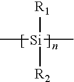
- An example of a bleachable main-chain polymer comprises polymers that are wholly, or at least partially composed of organo silicon compounds such as polysilanes having a structure:
- R 1 and R 2 represent from 1 to about 10 carbon atom alkyl, fluoroalkyl, alicyclic or aromatic groups and various combinations thereof.
- the n can range anywhere from about 4 to about 10,000, or from about 50 to about 1000.
- organo silicon based polymers useful in the invention comprise those described in U.S. Pat. Nos. 7,097,781; 7,008,749; 6,887,665; 6,770,417; 6,228,552; 6,054,254; 6,025,117; 4,871,646; 4,761,464 (also teaching organometallics comprising compounds having a polysilane copolymer backbone containing Ge, Sn, O and P); 4,588,801; and 4,587,205.
- a polysilane compound was prepared and studied where R 1 was methyl and R 2 was cyclohexyl (designated CyMeSi).
- CyMeSi cyclohexyl
- Another example is a compound where both R 1 and R 2 where n-hexyl (hex2Si).
- a change in the transmittance as a function of delivered dose is depicted in the FIGURE. As can be seen, the compounds progressively change their absorption properties during exposure to 193 nm light. They become more transparent.
- organic materials of the invention comprises polymers as noted before that are wholly or at least partially composed of aromatic hydroxyl and substituted aromatic hydroxyl compounds such as phenol, resorcinol, naphthol and the like reacted with a n organic carbonyl compound having from one to about five carbon atoms such as a ketone (e.g., acetone) or an aldehyde such as formaldehyde, and specifically include base catalyzed one-step and/or acid catalyzed two-step polymers.
- An example of a polymer suitable for the purposes of the invention comprises acid catalyzed phenol-formaldehyde polymers such as polymers from the novolak family and have the following structure:
- A represents one or multiple hydrogens, or from 1 to about 10 carbon atom single or multiple alkyl, fluoroalkyl, alicyclic, aromatic, halogen, alkoxy, carbonyl, carboxyl and other heteroatom-containing groups (e.g. sulfonates) and combinations thereof.
- the following references describe polymers of this type i.e., those based on various hydroxy aromatic compounds such as phenol cresols and naphthols polymerized with a carbonyl compound such as formaldehyde.
- polymers of the invention having photobleachable side chains comprises polymers that are wholly or at least partially composed of polystyrene or acrylate families having the following structure:
- X represents hydroxyl or a 1 to about 10 carbon alkoxy group
- B, C, D, E represent hydrogen, alkyl, fluoroalkyl, alicyclic, aromatic, alkoxy and other heteroatom-containing groups, halogen, and combinations thereof
- R represents hydrogen or a 1 to about 10 carbon alkyl group
- L represents a group linking the aromatic ring to the polymer backbone. It can be no group at all resulting in derivatives of polystyrene or it can be a group such as carboxyl resulting in a phenolic ester of an acrylic polymer, or a 1 to about 3 carbon alkylene, or oxygen resulting in derivatives of polyvinylether.
- the BMs of the invention are used as additives to the base polymer matrix of the top layer.
- the appropriate matrix polymer needs to be selected according to the MFR used.
- the BMs are miscible with the polymer and the polymer itself is completely or partially transparent to the MFR.
- These polymers are also selected to form stable films with uniform optical properties.
- polyacrylate or polymethacrylate (such as polymethylmethacrylate) resins are used as the matrix polymers for 193 nm litho processes. These polymers may also comprise polyvinylalcohol or polyvinylether based polymers as well as other polymers transparent to MFR.
- the CEL of the present invention comprising the cyclic compounds or organic compounds or combinations thereof such as CyMeSi or Hex2Si over the photoresist so that the cyclic compounds or organic compounds or combinations thereof simultaneously act as a CEL layer and a protection barrier or top antireflective coating or both, eliminating the need for additional top coats that are generally required especially in the case of current state-of-the-art immersion lithography schemes.
- This is included in the aspect of the invention referred to as operatively associating this CEL with the photoresist
- the bleachable moieties of the cyclic compounds or organic compounds or combinations thereof are directly incorporated into the photoresist eliminating the need to coat a separate CEL layer altogether.
- the cyclic compounds and organic compounds, and combinations thereof and other materials used with them of the present invention are physically mixed with the photoresist and/or polymerized into the photoresist. This is also included in the aspect of the invention referred to as operatively associating this CEL with the photoresist
- Operatively associating in this sense comprises forming a layer of the compound of the invention as described immediately above on an optical lithography surface or we form a mixture of such compound or compounds with the compound or composition employed to produce the optical lithography surface and form the mixture into a film.
- the components of the mixture include polymerizable groups, we form a polymeric combination of the components that make up the mixture.
- a photolithographic material comprising operatively associating a contrast enhancement layer made of the cyclic compounds or organic compounds of the invention or combinations thereof with a photoresist material, where operatively associating the contrast enhancement layer with the photoresist material comprises the process described immediately above.
- the compounds or compositions of the invention also include solvents such as glycol ethers; e.g., propylene glycol monomethyl ether acetate (PGMEA), toluene, and the like; photoacid generators (PAGs) such as triphenylsulphonium triflate, diphenyliodonium triflate, bis-4-t-butylphenyl iodonium triflate, norbornene dicarboximidyl triflate, bis-4-t-butylphenyl iodonium perfluorooctane sulfonate and the like; photobase generators such as t-butoxy carbonyl (BOC) protected amines or carbamates; photodecomposable bases such as onium hydroxides; surfactants; crosslinkers such as Powder linkTM or typical epoxy resin crosslinkers such as HeloxyTM brand materials, e.g. HeloxyTM 107.
- solvents such as glycol ethers; e
- Step 1 The materials are applied over the photoresist layer in any way known to those skilled in the art, including, but not limited to, spin-coating, spraying, dipping, evaporation, drop-casting and the like.
- the resist in turn is applied over other underlying layers such as, but not limited to, antireflective and/or planarizing underlayers,
- Step 2 The film stack composed of (top-down) BM, photoresist, any other underlying film(s) is then processed further; two examples are baking and vacuum drying.
- Step 3 The above mentioned processed film stack is exposed to the main fabrication radiation such as, but not limited to, light having wavelength of 193 nm.
- the exposure is effected either through a mask reticle typical for current optical lithography, or by a direct-write approach typical for electron beam lithography.
- the irradiation is selected to affect the particular photochemistry of the resist.
- Step 4 The exposed film stack is processed as needed further but most preferably processed to recover the original opacity of the top layer where reversibly bleachable material (RBM) is used.
- RBM reversibly bleachable material
- Such processing may involve, baking, exposure to chemicals in solution or vapors, gases, magnetic, electric or electromagnetic field, or radiation of a wavelength(s) or type(s) different from the main fabrication radiation.
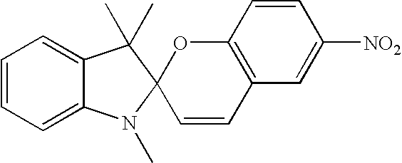
- photomers of dianthryl derivatives can be converted to the parent dianthryl derivative by 193 nm light.
- the reverse reaction can be accomplished by irradiating with UV light of wavelengths above 300 nm thereby forming the photomer again restoring the initial high absorption, for example:
- Step 5 The above steps are repeated in any sequence as needed for multiple exposure schemes as long as the RBM layer allows acceptable bleaching performance.
- the masks used for the exposures are repositioned as required or may comprise different masks altogether.
- Step 6 When all the above steps are completed any additional processing is performed as needed, such as baking at a higher temperature(s).
- Step 7 Subsequently, the top layer containing the BMs is removed in a separate processing step or it is removed during the development of the resist if employed.
- Step 8 The resist is developed using conventional techniques to generate a relief.
- Step 9 Other fabrication steps to produce a working device are applied as is typical in the semiconductor industry.
- 1,3-di(anthracene-9-yl)-1-propanone 150 mg was dissolved in benzene (175 mL) and irradiated for 30 min with 200 W high pressure Hg lamp that was surrounded by glass filter. Then the solvent was evaporated and the solid residue washed with ether and decanted twice. The solids were then recrystallized from hot mixture of benzene and hexanes. Obtained was 50 mg of pure photomer.
- the various numerical ranges describing the invention as set forth throughout the specification also include any combination of the lower ends of the ranges with the higher ends of the ranges, and any single numerical value within a range, or any single numerical value within a range that will reduce the scope of the lower limits of the range or the scope of the higher limits of the range, or both the lower ends and the higher ends of the ranges, and ranges falling within any of these ranges.
- the terms “about,” “substantial,” or “substantially,” when employed to define numerical parameters include, e.g., a variation up to five per-cent, up to ten per-cent, or up to 15 per-cent, or somewhat higher or lower than the upper limit of five per-cent, ten per-cent, or 15 per-cent.
- the term “up to” that defines numerical parameters means zero or a miniscule number, e.g. 0.001.
Abstract

where the radicals “R” and “Y” represent organo, or substituted organo moieties, Structures I, II, and III represent basic organic skeletons and can be unsubstituted or substituted in any available position with any one or combinations of multiple substituents.
Description

where R1 is methyl and R2 is cyclohexyl (CyMeSi), or both R1 and R2 are n-hexyl (Hex2Si).

where the R and Y represent organo, or substituted organo moieties. We subsequently describe these cyclic compounds in detail.


- where the R and Y represent organo, or substituted organo moieties;
- where R3, R4 represent hydrogen, alkyl, fluoroalkyl, alicyclic, aromatic, carbonyl, carboxyl and other heteroatom-containing groups and combinations thereof. As an example, R3 and R4 can be the same as in 1,4-dimethoxybenzene, or they can be different R3 being hydrogen and R4 being methyl as in 1-hydroxy-4-methoxybenzene. The can also be in different arrangement such as 1,3-dimethoxybenzene or 1,2-dimethoxybenzene;
- R5, R6, R7, R8, F, G represent independently hydrogen, 1 to about nine carbon atom alkyl, fluoroalkyl, alicyclic, aromatic, alkoxyl, carbonyl, and carboxyl, or halogen and other heteroatom-containing groups such as but not limited to cyano or nitro groups and combinations thereof;
- R9, R10, R11 represent hydrogen, 1 to about 9 carbon atom alkyl, fluoroalkyl, alicyclic and aromatic groups and various combinations thereof. R14 represents any kind of tethering group that physically connects the two aromatic rings together;
the tethering group can be comprised of 1 to about 8 methylene groups, more preferably 1 to 3 methylene groups such as in 1,3-diphenylpropane; any number can be replaced by other substituents such as carbonyl group as in 1,3-diphenyl-2-propanone; - R7 and R8 can also constitute a tethering group as describer for R14. Paracyclophan is an example of a compound having R14 and R7 and R8 groups in its molecule;
- Ar1 and Ar2 represent various aromatic substituents such as but not limited to substituted or unsubstituted phenyl or thienyl; they can be arranged in cis or trans geometry around the central double bond. Substituents R5 and R6 as well as R7 and R8 can also represent a 1 to about 9 carbon atom cyclic structure annulated to the base structure depicted in the corresponding formula; structures I, II, and III represent the basic skeletons and can be substituted in any available positions with any one or combinations of multiple substituents as described for R3 through R14; they can be e.g. methyl, ethyl, methoxy, hydroxyl, trifluoromethyl and acetyl to name few; specific examples of structure III are photomers of the following compounds of 1,3-diathryl-1 propanone, 1,3-dintryl-2-propanol or 1,3-dianthryl-ethane. These photomers and other anthracene photodimers and their syntheses are well known (Becker, Chem. Rev. 1993, 93,145).

where R1 and R2 represent from 1 to about 10 carbon atom alkyl, fluoroalkyl, alicyclic or aromatic groups and various combinations thereof. The n can range anywhere from about 4 to about 10,000, or from about 50 to about 1000. Examples of these and other organo silicon based polymers useful in the invention comprise those described in U.S. Pat. Nos. 7,097,781; 7,008,749; 6,887,665; 6,770,417; 6,228,552; 6,054,254; 6,025,117; 4,871,646; 4,761,464 (also teaching organometallics comprising compounds having a polysilane copolymer backbone containing Ge, Sn, O and P); 4,588,801; and 4,587,205. U.S. Pat. No. 6,887,665 cites two references in this regard; Hofer et al., “Contrast enhanced uv lithography with polysilanes,” SPIE VOL. 469 Advances in Resist Technology 108-116 (1984), and West et al., “Contrast enhanced Photolithography: Application of Photobleaching Process in Microlithography” Journal of Imaging Science 30: 65-68 (1986). The following references also show polysilanes: U.S. Pat. Nos. 5,776,764; 5,391,442; 5,039,593; and 4,820,788. However, none of these addresses use of polysilanes with 193 nm light.

where A represents one or multiple hydrogens, or from 1 to about 10 carbon atom single or multiple alkyl, fluoroalkyl, alicyclic, aromatic, halogen, alkoxy, carbonyl, carboxyl and other heteroatom-containing groups (e.g. sulfonates) and combinations thereof. The following references describe polymers of this type i.e., those based on various hydroxy aromatic compounds such as phenol cresols and naphthols polymerized with a carbonyl compound such as formaldehyde. U.S. Pat. Nos. 6,887,665; 6,770,417; 6,228,552; 6,228,552; 4,990,665; and 4,859,789.

where X represents hydroxyl or a 1 to about 10 carbon alkoxy group and B, C, D, E represent hydrogen, alkyl, fluoroalkyl, alicyclic, aromatic, alkoxy and other heteroatom-containing groups, halogen, and combinations thereof, R represents hydrogen or a 1 to about 10 carbon alkyl group and L represents a group linking the aromatic ring to the polymer backbone. It can be no group at all resulting in derivatives of polystyrene or it can be a group such as carboxyl resulting in a phenolic ester of an acrylic polymer, or a 1 to about 3 carbon alkylene, or oxygen resulting in derivatives of polyvinylether. The following references describe various acrylates and/or styrene polymers and copolymers: U.S. Pat. Nos. 6,586,156 (acrylate or methacrylate silane polymers); 6,387,593; 6,228,552; 4,990,665; and 4,859,789. Other styrene or acrylate polymers and/or copolymers suitable for the purpose of this invention comprise those described in U.S. Pat. Nos. 6,586,156; 6,387,593; 6,228,552; 4,990,665; and 4,859,789.


Claims (26)


Priority Applications (1)
| Application Number | Priority Date | Filing Date | Title |
|---|---|---|---|
| US11/698,182 US7875408B2 (en) | 2007-01-25 | 2007-01-25 | Bleachable materials for lithography |
Applications Claiming Priority (1)
| Application Number | Priority Date | Filing Date | Title |
|---|---|---|---|
| US11/698,182 US7875408B2 (en) | 2007-01-25 | 2007-01-25 | Bleachable materials for lithography |
Publications (2)
| Publication Number | Publication Date |
|---|---|
| US20080182178A1 US20080182178A1 (en) | 2008-07-31 |
| US7875408B2 true US7875408B2 (en) | 2011-01-25 |
Family
ID=39668378
Family Applications (1)
| Application Number | Title | Priority Date | Filing Date |
|---|---|---|---|
| US11/698,182 Expired - Fee Related US7875408B2 (en) | 2007-01-25 | 2007-01-25 | Bleachable materials for lithography |
Country Status (1)
| Country | Link |
|---|---|
| US (1) | US7875408B2 (en) |
Cited By (2)
| Publication number | Priority date | Publication date | Assignee | Title |
|---|---|---|---|---|
| US20090253072A1 (en) * | 2008-04-01 | 2009-10-08 | Petruska Melissa A | Nanoparticle reversible contrast enhancement material and method |
| US20210384443A1 (en) * | 2018-09-27 | 2021-12-09 | Merck Patent Gmbh | Compounds that can be used in an organic electronic device as active compounds |
Families Citing this family (2)
| Publication number | Priority date | Publication date | Assignee | Title |
|---|---|---|---|---|
| US7736825B2 (en) * | 2005-06-02 | 2010-06-15 | Asml Holding N.V. | Lithographic apparatus and device manufacturing method utilizing a resettable or reversible contrast enhancing layer in a multiple exposure system |
| EP2216683B1 (en) * | 2009-02-08 | 2018-11-14 | Rohm and Haas Electronic Materials, L.L.C. | Substrates coated with an antireflective composition and a photoresist |
Citations (43)
| Publication number | Priority date | Publication date | Assignee | Title |
|---|---|---|---|---|
| US4485168A (en) * | 1981-08-28 | 1984-11-27 | Sony Corporation | Photochromic photosensitive composition |
| US4491628A (en) | 1982-08-23 | 1985-01-01 | International Business Machines Corporation | Positive- and negative-working resist compositions with acid generating photoinitiator and polymer with acid labile groups pendant from polymer backbone |
| US4587205A (en) | 1984-04-05 | 1986-05-06 | The United States Of America As Represented By The United States Department Of Energy | Method of using polysilane positive photoresist materials |
| US4588801A (en) | 1984-04-05 | 1986-05-13 | The United States Of America As Represented By The United States Department Of Energy | Polysilane positive photoresist materials and methods for their use |
| US4677049A (en) | 1983-09-28 | 1987-06-30 | General Electric Company | Spin castable photobleachable layer forming compositions |
| US4702996A (en) | 1983-09-28 | 1987-10-27 | General Electric Company | Method of enhancing the contrast of images and materials therefor |
| US4761464A (en) | 1986-09-23 | 1988-08-02 | Zeigler John M | Interrupted polysilanes useful as photoresists |
| US4820788A (en) | 1986-10-31 | 1989-04-11 | John M. Zeigler | Poly(silyl silane)homo and copolymers |
| US4859789A (en) | 1982-11-01 | 1989-08-22 | General Electric Company | Diarylnitrones |
| US4871646A (en) | 1987-05-21 | 1989-10-03 | Kabushiki Kaisha Toshiba | Polysilane compound and photosensitive composition |
| US4942113A (en) | 1986-03-27 | 1990-07-17 | Plessey Overseas Limited | Contrast enhanced photolithography |
| US4990665A (en) | 1982-11-01 | 1991-02-05 | Microsi, Inc. | Diarylnitrones |
| US5039593A (en) | 1986-10-31 | 1991-08-13 | Zeigler John K | Poly(silyl silane) homo and copolymers |
| US5108874A (en) | 1982-11-01 | 1992-04-28 | Microsi, Inc. | Composite useful in photolithography |
| US5128230A (en) | 1986-12-23 | 1992-07-07 | Shipley Company Inc. | Quinone diazide containing photoresist composition utilizing mixed solvent of ethyl lactate, anisole and amyl acetate |
| US5391442A (en) | 1992-01-14 | 1995-02-21 | Nippon Paint Co., Ltd. | Method of forming color pattern on a polysilane layer |
| US5627006A (en) | 1991-12-16 | 1997-05-06 | Wako Pure Chemical Industries, Ltd. | Resist material |
| US5776764A (en) | 1993-10-20 | 1998-07-07 | Nippon Paint Co., Ltd. | Polysilane type photosensitive resin composition and method for forming pattern using the same |
| US6025117A (en) | 1996-12-09 | 2000-02-15 | Kabushiki Kaisha Toshiba | Method of forming a pattern using polysilane |
| US6054254A (en) | 1997-07-03 | 2000-04-25 | Kabushiki Kaisha Toshiba | Composition for underlying film and method of forming a pattern using the film |
| US6228552B1 (en) | 1996-09-13 | 2001-05-08 | Kabushiki Kaisha Toshiba | Photo-sensitive material, method of forming a resist pattern and manufacturing an electronic parts using photo-sensitive material |
| US6274288B1 (en) | 1995-06-12 | 2001-08-14 | California Institute Of Technology | Self-trapping and self-focusing of optical beams in photopolymers |
| US6291110B1 (en) | 1997-06-27 | 2001-09-18 | Pixelligent Technologies Llc | Methods for transferring a two-dimensional programmable exposure pattern for photolithography |
| US6294313B1 (en) * | 1997-08-08 | 2001-09-25 | Dai Nippon Printing Co., Ltd. | Pattern forming body, pattern forming method, and their applications |
| US6586156B2 (en) | 2001-07-17 | 2003-07-01 | International Business Machines Corporation | Etch improved resist systems containing acrylate (or methacrylate) silane monomers |
| US6770417B2 (en) | 2000-09-01 | 2004-08-03 | Fujitsu Limited | Negative resist composition, process for forming resist patterns, and process for manufacturing electron device |
| US20040152011A1 (en) | 2002-12-09 | 2004-08-05 | Pixelligent Technologies Llc | Reversible photobleachable materials based on nano-sized semiconductor particles and their optical applications |
| US6787289B2 (en) * | 2001-12-21 | 2004-09-07 | Jsr Corporation | Radiation sensitive refractive index changing composition and refractive index changing method |
| US20050064347A1 (en) | 2003-09-24 | 2005-03-24 | Yao-Ting Wang | Frequency division multiplexing (FDM) lithography |
| US6887665B2 (en) | 1996-11-14 | 2005-05-03 | Affymetrix, Inc. | Methods of array synthesis |
| US20050250052A1 (en) * | 2004-05-10 | 2005-11-10 | Nguyen Khe C | Maskless lithography using UV absorbing nano particle |
| US7002452B2 (en) | 2000-11-24 | 2006-02-21 | Aisin Seiki Kabushiki Kaisha | Collision preventing apparatus for a vehicle |
| US7008749B2 (en) | 2001-03-12 | 2006-03-07 | The University Of North Carolina At Charlotte | High resolution resists for next generation lithographies |
| US7022452B2 (en) * | 2002-09-04 | 2006-04-04 | Agilent Technologies, Inc. | Contrast enhanced photolithography |
| US7087358B2 (en) * | 2000-06-06 | 2006-08-08 | Fuji Photo Film Co., Ltd. | Image-formation material and infrared absorber |
| US7097791B2 (en) | 2000-02-09 | 2006-08-29 | Netstal Maschinen Ag | Method of controlling/regulating an embossing procedure and drive control device for injection molding machines |
| US20070072110A1 (en) * | 2005-09-08 | 2007-03-29 | Xerox Corporation | Reimageable paper |
| US7205088B2 (en) * | 2004-04-29 | 2007-04-17 | Xerox Corporation | Reimageable medium with light absorbing material |
| US7214456B2 (en) * | 2004-04-29 | 2007-05-08 | Xerox Corporation | Reimageable medium |
| US20070105043A1 (en) * | 2005-10-21 | 2007-05-10 | Klaus Elian | Photosensitive coating for enhancing a contrast of a photolithographic exposure |
| US7291400B2 (en) * | 2002-03-20 | 2007-11-06 | Dai Nippon Printing Co., Ltd. | Decorative sheet |
| US7300727B2 (en) * | 2004-04-29 | 2007-11-27 | Xerox Corporation | Method for forming temporary image |
| US7521159B2 (en) * | 2005-03-30 | 2009-04-21 | Xerox Corporation | Multicolor electronic paper |
-
2007
- 2007-01-25 US US11/698,182 patent/US7875408B2/en not_active Expired - Fee Related
Patent Citations (44)
| Publication number | Priority date | Publication date | Assignee | Title |
|---|---|---|---|---|
| US4485168A (en) * | 1981-08-28 | 1984-11-27 | Sony Corporation | Photochromic photosensitive composition |
| US4491628A (en) | 1982-08-23 | 1985-01-01 | International Business Machines Corporation | Positive- and negative-working resist compositions with acid generating photoinitiator and polymer with acid labile groups pendant from polymer backbone |
| US4990665A (en) | 1982-11-01 | 1991-02-05 | Microsi, Inc. | Diarylnitrones |
| US5108874A (en) | 1982-11-01 | 1992-04-28 | Microsi, Inc. | Composite useful in photolithography |
| US4859789A (en) | 1982-11-01 | 1989-08-22 | General Electric Company | Diarylnitrones |
| US4677049A (en) | 1983-09-28 | 1987-06-30 | General Electric Company | Spin castable photobleachable layer forming compositions |
| US4702996A (en) | 1983-09-28 | 1987-10-27 | General Electric Company | Method of enhancing the contrast of images and materials therefor |
| US4587205A (en) | 1984-04-05 | 1986-05-06 | The United States Of America As Represented By The United States Department Of Energy | Method of using polysilane positive photoresist materials |
| US4588801A (en) | 1984-04-05 | 1986-05-13 | The United States Of America As Represented By The United States Department Of Energy | Polysilane positive photoresist materials and methods for their use |
| US4942113A (en) | 1986-03-27 | 1990-07-17 | Plessey Overseas Limited | Contrast enhanced photolithography |
| US4761464A (en) | 1986-09-23 | 1988-08-02 | Zeigler John M | Interrupted polysilanes useful as photoresists |
| US5039593A (en) | 1986-10-31 | 1991-08-13 | Zeigler John K | Poly(silyl silane) homo and copolymers |
| US4820788A (en) | 1986-10-31 | 1989-04-11 | John M. Zeigler | Poly(silyl silane)homo and copolymers |
| US5128230A (en) | 1986-12-23 | 1992-07-07 | Shipley Company Inc. | Quinone diazide containing photoresist composition utilizing mixed solvent of ethyl lactate, anisole and amyl acetate |
| US4871646A (en) | 1987-05-21 | 1989-10-03 | Kabushiki Kaisha Toshiba | Polysilane compound and photosensitive composition |
| US5627006A (en) | 1991-12-16 | 1997-05-06 | Wako Pure Chemical Industries, Ltd. | Resist material |
| US5391442A (en) | 1992-01-14 | 1995-02-21 | Nippon Paint Co., Ltd. | Method of forming color pattern on a polysilane layer |
| US5776764A (en) | 1993-10-20 | 1998-07-07 | Nippon Paint Co., Ltd. | Polysilane type photosensitive resin composition and method for forming pattern using the same |
| US6387593B1 (en) | 1995-06-12 | 2002-05-14 | California Institute Of Technology | Self-trapping and self-focusing of optical beams in photopolymers |
| US6274288B1 (en) | 1995-06-12 | 2001-08-14 | California Institute Of Technology | Self-trapping and self-focusing of optical beams in photopolymers |
| US6228552B1 (en) | 1996-09-13 | 2001-05-08 | Kabushiki Kaisha Toshiba | Photo-sensitive material, method of forming a resist pattern and manufacturing an electronic parts using photo-sensitive material |
| US6887665B2 (en) | 1996-11-14 | 2005-05-03 | Affymetrix, Inc. | Methods of array synthesis |
| US6025117A (en) | 1996-12-09 | 2000-02-15 | Kabushiki Kaisha Toshiba | Method of forming a pattern using polysilane |
| US6291110B1 (en) | 1997-06-27 | 2001-09-18 | Pixelligent Technologies Llc | Methods for transferring a two-dimensional programmable exposure pattern for photolithography |
| US6054254A (en) | 1997-07-03 | 2000-04-25 | Kabushiki Kaisha Toshiba | Composition for underlying film and method of forming a pattern using the film |
| US6294313B1 (en) * | 1997-08-08 | 2001-09-25 | Dai Nippon Printing Co., Ltd. | Pattern forming body, pattern forming method, and their applications |
| US7097791B2 (en) | 2000-02-09 | 2006-08-29 | Netstal Maschinen Ag | Method of controlling/regulating an embossing procedure and drive control device for injection molding machines |
| US7087358B2 (en) * | 2000-06-06 | 2006-08-08 | Fuji Photo Film Co., Ltd. | Image-formation material and infrared absorber |
| US6770417B2 (en) | 2000-09-01 | 2004-08-03 | Fujitsu Limited | Negative resist composition, process for forming resist patterns, and process for manufacturing electron device |
| US7002452B2 (en) | 2000-11-24 | 2006-02-21 | Aisin Seiki Kabushiki Kaisha | Collision preventing apparatus for a vehicle |
| US7008749B2 (en) | 2001-03-12 | 2006-03-07 | The University Of North Carolina At Charlotte | High resolution resists for next generation lithographies |
| US6586156B2 (en) | 2001-07-17 | 2003-07-01 | International Business Machines Corporation | Etch improved resist systems containing acrylate (or methacrylate) silane monomers |
| US6787289B2 (en) * | 2001-12-21 | 2004-09-07 | Jsr Corporation | Radiation sensitive refractive index changing composition and refractive index changing method |
| US7291400B2 (en) * | 2002-03-20 | 2007-11-06 | Dai Nippon Printing Co., Ltd. | Decorative sheet |
| US7022452B2 (en) * | 2002-09-04 | 2006-04-04 | Agilent Technologies, Inc. | Contrast enhanced photolithography |
| US20040152011A1 (en) | 2002-12-09 | 2004-08-05 | Pixelligent Technologies Llc | Reversible photobleachable materials based on nano-sized semiconductor particles and their optical applications |
| US20050064347A1 (en) | 2003-09-24 | 2005-03-24 | Yao-Ting Wang | Frequency division multiplexing (FDM) lithography |
| US7205088B2 (en) * | 2004-04-29 | 2007-04-17 | Xerox Corporation | Reimageable medium with light absorbing material |
| US7214456B2 (en) * | 2004-04-29 | 2007-05-08 | Xerox Corporation | Reimageable medium |
| US7300727B2 (en) * | 2004-04-29 | 2007-11-27 | Xerox Corporation | Method for forming temporary image |
| US20050250052A1 (en) * | 2004-05-10 | 2005-11-10 | Nguyen Khe C | Maskless lithography using UV absorbing nano particle |
| US7521159B2 (en) * | 2005-03-30 | 2009-04-21 | Xerox Corporation | Multicolor electronic paper |
| US20070072110A1 (en) * | 2005-09-08 | 2007-03-29 | Xerox Corporation | Reimageable paper |
| US20070105043A1 (en) * | 2005-10-21 | 2007-05-10 | Klaus Elian | Photosensitive coating for enhancing a contrast of a photolithographic exposure |
Cited By (2)
| Publication number | Priority date | Publication date | Assignee | Title |
|---|---|---|---|---|
| US20090253072A1 (en) * | 2008-04-01 | 2009-10-08 | Petruska Melissa A | Nanoparticle reversible contrast enhancement material and method |
| US20210384443A1 (en) * | 2018-09-27 | 2021-12-09 | Merck Patent Gmbh | Compounds that can be used in an organic electronic device as active compounds |
Also Published As
| Publication number | Publication date |
|---|---|
| US20080182178A1 (en) | 2008-07-31 |
Similar Documents
| Publication | Publication Date | Title |
|---|---|---|
| US5738975A (en) | Photosensitive resin and method for patterning by use of the same | |
| US5635332A (en) | Alkylsulfonium salts and photoresist compositions containing the same | |
| EP1465877B1 (en) | Positive-working photoimageable bottom antireflective coating | |
| US5866304A (en) | Photosensitive resin and method for patterning by use of the same | |
| TWI591057B (en) | Sulfonic acid derivative compounds as photoacid generators in resist applications | |
| TWI294990B (en) | Hydroxy-amino thermally cured undercoat for 193 nm lithography | |
| TWI386759B (en) | Positive resist composition and pattern forming method utilizing the same | |
| CN102227680A (en) | Photosensitive composition | |
| JPH0827102A (en) | Sulfontium chloide having cross-linked cyclic alkyl group, optical acid generator, photosesitive resin composition containing the same and pattern formation using the resin | |
| CN1443315A (en) | Photoresist composition for deep UV and process thereof | |
| JP2007231270A (en) | Polymer for organic anti-reflection film and its production method and semi-conductor device | |
| TW201011078A (en) | An antireflective coating composition | |
| JPS62234148A (en) | Light fading layer for enhancing contrast | |
| KR20180041201A (en) | In the resist application, a sulfonic acid derivative compound | |
| JP4102010B2 (en) | Composition for organic antireflection film and method for producing the same | |
| JP3907197B2 (en) | Thiophene-containing photoacid generator for photolithography | |
| CN111948904A (en) | Photoresist composition, method for forming photolithographic pattern using the same, and use thereof | |
| US7875408B2 (en) | Bleachable materials for lithography | |
| JP4002057B2 (en) | Composition for organic antireflection film and organic antireflection film pattern forming method | |
| JP2022184974A (en) | Cyclic sulfonic acid ester compounds as photoacid generators in resist applications | |
| JP2965016B2 (en) | Photosensitive resin composition for far ultraviolet exposure and pattern forming method using the same | |
| McCullough et al. | Polydimethylglutarimide (PMGI) resist-a progress report | |
| KR100974587B1 (en) | Anti-reflective composition | |
| CN117311087A (en) | Ultraviolet photoresist and ultraviolet photoresist patterning method | |
| Ekhorutomwen et al. | Critical review on photoresists |
Legal Events
| Date | Code | Title | Description |
|---|---|---|---|
| AS | Assignment |
Owner name: INTERNATIONAL BUSINESS MACHINES, INC., NEW YORK Free format text: ASSIGNMENT OF ASSIGNORS INTEREST;ASSIGNORS:HOFFNAGLE, JOHN A.;MEDEIROS, DAVID R.;MILLER, ROBERT D.;AND OTHERS;REEL/FRAME:019405/0951;SIGNING DATES FROM 20070504 TO 20070522 Owner name: INTERNATIONAL BUSINESS MACHINES, INC., NEW YORK Free format text: ASSIGNMENT OF ASSIGNORS INTEREST;ASSIGNORS:HOFFNAGLE, JOHN A.;MEDEIROS, DAVID R.;MILLER, ROBERT D.;AND OTHERS;SIGNING DATES FROM 20070504 TO 20070522;REEL/FRAME:019405/0951 |
|
| REMI | Maintenance fee reminder mailed | ||
| FPAY | Fee payment |
Year of fee payment: 4 |
|
| SULP | Surcharge for late payment | ||
| AS | Assignment |
Owner name: GLOBALFOUNDRIES U.S. 2 LLC, NEW YORK Free format text: ASSIGNMENT OF ASSIGNORS INTEREST;ASSIGNOR:INTERNATIONAL BUSINESS MACHINES CORPORATION;REEL/FRAME:036550/0001 Effective date: 20150629 |
|
| AS | Assignment |
Owner name: GLOBALFOUNDRIES INC., CAYMAN ISLANDS Free format text: ASSIGNMENT OF ASSIGNORS INTEREST;ASSIGNORS:GLOBALFOUNDRIES U.S. 2 LLC;GLOBALFOUNDRIES U.S. INC.;REEL/FRAME:036779/0001 Effective date: 20150910 |
|
| FEPP | Fee payment procedure |
Free format text: MAINTENANCE FEE REMINDER MAILED (ORIGINAL EVENT CODE: REM.); ENTITY STATUS OF PATENT OWNER: LARGE ENTITY |
|
| AS | Assignment |
Owner name: WILMINGTON TRUST, NATIONAL ASSOCIATION, DELAWARE Free format text: SECURITY AGREEMENT;ASSIGNOR:GLOBALFOUNDRIES INC.;REEL/FRAME:049490/0001 Effective date: 20181127 |
|
| LAPS | Lapse for failure to pay maintenance fees |
Free format text: PATENT EXPIRED FOR FAILURE TO PAY MAINTENANCE FEES (ORIGINAL EVENT CODE: EXP.); ENTITY STATUS OF PATENT OWNER: LARGE ENTITY |
|
| STCH | Information on status: patent discontinuation |
Free format text: PATENT EXPIRED DUE TO NONPAYMENT OF MAINTENANCE FEES UNDER 37 CFR 1.362 |
|
| FP | Lapsed due to failure to pay maintenance fee |
Effective date: 20190125 |
|
| AS | Assignment |
Owner name: GLOBALFOUNDRIES INC., CAYMAN ISLANDS Free format text: RELEASE BY SECURED PARTY;ASSIGNOR:WILMINGTON TRUST, NATIONAL ASSOCIATION;REEL/FRAME:054636/0001 Effective date: 20201117 |
|
| AS | Assignment |
Owner name: GLOBALFOUNDRIES U.S. INC., NEW YORK Free format text: RELEASE BY SECURED PARTY;ASSIGNOR:WILMINGTON TRUST, NATIONAL ASSOCIATION;REEL/FRAME:056987/0001 Effective date: 20201117 |