US7851260B2 - Method for manufacturing a semiconductor device - Google Patents
Method for manufacturing a semiconductor device Download PDFInfo
- Publication number
- US7851260B2 US7851260B2 US12/332,146 US33214608A US7851260B2 US 7851260 B2 US7851260 B2 US 7851260B2 US 33214608 A US33214608 A US 33214608A US 7851260 B2 US7851260 B2 US 7851260B2
- Authority
- US
- United States
- Prior art keywords
- resin
- substrate
- semiconductor device
- cutting
- manufacturing
- Prior art date
- Legal status (The legal status is an assumption and is not a legal conclusion. Google has not performed a legal analysis and makes no representation as to the accuracy of the status listed.)
- Expired - Fee Related, expires
Links
Images


Classifications
-
- H—ELECTRICITY
- H01—ELECTRIC ELEMENTS
- H01L—SEMICONDUCTOR DEVICES NOT COVERED BY CLASS H10
- H01L21/00—Processes or apparatus adapted for the manufacture or treatment of semiconductor or solid state devices or of parts thereof
- H01L21/02—Manufacture or treatment of semiconductor devices or of parts thereof
- H01L21/04—Manufacture or treatment of semiconductor devices or of parts thereof the devices having at least one potential-jump barrier or surface barrier, e.g. PN junction, depletion layer or carrier concentration layer
- H01L21/50—Assembly of semiconductor devices using processes or apparatus not provided for in a single one of the subgroups H01L21/06 - H01L21/326, e.g. sealing of a cap to a base of a container
- H01L21/56—Encapsulations, e.g. encapsulation layers, coatings
- H01L21/561—Batch processing
-
- H—ELECTRICITY
- H01—ELECTRIC ELEMENTS
- H01L—SEMICONDUCTOR DEVICES NOT COVERED BY CLASS H10
- H01L24/00—Arrangements for connecting or disconnecting semiconductor or solid-state bodies; Methods or apparatus related thereto
- H01L24/93—Batch processes
- H01L24/95—Batch processes at chip-level, i.e. with connecting carried out on a plurality of singulated devices, i.e. on diced chips
- H01L24/97—Batch processes at chip-level, i.e. with connecting carried out on a plurality of singulated devices, i.e. on diced chips the devices being connected to a common substrate, e.g. interposer, said common substrate being separable into individual assemblies after connecting
-
- H—ELECTRICITY
- H01—ELECTRIC ELEMENTS
- H01L—SEMICONDUCTOR DEVICES NOT COVERED BY CLASS H10
- H01L2924/00—Indexing scheme for arrangements or methods for connecting or disconnecting semiconductor or solid-state bodies as covered by H01L24/00
- H01L2924/15—Details of package parts other than the semiconductor or other solid state devices to be connected
- H01L2924/151—Die mounting substrate
- H01L2924/153—Connection portion
- H01L2924/1531—Connection portion the connection portion being formed only on the surface of the substrate opposite to the die mounting surface
- H01L2924/15311—Connection portion the connection portion being formed only on the surface of the substrate opposite to the die mounting surface being a ball array, e.g. BGA
-
- H—ELECTRICITY
- H01—ELECTRIC ELEMENTS
- H01L—SEMICONDUCTOR DEVICES NOT COVERED BY CLASS H10
- H01L2924/00—Indexing scheme for arrangements or methods for connecting or disconnecting semiconductor or solid-state bodies as covered by H01L24/00
- H01L2924/15—Details of package parts other than the semiconductor or other solid state devices to be connected
- H01L2924/181—Encapsulation
-
- H—ELECTRICITY
- H01—ELECTRIC ELEMENTS
- H01L—SEMICONDUCTOR DEVICES NOT COVERED BY CLASS H10
- H01L2924/00—Indexing scheme for arrangements or methods for connecting or disconnecting semiconductor or solid-state bodies as covered by H01L24/00
- H01L2924/30—Technical effects
- H01L2924/35—Mechanical effects
- H01L2924/351—Thermal stress
- H01L2924/3511—Warping
Definitions
- the present invention relates to methods for manufacturing a semiconductor device.
- JP-A-4-313245 discloses a method for manufacturing a semiconductor device that includes curing the semiconductor device, after it is molded with resin, while applying a pressure to hold it flat.
- the semiconductor device In a single-side molded package that is typical for a ball grid array (BGA), only a surface of a substrate where a semiconductor chip is mounted thereon is molded with resin. Accordingly, the semiconductor device has a double layered structure that includes the substrate and the resin. It should be appreciated that because of the difference in coefficient of thermal expansion between the substrate and the resin, during the heating processes associated with the aforementioned molding and curing operations, warpage in the semiconductor device occurs. When warpage is large, errors in delivery and by adsorption to jigs in a later process may result. As a result, yield rate is decreased and the cost of the semiconductor device is increased.
- BGA ball grid array
- slits are provided on a substrate, to divide the resin into smaller divisions.
- the use of the substrate and the resin is less efficient which results in a higher cost.
- warpage increases.
- a method for manufacturing a semiconductor device is disclosed. As a part of the method, one surface of a substrate is molded with resin where the substrate and the resin are heated in a first heating process and are maintained in a flat condition. The substrate and the resin are returned to room temperature while being maintained in the flat condition after the first heating process. The resin is cut after the substrate and the resin are returned to room temperature from a surface of the resin that is opposite the surface of the resin where the substrate contacts the resin. The substrate is left intact when the resin is cut. Thereafter, the substrate is separated.
- FIG. 1 is a flowchart showing steps in a manufacturing process of a semiconductor device of a first comparative example.
- FIG. 2 is a side view illustrating a semiconductor device having warpage.
- FIG. 3 is a flowchart showing steps in a manufacturing process of a semiconductor device of a second comparative example.
- FIG. 4A is a side view illustrating a manufacturing process of a semiconductor device of the second comparative example.
- FIG. 4B is a side view illustrating a manufacturing process of a semiconductor device according to a second comparative example.
- FIG. 4C is a side view illustrating the manufacturing process of the semiconductor device of the second comparative example.
- FIG. 5A is a side view illustrating a measuring method of warpage.
- FIG. 5B is a side view illustrating a method of measuring warpage.
- FIG. 5C is a side view illustrating a measuring method of warpage.
- FIG. 6 is a perspective view illustrating a sample in a first experiment.
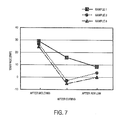
- FIG. 7 is a graph showing results of the first experiment.
- FIG. 8 is a flowchart that shows steps in a manufacturing process of a semiconductor device of a first embodiment of the present invention.
- FIG. 9A is a side view illustrating the manufacturing process of the semiconductor device of the first embodiment.
- FIG. 9B is a side view illustrating the manufacturing process of the semiconductor device of the first embodiment.
- FIG. 9C is a side view illustrating the manufacturing process of the semiconductor device of the first embodiment.
- FIG. 9D is a side view illustrating the manufacturing process of the semiconductor device of the first embodiment.
- FIG. 10 is a top view showing a positional relationship between cutting plane lines.
- FIG. 11A is a side view illustrating a second experiment according to one embodiment.
- FIG. 11B is a side view illustrating a second experiment according to one embodiment.
- FIG. 11C is a side view illustrating a second experiment according to one embodiment.
- FIG. 11D is a side view illustrating a second experiment according to one embodiment.
- FIG. 12 is a graph showing results of a third experiment according to one embodiment.
- FIG. 13A is a top view of the semiconductor device according to one embodiment.
- FIG. 13B is a top view of a semiconductor device according to another embodiment.
- a first comparative example is an example of molding one surface of a substrate with resin and carrying out an ordinary curing process.
- FIGS. 1 and 2 a method for manufacturing a semiconductor device of the first comparative example will be described.
- FIG. 1 is a flowchart that shows a process flow involved in forming a semiconductor device of the first comparative example according to one embodiment.
- FIG. 2 is a side view illustrating a semiconductor device when warpage has occurred.
- step S 10 by molding a surface of an insulating substrate 10 composed of, for example glass epoxy, where a semiconductor chip (not shown) is mounted with a resin 20 having a thermosetting property composed of, for example epoxy, a semiconductor device 100 is formed.
- the molding process includes heating the insulating substrate 10 and the resin 20 to, for example, 175 degrees Celsius (a third heating process).
- a third heating process in order to remove residual stress of the molded resin 20 , the insulating substrate 10 and the resin 20 are heated, for example, at 175 degrees Celsius for 5 hours (a first heating process) and, thereafter, are brought back to room temperature.
- heating is carried out at a temperature equal to or higher than that used in the molding process.
- step S 12 terminals 12 (not shown) composed of, for example, solder are disposed on the insulating substrate 10 .
- step S 13 a reflow process is carried out to fix the terminals 12 onto the insulating substrate 10 .
- the reflow process includes heating the insulating substrate 10 , the resin 20 , and the terminals 12 to, for example, 240degrees Celsius (a second heating process).
- step S 14 the insulating substrate 10 and the resin 20 are cut, for example, in 8 mm divisions, and are accordingly separated.
- the semiconductor device 100 has a double layered structure composed of the insulating substrate 10 and the resin 20 . Because of the difference between the coefficient of thermal expansion of the insulating substrate 10 and that of the resin 20 , when heated in the molding process in step S 10 , warpage such as is shown in FIG. 2 occurs. With the semiconductor device 100 exhibiting a large warpage, for example, in the terminal disposition process in step S 12 , errors related to delivery and adsorption to jigs may result.
- FIG. 3 is a flowchart that shows steps in a process for forming a semiconductor device according to a second comparative example.
- FIGS. 4A to 4C are side views illustrating respective operations corresponding to step S 21 to step S 23 . It should be appreciated that the illustration of step S 20 is the same as that shown in FIG. 2 .
- step S 20 shown in FIG. 3 a molding process is carried out to form a semiconductor device 110 (the semiconductor device 100 in the first comparative example is replaced with the semiconductor device 110 in the second comparative example).
- step S 21 as shown in FIG. 4A a pressure curing process is carried out.
- the insulating substrate 10 and the resin 20 are heated while a pressure is applied by putting a weight of, for example, 10 kg thereon to hold them in a flat condition. Thereafter, while being held flat, the insulating substrate 10 and the resin 20 are brought back to room temperature.
- step S 22 as shown in FIG. 4B , on the insulating substrate 10 , the terminals 12 are disposed.
- step S 23 as shown in FIG. 4C a reflow process is carried out to fix the terminals 12 onto the insulating substrate 10 .
- step S 24 separation of the insulation substrate 10 and the resin 20 is carried out.
- step S 21 by performing the pressure curing process in step S 21 , the warpage that occurred in the molding process in step S 20 is corrected.
- the reflow process in step S 23 is a process to heat, as shown in FIG. 4C , the warpage is restored. Therefore, with that of a large warpage, an error occurs in the separation process in step S 24 .
- the warpage is restored.
- FIG. 5A is a side view illustrating, when a sample is placed on a plane surface with the insulating substrate 10 positioned face down, a type of warpage that occurs in a direction in which the center of the insulating substrate 10 is in contact with the plane surface and both ends thereof are separated from (extend above) the plane surface.
- the warpage in this case is defined (when one end of the bottom surface of the insulating substrate 10 is in contact with the plane surface as shown in FIG. 5B ) by the height H 1 that the other end extends from the plane surface, and is represented by a positive value.
- FIG. 5C is a side view illustrating, when a sample is placed on the plane surface with the insulating substrate 10 face down, a type of warpage that occurs in a direction in which both ends of the insulating substrate 10 are in contact with the plane surface and the center thereof is separated from the plane surface.
- the warpage in this case is defined, when both ends of the bottom surface of the insulating substrate 10 are in contact with the plane surface, by the height H 2 at the center of the insulating substrate 10 measured from the plane surface to the substrate, and is represented by a negative value.
- the first experiment is a comparison among first, second and third samples, where a first sample uses an ordinary curing process that is performed without the application of any pressure, and a second and a third sample uses curing processes that are respectively carried out using the application of pressure.
- FIG. 6 is a perspective view of the first sample used in the first experiment.
- the dimensions of the insulating substrate 10 include a length L of 230 mm, a width D of 62 mm, and a thickness H of 180 ⁇ m.
- the resin 20 molds one surface of the insulating substrate 10 and has a thickness H′ of 450 ⁇ m.
- the insulating substrate 10 is composed of glass epoxy, the resin 20 is composed of epoxy, and the terminals 12 (see FIGS. 9B-9D ) are composed of solder.
- the second and the third samples have the same dimensions and materials as the first sample.
- each of the samples was heated to 175 degrees Celsius and subsequently the warpage thereof measured. Thereafter, a curing process was carried out on the first sample without applying any pressure. On the second and the third samples, weights of 1.5 kg and 10 kg were respectively placed thereon and respective curing processes carried out. The curing processes were processes that involve applying heat at 175 degrees Celsius for 5 hours and returning the sample to room temperature. After the curing process, the warpage of each of the samples was measured. Each of the samples were heated to 240 degrees Celsius as a part of a reflow process and the warpage was measured.
- FIG. 7 is a graph showing the respective warpage values of each of the samples after the molding, curing and reflow processes.
- the respective warpage of the first to the third samples were about 30 mm and similar in degrees.
- the warpage of the first sample on which the curing process has been carried out without the application of pressure was 15 mm.
- the respective warpage of the second and the third samples on which the pressure curing process have been carried out were about ⁇ 3 mm. This shows that by performing a pressure curing process, warpage can be reduced. Subsequently, after performing the reflow process, the warpage of the first sample was about 8 mm.
- the warpage of the second and the third samples respectively were about 5 mm and about 0 mm, being increased from the warpage that is exhibited after the pressure curing process. From this result, it shows that, regardless of the weight applied during the curing process, the warpage which is temporarily corrected by the pressure curing process is restored by heating in the reflow process.
- FIG. 8 shows a process flow of the semiconductor device of the first embodiment.
- FIGS. 9A to 9D are side views illustrating respective cross sections associated with step S 32 to step S 35 .
- the illustrations of steps S 30 and S 31 are the same as those respectively shown in FIG. 2 and FIG. 4A .
- FIG. 10 is a top view illustrating a cutting plane line 22 associated with the half-cutting process and a cutting plane line 24 associated with a separation process.
- a solid line represents the cutting plane line 22 and a broken line represents the cutting plane line 24 .
- step S 30 shown in FIG. 8 a molding process is performed to form a semiconductor device 120 (the semiconductor device 100 in the first comparative example is replaced with the semiconductor device 120 in the first embodiment).
- step S 31 a pressure curing process is performed. As shown in FIG. 4A , by carrying out the pressure curing process, the warpage of the semiconductor device 120 is corrected (the semiconductor device 110 in the second comparative example is replaced with the semiconductor device 120 in the first embodiment).
- step S 32 as shown in FIG. 9A the half-cutting process that is executed to cut the resin 20 is performed.
- This process is a process, using a blade having a width of, for example 40 ⁇ m, to cut from a surface opposite the surface where the resin 20 contacts the insulating substrate 10 , and along the cutting plane line 22 , such that only the resin 20 is cut in a width direction so as to leave the insulating substrate 10 intact.
- the width of the cutting plane line 22 may be 40 ⁇ m. In other embodiments other widths may be used.
- step S 33 as shown in FIG. 9B the terminals 12 are disposed on the insulating substrate 10 .
- step S 34 as shown in FIG. 9C
- a reflow process is carried out to form the terminals 12 .
- step S 35 as shown in FIG. 9D with a blade having a width of, for example 250 ⁇ m, the insulating substrate 10 and the resin 20 are cut along the cutting plane line 24 , and in this manner the insulating substrate 10 is separated.
- the width of the cutting plane line 22 may be 250 ⁇ m. In other embodiments other widths may be used.
- the aforementioned cutting operations separates semiconductor device 120 a.
- the warpage is temporarily corrected. Thereafter, in step S 32 , the half-cutting process is carried out to cut the resin 20 into small pieces. As shown in FIG. 9C , the warpage restored in the reflow process in step S 34 occurs in each of the small pieces of the resin 20 . Therefore, the warpage can be reduced from the warpage that occurs where and undivided insulating substrate 10 is processed as shown in the first and the second comparative examples. Accordingly, errors in delivery and by adsorption in the separation process in step S 35 can be prevented. Consequently, the yield rate can be improved and cost reduction can be achieved.
- a method is provided to control warpage by providing slits in the insulating substrate 10 so as to divide the resin into small areas or divisions.
- the resin 20 is divided into small pieces in the half-cutting process in step S 32 , it is not necessary to provide slits to the insulating substrate 10 .
- the insulating substrate 10 can be made larger. Therefore, the efficiency in the use of the insulating substrate 10 and the resin 20 is improved. Consequently, cost reduction can be achieved.
- the position of the cutting plane line 22 in the half-cutting process in step S 32 and the position of the cutting plane line 24 in the separation process in step S 35 are not limited as such. However, as shown in FIG. 10 , in order not to affect the number of separated semiconductor devices 120 a obtainable from the semiconductor device 120 in the half-cutting process, it is preferable that a plurality of cutting plane lines 22 in the half-cutting process overlaps with at least one of a plurality of cutting plane lines 24 in the separation process.
- the width of the cutting plane line 22 in the half-cutting process and that of the cutting plane line 24 in the separation process of the insulating substrate 10 are not limited as such. However, as shown in FIG. 9D , in order for a cutting plane 26 of the insulating substrate 10 and a cutting plane 28 of the resin 20 to be in the same plane after the separation process, it is preferable that the width W 1 of the cutting plane line 22 in the half-cutting process is smaller than the width W 2 of the cutting plane line 24 in the separation process. More specifically, it is preferable that the cutting plane line 24 in the separation process includes the cutting plane line 22 in the half-cutting process.
- FIGS. 11A to 11D are side views of the fourth sample viewed from a direction of an arrow 30 shown in FIG. 6 , while FIG. 11A illustrates step S 30 , FIG. 11B illustrates step S 31 , FIG. 11C illustrates step S 32 , and FIG. 11D illustrates step S 34 .
- the molding process may be performed by heating the insulating substrate 10 and the resin 20 to 175 degrees Celsius. In other embodiments other temperatures can be used.
- FIG. 11A in the molding process, when the fourth sample was placed on a plane surface with the insulating substrate 10 face down, the warpage occurred in a direction in which the center of the insulating substrate 10 was in contact with the plane surface and both ends thereof were separated from the plane surface. In this example, the warpage after the molding process was 27 mm. In other embodiments, other warpage values can be obtained.
- step S 31 as shown in FIG. 11B the pressure curing process is performed, with a weight placed on the fourth sample to hold it in a flat condition, by heating it at 175 degrees Celsius for 5 hours and then by return it back to room temperature while being maintained in a flat condition. In other embodiments other temperatures and times may be used.
- the warpage after the pressure curing process was ⁇ 4 mm.
- step S 32 as shown in FIG. 11C the half-cutting process to cut the resin 20 is performed.
- the thickness of the blade used for cutting more specifically, the width of the cutting plane line of the resin 20 was 100 ⁇ m.
- the resin 20 was cut in every 8 mm in a width direction. In other embodiments other widths may be used. After the half-cutting process, the warpage may hardly be recognizable.
- step S 33 the terminals 12 composed of solder are disposed on the insulating substrate 10 .
- step S 34 as shown in FIG. 11D , by heating the fourth sample to 240 degrees Celsius, the reflow process is performed. After the reflow process, similar to that after the half-cutting process, the warpage was hardly recognizable either.
- the warpage was reduced from 27 mm to ⁇ 4 mm.
- the warpage is nearly eliminated.
- the warpage is hardly recognizable and not much changed from that of before the reflow process. More specifically, by performing the half-cutting process, the warpage was prevented from restoring.
- a third experiment is a comparison between a fifth sample fabricated without the half-cutting process being performed and a sixth sample carried out using the half-cutting process.
- the samples used in the experiment were of the same dimensions and materials as the samples used in the first and the second experiments.
- the content of the third experiment is described herein below.
- the pressure curing processes were carried out and afterwards the warpage were measured. Thereafter, on the fifth sample, without performing the half-cutting process, the reflow process was performed and then the warpage was measured.
- the half-cutting process may be carried out after the pressure curing process and the warpage has been measured. Thereafter, the reflow processes were carried out and the warpage were measured. Further, a plurality of sixth samples was used and the same experiment was conducted on each of the samples.
- FIG. 12 is a graph showing the respective warpage values of the fifth sample after the curing process and the reflow process, and the respective warpage values of the sixth samples after the curing process, the half-cutting process, and the reflow process.
- the respective warpage of the fifth sample and sixth samples were about ⁇ 4 mm and similar in degree.
- the warpage of the sixth samples after the half-cutting process were about 0 mm. This shows that, by performing the half-cutting process, the warpage of the sixth samples may be reduced.
- the warpage of the fifth sample after the reflow process was 4 mm. This shows that, as similar to those second and third samples in the first experiment, the warpage corrected by the pressure curing process has been restored by the reflow process. On the contrary, the warpage of the sixth samples after the reflow process were from ⁇ 2 mm to 0 mm. These values are similar in degree to the warpage after the half-cutting process. This result shows that, by carrying out the half-cutting process, the warpage in the reflow process was prevented from restoring.
- a second embodiment of the present invention is an embodiment of warpage that occurs in both longitudinal and width directions of an insulating substrate.
- the first embodiment since the insulating substrate 10 and the resin 20 are in a rectangular shape when viewed from top, the warpage occurred in a longitudinal direction. Therefore, the cutting plane line 22 in the half-cutting process was provided in a width direction.
- the insulating substrate 10 when the insulating substrate 10 is, for example, in a square shape, when viewed from the top, warpage occurs in both longitudinal and width directions. Therefore, the cutting plane line 22 is provided in a lattice shape and then the resin 20 is cut. Consequently, the warpage in both directions can be reduced.
- the resin 20 is illustrated as possessing a square shape, whenever warpage occurs in longitudinal and width directions, even in other shapes, e.g. a rectangular shape, the warpage can be reduced by providing the cutting plane line 22 of the resin 20 in a lattice shape as described in the second embodiment.
- a method for manufacturing a semiconductor device is disclosed.
- one surface of a substrate is molded with resin where the substrate and the resin are heated in a first heating process and are maintained in a flat condition.
- the substrate and the resin are returned to room temperature while being maintained in the flat condition after the first heating process.
- the resin is cut after the substrate and the resin are returned to room temperature from a surface of the resin that is opposite the surface of the resin where the substrate contacts the resin.
- the substrate is left intact when the resin is cut. Thereafter, the substrate is separated.
Abstract
Description
Claims (20)
Applications Claiming Priority (2)
| Application Number | Priority Date | Filing Date | Title |
|---|---|---|---|
| JP2007318745A JP2009141268A (en) | 2007-12-10 | 2007-12-10 | Method of manufacturing semiconductor apparatus |
| JP2007-318745 | 2007-12-10 |
Publications (2)
| Publication Number | Publication Date |
|---|---|
| US20090311831A1 US20090311831A1 (en) | 2009-12-17 |
| US7851260B2 true US7851260B2 (en) | 2010-12-14 |
Family
ID=40871558
Family Applications (1)
| Application Number | Title | Priority Date | Filing Date |
|---|---|---|---|
| US12/332,146 Expired - Fee Related US7851260B2 (en) | 2007-12-10 | 2008-12-10 | Method for manufacturing a semiconductor device |
Country Status (2)
| Country | Link |
|---|---|
| US (1) | US7851260B2 (en) |
| JP (1) | JP2009141268A (en) |
Cited By (1)
| Publication number | Priority date | Publication date | Assignee | Title |
|---|---|---|---|---|
| US11658190B2 (en) | 2020-03-13 | 2023-05-23 | Samsung Display Co., Ltd. | Display apparatus having a silicon nitride buffer layer and method of manufacturing the same |
Families Citing this family (1)
| Publication number | Priority date | Publication date | Assignee | Title |
|---|---|---|---|---|
| JP6934300B2 (en) * | 2017-01-18 | 2021-09-15 | 株式会社ディスコ | Processing method of plate-shaped work and processing equipment using it |
Citations (12)
| Publication number | Priority date | Publication date | Assignee | Title |
|---|---|---|---|---|
| US5300459A (en) * | 1989-12-28 | 1994-04-05 | Sanken Electric Co., Ltd. | Method for reducing thermal stress in an encapsulated integrated circuit package |
| US5478007A (en) * | 1993-04-14 | 1995-12-26 | Amkor Electronics, Inc. | Method for interconnection of integrated circuit chip and substrate |
| US5550408A (en) * | 1992-11-18 | 1996-08-27 | Matsushita Electronics Corporation | Semiconductor device |
| US5565709A (en) * | 1994-11-10 | 1996-10-15 | Nitto Denko Corporation | Semiconductor device |
| US5893726A (en) * | 1997-12-15 | 1999-04-13 | Micron Technology, Inc. | Semiconductor package with pre-fabricated cover and method of fabrication |
| US6228688B1 (en) * | 1997-02-03 | 2001-05-08 | Kabushiki Kaisha Toshiba | Flip-chip resin-encapsulated semiconductor device |
| US6355131B1 (en) * | 1996-10-09 | 2002-03-12 | Matsushita Electric Industrial Co., Ltd. | Sheet for a thermal conductive substrate, a method for manufacturing the same, a thermal conductive substrate using the sheet and a method for manufacturing the same |
| US20020070446A1 (en) * | 2000-12-13 | 2002-06-13 | Michio Horiuchi | Semiconductor device and method for the production thereof |
| US6717245B1 (en) * | 2000-06-02 | 2004-04-06 | Micron Technology, Inc. | Chip scale packages performed by wafer level processing |
| US6762511B2 (en) * | 1998-10-06 | 2004-07-13 | Hitachi, Ltd. | Thermosetting resin composition |
| US7170188B2 (en) * | 2004-06-30 | 2007-01-30 | Intel Corporation | Package stress management |
| US7309925B2 (en) * | 2003-12-26 | 2007-12-18 | Nitto Denko Corporation | Dicing die-bonding film |
Family Cites Families (5)
| Publication number | Priority date | Publication date | Assignee | Title |
|---|---|---|---|---|
| JP2597244B2 (en) * | 1991-04-11 | 1997-04-02 | 株式会社三井ハイテック | Method for manufacturing semiconductor device |
| JPH0917816A (en) * | 1995-06-29 | 1997-01-17 | Nec Kyushu Ltd | Manufacture of semiconductor device |
| JP2002110718A (en) * | 2000-09-29 | 2002-04-12 | Hitachi Ltd | Manufacturing method of semiconductor device |
| JP2002151371A (en) * | 2000-11-16 | 2002-05-24 | Sony Corp | Pseudo-wafer used for manufacturing chip-shaped electronic component and manufacturing method therefor, and manufacturing method of the chip-shaped electronic component |
| JP2007311378A (en) * | 2006-05-16 | 2007-11-29 | Renesas Technology Corp | Semiconductor device manufacturing method and semiconductor device |
-
2007
- 2007-12-10 JP JP2007318745A patent/JP2009141268A/en active Pending
-
2008
- 2008-12-10 US US12/332,146 patent/US7851260B2/en not_active Expired - Fee Related
Patent Citations (13)
| Publication number | Priority date | Publication date | Assignee | Title |
|---|---|---|---|---|
| US5300459A (en) * | 1989-12-28 | 1994-04-05 | Sanken Electric Co., Ltd. | Method for reducing thermal stress in an encapsulated integrated circuit package |
| US5550408A (en) * | 1992-11-18 | 1996-08-27 | Matsushita Electronics Corporation | Semiconductor device |
| US5478007A (en) * | 1993-04-14 | 1995-12-26 | Amkor Electronics, Inc. | Method for interconnection of integrated circuit chip and substrate |
| US5565709A (en) * | 1994-11-10 | 1996-10-15 | Nitto Denko Corporation | Semiconductor device |
| US6355131B1 (en) * | 1996-10-09 | 2002-03-12 | Matsushita Electric Industrial Co., Ltd. | Sheet for a thermal conductive substrate, a method for manufacturing the same, a thermal conductive substrate using the sheet and a method for manufacturing the same |
| US6228688B1 (en) * | 1997-02-03 | 2001-05-08 | Kabushiki Kaisha Toshiba | Flip-chip resin-encapsulated semiconductor device |
| US5893726A (en) * | 1997-12-15 | 1999-04-13 | Micron Technology, Inc. | Semiconductor package with pre-fabricated cover and method of fabrication |
| US6762511B2 (en) * | 1998-10-06 | 2004-07-13 | Hitachi, Ltd. | Thermosetting resin composition |
| US6717245B1 (en) * | 2000-06-02 | 2004-04-06 | Micron Technology, Inc. | Chip scale packages performed by wafer level processing |
| US6780746B2 (en) * | 2000-06-02 | 2004-08-24 | Micron Technology, Inc. | Method for fabricating a chip scale package using wafer level processing and devices resulting therefrom |
| US20020070446A1 (en) * | 2000-12-13 | 2002-06-13 | Michio Horiuchi | Semiconductor device and method for the production thereof |
| US7309925B2 (en) * | 2003-12-26 | 2007-12-18 | Nitto Denko Corporation | Dicing die-bonding film |
| US7170188B2 (en) * | 2004-06-30 | 2007-01-30 | Intel Corporation | Package stress management |
Cited By (1)
| Publication number | Priority date | Publication date | Assignee | Title |
|---|---|---|---|---|
| US11658190B2 (en) | 2020-03-13 | 2023-05-23 | Samsung Display Co., Ltd. | Display apparatus having a silicon nitride buffer layer and method of manufacturing the same |
Also Published As
| Publication number | Publication date |
|---|---|
| US20090311831A1 (en) | 2009-12-17 |
| JP2009141268A (en) | 2009-06-25 |
Similar Documents
| Publication | Publication Date | Title |
|---|---|---|
| US9408311B2 (en) | Method of manufacturing electronic component module and electronic component module | |
| EP3198640B1 (en) | Method of forming a semiconductor package | |
| US20160073499A1 (en) | Module | |
| US20150061114A1 (en) | Semiconductor device and method of manufacturing the same | |
| US10879144B2 (en) | Semiconductor package with multilayer mold | |
| US7851260B2 (en) | Method for manufacturing a semiconductor device | |
| US8269343B2 (en) | Semiconductor device including a pressure-contact section | |
| US20220240389A1 (en) | Ceramic substrate manufacturing method | |
| US9318264B2 (en) | Multilayer ceramic device | |
| WO2019117128A1 (en) | Method for manufacturing resistor | |
| US11419217B2 (en) | Substrate structures and methods of manufacture | |
| JP4165169B2 (en) | Manufacturing method of flake type thermistor | |
| WO2010104001A1 (en) | Method for manufacturing electronic device and apparatus for manufacturing electronic device | |
| US9318356B2 (en) | Substrate strip | |
| WO2017032334A1 (en) | Method for soldering chip on metallic-ceramic composite board and metallic-ceramic composite board for soldering chip thereon | |
| CN109427729B (en) | Semiconductor device package and method of manufacturing the same | |
| JP2009194345A (en) | Method of manufacturing semiconductor device | |
| US9245814B2 (en) | Substrate assembly, method of manufacturing substrate assembly and method of manufacturing chip package | |
| JP6107197B2 (en) | Manufacturing method of semiconductor device | |
| JPS63222437A (en) | Member of electric circuit | |
| JP5941032B2 (en) | Manufacturing method of semiconductor device | |
| US11581232B2 (en) | Semiconductor device with a dielectric between portions | |
| KR102156148B1 (en) | Low thermal stress package for large area semiconductor dies | |
| US20230197545A1 (en) | Semiconductor device with a dielectric between portions | |
| CN103854838B (en) | Planar magnetic element and manufacturing method for same |
Legal Events
| Date | Code | Title | Description |
|---|---|---|---|
| AS | Assignment |
Owner name: SPANSION LLC, CALIFORNIA Free format text: ASSIGNMENT OF ASSIGNORS INTEREST;ASSIGNORS:TANAKA, JUNJI;MEGHRO, KOUICHI;SHINMA, YASUHIRO;SIGNING DATES FROM 20090116 TO 20090124;REEL/FRAME:022249/0934 |
|
| AS | Assignment |
Owner name: BARCLAYS BANK PLC,NEW YORK Free format text: SECURITY AGREEMENT;ASSIGNORS:SPANSION LLC;SPANSION INC.;SPANSION TECHNOLOGY INC.;AND OTHERS;REEL/FRAME:024522/0338 Effective date: 20100510 Owner name: BARCLAYS BANK PLC, NEW YORK Free format text: SECURITY AGREEMENT;ASSIGNORS:SPANSION LLC;SPANSION INC.;SPANSION TECHNOLOGY INC.;AND OTHERS;REEL/FRAME:024522/0338 Effective date: 20100510 |
|
| STCF | Information on status: patent grant |
Free format text: PATENTED CASE |
|
| FPAY | Fee payment |
Year of fee payment: 4 |
|
| AS | Assignment |
Owner name: SPANSION LLC, CALIFORNIA Free format text: RELEASE BY SECURED PARTY;ASSIGNOR:BARCLAYS BANK PLC;REEL/FRAME:035201/0159 Effective date: 20150312 Owner name: SPANSION TECHNOLOGY LLC, CALIFORNIA Free format text: RELEASE BY SECURED PARTY;ASSIGNOR:BARCLAYS BANK PLC;REEL/FRAME:035201/0159 Effective date: 20150312 Owner name: SPANSION INC., CALIFORNIA Free format text: RELEASE BY SECURED PARTY;ASSIGNOR:BARCLAYS BANK PLC;REEL/FRAME:035201/0159 Effective date: 20150312 |
|
| AS | Assignment |
Owner name: MORGAN STANLEY SENIOR FUNDING, INC., NEW YORK Free format text: SECURITY INTEREST;ASSIGNORS:CYPRESS SEMICONDUCTOR CORPORATION;SPANSION LLC;REEL/FRAME:035240/0429 Effective date: 20150312 |
|
| AS | Assignment |
Owner name: CYPRESS SEMICONDUCTOR CORPORATION, CALIFORNIA Free format text: ASSIGNMENT OF ASSIGNORS INTEREST;ASSIGNOR:SPANSION, LLC;REEL/FRAME:036050/0001 Effective date: 20150601 |
|
| FEPP | Fee payment procedure |
Free format text: PAYER NUMBER DE-ASSIGNED (ORIGINAL EVENT CODE: RMPN); ENTITY STATUS OF PATENT OWNER: LARGE ENTITY Free format text: PAYOR NUMBER ASSIGNED (ORIGINAL EVENT CODE: ASPN); ENTITY STATUS OF PATENT OWNER: LARGE ENTITY |
|
| AS | Assignment |
Owner name: MONTEREY RESEARCH, LLC, CALIFORNIA Free format text: ASSIGNMENT OF ASSIGNORS INTEREST;ASSIGNOR:CYPRESS SEMICONDUCTOR CORPORATION;REEL/FRAME:040908/0960 Effective date: 20160928 |
|
| AS | Assignment |
Owner name: CYPRESS SEMICONDUCTOR CORPORATION, CALIFORNIA Free format text: RELEASE BY SECURED PARTY;ASSIGNOR:MORGAN STANLEY SENIOR FUNDING, INC.;REEL/FRAME:041175/0939 Effective date: 20160928 Owner name: SPANSION LLC, CALIFORNIA Free format text: RELEASE BY SECURED PARTY;ASSIGNOR:MORGAN STANLEY SENIOR FUNDING, INC.;REEL/FRAME:041175/0939 Effective date: 20160928 |
|
| MAFP | Maintenance fee payment |
Free format text: PAYMENT OF MAINTENANCE FEE, 8TH YEAR, LARGE ENTITY (ORIGINAL EVENT CODE: M1552) Year of fee payment: 8 |
|
| AS | Assignment |
Owner name: MORGAN STANLEY SENIOR FUNDING, INC., NEW YORK Free format text: CORRECTIVE ASSIGNMENT TO CORRECT THE 8647899 PREVIOUSLY RECORDED ON REEL 035240 FRAME 0429. ASSIGNOR(S) HEREBY CONFIRMS THE SECURITY INTERST;ASSIGNORS:CYPRESS SEMICONDUCTOR CORPORATION;SPANSION LLC;REEL/FRAME:058002/0470 Effective date: 20150312 |
|
| FEPP | Fee payment procedure |
Free format text: MAINTENANCE FEE REMINDER MAILED (ORIGINAL EVENT CODE: REM.); ENTITY STATUS OF PATENT OWNER: LARGE ENTITY |
|
| LAPS | Lapse for failure to pay maintenance fees |
Free format text: PATENT EXPIRED FOR FAILURE TO PAY MAINTENANCE FEES (ORIGINAL EVENT CODE: EXP.); ENTITY STATUS OF PATENT OWNER: LARGE ENTITY |
|
| STCH | Information on status: patent discontinuation |
Free format text: PATENT EXPIRED DUE TO NONPAYMENT OF MAINTENANCE FEES UNDER 37 CFR 1.362 |
|
| FP | Lapsed due to failure to pay maintenance fee |
Effective date: 20221214 |