US7843738B2 - Sense amplifier with reduced area occupation for semiconductor memories - Google Patents
Sense amplifier with reduced area occupation for semiconductor memories Download PDFInfo
- Publication number
- US7843738B2 US7843738B2 US11/713,067 US71306707A US7843738B2 US 7843738 B2 US7843738 B2 US 7843738B2 US 71306707 A US71306707 A US 71306707A US 7843738 B2 US7843738 B2 US 7843738B2
- Authority
- US
- United States
- Prior art keywords
- memory cell
- voltage
- amplifier
- read signal
- signal
- Prior art date
- Legal status (The legal status is an assumption and is not a legal conclusion. Google has not performed a legal analysis and makes no representation as to the accuracy of the status listed.)
- Expired - Fee Related, expires
Links
Images


Classifications
-
- G—PHYSICS
- G11—INFORMATION STORAGE
- G11C—STATIC STORES
- G11C7/00—Arrangements for writing information into, or reading information out from, a digital store
- G11C7/06—Sense amplifiers; Associated circuits, e.g. timing or triggering circuits
- G11C7/067—Single-ended amplifiers
-
- G—PHYSICS
- G11—INFORMATION STORAGE
- G11C—STATIC STORES
- G11C16/00—Erasable programmable read-only memories
- G11C16/02—Erasable programmable read-only memories electrically programmable
- G11C16/06—Auxiliary circuits, e.g. for writing into memory
- G11C16/26—Sensing or reading circuits; Data output circuits
- G11C16/28—Sensing or reading circuits; Data output circuits using differential sensing or reference cells, e.g. dummy cells
-
- G—PHYSICS
- G11—INFORMATION STORAGE
- G11C—STATIC STORES
- G11C7/00—Arrangements for writing information into, or reading information out from, a digital store
- G11C7/04—Arrangements for writing information into, or reading information out from, a digital store with means for avoiding disturbances due to temperature effects
-
- G—PHYSICS
- G11—INFORMATION STORAGE
- G11C—STATIC STORES
- G11C2207/00—Indexing scheme relating to arrangements for writing information into, or reading information out from, a digital store
- G11C2207/06—Sense amplifier related aspects
- G11C2207/063—Current sense amplifiers
Definitions
- An embodiment of the present invention relates to the field of semiconductor memories. More specifically, an embodiment of the present invention relates to the operation of reading semiconductor memories.
- Non-volatile semiconductor memories are commonly used in several applications for storing information, temporarily, in the so-called volatile memories, or permanently, in the so-called non-volatile memories, which are able to preserve the information also in absence of power supply.
- a non-volatile semiconductor memory comprises a matrix of memory cells, for example, floating-gate MOSFETs; each memory cell has a threshold voltage which is programmed to different levels, to which respective logic values correspond.
- a very common type of memory is the so-called flash memory, which, in addition to the non-volatility, offers the possibility of electrically writing and erasing the memory cells.
- each cell in an erased condition the generic memory cell has a relatively low threshold voltage (the logic value 1 is typically associated thereto); the cell is programmed by the injection of electrons into the floating gate thereof: in such a condition the memory cell has a higher threshold voltage (the logic value 0 is typically associated thereto).
- each memory cell is adapted to store more than one information bit, and it can be programmed at a selected one of a plurality of different states, to which respective values of the threshold voltage correspond. For example, in a memory which operates with four levels (a so-called four-level memory), each memory cell stores a logic value which includes two information bits (that is, 11, 10, 01 and 00, as the threshold voltage of the memory cell increases).
- the semiconductor memories comprise reading circuitries adapted to read the data stored in the memory cells.
- the logic values stored in the selected memory cells are read by comparing a current flowing through each memory cell with the currents provided by one or more reference cells, programmed in a predetermined condition.
- the reading circuitry also applies a suitable biasing voltage to the selected memory cells and the reference cells.
- the comparison operation between the currents flowing respectively through the selected memory cell and the reference cells is typically performed by sense amplifiers, included in the reading circuitry and adapted to provide an indication of the stored logic value depending on the output voltage thereof.
- a sense amplifier used in semiconductor memories is disclosed in the European patent application No. 03017939.4, which is incorporated by reference.
- Such a sense amplifier uses a negative feedback control loop in order to control and stabilize the voltage of an access line to the selected memory cell during the reading operations.
- two differential amplifiers are provided, the first amplifier being inserted in a negative feedback loop by means of a resistor which is connected between the inverting input terminal and the output terminal thereof, while the second amplifier is adapted to sense the voltage variation across the resistor and, based on the sensed voltage variations, to provide an indication of the data stored in the selected memory cell.
- the problem may become larger as the number of sense amplifiers which have to be integrated in the memory increases.
- a plurality of sense amplifiers is provided.
- the number of sense amplifiers increases, and thus the area of the semiconductor chip dedicated to sense amplifiers becomes substantial.
- the occupation of semiconductor area by the reading circuitry is more and more a limiting aspect in semiconductor memories which require a high number of sense amplifiers during the reading operations, contrasting the desire to increasingly minimize the memory-area-to-data-storage-capacity ratio.
- the resistor integrated in the sense amplifier of the above-mentioned patent application may have a high sensitivity to temperature variations (that is, as the temperature varies, the value of its resistance varies significantly) and this can make the read data uncertain.
- An embodiment of the present invention proposes a solution which is based on the idea of replacing the resistor to reduce the integrated circuit area occupied by the sense amplifier, and thus the size of the memory, and to improve the reliability of the sense amplifier.
- an embodiment of the present invention proposes a reading circuit for a semiconductor memory, comprising: a circuital branch adapted to be electrically coupled to a bit line, said bit line being connected to a memory cell to be read; an evaluation circuit adapted to sense a cell electric current flowing through the bit line during a sensing phase of a reading operation of the data stored in the memory cell.
- the evaluation circuit comprises a negative feedback control loop adapted to control the potential of the bit line during the sensing phase.
- the control loop comprises a differential amplifier having an inverting input operatively connected to the bit line, a non-inverting input fed with a first reference potential and a feedback circuital path connected between an output of the differential amplifier and said inverting input.
- the feedback circuital path is adapted to be run through by a measure current corresponding to said cell electric current, and comprises current/voltage conversion means for converting said measure current into a corresponding voltage.
- the conversion means of the feedback circuital path comprises at least one transistor arranged so as to be run through by said measure current, and biasing means adapted to bias said al least one first transistor so as to emulate the behavior of a resistor.
- FIG. 1 shows a schematic block diagram of a memory device according to an embodiment of the present invention.
- FIG. 2 shows a circuital scheme of a reading circuitry according to an embodiment of the present invention.
- FIG. 3 schematically shows timing diagrams explaining the operation of the reading circuitry shown in FIG. 2 , according to an embodiment of the present invention.
- a semiconductor memory device 100 is shown, particularly a non-volatile memory of flash type.
- the memory device 100 comprises a matrix of flash memory cells MC, typically formed by floating gate MOSFETs; the matrix 110 is subdivided in various sectors 120 (for example, 32 sectors), each of which is individually erasable.
- Each memory sector 120 comprises a bi-dimensional arrangement of flash memory cells MC, arranged by rows of memory cells and columns of memory cells (shortly referred to as rows and columns in the following).
- the memory cells of a same column are connected to a bit line BL, whereas the cells of a same row are connected to a word line WL.
- the memory device 100 receives from outside an address code ADD.
- a portion of the address code ADD is provided to a row decoder and selector 130
- another portion of the address code ADD is provided to a column decoder and selector 140 .
- the column decoder and selector 140 interfaces the matrix of cells 110 with an output block 150 , which is intended to include all the components (such as the sense amplifier and the data output interface circuits—so-called output buffers) which are necessary for reading the data stored in the matrix of flash memory cells MC, and the transmission thereof to the output of the memory device.
- an output block 150 which is intended to include all the components (such as the sense amplifier and the data output interface circuits—so-called output buffers) which are necessary for reading the data stored in the matrix of flash memory cells MC, and the transmission thereof to the output of the memory device.
- the row decoder and selector 130 and the column decoder and selector 140 select respectively a word line WL and one ore more bit lines BL (for example, a word line and eight or sixteen bit lines, for reading at the same time eight or sixteen memory cells MC).
- a word line WL and one ore more bit lines BL for example, a word line and eight or sixteen bit lines, for reading at the same time eight or sixteen memory cells MC.
- a set of memory cells MC (for example, sixteen) which stores a word (16 bit in the example at issue) can be electrically coupled to the output block 150 .
- the column decoder and selector 140 allows coupling each selected bit line BL to a corresponding sense amplifier included in the output block 150 .
- the remaining bit lines are instead left floating, or alternatively they are grounded.
- the row decoder and selector 130 biases each selected word line WL to a suitable reading voltage, while the remaining word lines WL are for example kept grounded.
- the memory device 100 comprises a control unit 160 which generates control signals (denoted as a whole as Sc) which, by means of corresponding control signal lines, are used for driving the various components (such as the sense amplifiers) during the operation of the memory device (for example during a reading operation).
- the control signals Sc comprise a precharge signal PRECH and an enabling signal SAENABLE adapted to control the operation of the memory device 100 during a reading operation of the selected memory cells MC.
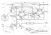
- FIG. 2 an exemplary scheme of a portion of the output block 150 is shown, limitedly to some blocks relevant for the understanding of an embodiment of the present invention.
- a sense amplifier 210 adapted to read the data (logic value) stored in the selected memory cell MC is depicted.
- the example shown and described refers to a so-called “voltage ramp” reading technique, described for example in the already cited European patent application No. 03017939.4 and in the European patent application publication No. EP 1467377, which are incorporated by reference.
- the word line WL of the selected memory cell MC is coupled to a voltage generator block 215 adapted to bias it to a suitable reading voltage Vg which, in case of voltage ramp reading, varies in time, particularly it follows a monotonically increasing trend, for example a linearly increasing trend, for example a voltage ramp.
- Vg a reading voltage
- the reading voltage Vg starting from a very low or substantially zero value (for example, equal to the ground), reaches a final value VgTH in a predetermined time ⁇ t (for example, equal to 10 ns).
- the value of the threshold voltage VgTH is such as to reach the highest threshold voltage of the memory cells MC (corresponding by convention to the logic state 00) when they are programmed.
- the reading voltage Vg is also applied to one (or more) reference cells, only one of which is shown for simplicity, and it is denoted RMC.
- RMC read-only memory
- the selected memory cell MC and the reference cell(s) turns on, and start conducting current, at different times, depending on the respective programming state (that is, as soon as the reading voltage reaches the threshold voltage thereof).
- the currents flowing through the cells are compared by means of corresponding sense amplifiers (in the example at issue, a sense amplifier RSA corresponds to the reference cell RMC) and the timing according to which the selected memory cell MC turns on compared to instants at which the reference cells turn on uniquely identifies the logic value stored in the cell MC.
- the sense amplifier 210 comprises an enable/disenable circuitry comprising, in the example considered, three p-channel MOSFETs P 1 , P 2 and P 3 , the source terminals of which are connected to a common voltage supply line, from which they receive a supply voltage Vdd (for example, 1.8 V).
- the gate terminals of the transistors P 2 and P 3 are coupled (for example, by means of an inverter 295 ) to a control signal line from which they receive a signal SAENABLE_N which is the logic complement of the enabling signal SAENABLE, whereas the gate terminal of the transistor P 1 is connected to an activation signal line and receives an activation signal DATALATCH.
- the sense amplifier 210 also comprises two current generator circuits 220 and 225 connected to the drain terminal of the transistor P 1 .
- the two current generator circuits 220 and 225 respectively comprise pairs of p-channel MOS transistors P 4 , P 5 and P 4 , P 6 connected in a current-mirror circuital configuration.
- the transistors P 4 and P 5 have the source terminal connected to the drain terminal of the transistor P 1 and the gate terminals connected together and further connected to the drain terminal of the transistor P 4 , which is thus connected as a diode.
- the drain terminal of the transistor P 4 is connected to a current generator 230 , which generates a current I 0 .
- the transistor P 6 of the current generator circuit 225 is connected to the transistor P 4 in a current-mirror configuration similar to that of the transistors P 4 and P 5 .
- the drain terminal of the transistor P 5 is coupled (for example, by means of one or more bit line select transistors, not-shown in the drawings, which belong to the column decoder and selector 140 ) to the bit line BL of the selected memory cell MC.
- the drain terminal of the transistor P 2 is connected to a first differential amplifier 235
- the drain terminal of the transistor P 3 is connected to a second differential amplifier 240 .
- the first differential amplifier 235 and the second differential amplifier 240 are amplifiers with a relatively high gain, and each has an inverting input terminal (denoted in FIG. 2 with the symbol “ ⁇ ”) and a non-inverting input terminal (denoted in FIG. 2 with the symbol “+”).
- the inverting terminal of the amplifier 235 is connected to the drain terminal of the transistor P 5 , and thus, in operation, it is coupled to the selected bit line BL; the non-inverting terminal of the amplifier 235 receives a reference voltage VRIF (for example, comprised in a voltage range from 0.5V to 1V) provided by a reference voltage generation circuital block 245 .
- An output terminal of the differential amplifier 235 provides a first output voltage signal OUT 1 and is connected to a non-inverting input terminal of the differential amplifier 240 .
- the inverting input terminal of the differential amplifier 240 is instead connected to the drain terminal of the transistor P 5 , so as to receive a same voltage signal YMS as the inverting input terminal of the amplifier 235 .
- a switch is also connected to the drain terminal of the transistor P 5 , the switch adapted to bring the terminal to ground; for example, an n-channel transistor N 5 has the drain terminal connected to the drain terminal of the transistor P 5 , the source terminal connected to the ground and the gate terminal connected to the activation line DATALATCH.
- the differential amplifier 235 comprises a pair of input n-channel MOSFETs N 1 and N 2 respectively connected to a pair of load p-channel MOSFETs P 7 and P 8 connected in a current-mirror configuration.
- the gate terminals of the transistors N 1 and N 2 are respectively connected to the inverting and the non-inverting input of the differential amplifier 235
- the drain terminals are respectively connected to the drain terminals of the transistors P 7 and P 8 .
- the source terminals of the transistors P 7 and P 8 are instead connected to the drain terminal of the transistor P 2 .
- a current generator 250 for example comprising a n-channel MOSFET with source at ground, is connected to the source terminals of the input transistors N 1 and N 2 .
- the differential amplifier 240 comprises MOSFETs N 3 , N 4 , P 9 and P 10 , and it has a structure similar to that of the differential amplifier 235 ; for this reason it is not described in detail.
- the MOSFETs of the differential amplifiers 235 and 240 are of the so-called “native” type (that is, they are MOSFETs having a low threshold voltage, which is determined only by the level of dopants of the semiconductor well wherein the MOSFET is formed, without any additional dopant implant for modifying the threshold voltage value).
- the native MOSFETs due to their low threshold voltage, have the advantage of being able to conduct current also with low supply voltages, thus reducing the power dissipated during the device operation.
- the differential amplifier 240 has an output terminal which is connected to the drain terminal of the n-channel input transistor N 3 of the non-inverting input terminal.
- the output terminal provides a second output voltage signal OUT 2 , which, differently from the first output voltage signal OUT 1 , is a digital signal, the logic level of which is adapted to provide an indication of the data stored in the selected memory cell MC.
- the drain terminal of the transistor P 6 is connected to a feedback block 255 .
- the feedback block 255 comprises a p-channel MOSFET PR and an n-channel MOSFET NR.
- the transistor NR is a native transistor having a relatively low threshold voltage VTHn (for example, 0.15V) whereas the transistor PR has a higher threshold voltage VTHp (for example, 0.6V).
- the transistor PR has the source terminal connected to the drain terminal of the transistor P 6 , whereas the drain terminal is kept at ground.
- the gate terminal of the transistor PR receives the reference voltage VRIF.
- the transistor NR has the drain terminal connected to the non-inverting input terminal of the differential amplifier 240 , the source terminal connected to the inverting input terminal of the amplifier 235 and the gate terminal connected to the source terminal of the transistor PR.
- the feedback block 255 is coupled to the differential amplifier 235 in such a way to form a negative feedback circuital loop (as disclosed in more detail in the following).
- a combinatory logic circuit is shown, forming a control circuitry 260 adapted for generating the activation signal DATALATCH, in response to the signals PRECH, SAENABLE and OUT 2 .
- the control circuitry 260 comprises a first NOR logic gate 265 connected to a second NOR logic gate 270 .
- the NOR logic gate 265 has two input terminals which receive respectively the second output voltage signal OUT 2 and the control signal PRECH, and has the output terminal connected to one of two inputs of the NOR logic gate 270 .
- the control signal line which brings the logic complement signal SENABLE_N of the enabling signal SAENABLE is coupled to the remaining input of the logic gate 270 .
- the output terminal of the logic gate 270 is connected to the input terminal of an inverter 280 which in output drives the activation signal line DATALATCH.
- a reading operation of the selected memory cell MC is performed in two different phases: a precharging phase of the selected bit line BL, and a reading phase of the data stored in the addressed memory cell MC.
- the address code ADD is received by the memory device, and that such address code ADD identifies (through the respective word line WL and the respective bit line BL) the memory cell MC shown in FIG. 2 .
- the row decoder and selector 130 selects the word line WL to which the memory cell MC belongs by electrically coupling it to the voltage generator block 215
- the column decoder and selector 140 selects the bit line BL to which the memory cell MC belongs, by electrically coupling it (through the select transistors not shown in the drawing) to the sense amplifier 210 .
- the precharging phase starts, in which the control unit 160 asserts the precharging signal PRECH and the enabling signal SAENABLE, bringing them to a high voltage level (that is, the supply voltage Vdd).
- the control circuitry 260 deasserts (bringing it to the logic value 0, typically, the ground) the activation signal DATALATCH.
- the activation signal DATALATCH turns the transistor P 1 on. Indeed, when the precharging signal PRECH is at the high logic level, regardless of the voltage taken by the second output voltage signal line OUT 2 , the output of the logic gate 265 reaches the low logic level. In turn, the output of the logic gate 270 is brought to the high logic level. In such a way, the activation signal DATALATCH is brought to the low logic level, that is, it is deasserted.
- the transistor N 5 is off, and is not able to conduct current.
- the transistors P 1 , P 2 and P 3 are instead on, and their drain terminals are brought to a voltage value approximately equal to the supply voltage Vdd.
- the current generator circuits 220 and 225 deliver two currents I 0 and I 1 (for example, having a value ranging from 6 ⁇ A to 10 ⁇ A).
- the current I 0 is delivered by the transistor P 5 starting from the current generated by the current generator 230 , by mirroring.
- the transistors P 5 and P 4 have a size such that the mirroring ratio is approximately equal to 1, in such a way that the current I 0 delivered by the transistor P 5 has a value equal to the current provided by the current generator 230 .
- the current I 1 is provided by the transistor P 6 , always starting from the current generated by the current generator 230 , by mirroring.
- the transistors of the pair of transistors P 6 and P 4 have size such that the mirroring ratio is approximately equal to 1, so that the current I 1 delivered by the transistor P 6 is equal to the current provided by the current generator 230 .
- the currents I 0 and I 1 are approximately equal.
- the reading voltage Vg takes a substantially zero value.
- the selected memory cell MC is turned off, not being able to conduct any current, and the current I 0 , delivered by the transistor P 5 , flows in the circuital feedback branch and runs through the feedback block 255 .
- the current I 1 delivered by the transistor P 6 flows through the feedback block 255 .
- the current I 0 flows through the transistor NR (and then it continues entering into the output terminal of the differential amplifier 235 ), whereas the current I 1 flows through the transistor PR, and discharges to ground.
- the inverting input of the differential amplifier 235 acts as a “virtual ground”; the higher the gain of the differential amplifier 235 , the closer the voltage YMS to the voltage of the non-inverting terminal of the differential amplifier 235 , and thus to the reference voltage VRIF.
- the control unit 160 deasserts the precharge signal PRECH, bringing its to the low logic level (that is, to ground).
- the precharging phase ends, and the reading phase of the data stored in the selected memory cell MC starts.
- the reading voltage Vg increases, for example linearly, reaching the value VgTH at the instant t 3 .
- the selected memory cell MC is programmed (meaning that the memory cell MC has a relatively high threshold voltage, for example equal to the value VgTH)
- the reading voltage Vg reaches the threshold voltage VgTH of the cell, essentially no current flows through the memory cell MC.
- the current I 0 continues to flow (like in the precharging phase) through the feedback branch and the feedback block 255 , and the second output voltage signal OUT 2 remains at the voltage level at which it was brought during the previous precharging phase (that is, to a value approximately equal to Vdd).
- the reading voltage Vg reaches the value of the threshold voltage VgTH of the memory cell MC, thereby turning the cell on, which can conduct a current Icell.
- the negative feedback established by the feedback loop formed by the differential amplifier 235 and the feedback block 255 keeps the value of the voltage YMS substantially at the reference voltage VRIF (indeed, the inverting input of the differential amplifier 235 acts always as “virtual ground”).
- the transistor NR of the feedback block 255 operates in the triode zone (that is, it does not enter saturation, remaining in the zone of the respective transfer characteristic which has a substantially linear pattern) acting as a feedback resistor.
- the transistor PR is adapted to provide a suitable shifted voltage VRES to the gate terminal of the transistor NR, in order to maintain the latter biased in the triode zone.
- the transistor PR is turned on and the shifted voltage VRES consequently is higher than the reference voltage VRIF of an amount at least equal to the value of the threshold voltage of the transistor PR.
- the shifted voltage can be approximately equal to 1.2 V.
- the transistor NR operates in the triode zone can be explained as follows: if such transistor were to operate in the saturation zone (the zone of the transfer characteristic in which the current is substantially constant irrespective of changes of the drain-to-source voltage), the voltage Vds NR between the transistor drain terminal and source terminal would be higher or at most equal to the voltage drop between the gate terminal and the source terminal thereof, reduced by an amount equal to the transistor threshold voltage.
- the value of the voltage at the gate terminal of the transistor NR is at least equal to the reference voltage VRIF shifted by a value equal to the threshold voltage of the transistor PR, whereas the source voltage of the transistor NR is kept at the value of the reference voltage VRIF by means of the feedback loop comprising the differential amplifier 235 and the feedback block 255 .
- Vds NR VTHp ⁇ VTHn (1) wherein VTHp and VTHn are respectively the threshold voltages of the transistors PR and NR.
- the voltage Vds NR has a value much lower: the variation of the first output voltage signal OUT 1 with respect to the reference voltage VRIF is of the order of ⁇ 100 mV, thus the voltage Vds NR is of the order of 100 mV, much lower than the voltage value Vds NR which it should take for the transistor NR entering in saturation. It follows that the transistor NR operates in the triode zone, and acts substantially as a resistor, from the electrical viewpoint.
- the reading of the data stored in the memory cell MC is performed using a transistor NR operating in triode zone.
- the feedback branch provides the necessary current for supplying the difference between the current Icell of the memory cell MC and the current I 0 provided by the transistor P 5 .
- the first output voltage signal OUT 1 is brought to a voltage value higher than the voltage value taken by the voltage YMS (that is approximately equal to VRIF), and such voltage is applied to the non-inverting input terminal of the differential amplifier 240 , thereby the voltage of the second output voltage signal OUT 2 is brought from the high voltage level (approximately equal to Vdd) to the low voltage level (ground).
- the differential amplifier 240 is thus adapted to sense and amplify the variation of voltage across the transistor NR due to the turning on of the selected memory cell MC.
- the differential amplifier 240 is sensitive to voltage variations of the order of the excursion of the first output voltage signal OUT 1 with respect to the reference voltage VRIF.
- the differential amplifier 240 transforms such voltage variation in a full-swing digital signal—the switching instant thereof from the high level (the supply voltage Vdd) to the low value (ground) provides an indication of the data stored in the memory cell MC (by comparison of the instant at which the second output voltage signal OUT 2 related to the selected cell switches and the instant at which a similar signal OUT 2 R related to the reference cell RMC switches).
- the reading voltage Vg is also applied to one (or more, depending for example on the fact that the cell is bi-level or multi-level) reference cell, and in particular to the reference memory cell RMC.
- the memory cell MC is programmed, and thus has a threshold voltage VgTH higher than that of the reference cell RMC, no current flows through the reference memory cell RMC until the reading voltage Vg reaches the value of the threshold voltage thereof.
- the corresponding sense amplifier RSA brings the second reference output voltage signal OUT 2 R (which is similar to the second output voltage signal OUT 2 ) to the low voltage level (ground).
- the switching occurs at an instant before the instant t 3 at which the second output voltage signal OUT 2 switches, and the timing relation between the two switching instants (that is, between that related to the reference memory cell RMC and that related to the selected memory cell MC) indicates the logic value stored in the selected memory cell MC.
- the cell MC is read as being in a programmed state.
- the control circuitry 260 asserts the activation signal DATALATCH, bringing it to the high logic value (that is, the supply voltage Vdd).
- the transistor P 1 is turned off while the transistor N 5 is turned on, bringing the voltage of the bit line BL of the selected memory cell MC, and thus the voltage YMS, to ground.
- the sense amplifier 210 is disabled and ready for a subsequent reading operation.
- the current Icell when the current Icell is lower than or equal to the current I 0 , the current in excess flows into the feedback branch 255 , and the voltage of the first output voltage signal OUT 1 remains at a voltage value lower than the voltage value taken by the voltage YMS. In such conditions, the voltage of the second output voltage signal OUT 2 is kept at the high level (that is, at a value approximately equal to the supply voltage Vdd).
- the solution according to an embodiment of the present invention significantly reduces the occupation of the integrated circuit area of the output block 150 .
- using the transistors PR and NR in substitution of integrated resistors significantly reduces the area occupied by the sense amplifier 210 in the semiconductor material chip.
- This embodiment is particularly relevant in applications of the memory device in which the reading operations involve a high number of sense amplifiers.
- the integration of the sense amplifier requires a relatively small semiconductor area, this solution is particularly advantageous in memory devices wherein the matrix of cells is divided in a number of partitions, each one comprising one or more sectors.
- the low threshold voltage of the native MOSFET NR causes the latter to operate in the triode zone, thus acting as a resistor placed between the inverting input of the differential amplifier 235 and the output terminal thereof.
- the presence of the negative feedback both during the precharging phase and during the reading phase allows the bit line BL of the memory cell MC not to be left floating, but its voltage is always substantially maintained at the reference potential VRIF, and this reduces or eliminates regions of uncertainty during the operation of the sense amplifier 210 .
- the resistance of the resistor formed by the transistor NR varies with the temperature in way less pronounced than a real integrated resistor. Indeed, from the previous relation (1), it should be noted that the voltage between the drain and source terminals of the transistor NR is almost completely invariant with regard to the temperature, since it depends on the difference between the threshold voltage of the transistors NR and PR.
- the value of the resistor is independent from the reference voltage VRIF, thus allowing setting the voltage value on the drain terminal of the selected memory cell MC in a way which is independent from the desired value for the resistor represented by the transistor NR.
- the memory device has a different structure or comprises equivalent elements (for example, with multilevel memory cells).
- transistor is replaced by two or more transistors which are connected in series and/or in parallel in order to emulate the resistor.
- control circuitry can have a different structure or include equivalent logic gates.
- the memory device 110 of FIG. 1 may compose part of a system, such as a computer system, and be coupled to another component such as a processor or controller.
Landscapes
- Read Only Memory (AREA)
Abstract
Description
Vds NR =VTHp−VTHn (1)
wherein VTHp and VTHn are respectively the threshold voltages of the transistors PR and NR.
Vds NR=0.6V−0.15V=450 mV= Vds NR (2)
Claims (11)
Priority Applications (1)
| Application Number | Priority Date | Filing Date | Title |
|---|---|---|---|
| US12/911,575 US8254194B2 (en) | 2006-02-28 | 2010-10-25 | Sense amplifier with reduced area occupation for semiconductor memories |
Applications Claiming Priority (3)
| Application Number | Priority Date | Filing Date | Title |
|---|---|---|---|
| ITMI2006A000350 | 2006-02-28 | ||
| IT000350A ITMI20060350A1 (en) | 2006-02-28 | 2006-02-28 | READING AMPLIFIER WITH REDUCED AREA EMPLOYMENT FOR SEMICONDUCTOR MEMORIES |
| ITMI2006A0350 | 2006-02-28 |
Related Child Applications (1)
| Application Number | Title | Priority Date | Filing Date |
|---|---|---|---|
| US12/911,575 Division US8254194B2 (en) | 2006-02-28 | 2010-10-25 | Sense amplifier with reduced area occupation for semiconductor memories |
Publications (2)
| Publication Number | Publication Date |
|---|---|
| US20080013381A1 US20080013381A1 (en) | 2008-01-17 |
| US7843738B2 true US7843738B2 (en) | 2010-11-30 |
Family
ID=38949095
Family Applications (2)
| Application Number | Title | Priority Date | Filing Date |
|---|---|---|---|
| US11/713,067 Expired - Fee Related US7843738B2 (en) | 2006-02-28 | 2007-02-28 | Sense amplifier with reduced area occupation for semiconductor memories |
| US12/911,575 Active US8254194B2 (en) | 2006-02-28 | 2010-10-25 | Sense amplifier with reduced area occupation for semiconductor memories |
Family Applications After (1)
| Application Number | Title | Priority Date | Filing Date |
|---|---|---|---|
| US12/911,575 Active US8254194B2 (en) | 2006-02-28 | 2010-10-25 | Sense amplifier with reduced area occupation for semiconductor memories |
Country Status (2)
| Country | Link |
|---|---|
| US (2) | US7843738B2 (en) |
| IT (1) | ITMI20060350A1 (en) |
Families Citing this family (6)
| Publication number | Priority date | Publication date | Assignee | Title |
|---|---|---|---|---|
| ITMI20060536A1 (en) * | 2006-03-23 | 2007-09-24 | St Microelectronics Srl | READING AMPLIFIER WITH REDUCED CURRENT CONSUMPTION FOR SEMICONDUCTOR MEMORIES |
| KR101105434B1 (en) * | 2009-03-02 | 2012-01-17 | 주식회사 하이닉스반도체 | Apparatus and method for evaluating a current sensing characteristic for a semicondoctor memory device |
| CN102185569B (en) * | 2011-04-07 | 2017-07-07 | 北京中星微电子有限公司 | A kind of output-stage circuit of class-D amplifier |
| US8593876B2 (en) | 2011-04-13 | 2013-11-26 | Micron Technology, Inc. | Sensing scheme in a memory device |
| US8994406B2 (en) * | 2011-12-19 | 2015-03-31 | Nanyang Technological University | Digital cell |
| US10762953B2 (en) | 2018-12-13 | 2020-09-01 | International Business Machines Corporation | Memory array with reduced circuitry |
Citations (6)
| Publication number | Priority date | Publication date | Assignee | Title |
|---|---|---|---|---|
| US6625057B2 (en) * | 2000-11-17 | 2003-09-23 | Kabushiki Kaisha Toshiba | Magnetoresistive memory device |
| EP1467377A1 (en) | 2003-04-10 | 2004-10-13 | STMicroelectronics S.r.l. | Method for reading a nonvolatile memory device and corresponding device |
| US20040228162A1 (en) * | 2003-02-18 | 2004-11-18 | Marco Pasotti | Sense amplifier for low-supply-voltage nonvolatile memory cells |
| EP1505605A1 (en) | 2003-08-06 | 2005-02-09 | STMicroelectronics S.r.l. | Improved sensing circuit for a semiconductor memory including bit line precharging and discharging functions |
| US20050063236A1 (en) * | 2003-08-06 | 2005-03-24 | Stmicroelectronics S.R.I | Sense amplifier |
| US20060062042A1 (en) * | 2004-09-23 | 2006-03-23 | Thin Film Electronics Asa | Read method and sensing device |
Family Cites Families (4)
| Publication number | Priority date | Publication date | Assignee | Title |
|---|---|---|---|---|
| US6044019A (en) * | 1998-10-23 | 2000-03-28 | Sandisk Corporation | Non-volatile memory with improved sensing and method therefor |
| US6717449B2 (en) * | 2001-10-23 | 2004-04-06 | Olympus Corporation | Variable resistance circuit and application circuits using the variable resistance circuit |
| US6775178B2 (en) * | 2002-04-04 | 2004-08-10 | Honeywell International Inc. | SEU resistant SRAM using feedback MOSFET |
| JP2004258946A (en) * | 2003-02-26 | 2004-09-16 | Renesas Technology Corp | Memory card |
-
2006
- 2006-02-28 IT IT000350A patent/ITMI20060350A1/en unknown
-
2007
- 2007-02-28 US US11/713,067 patent/US7843738B2/en not_active Expired - Fee Related
-
2010
- 2010-10-25 US US12/911,575 patent/US8254194B2/en active Active
Patent Citations (6)
| Publication number | Priority date | Publication date | Assignee | Title |
|---|---|---|---|---|
| US6625057B2 (en) * | 2000-11-17 | 2003-09-23 | Kabushiki Kaisha Toshiba | Magnetoresistive memory device |
| US20040228162A1 (en) * | 2003-02-18 | 2004-11-18 | Marco Pasotti | Sense amplifier for low-supply-voltage nonvolatile memory cells |
| EP1467377A1 (en) | 2003-04-10 | 2004-10-13 | STMicroelectronics S.r.l. | Method for reading a nonvolatile memory device and corresponding device |
| EP1505605A1 (en) | 2003-08-06 | 2005-02-09 | STMicroelectronics S.r.l. | Improved sensing circuit for a semiconductor memory including bit line precharging and discharging functions |
| US20050063236A1 (en) * | 2003-08-06 | 2005-03-24 | Stmicroelectronics S.R.I | Sense amplifier |
| US20060062042A1 (en) * | 2004-09-23 | 2006-03-23 | Thin Film Electronics Asa | Read method and sensing device |
Also Published As
| Publication number | Publication date |
|---|---|
| ITMI20060350A1 (en) | 2007-09-01 |
| US20110110169A1 (en) | 2011-05-12 |
| US20080013381A1 (en) | 2008-01-17 |
| US8254194B2 (en) | 2012-08-28 |
Similar Documents
| Publication | Publication Date | Title |
|---|---|---|
| US6246621B1 (en) | Semiconductor memory device generating accurate internal reference voltage | |
| US7272059B2 (en) | Sensing circuit for a semiconductor memory | |
| US6788601B2 (en) | Semiconductor memory device and current mirror circuit | |
| US7405988B2 (en) | Method and apparatus for systematic and random variation and mismatch compensation for multilevel flash memory operation | |
| US7082061B2 (en) | Memory array with low power bit line precharge | |
| US20060120175A1 (en) | Memory array with fast bit line precharge | |
| US8830729B2 (en) | Resistive memory apparatus | |
| US6768682B2 (en) | Nonvolatile semiconductor memory and method for controlling programming voltage of nonvolatile semiconductor memory | |
| EP0907955B1 (en) | A multiple bits-per-cell flash shift register page buffer | |
| US8254194B2 (en) | Sense amplifier with reduced area occupation for semiconductor memories | |
| TW200532708A (en) | Apparatus and methods for multi-level sensing in a memory array | |
| US20060126387A1 (en) | Multi-level cell memory device and associated read method | |
| JP2006294213A (en) | Memory device with ramp-like voltage biasing structure based on current generator | |
| KR20010088007A (en) | Word line driver having divided bias line in non-volatile memory device and method thereof | |
| US7072236B2 (en) | Semiconductor memory device with pre-sense circuits and a differential sense amplifier | |
| US7826284B2 (en) | Sense amplifier circuit and method for semiconductor memories with reduced current consumption | |
| US5940322A (en) | Constant voltage generating circuit with improved line voltage control | |
| US7738305B2 (en) | Read-out circuit for or in a ROM memory; ROM memory and method for reading the ROM memory | |
| US8693260B2 (en) | Memory array with two-phase bit line precharge | |
| US6856547B2 (en) | Circuit for biasing an input node of a sense amplifier with a pre-charge stage | |
| US20010050863A1 (en) | Precision programming of nonvolatile memory cells | |
| US6574146B2 (en) | Circuit and method for timing multi-level non-volatile memories | |
| JPH10326495A (en) | Nonvolatile semiconductor memory | |
| JP2007334925A (en) | Nonvolatile semiconductor memory | |
| EP0903754B1 (en) | Nonvolatile semiconductor memory |
Legal Events
| Date | Code | Title | Description |
|---|---|---|---|
| AS | Assignment |
Owner name: STMICROELECTRONICS S.R.L., ITALY Free format text: ASSIGNMENT OF ASSIGNORS INTEREST;ASSIGNORS:GIAMBARTINO, ANTONIO;LA PLACA, MICHELE;MARTINES, IGNAZIO;REEL/FRAME:019901/0344 Effective date: 20070827 |
|
| STCF | Information on status: patent grant |
Free format text: PATENTED CASE |
|
| FPAY | Fee payment |
Year of fee payment: 4 |
|
| MAFP | Maintenance fee payment |
Free format text: PAYMENT OF MAINTENANCE FEE, 8TH YEAR, LARGE ENTITY (ORIGINAL EVENT CODE: M1552) Year of fee payment: 8 |
|
| FEPP | Fee payment procedure |
Free format text: MAINTENANCE FEE REMINDER MAILED (ORIGINAL EVENT CODE: REM.); ENTITY STATUS OF PATENT OWNER: LARGE ENTITY |
|
| LAPS | Lapse for failure to pay maintenance fees |
Free format text: PATENT EXPIRED FOR FAILURE TO PAY MAINTENANCE FEES (ORIGINAL EVENT CODE: EXP.); ENTITY STATUS OF PATENT OWNER: LARGE ENTITY |
|
| STCH | Information on status: patent discontinuation |
Free format text: PATENT EXPIRED DUE TO NONPAYMENT OF MAINTENANCE FEES UNDER 37 CFR 1.362 |
|
| FP | Lapsed due to failure to pay maintenance fee |
Effective date: 20221130 |