US7842620B2 - Method for manufacturing semiconductor device using quadruple-layer laminate - Google Patents
Method for manufacturing semiconductor device using quadruple-layer laminate Download PDFInfo
- Publication number
- US7842620B2 US7842620B2 US12/311,742 US31174207A US7842620B2 US 7842620 B2 US7842620 B2 US 7842620B2 US 31174207 A US31174207 A US 31174207A US 7842620 B2 US7842620 B2 US 7842620B2
- Authority
- US
- United States
- Prior art keywords
- layer
- group
- formula
- film
- polymer
- Prior art date
- Legal status (The legal status is an assumption and is not a legal conclusion. Google has not performed a legal analysis and makes no representation as to the accuracy of the status listed.)
- Active
Links
Classifications
-
- H—ELECTRICITY
- H01—ELECTRIC ELEMENTS
- H01L—SEMICONDUCTOR DEVICES NOT COVERED BY CLASS H10
- H01L21/00—Processes or apparatus adapted for the manufacture or treatment of semiconductor or solid state devices or of parts thereof
- H01L21/02—Manufacture or treatment of semiconductor devices or of parts thereof
- H01L21/027—Making masks on semiconductor bodies for further photolithographic processing not provided for in group H01L21/18 or H01L21/34
- H01L21/033—Making masks on semiconductor bodies for further photolithographic processing not provided for in group H01L21/18 or H01L21/34 comprising inorganic layers
- H01L21/0332—Making masks on semiconductor bodies for further photolithographic processing not provided for in group H01L21/18 or H01L21/34 comprising inorganic layers characterised by their composition, e.g. multilayer masks, materials
-
- G—PHYSICS
- G03—PHOTOGRAPHY; CINEMATOGRAPHY; ANALOGOUS TECHNIQUES USING WAVES OTHER THAN OPTICAL WAVES; ELECTROGRAPHY; HOLOGRAPHY
- G03F—PHOTOMECHANICAL PRODUCTION OF TEXTURED OR PATTERNED SURFACES, e.g. FOR PRINTING, FOR PROCESSING OF SEMICONDUCTOR DEVICES; MATERIALS THEREFOR; ORIGINALS THEREFOR; APPARATUS SPECIALLY ADAPTED THEREFOR
- G03F7/00—Photomechanical, e.g. photolithographic, production of textured or patterned surfaces, e.g. printing surfaces; Materials therefor, e.g. comprising photoresists; Apparatus specially adapted therefor
- G03F7/004—Photosensitive materials
- G03F7/075—Silicon-containing compounds
- G03F7/0752—Silicon-containing compounds in non photosensitive layers or as additives, e.g. for dry lithography
-
- G—PHYSICS
- G03—PHOTOGRAPHY; CINEMATOGRAPHY; ANALOGOUS TECHNIQUES USING WAVES OTHER THAN OPTICAL WAVES; ELECTROGRAPHY; HOLOGRAPHY
- G03F—PHOTOMECHANICAL PRODUCTION OF TEXTURED OR PATTERNED SURFACES, e.g. FOR PRINTING, FOR PROCESSING OF SEMICONDUCTOR DEVICES; MATERIALS THEREFOR; ORIGINALS THEREFOR; APPARATUS SPECIALLY ADAPTED THEREFOR
- G03F7/00—Photomechanical, e.g. photolithographic, production of textured or patterned surfaces, e.g. printing surfaces; Materials therefor, e.g. comprising photoresists; Apparatus specially adapted therefor
- G03F7/004—Photosensitive materials
- G03F7/09—Photosensitive materials characterised by structural details, e.g. supports, auxiliary layers
- G03F7/091—Photosensitive materials characterised by structural details, e.g. supports, auxiliary layers characterised by antireflection means or light filtering or absorbing means, e.g. anti-halation, contrast enhancement
-
- G—PHYSICS
- G03—PHOTOGRAPHY; CINEMATOGRAPHY; ANALOGOUS TECHNIQUES USING WAVES OTHER THAN OPTICAL WAVES; ELECTROGRAPHY; HOLOGRAPHY
- G03F—PHOTOMECHANICAL PRODUCTION OF TEXTURED OR PATTERNED SURFACES, e.g. FOR PRINTING, FOR PROCESSING OF SEMICONDUCTOR DEVICES; MATERIALS THEREFOR; ORIGINALS THEREFOR; APPARATUS SPECIALLY ADAPTED THEREFOR
- G03F7/00—Photomechanical, e.g. photolithographic, production of textured or patterned surfaces, e.g. printing surfaces; Materials therefor, e.g. comprising photoresists; Apparatus specially adapted therefor
- G03F7/004—Photosensitive materials
- G03F7/09—Photosensitive materials characterised by structural details, e.g. supports, auxiliary layers
- G03F7/11—Photosensitive materials characterised by structural details, e.g. supports, auxiliary layers having cover layers or intermediate layers, e.g. subbing layers
-
- G—PHYSICS
- G03—PHOTOGRAPHY; CINEMATOGRAPHY; ANALOGOUS TECHNIQUES USING WAVES OTHER THAN OPTICAL WAVES; ELECTROGRAPHY; HOLOGRAPHY
- G03F—PHOTOMECHANICAL PRODUCTION OF TEXTURED OR PATTERNED SURFACES, e.g. FOR PRINTING, FOR PROCESSING OF SEMICONDUCTOR DEVICES; MATERIALS THEREFOR; ORIGINALS THEREFOR; APPARATUS SPECIALLY ADAPTED THEREFOR
- G03F7/00—Photomechanical, e.g. photolithographic, production of textured or patterned surfaces, e.g. printing surfaces; Materials therefor, e.g. comprising photoresists; Apparatus specially adapted therefor
- G03F7/16—Coating processes; Apparatus therefor
- G03F7/161—Coating processes; Apparatus therefor using a previously coated surface, e.g. by stamping or by transfer lamination
-
- H—ELECTRICITY
- H01—ELECTRIC ELEMENTS
- H01L—SEMICONDUCTOR DEVICES NOT COVERED BY CLASS H10
- H01L21/00—Processes or apparatus adapted for the manufacture or treatment of semiconductor or solid state devices or of parts thereof
- H01L21/02—Manufacture or treatment of semiconductor devices or of parts thereof
- H01L21/027—Making masks on semiconductor bodies for further photolithographic processing not provided for in group H01L21/18 or H01L21/34
- H01L21/0271—Making masks on semiconductor bodies for further photolithographic processing not provided for in group H01L21/18 or H01L21/34 comprising organic layers
- H01L21/0273—Making masks on semiconductor bodies for further photolithographic processing not provided for in group H01L21/18 or H01L21/34 comprising organic layers characterised by the treatment of photoresist layers
- H01L21/0274—Photolithographic processes
- H01L21/0276—Photolithographic processes using an anti-reflective coating
-
- H—ELECTRICITY
- H01—ELECTRIC ELEMENTS
- H01L—SEMICONDUCTOR DEVICES NOT COVERED BY CLASS H10
- H01L21/00—Processes or apparatus adapted for the manufacture or treatment of semiconductor or solid state devices or of parts thereof
- H01L21/02—Manufacture or treatment of semiconductor devices or of parts thereof
- H01L21/04—Manufacture or treatment of semiconductor devices or of parts thereof the devices having at least one potential-jump barrier or surface barrier, e.g. PN junction, depletion layer or carrier concentration layer
- H01L21/18—Manufacture or treatment of semiconductor devices or of parts thereof the devices having at least one potential-jump barrier or surface barrier, e.g. PN junction, depletion layer or carrier concentration layer the devices having semiconductor bodies comprising elements of Group IV of the Periodic System or AIIIBV compounds with or without impurities, e.g. doping materials
- H01L21/30—Treatment of semiconductor bodies using processes or apparatus not provided for in groups H01L21/20 - H01L21/26
- H01L21/31—Treatment of semiconductor bodies using processes or apparatus not provided for in groups H01L21/20 - H01L21/26 to form insulating layers thereon, e.g. for masking or by using photolithographic techniques; After treatment of these layers; Selection of materials for these layers
- H01L21/3105—After-treatment
- H01L21/311—Etching the insulating layers by chemical or physical means
- H01L21/31127—Etching organic layers
- H01L21/31133—Etching organic layers by chemical means
- H01L21/31138—Etching organic layers by chemical means by dry-etching
-
- H—ELECTRICITY
- H01—ELECTRIC ELEMENTS
- H01L—SEMICONDUCTOR DEVICES NOT COVERED BY CLASS H10
- H01L21/00—Processes or apparatus adapted for the manufacture or treatment of semiconductor or solid state devices or of parts thereof
- H01L21/02—Manufacture or treatment of semiconductor devices or of parts thereof
- H01L21/04—Manufacture or treatment of semiconductor devices or of parts thereof the devices having at least one potential-jump barrier or surface barrier, e.g. PN junction, depletion layer or carrier concentration layer
- H01L21/18—Manufacture or treatment of semiconductor devices or of parts thereof the devices having at least one potential-jump barrier or surface barrier, e.g. PN junction, depletion layer or carrier concentration layer the devices having semiconductor bodies comprising elements of Group IV of the Periodic System or AIIIBV compounds with or without impurities, e.g. doping materials
- H01L21/30—Treatment of semiconductor bodies using processes or apparatus not provided for in groups H01L21/20 - H01L21/26
- H01L21/31—Treatment of semiconductor bodies using processes or apparatus not provided for in groups H01L21/20 - H01L21/26 to form insulating layers thereon, e.g. for masking or by using photolithographic techniques; After treatment of these layers; Selection of materials for these layers
- H01L21/3105—After-treatment
- H01L21/311—Etching the insulating layers by chemical or physical means
- H01L21/31144—Etching the insulating layers by chemical or physical means using masks
Definitions
- the present invention relates to a laminate used as an underlayer layer for a photoresist in a lithography process of a semiconductor device and a method for manufacturing a semiconductor device by using the laminate.
- the micro processing is a processing method including forming a thin film of a photoresist on a semiconductor substrate such as silicon wafer, irradiating actinic rays such as ultra violet rays through a mask pattern on which a pattern for a semiconductor device is depicted to develop, and etching the substrate by using an obtained photoresist pattern as a protective film, thereby forming fine unevenness corresponding to the pattern on the surface of the substrate.
- actinic rays such as ultra violet rays
- an acrylic resin type antireflective film having hydroxyl groups as cross-linking reaction groups and light absorption groups in the same molecule for example, an acrylic resin type antireflective film having hydroxyl groups as cross-linking reaction groups and light absorption groups in the same molecule, a novolac resin type antireflective film having hydroxyl groups as cross-linking reaction groups and light absorption groups in the same molecule and the like are included.
- the film has large absorption to light and radiation rays; the film causes no intermixing with a photoresist (insoluble in a photoresist solvent); the film does not cause diffusion of low molecular weight substances from the antireflective film to the upper layer of a photoresist during heating and baking; the film has a higher dry etching rate than that of a photoresist; and the like.
- Patent Document 1 Patent Document 2, Patent Document 3
- a film known as a hard mask containing metal elements such as silicon and titanium has been used as an underlayer film disposed between a semiconductor substrate and a photoresist (see, for example, Patent Document 4, Patent Document 5, Patent Document 6 and Patent Document 7).
- a photoresist and a hard mask have large difference in their constituent components, their removing rates by dry etching significantly depend on a type of gas used in the dry etching.
- the hard mask can be removed by dry etching without significant decrease of the film thickness of the photoresist by selecting an adequate type of gas.
- Patent Document 8 Patent Document 9, Patent Document 10, and Patent Document 11.
- the present invention provides a method for manufacturing a semiconductor device by using a laminate including each layer of an organic foundation layer, a silicon-containing hard mask, an organic antireflective film and a photoresist in this order on a semiconductor substrate.
- a semiconductor substrate is processed by using fine and precise resist patterns in a manner that diffusion of an acid during exposure of the photoresist is eliminated; a focus depth margin of a photoresist is improved; and a shape of a resist pattern is set to rectangle.
- a method for manufacturing a semiconductor device that includes laminating each layer of an organic underlayer film (layer A), a silicon-containing hard mask (layer B), an organic antireflective film (layer C), and a photoresist film (layer D) in this order on a semiconductor substrate;
- a method for manufacturing a semiconductor device that includes forming an organic underlayer film (layer A) on a semiconductor substrate, forming a silicon-containing hard mask (layer B) on the top thereof, forming an organic antireflective film (layer C) on the top thereof, and forming a photoresist film (layer D) on the top thereof, forming a resist pattern in the photoresist film (layer D) by exposure and development, etching the organic antireflective film (layer C) with the resist pattern, etching the silicon-containing hard mask (layer B) with the patterned organic antireflective film (layer C), etching the organic underlayer film (layer A) with the patterned silicon-containing hard mask (layer B), and processing the semiconductor substrate with the patterned organic underlayer film (layer A);
- the organic underlayer film (layer A) has a film thickness of 50 to 500 nm; the silicon-containing hard mask (layer B) has a film thickness of 50 to 200 nm; the organic antireflective film (layer C) has a film thickness of 10 to 100 nm; and a film thickness ratio of layer A:layer B:layer C is a ratio of 1 to 10:1 to 5:1;
- the organic underlayer film (layer A) is a layer including a polymer having an aromatic condensed ring in a main chain or a side chain bonded to the main chain;
- the organic underlayer film (layer A) is a layer including a polymer having a naphthalene ring in a main chain or a side chain bonded to the main chain;
- the silicon-containing hard mask (layer B) has a silicon content of 15 to 45% by mass in the silicon-containing hard mask (layer B);
- the silicon-containing hard mask (layer B) is a layer including a polymer containing a polysilane, a polysiloxane, a polycarbosilane or a combination thereof;
- the silicon-containing hard mask (layer B) is a layer including a polymer containing a polycarbosilane, and a polysilane, a polysiloxane or a combination thereof;
- the organic antireflective film (layer C) includes a polymer in which a molecular structure of the polymer contained in the organic antireflective film (layer C) is similar to a molecular structure of a polymer contained in the photoresist film (layer D);
- the organic antireflective film (layer C) is a layer including a polymer having a benzene ring, a heterocyclic ring or a combination thereof in a main chain constituting the polymer or a side chain bonded to the main chain;
- the heterocyclic ring contained in the polymer of the organic antireflective film (layer C) is a lactone ring
- the organic antireflective film (layer C) includes a polymer having a content ratio of the benzene ring of 30 to 70% by mass.
- a method for manufacturing a semiconductor device including laminating each layer of an organic underlayer film (layer A), a silicon-containing hard mask (layer B), an organic antireflective film (layer C) and a photoresist film (layer D) in this order on a semiconductor substrate, at least four layers described above are laminated.
- a KrF excimer laser wave length: 248 nm
- an ArF excimer laser wave length: 193 nm
- a thickness of the resist layer has become thinner with decrease of the wiring width.
- the dry etching rate of the resist underlayer film is also required to be further enhanced.
- a dry etching gas for example, a fluorine type gas or oxygen gas
- a fluorine type gas or oxygen gas for the organic based resist underlayer film causes decrease of a thickness of the organic based resist film.
- a silicon-containing hard mask layer is used for a foundation layer of an organic based resist film
- the silicon-containing hard mask (layer B) is dry etched with a fluorine type gas
- decrease of a thickness of the organic based resist film resist-pattern formed resist film (layer D)
- the resist pattern according to the thin resist film can be precisely transferred to the silicon-containing hard mask (layer B). Furthermore, when the organic underlayer film (layer A) is dry etched with an oxygen-type dry etching gas, decrease of a thickness of the silicon-containing hard mask (layer B) is small and the resist pattern can be precisely transferred to the organic underlayer film (layer A).
- a semiconductor substrate can be processed with a fluorine type gas by using the organic underlayer film (layer A) to which the resist pattern is transferred.
- a triple-layer laminate formed by laminating an organic underlayer film (layer A), a silicon-containing hard mask (layer B), and a resist film (layer D) in this order on a semiconductor substrate as described above has two problems. One is that adherence between the silicon-containing hard mask (layer B) and the resist film (layer D) thereon is not sufficient. The other problem is that a resist shape is not formed in rectangle, because acid generated from a photoacid generator during exposure of the resist film is diffused into the silicon-containing hard mask (layer B).
- an organic antireflective film (layer C) is disposed between the silicon-containing hard mask (layer B) and the resist film (layer D). That is, the adherence between the organic antireflective film (layer C) and the resist film (layer D) is significantly improved in a manner that the organic antireflective film (layer C) is made to have a chemical structure that is quite similar to the resist film (for example, a polymer of the organic antireflective film (layer C) has benzene rings or lactone rings which are specific for a polymer of the resist film (layer D)), and whereby a focus depth margin during exposure of the resist film can be significantly improved.
- the diffusion of an acid generated from a photoacid generator during exposure of the resist film to the silicon-containing hard mask (layer B) can be prevented in a manner that the organic antireflective film (layer C) is disposed between the silicon-containing hard mask (layer B) and the resist film (layer D).
- a resist pattern can be formed in rectangle.
- the organic antireflective film (layer C) is thinner than the organic underlayer film (layer A) or the silicon-containing hard mask (layer B), the decrease of a thickness of the resist film does not occur when the resist film (layer D) in which the resist pattern is formed is dry etched (for example, a dry etching using a fluorine type gas or oxygen gas), and the resist pattern can be precisely transferred to the organic antireflective film (layer C).
- processing of a semiconductor substrate having a fine wiring width becomes possible by using such a quadruple-layer laminate.
- the present invention includes a method for manufacturing a semiconductor device by using a laminate including each layer of an organic underlayer film (layer A), a silicon-containing hard mask (layer B), an organic antireflective film (layer C) and a photoresist film (layer D) in this order on a semiconductor substrate.
- the organic underlayer film (layer A) used in the present invention is a layer including a polymer having aromatic condensed rings in a main chain or a side chain bonded to the main chain constituting the polymer.
- the aromatic condensed ring includes a naphthalene ring and an anthracene ring.
- This organic underlayer film (layer A) is a layer including a polymer having naphthalene rings in a main chain or a side chain bonded to the main chain. Particularly, a layer including a polymer having naphthalene rings in the side chain bonded to the main chain is preferable.
- the organic underlayer film (layer A) is obtained in a manner that an organic underlayer film (layer A) forming composition including a polymer (a) having naphthalene rings in the side chain bonded to the main chain and a solvent, and as necessary including a cross-linking agent, an acid, an acid generator, a surfactant is applied on a semiconductor substrate and the solvent is removed.
- a solid content in the organic underlayer film (layer A) forming composition is 0.1 to 70% by mass, or 1 to 50% by mass, or 5 to 40% by mass, or 10 to 30% by mass.
- the solid content means components in which the solvent component is removed from the total components of the organic underlayer film (layer A) forming composition.
- the polymer (a) is contained in 10% by mass or more, for example, 30 to 99% by mass, or 50 to 99% by mass, or 65 to 99% by mass.
- the polymer (a) has a weight average molecular weight of 100 to 1000000, preferably 1000 to 200000.
- the polymer (a) is a polymer in which each ratio of a unit structure (number) of the formula (a1) and a unit structure (number) of the formula (a2) to the total unit structures (number) constituting the polymer is 0.02 or more, preferably 0.05 or more,
- R 1 represents a hydrogen atom or a methyl group
- X is a halogen atom, a hydroxyl group, an alkyl group, an alkoxy group, a thiol group, a cyano group, a carboxyl group, an amino group, an amide group, an alkoxycarbonyl group or a thioalkyl group substituted on a naphthalene ring
- n represents an integer of 0 to 7, when n is other than 7, part(s) of the naphthalene ring which is not substituted with X are substituted with hydrogen atom(s)
- R 1 means the same as R 1 defined in the formula (a1), and A 1 is an organic group containing an aromatic hydroxyl group or a hydroxyl group containing ester).
- each ratio of a unit structure (number) of the formula (a1) and a unit structure (number) of the formula (a2) to the total unit structures (number) constituting the polymer is 0.02 or more, preferably 0.05 or more.
- Other monomers can be copolymerized as long as these monomers can be copolymerized with monomers of unit structures of the formula (a1) and the formula (a2). In this case, sum of ratios of each unit structure (number) to the total unit structures (number) constituting the polymer is also 1.00.
- the above-described polymer may be a block copolymer, an alternating copolymer or a random copolymer.
- R 1 represents a hydrogen atom or a methyl group
- X is a halogen atom, a hydroxyl group, an alkyl group, an alkoxy group, a thiol group, a cyano group, a carboxyl group, an amino group, an amide group, an alkoxycarbonyl group or a thioalkyl group substituted on a naphthalene ring
- n represents an integer 0 to 7; when n is other than 7, the remaining part(s) are hydrogen atom(s).
- the unit structure of the formula (a1) is preferably 2-vinyl naphthalene or a condensation product of derivatives of the 2-vinyl naphthalene.
- a fluorine atom, a chlorine atom, a bromine atom and an iodine atom can be used as the halogen atom.
- alkyl groups include alkyl groups having a linear or branched chain and having carbon atom(s) of 1 to 6, and they may be substituted with halogen atoms or the like. For example, a methyl group, an ethyl group, a propyl group, an isopropyl group, a butyl group, a t-butyl group, an n-hexyl group, and a chloromethyl group are included.
- alkoxy groups include alkoxy groups having carbon atom(s) of 1 to 6.
- a methoxy group, an ethoxy group, and an isopropoxy group are included.
- amide groups include amide having carbon atom(s) of 1 to 12.
- a formamide group, an acetamide group, a propionamide group, an isobutylamide group, a benzamide group, a naphthylamide group, and an acrylamide group are included.
- alkoxycarbonyl groups include alkoxycarbonyl groups having carbon atom(s) of 1 to 12.
- a methoxycarbonyl group, an ethoxycarbonyl group, and a benzyloxycarbonyl group are included.
- thioalkyl groups include thioalkyl groups having carbon atom(s) of 1 to 6. For example, a methylthio group, an ethylthio group, a butylthio group, and a hexylthio group are included.
- the unit structure of the formula (a1) in the polymer shows a high etching resistance during processing and the unit structure of the formula (a2) forms a cross-linking bond of hydrogen groups or between a hydrogen group and a cross-linkable compound.
- Selecting ratio of a dry etching rate of the polymer that is smaller compared to a semiconductor substrate can be obtained in a manner that a ratio of the unit structure (number) of the formula (a1) in the total unit structures (number) constituting the polymer is set to 0.4 to 0.98, and a ratio of the unit structure (number) of the formula (a2) in those is set to 0.02 to 0.6. That is, a dry etching resistance is improved.
- R 1 means the same R 1 as defined in the formula (a1), and A 1 is an organic group including an aromatic hydroxyl group or an organic group including a hydroxyl group containing ester.
- a 1 is preferably an organic group including a hydroxyl group containing ester.
- examples of organic groups having an aromatic hydroxyl group include organic groups containing an aromatic ring having 1 to 4 hydroxyl group(s), and examples of the aromatic ring include a benzene ring, a naphthalene ring, an anthracene ring, an imidazole ring, a pyridine ring, and a thiophene ring.
- Examples of organic groups having a hydroxyl group containing ester group include organic groups having a hydroxyl group containing ester generated by the reaction of a carboxyl group containing resin with an aliphatic polyalcohol, an alicyclic polyalcohol, or an aromatic polyalcohol; organic groups having a hydroxyl group containing ester formed by hydrolysis of an epoxy resin obtained by the reaction of a carboxyl group containing resin with epichlorohydrins; and organic groups obtained by further reaction of an aromatic carboxylic acid and an alicyclic carboxylic acid with an epoxy resin obtained by the reaction of a carboxyl group containing resin with epichlorohydrins.
- the unit structure of the formula (a2) is preferably a polymer of 2-hydroxyethyl acrylate or 2-hydroxyethyl methacrylate.
- a polymer in which each ratio of a unit structure (number) of the formula (a1), a unit structure (number) of the formula (a2) and a unit structure (number) of the formula (a3) in the total unit structures (number) constituting the polymer is 0.02 or more can be used as an organic underlayer film (A) forming composition.
- Light absorbance of the underlayer film can be adjusted without significant decrease of a dry etching resistance by introducing the unit structure of the formula (a3):
- R 1 means the same as R 1 defined in the formula (a1)
- B 1 is an organic group including an aliphatic cyclic compound containing ester or an aromatic compound containing ester).
- an organic group including an aliphatic cyclic compound containing ester or an aromatic compound containing ester is, for example, an organic group obtained by the reaction of a carboxyl group containing resin with an alcohol of an aliphatic cyclic compound or an aromatic compound.
- aliphatic cyclic compounds contained in aliphatic cyclic compound containing esters include compounds such as cycloalkanes and cycloalkenes having carbon atoms of 3 to 20, norbornene derivatives, and adamantine derivatives.
- Examples of cycloalkanes include a substituted or unsubstituted cyclopropane, cyclobutane, cyclohexane, and cyclononane.
- Examples of cycloalkenes include a substituted or unsubstituted cyclopropene, cyclobutene, cyclohexene, and cyclonenane.
- Examples of norbornene derivatives include a substituted or unsubstituted norbornene.
- Examples of adamantine derivatives include a substituted or unsubstituted adamantine, diamantine, and triamantine.
- aromatic compounds contained in aromatic compound containing esters include a substituted or unsubstituted benzene ring and anthracene ring.
- substituents in the aromatic compounds include X as defined above, and the substituents X can be substituted up to a maximum substitutionable number in each of a benzene ring, an anthracene ring and the like.
- each ratio of a unit structure (number) of the formula (a1), a unit structure (number) of the formula (a2) and a unit structure (number) of the formula (a3) to the total unit structures (number) constituting the polymer is 0.02 or more, and other monomers can be copolymerized as long as these monomers can be copolymerized with monomers of unit structures of the formula (a1), the formula (a2) and the formula (a3).
- sum of ratios of each unit structure (number) to the total unit structures (number) constituting the polymer is 1.00.
- the above-described polymer may be a block copolymer, an alternating copolymer or a random copolymer.
- a polymer in which the ratios of the unit structure (number) of the formula (a1), the formula (a2) and the formula (a3) to the total unit structures (number) constituting the polymer are set to 0.4 to 0.96, 0.02 to 0.58 and 0.02 to 0.58, respectively, can be formed.
- R 1 means the same as R 1 defined in the formula (a1), and B 1 is an organic group including an aliphatic cyclic compound containing ester or an aromatic compound containing ester.
- the organic group including the aliphatic cyclic compound containing ester or the aromatic compound containing ester is an organic group obtained by the reaction of a carboxyl group containing resin with an alcohol of aliphatic cyclic compound or an aromatic compound.
- a polymer in which each ratio of a unit structure (number) of the formula (a1), a unit structure (number) of the formula (a2) and a unit structure (number) of a formula (a4) in the total unit structures (number) constituting the polymer is 0.02 or more can be used as an organic underlayer film forming composition.
- Light absorbance of an underlayer film can be adjusted without significant decrease of a dry etching resistance by introducing the unit structure of the formula (a4): [Chemical Formula 9] Formula (a4) (where R 1 means the same as R 1 defined in the formula (a1), and B 2 is a substituted or unsubstituted benzene ring or an anthracene ring).
- each ratio of the unit structure (number) of the formula (a1), the unit structure (number) of the formula (a2) and the unit structure (number) of the formula (a4) to the total unit structures (number) constituting the polymer is 0.02 or more, and other monomers can be copolymerized as long as these monomers can be copolymerized with monomers of unit structures of the formula (a1), the formula (a2) and the formula (a4).
- sum of ratios of each unit structure (number) to the total unit structures (number) constituting the polymer is 1.00.
- the above-described polymer may be a block copolymer, an alternating copolymer or a random copolymer.
- a polymer in which the ratios of the unit structure (number) of the formula (a1), the formula (a2), and the formula (a4) to the total unit structures (number) constituting the polymer are set to 0.4 to 0.96, 0.02 to 0.58 and 0.02 to 0.58, respectively, can be formed.
- R 1 means the same R 1 as defined in the formula (a1)
- B 2 is a substituted or unsubstituted benzene ring or an anthracene ring
- substituents in a benzene ring or an anthracene ring include X as described above, and the substituents X can be substituted up to a maximum substitutionable number in each of a benzene ring and an anthracene ring.
- examples of the polymer include a polymer in which a ratio of a unit structure (number) between the formula (a1-1) and the formula (a2-1) in the polymer is 0.9:0.1;
- a polymer in which a ratio of a unit structure (number) between the formula (a1-1), the formula (a2-7) and the formula (a3-6) in the polymer is 0.4:0.2:0.4;
- a polymer in which a ratio of a unit structure (number) between the formula (a1-1), the formula (a2-5) and the formula (a4-1) in the polymer is 0.6:0.2:0.2.
- the organic underlayer film (A) forming composition used in the present invention since the composition is preferably cross-linked by heating after application for the purpose of avoiding intermixing to a silicon-containing hard mask that is overcoated, the organic underlayer film (A) forming composition can further contain a cross-linking agent component.
- the cross-linking agents include a melamine type, a substituted urea type, and a polymer type thereof.
- the cross-linking agents are cross-linking agents having at least two cross-link forming substituents which are compounds such as methoxymethylated glycoluryl, butoxymethylated glycoluryl, methoxymethylated melamine, butoxymethylated melamine, methoxymethylbenzoguanamine, butoxymethylbenzoguanamine, methoxymethylurea, butoxymethylurea, methoxymethylthiourea or butoxymethylthiourea.
- substituents are compounds such as methoxymethylated glycoluryl, butoxymethylated glycoluryl, methoxymethylated melamine, butoxymethylated melamine, methoxymethylbenzoguanamine, butoxymethylbenzoguanamine, methoxymethylurea, butoxymethylurea, methoxymethylthiourea or butoxymethylthiourea.
- condensates of these compounds can also be used.
- the amount to the total solid content is 0.001 to 80% by mass, preferably 0.01 to 50% by mass, and more preferably 0.05 to 40% by mass.
- These cross-linking agents may cause cross-linking reaction due to self-condensation.
- these agents can cause cross-linking reaction with these crosslinkable substituents.
- acidic compounds such as p-toluenesulfonic acid, trifluoromethanesulfonic acid, pyridinium p-toluenesulfonic acid, salicylic acid, sulfosalicylic acid, citric acid, benzoic acid, hydroxybenzoic acid and naphthalene carboxylic acid and/or heat acid generators such as 2,4,4,6-tetrabromocyclohexadienone, benzoin tosylate, 2-nitrobenzyl tosylate and other organic alkyl sulfonate esters can be formulated.
- Formulation amount to the total solid content is 0.0001 to 20% by mass, preferably 0.0005 to 10% by mass.
- Photoacid generators can be added to the organic underlayer film (A) forming composition used in the present invention.
- Examples of preferable photoacid generators include onium salt type photoacid generators such as bis(4-t-butylphenyl)iodonium trifluoromethanesulfonate and triphenylsulfonium trifluoromethanesulfonate, halogen containing compound type photoacid generators such as phenyl-bis(trichloromethyl)-s-triazine, sulfonic acid type photoacid generators such as benzoin tosylate and N-hydroxysuccinimide trifluoromethanesulfonate.
- a content of the photoacid generators to the total solid content is 0.2 to 10% by mass, preferably 0.4 to 5% by mass.
- ethylene glycol monomethyl ether ethylene glycol monoethyl ether, methylcellosolve acetate, ethylcellosolve acetate, diethylene glycol monomethyl ether, diethylene glycol monoethyl ether, propylene glycol, propylene glycol monomethyl ether, propylene glycol monomethyl ether acetate, propylene glycol propyl ether acetate, toluene, xylene, methyl ethyl ketone, cyclopentanone, cyclohexanone, ethyl 2-hydroxypropionate, ethyl 2-hydroxy-2-methylpropionate, ethyl ethoxyacetate, ethyl hydroxyacetate, methyl 2-hydroxy-3-methylbutanoate, methyl 3-methoxypropionate, ethyl 3-methoxypropionate, ethyl 3-methoxypropionate
- high boiling point solvents such as propylene glycol monobutyl ether and propylene glycol monobutyl ether acetate can be used by mixing.
- propylene glycol monomethyl ether, propylene glycol monomethyl ether acetate, ethyl lactate, butyl lactate, cyclohexanone and the like are preferable for improving leveling property.
- a silicon content of the silicon-containing hard mask (layer B) is 15 to 45% by mass.
- a silicon component is derived from a silicon-containing polymer (b).
- a polysilane (b1), a polysiloxane (b2) or a polycarbosilane (b3) can be used singly or in combination thereof.
- This silicon-containing hard mask (layer B) includes a silicon-containing polymer (b) having a polysilane (b1), a polysiloxane (b2), a polycarbosilane (b3) or a combination thereof.
- the silicon-containing hard mask (layer B) can contain a silicon-containing polymer (b) having a polycarbosilane (b3) and a polysilane (b1), a polysiloxane (b2) or a combination thereof.
- the silicon-containing hard mask (layer B) is formed in a manner that a silicon-containing hard mask (layer B) forming composition is applied on an organic underlayer film (layer A) and the solvent therein is removed by drying.
- the silicon-containing hard mask (layer B) forming composition contains the silicon-containing polymer (b), a cross-linking catalyst and a solvent.
- a ratio of the solid content in the silicon-containing hard mask (layer B) forming composition used in the present invention is not particularly limited as long as each component is uniformly dissolved, the content is, for example, 1 to 50% by mass, or 5 to 40% by mass, or 10 to 30% by mass.
- the solid content means components in which the solvent component is removed from the total components of the silicon-containing hard mask (layer B) forming composition.
- a content of the silicon-containing polymer (b) per the solid content is 10% by mass or more, for example, 30% by mass to 99% by mass, or for example, 50% by mass to 99% by mass, or for example, 65% by mass to 99% by mass.
- a mass ratio of a polysilane (b1), a polysiloxane (b2) or a total amount of a combination thereof (b1+b2) to a polycarbosilane (b3) is a ratio of 1 to 10000 parts by mass of (b11+b2) to 100 parts by mass of (b3).
- 1 to 10000 parts by mass of (b2) is formulated relative to 100 parts by mass of (b1).
- the polysilane resin (b11) has a formula (b1-1):
- each R independently represents a hydrogen atom, a hydroxyl group, a cyclic or chain alkyl group having carbon atom(s) of 1 to 10, an alkoxy group having carbon atom(s) of 1 to 10, an aralkyl group having carbon atoms of 7 to 15, an aryl group having carbon atoms of 6 to 14, an aryloxyalkyl group having carbon atoms of 7 to 15, an alkenyl group having carbon atoms of 2 to 10 or an alkoxyalkyl group having carbon atoms of 2 to 10, and m is the number of repeating units and represents 10 to 300), a formula (b1-2):
- each R independently represents a hydrogen atom, a hydroxyl group, a cyclic or chain alkyl group having carbon atom(s) of 1 to 10, an alkoxy group having carbon atom(s) of 1 to 10, an aralkyl group having carbon atoms of 7 to 15, an aryl group having carbon atoms of 6 to 14, an aryloxyalkyl group having carbon atoms of 7 to 15, an alkenyl group having carbon atoms of 2 to 10, an alkoxyalkyl group having carbon atoms of 2 to 10.
- Alkyl groups include a cyclic or chain alkyl group.
- Examples of cyclic alkyl groups having carbon atom(s) of 1 to 10 include cyclopropyl, cyclobutyl, 1-methyl-cyclopropyl, 2-methyl-cyclopropyl, cyclopentyl, 1-methyl-cyclobutyl, 2-methyl-cyclobutyl, 3-methyl-cyclobutyl, 1,2-dimethyl-cyclopropyl, 2,3-dimethyl-cyclopropyl, 1-ethyl-cyclopropyl, 2-ethyl-cyclopropyl, cyclohexyl, 1-methyl-cyclopentyl, 2-methyl-cyclopentyl, 3-methyl-cyclopentyl, 1-ethyl-cyclobutyl, 2-ethyl-cyclobutyl, 3-ethyl-cyclobutyl, 1,2-dimethyl-cyclobutyl, 1,3-dimethyl-cyclobutyl, 2,2-dimethyl-cyclobutyl, 2,3-dimethyl-cyclobut
- Chain alkyl groups having carbon atom(s) of 1 to 10 are alkyl groups having a linear chain or a branched chain and include, for example, methyl, ethyl, n-propyl, i-propyl, n-butyl, i-butyl, s-butyl, t-butyl, n-pentyl, 1-methyl-n-butyl, 2-methyl-n-butyl, 3-methyl-n-butyl, 1,1-dimethyl-n-propyl, 1,2-dimethyl-n-propyl, 2,2-dimethyl-n-propyl, 1-ethyl-n-propyl, n-hexyl, 1-methyl-n-pentyl, 2-methyl-n-pentyl, 3-methyl-n-pentyl, 4-methyl-n-pentyl, 1,1-dimethyl-n-butyl, 1,2-dimethyl-n-butyl, 1,3-dimethyl-
- alkoxy groups having carbon atom(s) of 1 to 10 include methoxy, ethoxy, n-propoxy, i-propoxy, n-butoxy, i-butoxy, s-butoxy, t-butoxy, n-pentoxy, 1-methyl-n-butoxy, 2-methyl-n-butoxy, 3-methyl-n-butoxy, 1,1-dimethyl-n-propoxy, 1,2-dimethyl-n-propoxy, 2,2-dimethyl-n-propoxy, 1-ethyl-n-propoxy, n-hexyloxy, 1-methyl-n-pentyloxy, 2-methyl-n-pentyloxy, 3-methyl-n-pentyloxy, 4-methyl-n-pentyloxy, 1,1-dimethyl-n-butoxy, 1,2-dimethyl-n-butoxy, 1,3-dimethyl-n-butoxy, 2,2-dimethyl-n-butoxy, 2,3-dimethyl-n-butoxy, 3,3-di
- Examples of aralkyl groups having carbon atoms of 7 to 15 include a benzyl group, an o-methylbenzyl group, a m-methylbenzyl group, a p-methylbenzyl group, an o-chlorobenzyl group, a m-chlorobenzyl group, a p-chlorobenzyl group, an o-fluorobenzyl group, a p-fluorobenzyl group, an o-methoxybenzyl group, a p-methoxybenzyl group, a p-nitrobenzyl group, a p-cyanobenzyl group, a phenethyl group, an o-methylphenethyl group, a m-methylphenethyl group, a p-methylphenethyl group, an o-chlorophenethyl group, a m-chlorophenethyl group, a p-chloroph
- aryl groups having carbon atoms of 6 to 14 include a phenyl group, an o-methylphenyl group, a m-methylphenyl group, a p-methylphenyl group, an o-chlorophenyl group, a m-chlorophenyl group, a p-chlorophenyl group, an o-fluorophenyl group, a p-fluorophenyl group, an o-methoxyphenyl group, a p-methoxyphenyl group, a p-nitrophenyl group, a p-cyanophenyl group, an ⁇ -naphthyl group, a ⁇ -naphthyl group, an o-biphenylyl group, a m-biphenylyl group, a p-biphenylyl group, a 1-anthryl group, a 2-anthryl group, a 9-anthryl group
- aryloxyalkyl groups having carbon atoms of 7 to 15 include a phenyloxymethyl group, an o-methyl-phenyloxyethyl group, a m-methyl-phenyloxymethyl group, a p-methyl-phenyloxypropyl group, an o-chlorophenyloxymethyl group, a m-chlorophenyloxyethyl group, a p-chlorophenyloxy isopropyl group, an o-fluorophenyloxyethyl group, a p-fluorophenyloxybutoxy group, an o-methoxyphenyloxy-n-pentyl group, a p-methoxyphenyloxy-t-butyl group, a p-nitrophenyloxymethyl group, a p-cyanophenyloxy-s-butyl group, an ⁇ -naphthyloxymethyl group, a ⁇ -naph
- alkenyl groups having carbon atoms of 2 to 10 include ethenyl, 1-propenyl, 2-propenyl, 1-methyl-1-ethenyl, 1-butenyl, 2-butenyl, 3-butenyl, 2-methyl-1-propenyl, 2-methyl-2-propenyl, 1-ethylethenyl, 1-methyl-1-propenyl, 1-methyl-2-propenyl, 1-pentenyl, 2-pentenyl, 3-pentenyl, 4-pentenyl, 1-n-propylethenyl, 1-methyl-1-butenyl, 1-methyl-2-butenyl, 1-methyl-3-butenyl, 2-ethyl-2-propenyl, 2-methyl-1-butenyl, 2-methyl-2-butenyl, 2-methyl-3-butenyl, 3-methyl-1-butenyl, 3-methyl-2-butenyl, 3-methyl-3-butenyl, 1,1-dimethyl-2-propenyl, 1-i-propylet
- alkoxyalkyl groups having carbon atoms of 2 to 10 include methoxymethyl, ethoxymethyl, n-propoxyethyl, i-propoxymethyl, n-butoxymethyl, i-butoxyethyl, s-butoxymethyl, t-butoxyethyl, n-pentoxy-1-propyl, 1-methyl-n-butoxymethyl, 2-methyl-n-butoxyethyl, 3-methyl-n-butoxyethyl, 1,1-dimethyl-n-propoxymethyl, 1,2-dimethyl-n-propoxyethyl, 2,2-dimethyl-n-propoxyethyl, 1-ethyl-n-propoxy-t-butyl, n-hexyloxymethyl, 1-methyl-n-pentyloxymethyl, 2-methyl-n-pentyloxyethyl, 3-methyl-n-pentyloxypropyl, 4-methyl-n-pentyloxy-s-butyl, 1,
- m is the number of repeating units and represents an integer of 10 to 300.
- a weight average molecular weight of the resin having a structure of the formula (b1-1) is 400 to 12000 or 2000 to 12000.
- R in the resin having a structure of the formula (b1-2), R can be selected from a type of substituents shown in the formula (b1-1).
- m can be selected from the same range as shown in the formula (b1-1).
- Examples of the polysilane resins (b1) include a polymer having a structure of the formula (b1-1), a polymer having a structure of the formula (b1-2) and a polymer having structures of the formula (b1-1) and the formula (b1-2).
- the total of the numbers of repeating units m is 10 to 300, and a weight average molecular weight is 400 to 12000 or 2000 to 12000.
- a ratio of m in the formula (b1-1): m in the formula (b1-2) is preferably 30% to 70%:70% to 30%.
- hydroxy groups exist in both terminals of the resin. These hydroxy groups cause a condensation polymerization reaction by heat baking between the polymers of the formula (b1-1) and (b1-2), or between these polymers and a polysiloxane or a polycarbosilane, so that 3-dimensional cross-linking proceeds. As a result, the product becomes insoluble in a solvent.
- a polysiloxane (b2) is a resin having, for example, structures represented by a formula (b2-1) to a formula (b2-3).
- the polysiloxane (b2) is a resin of the formula (b2-1):
- each R can be selected from a type of the substituents shown in the formula (b1-1).
- m can be selected from the same range as shown in the formula (b1-1).
- Examples of the polysiloxane (b2) include a polymer having a structure of the formula (b2-1), a polymer having a structure of the formula (b2-2), a polymer having a structure of the formula (b2-3), a polymer having structures of the formula (b2-1) and the formula (b2-2), a polymer having structures of the formula (b2-1) and the formula (b2-3), a polymer having structures of the formula (b2-2) and the formula (b2-3), and a polymer having structures of the formula (b2-1), the formula (b2-2) and the formula (b2-3).
- the total of the numbers of repeating units m represents an integer of 10 to 300, and a weight average molecular weight is 400 to 12000 or 2000 to 12000.
- a ratio of mass of the structure of the formula (b2-2) in the entire polysiloxane is preferably 30% by mass or more, and more preferably 40% by mass or more.
- Hydroxy groups exist in both terminals of the polymer having the structures of the formula (b2-1) to the formula (b2-3). These hydroxy groups cause a condensation polymerization reaction by heat baking between the polymers of the formula (b2-1) to (b2-3), or between these resins and a polysilane or a polycarbosilane, so that 3-dimensional cross-linking proceeds. As a result, the product becomes insoluble in a solvent.
- a polycarbosilane resin (b3) is a polymer having, for example, structures represented by a formula (b3-1) and a formula (b3-2).
- the polycarbosilane resin (b3) is a polymer of the formula (b3-1):
- each of R can be selected from a type of the substituents shown in the formula (b1-1).
- m can be selected from the same range as shown in the formula (b1-1).
- the polycarbosilanes (b3) include a polymer having a structure of the formula (b3-1), a polymer having a structure of the formula (b3-2) and a polymer having structures of the formula (b3-1) and the formula (b3-2).
- the total of the numbers of repeating units m represents an integer of 10 to 300, and a weight average molecular weight is 400 to 12000 or 2000 to 12000.
- Hydroxy groups exist in both terminals of the polymer having the structures of the formula (b3-1) and the formula (b3-2). These hydroxy groups cause a condensation polymerization reaction by heat baking between the resins of the formula (b3-1) and the formula (b3-2), or between these resins and a polysilane resin or a polysiloxane resin, so that 3-dimensional cross-linking proceeds. As a result, the product becomes insoluble in a solvent.
- a ratio of mass of the structure of the formula (b3-1) in the entire polycarbosilane is preferably 50% by mass or more, and more preferably 70% by mass or more.
- cross-linking catalysts used in a silicon-containing hard mask (layer B) forming composition for example, proton acids can be used.
- proton acids can be used.
- sulfonic acid compounds such as p-toluenesulfonic acid, trifluoromethanesulfonic acid, pyridinium p-toluenesulfonic acid, sulfosalicylic acid and camphorsulfonic acid, and carboxylic acid compounds such as salicylic acid, citric acid, benzoic acid and hydroxybenzoic acid are included.
- aromatic sulfonic acid compounds can be preferably used.
- aromatic sulfonic acid compounds can include p-toluenesulfonic acid, pyridinium-p-toluenesulfonic acid, sulfosalicylic acid, 4-chlorobenzenesulfonic acid, 4-hydroxybenzenesulfonic acid, benzenedisulfonic acid, 1-naphthalenesulfonic acid, and pyridinium-1-naphthalenesulfonic acid.
- the cross-linking catalysts can be used singly or also in combination of two or more types.
- a content of the cross-linking catalyst per 100 parts by mass of the silicon-containing polymer (b) is 0.1 to 10 parts by mass, or 0.5 to 5 parts by mass, or 1 to 3 part(s) by mass.
- the silicon-containing hard mask (layer B) forming composition can contain a polymer compound, a photoacid generator, a surfactant and the like, as necessary.
- a dry etching rate decrease amount of a film thickness in a unit time
- attenuation coefficient refractive index and the like of a film formed from the silicon-containing hard mask (layer B) forming composition used in the present invention
- Various polymers can be used as the polymer compound without particular limitation.
- a condensation polymerization polymer, an addition polymerization polymer and the like can be used.
- Condensation polymerization polymers and addition polymerization polymers such as polyester, polystyrene, polyimide, an acrylic polymer, a methacrylic polymer, polyvinylether, phenol-novolac, naphthol-novolac, polyether, polyamide and polycarbonate can be used.
- Polymers having structure of aromatic rings, which functions as a light absorption part, such as a benzene ring, a naphthalene ring, an anthracene ring, a triazine ring, a quinoline ring and a quinoxaline ring are preferably used.
- polymer compounds include, for example, addition polymerization polymers containing addition polymerizable monomers as their structure units, such as benzyl acrylate, benzyl methacrylate, phenyl acrylate, naphthyl acrylate, anthryl methacrylate, anthryl methyl methacrylate styrene, hydroxyl styrene, benzylvinylether and N-phenylmaleimide, and condensation polymerization polymers such as phenol-novolac and naphthol-novolac.
- addition polymerization polymers containing addition polymerizable monomers as their structure units, such as benzyl acrylate, benzyl methacrylate, phenyl acrylate, naphthyl acrylate, anthryl methacrylate, anthryl methyl methacrylate styrene, hydroxyl styrene, benzylvinylether and N-phenylmaleimide, and condensation poly
- addition polymerization polymers When addition polymerization polymers are used as the polymer compounds, these polymer compounds may be homopolymers or may be copolymers.
- addition polymerizable monomers are used for manufacture of addition polymerization polymers. Examples of such addition polymerizable monomers include acrylic acid, methacrylic acid, acrylic ester compounds, methacrylic ester compounds, acrylamide compounds, methacrylamide compounds, vinyl compounds, styrene compounds, maleimide compounds, maleic anhydride, and acrylonitrile.
- acrylic ester compounds include methyl acrylate, ethyl acrylate, normalhexyl acrylate, iso-propyl acrylate, cyclohexyl acrylate, benzyl acrylate, phenyl acrylate, anthryl methyl acrylate, 2-hydroxyethyl acrylate, 3-chloro-2-hydroxypropyl acrylate, 2-hydroxypropyl acrylate, 2,2,2-trifluoroethyl acrylate, 2,2,2-trichloroethyl acrylate, 2-bromoethyl acrylate, 4-hydroxybutyl acrylate, 2-methoxyethyl acrylate, tetrahydrofurfuryl acrylate, 2-methyl-2-adamantly-acrylate, 5-acryloyloxy-6-hydroxynorbornene-2-carboxylic-6-lactone, 3-acryloxypropyl triethoxysilane, and glycidyl acrylate.
- methacrylic ester compounds include methyl methacrylate, ethyl methacrylate, normalhexyl methacrylate, isopropyl methacrylate, cyclohexyl methacrylate, benzyl methacrylate, phenyl methacrylate, anthryl methyl methacrylate, 2-hydroxyethyl methacrylate, 2-hydroxypropyl methacrylate, 2,2,2-trifluoroethyl methacrylate, 2,2,2-trichloroethyl methacrylate, 2-bromoethyl methacrylate, 4-hydroxybutyl methacrylate, 2-methoxyethyl methacrylate, tetrahydrofurfuryl methacrylate, 2-methyl-2-adamantyl-methacrylate, 5-methacryloyloxy-6-hydroxynorbornene-2-carboxylic-6-lactone, 3-methacryloxypropyl triethoxysilane, glycidyl
- acrylamide compounds include acrylamide, N-methylacrylamide, N-ethylacrylamide, N-benzylacrylamide, N-phenylacrylamide, N,N-dimethylacrylamide, and N-anthrylacrylamide.
- methacrylamide compounds include methacrylamide, N-methylmethacrylamide, N-ethylmethacrylamide, N-benzylmethacrylamide, N-phenylmethacrylamide, N,N-dimethylmethacrylamide, N-anthrylacrylamide and the like are included.
- vinyl compounds include vinyl alcohol, 2-hydroxyethyl vinyl ether, methyl vinyl ether, ethyl vinyl ether, benzyl vinyl ether, vinyl acetate, vinyltrimethoxysilane, 2-chloroethyl vinyl ether, 2-methoxyethyl vinyl ether, vinylnaphthalene, and vinylanthracene.
- styrene compounds include styrene, hydroxystyrene, chlorostyrene, bromostyrene, methoxystyrene, cyanostyrene, and acetylstyrene.
- maleimide compounds include maleimide, N-methylmaleimide, N-phenylmaleimide, N-cyclohexylmaleimide, N-benzylmaleimide, and N-hydroxyethylmaleimide.
- condensation polymerization polymers examples include, for example, condensation polymerization polymers of glycol compounds and dicarboxylic acid compounds.
- glycol compounds include diethylene glycol, hexamethylene glycol, and butylene glycol.
- dicarboxylic acid compounds include succinic acid, adipic acid, terephthalic acid, and maleic anhydride.
- polyesters, polyamides and polyimides such as polypyromellitimide, poly(p-phenyleneterephthalimide), polybutyleneterephthalate, and polyethyleneterephthalate are included.
- polystyrene poly(4-hydroxy)styrene, polymethyl methacrylate, a copolymer of methyl methacrylate and 4-hydroxystyrene, poly(2-hydroxypropyl) methacrylate, a copolymer of 2-hydroxypropyl methacrylate and anthrylmethyl methacrylate, a copolymer of vinyl ether and methyl vinyl ether, a copolymer of 2-hydroxypropyl methacrylate and benzyl methacrylate, a copolymer of 2-hydroxyethyl acrylate and maleimide, a copolymer of 2-hydroxypropyl methacrylate, styrene and methyl methacrylate, a copolymer of glycidyl methacrylate and 2-hydroxypropyl methacrylate, and a copolymer of styrene and 4-hydroxystyrene.
- hydroxyl groups When hydroxyl groups are contained in the polymer compound, these hydroxyl groups can form cross-linking reaction with the silicon-containing polymer.
- a polymer compound having a weight average molecular weight of, for example, 1000 to 1000000, or 3000 to 300000 or 5000 to 200000, or 10000 to 100000 can be used.
- the polymer compound can be used singly or in combination of two or more types.
- a ratio of the polymer compound per 100 parts by mass of the silicon-containing polymer (b) is 1 to 200 part(s) by mass, or 5 to 100 parts by mass, or 10 to 50 parts by mass, or 20 to 30 parts by mass.
- Photoacid generators generate acids during exposure of photoresist. Accordingly, an acidity of an underlayer film can be adjusted. This is one method for matching the acidity of the underlayer film with the acidity of a photoresist of the upper layer. In addition, a pattern shape of the photoresist formed in the upper layer can be adjusted by adjusting the acidity of the underlayer film.
- Examples of photoacid generators contained in the silicon-containing hard mask (layer B) forming composition according to the present invention include onium salt compounds, sulfonimide compounds, and disulfonyl diazomethane compounds.
- onium salt compounds include iodonium salt compounds such as diphenyliodonium hexafluorophosphate, diphenyliodonium trifluoromethanesulfonate, diphenyliodonium nonafluoro-normalbutanesulfonate, diphenyliodonium perfluoro-normaloctanesulfonate, diphenyliodonium camphorsulfonate, bis(4-tert-butylphenyl)iodonium camphorsulfonate and bis(4-tert-butylphenyl)iodonium trifluoromethanesulfonate, and sulfonium salt compounds such as triphenylsulfonium hexafluoroantimonate, triphenylsulfonium nonafluoro-normalbutanesulfonate, triphenylsulfonium camphorsulfonate and triphenylsulfonium triflu
- sulfonimide compounds include N-(trifluoromethanesulfonyloxy)succinimide, N-(nonafluoro-normalbutanesulfonyloxy)succinimide, N-(camphorsulfonlyoxy)succinimide, and N-(trifluoromethanesulfonyloxy)naphthalimide.
- disulfonyl diazomethane compounds include bis(trifluoromethylsulfonyl)diazomethane, bis(cyclohexylsulfonyl)diazomethane, bis(phenylsulfonyl)diazomethane, bis(p-toluenesulfonyl)diazomethane, bis(2,4-dimethylbenzenesulfonyl)diazomethane, and methylsulfonyl-p-toluenesulfonyldiazomethane.
- Photoacid generators can be used singly or in combination of two or more types.
- a ratio of the photoacid generator per 100 parts by mass of the silicon-containing polymer (b) is 0.01 to 5 parts by mass, or 0.1 to 3 parts by mass, or 0.5 to 1 part(s) by mass.
- any solvents can be used without particular limitation as long as the solvents can dissolve the above-described solid content.
- examples of such solvents can include methylcellosolve acetate, ethylcellosolve acetate, propylene glycol, propylene glycol monomethyl ether, propylene glycol monobutyl ether, propylene glycol monomethyl ether acetate, propylene glycol monoethyl ether acetate, propylene glycol monopropyl ether acetate, propylene glycol monobutyl ether acetate, toluene, xylene, methyl ethyl ketone, cyclopentanone, cyclohexanone, ethyl 2-hydroxylporpionate, ethyl 2-hydroxy-2-methylpropionate, ethyl ethoxyacetate, ethyl hydroxyacetate, methyl 2-
- an organic antireflective film (layer C) containing a polymer that has a molecular structure similar to a molecular structure of a polymer contained in a photoresist film (layer D).
- the organic antireflective film (layer C) used in the present invention includes a polymer having benzene rings, heterocyclic rings or a combination thereof in a main chain or a side chain bonded to the main chain constituting the polymer.
- a polymer having benzene rings, heterocyclic rings or a combination thereof in a side chain bonded to the main chain constituting the polymer is preferable.
- lactone rings or triazine rings is preferably exemplified.
- a content rate of benzene rings in the polymer is preferably 30 to 70% by mass.
- the above-described benzene rings include all benzene rings contained in the polymer, such as benzene rings derived from phenylene and the like contained in the polymer main chain, and benzene rings derived from phenyl groups or phenylene contained in the side chain bonded to the polymer main chain.
- the mass of the benzene rings do not include the mass of substituents bonded to benzene rings.
- the benzene rings do not include naphthalene rings or anthracene rings.
- the organic antireflective film (layer C) is formed in a manner that an organic antireflective film (layer C) forming composition is applied on the upper side of the silicon-containing hard mask (layer B), and a solvent is removed by baking.
- the organic antireflective film (layer C) forming composition is made of a polymer (c), a cross-linking agent and a solvent, and contains a cross-linking catalyst and a surfactant as optional components.
- the solid content of the organic antireflective film (layer C) forming composition is 0.1 to 50% by mass, or 5 to 40% by mass, or 10 to 30% by mass.
- the solid content means components in which the solvent component is removed from the total components of the organic antireflective film (layer C) forming composition.
- a content of the polymer (c) per solid content is 10% by mass or more, for example, 30% by mass to 99% by mass, or for example, 50% by mass to 99% by mass, or for example, 65% by mass to 99% by mass.
- a resin (c1) containing a lactone structure (lactone ring) is preferable for the polymer forming the organic antireflective film (layer C).
- the polymer (c1) is a polymer in which a ⁇ (gamma)-lactone structure forming a five-membered ring structure or a ⁇ (delta)-lactone structure forming a six-membered ring structure being introduced to a main chain or a side chain bonded to the main chain.
- a molecular weight of the polymer (c1) varies depending on an application solvent, a solution viscosity, a film shape and the like to be used, the molecular weight is 1000 to 1000000, preferably 1000 to 200000, and more preferably 1000 to 100000 as a weight average molecular weight.
- ⁇ -lactones used in the above-described polymer (c1) is lactones having a five-membered ring structure, and for example, substituted or unsubstituted lactones, such as ⁇ -butyrolactone, ⁇ -valerolactone, and tetronic acid can be mentioned asn examples.
- ⁇ -lactones is lactones having a six-membered ring structure, and for example, substituted or unsubstituted lactones, such as ⁇ -valerolactone, and ⁇ -caprolactone can be exemplified.
- polymer (c1) for example, resins bonded to a compound having a lactone structure in a side chain bonded to the main chain can be used. These resins have at least a structure unit of a formula (c1-1):
- Q represents a bivalent linking group bonding P and R 1 ;
- R 1 represents a trivalent hydrocarbon group having two carbon atoms to four carbon atoms;
- P represents a bonding group constituting the main chain;
- R 2 represents a hydrogen atom, a methyl group or a halogen atom.
- the trivalent hydrocarbon groups having two carbon atoms to four carbon atoms represented by R 1 constitute lactone rings, and are bonded to P through Q in a portion of these hydrocarbon groups. These hydrocarbon groups may have substituents or may be non-substituted.
- the polymer having the structure of the formula (c1-1) can be produced, for example, in a manner that acrylic type resins such as acrylic acid, halogenated acrylic acid and methacrylic acid are reacted with lactones such as ⁇ -bromo- ⁇ -butyrolactone and ⁇ -bromo- ⁇ -valerolactone.
- a structure of a copolymer (c1-2) having a combination of a structure unit having an acrylic type resin as a main chain and having a ⁇ -lactone or a derivative thereof or a ⁇ -lactone or a derivative thereof in a side chain and a structure unit made of an acrylic resin can be formed.
- a ratio of structure units derived from lactone rings having repeating units (x) is 1 to 76% (x/x+y), and a ratio of structure units corresponding to the acrylic resins having repeating units (y) is 99 to 24% (y/x+y).
- R 2 and R 3 represent a hydrogen atom, a methyl group or a halogen atom, and R 4 represents a hydrogen atom, a substituted or unsubstituted alkyl group having carbon atom(s) of 1 to 10, a substituted or unsubstituted aralkyl group, a substituted or unsubstituted carbon ring type aromatic group, or a substituted or unsubstituted heterocyclic aromatic group.
- examples of preferable alkyl groups having carbon atom(s) of 1 to 10 for R 4 include methyl, ethyl, n-propyl, i-propyl, cyclopropyl, n-butyl, i-butyl, s-butyl, t-butyl, cyclobutyl, 1-methyl-cyclopropyl, 2-methyl-cyclopropyl, n-pentyl, 1-methyl-n-butyl, 2-methyl-n-butyl, 3-methyl-n-butyl, 1,1-dimethyl-n-propyl, 1,2-dimethyl-n-propyl, 2,2-dimethyl-n-propyl, 1-ethyl-n-propyl, cyclopentyl, 1-methyl-cyclobutyl, 2-methyl-cyclobutyl, 3-methyl-cyclobutyl, 1,2-dimethyl-cyclopropyl, 2,3-dimethyl-cyclopropyl, 1-ethyl
- alkyl groups substituted with a hydroxy group such as hydroxyethyl, hydroxypropyl, and hydroxybutyl
- alkyl groups substituted with a halogen atom such as trichloroethyl, and trifluoroethyl
- Examples of preferable aralkyl groups having carbon atoms of 6 to 20 include a benzyl group, an o-methylbenzyl group, a m-methylbenzyl group, a p-methylbenzyl group, an o-chlorobenzyl group, a m-chlorobenzyl group, a p-chlorobenzyl group, an o-fluorobenzyl group, a p-fluorobenzyl group, an o-methoxybenzyl group, a p-methoxybenzyl group, a p-nitrobenzyl group, a p-cyanobenzyl group, a phenethyl group, an o-methylphenethyl group, a m-methylphenethyl group, a p-methylphenethyl group, an o-chlorophenethyl group, a m-chlorophenethyl group, a p-ch
- Examples of preferable carbon ring type aromatic groups having carbon atoms of 6 to 20 include a phenyl group, an o-methylphenyl group, a m-methylphenyl group, a p-methylphenyl group, an o-chlorophenyl group, a m-chlorophenyl group, a p-chlorophenyl group, an o-fluorophenyl group, a p-fluorophenyl group, an o-methoxyphenyl group, a p-methoxyphenyl group, a p-nitrophenyl group, a p-cyanophenyl group, an ⁇ -naphthyl group, a ⁇ -naphthyl group, an o-biphenylyl group, a m-biphenylyl group, a p-biphenylyl group, a 1-anthryl group, a 2-anthryl group, a
- heterocyclic type aromatic groups examples include a 2-thienyl group, a 3-thienyl group, a 2-furyl group, a 3-furyl group, a 2-pyranyl group, a 3-pyranyl group, a 4-pyranyl group, a 2-benzofuranyl group, a 3-benzofuranyl group, a 4-benzofuranyl group, a 5-benzofuranyl group, a 6-benzofuranyl group, a 7-benzofuranyl group, a 1-isobenzofuranyl group, a 4-isobenzofuranyl group, a 5-isobenzofuranyl group, a 2-benzothienyl group, a 3-benzothienyl group, a 4-benzothienyl group, a 5-benzothienyl group, a 6-benzothienyl group, a 7-benzothienyl group, a 1-isobenzothienyl group, a 4-isobenzothienyl
- the resin having the structure of the formula (c1-1) and the resin of the formula (c1-2) may be any of a random copolymer, a block copolymer or a graft copolymer.
- the polymer forming the organic antireflective film (layer C) according to the present invention can be synthesized by methods such as radical polymerization, anion polymerization, and cation polymerization. Various methods such as solution polymerization, suspension polymerization, emulsion polymerization, and bulk polymerization are possible in the polymerization forms.
- the polymer forming the organic antireflective film (layer C) can contain a triazinetrione compound having a hydroxyalkyl structure as a substituent on the nitrogen atom, a triazinetrione oligomer compound having a hydroxyalkyl structure as a substituent on the nitrogen atom or a triazinetrione polymer compound (c2) having a hydroxyalkyl structure as a substituent on the nitrogen atom.
- the organic antireflective film (layer C) forming composition for forming the organic antireflective film (layer C) is made of the triazinetrione compound having a hydroxyalkyl structure as a substituent on the nitrogen atom, the triazinetrione oligomer compound having a hydroxyalkyl structure as a substituent on the nitrogen atom or the triazinetrione polymer compound having a hydroxyalkyl structure as a substituent on the nitrogen atom, and a solvent.
- the composition optionally contains a cross-linking catalyst, surfactant and the like.
- the solid content of the antireflective film forming composition according to the present invention is, for example, 0.1 to 50% by mass, or for example, 0.5 to 30% by mass.
- the solid content means components in which the solvent component is removed from the total components of the antireflective film forming composition.
- a formulation amount of the triazinetrione compound having a hydroxyalkyl structure as a substituent on the nitrogen atom, the triazinetrione oligomer compound having a hydroxyalkyl structure as a substituent on the nitrogen atom or the triazinetrione polymer compound having a hydroxyalkyl structure as a substituent on the nitrogen atom is 10% by mass or more per 100% by mass of the total solid contents, for example, 30% by mass to 99% by mass, for example, 50% by mass to 99% by mass, or further for example, 60% by mass to 95% by mass.
- triazinetrione compounds having a hydroxyalkyl structure as a substituent on the nitrogen atom can include compounds represented by a formula (c2-1).
- each of A 1 , A 2 and A 3 independently represents a hydrogen atom, a methyl group or an ethyl group;
- X represents —OC( ⁇ O)—, —S—, —O— or —NR—, in which R represents a hydrogen atom or a methyl group;
- M represents a benzene ring, a naphthalene ring or an anthracene ring which may be substituted with an alkyl group having carbon atom(s) of 1 to 6, a phenyl group, a naphthyl group, a halogen atom, an alkoxy carbonyl group having carbon atom(s) of 1 to 6, a nitro group, a cyano group, an alkoxy group having carbon atom(s) of 1 to 6 or an alkylthio group having carbon atom(s) of 1 to 6.
- a compound of such a formula (c2-1) can be obtained by, for example, the reaction of a compound represented by a formula (c2-8),
- X represents —OC( ⁇ O)—, —S—, —O— or —NR—, in which R represents a hydrogen atom or a methyl group, and M represents a benzene ring, a naphthalene ring or an anthracene ring which may be substituted with an alkyl group having carbon atom(s) of 1 to 6, a phenyl group, a naphthyl group, a halogen atom, an alkoxy carbonyl group having carbon atom(s) of 1 to 6, a nitro group, a cyano group, an alkoxy group having carbon atom(s) of 1 to 6 or an alkylthio group having carbon atom(s) of 1 to 6.
- Such a reaction of the compound represented by the formula (c2-8) with the compound represented by the formula (c2-15) is preferably preformed in the solution state in which these compounds are dissolved in organic solvents such as benzene, toluene, xylene, ethyl lactate, butyl lactate, propylene glycol monomethyl ether, propylene glycol monomethyl ether acetate, and N-methylpyrrolidone.
- organic solvents such as benzene, toluene, xylene, ethyl lactate, butyl lactate, propylene glycol monomethyl ether, propylene glycol monomethyl ether acetate, and N-methylpyrrolidone.
- organic solvents such as benzene, toluene, xylene, ethyl lactate, butyl lactate, propylene glycol monomethyl ether, propylene glycol monomethyl ether acetate, and N-methylpyrrolidone.
- quaternary ammonium salts such as benzyltriethylammonium chloride, tetrabutylammonium chloride and tetraethylammonium bromide can be used as catalysts of this reaction.
- the reaction time and the reaction temperature of this reaction depend on compounds used, a concentration and the like, they are appropriately selected from the range of the reaction time of 0.1 to 100 hours and the reaction temperature of 20° C. to 200° C.
- a catalyst it can be used in a range of 0.001 to 50% by mass to the total mass of compounds used.
- properties of the antireflective film formed from the antireflective film forming composition significantly depend on a type of the compound of the formula (c2-15) used in the present reaction.
- a type of the compound of the formula (c2-15) used affects a required time for removing the antireflective film formed with the antireflective film forming composition by etching the film.
- a type and the number of the substituents on a benzene ring, a naphthalene ring or an anthracene ring in the compound of the formula (c2-15) affect the required time for removing the antireflective film by etching the film.
- the required time for removing the film by etching can be shortened in a manner that substituents containing hetero atoms such as halogen atoms, nitrogen atoms, oxygen atoms, and sulfur atoms are introduced or the number of the substituents is increased.
- the antireflective film forming composition according to the present invention containing the compound represented by the formula (c2-1) is applied for a process using light having a wavelength of 248 nm (KrF excimer laser), a compound having naphthalene rings or anthracene rings (M is a naphthalene ring or an anthracene ring) as a compound of the formula (c2-15) is preferably used.
- a compound having benzene rings (M is a benzene ring) is preferably used.
- Examples of compounds of the formula (c2-8) used in the reaction in order to obtain the compound of the formula (c2-1) can include tris(2,3-epoxypropyl)-isocyanurate, tris(2-methyl-2,3-epoxypropyl)-isocyanurate, and tris(2,3-epoxybutyl)-isocyanurate.
- Examples of compounds of the formula (c2-15) used in the reaction in order to obtain the compound of the formula (c2-1) can include benzoic acid, monoethyl isophthalate, 2,4-dibromo benzoic acid, 4-methylbenzoic acid, 2-methoxybenzoic acid, 2,3,5-triiodobenzoic acid, 2-chloro-4-nitrobenzoic acid, 4-fluorobenzoic acid, 4-iodobenzoic acid, 4-bromobenzoic acid, 4-t-butylbenzoic acid, 3-trifluoromethylbenzoic acid, 2-nitrobenzoic acid, 4-isopropoxybenzoic acid, 3-cyanobenzoic acid, 3-phenylbenzoic acid, 3-bromo-4-methylbenzoic acid, 2,4,6-tri bromobenzoic acid, 4-methylthiobenzoic acid, and 2-bromo-4-fluorobenzoic acid.
- examples of compounds of the formula (c2-15) can include naphthalene-2-carboxylic acid, 1-bromo-naphthalene-2-carboxylic acid, 4-bromo-3-methoxy-naphthalene-2-carboxylic acid, 3-methyl-naphthalene-2-carboxylic acid, 4-fluoro-naphthalene-1-carboxylic acid, 4-nitro-naphthalene-1-carboxylic acid, 5-bromo-naphthalene-1-carboxylic acid, 8-iodo-naphthalene-1-carboxylic acid, anthracene-9-carboxylic acid, anthracene-2-carboxylic acid, and 10-bromo-anthracene-9-carboxylic acid.
- examples of compounds of the formula (c2-15) can include phenol, 4-methylphenol, 4-chlorophenol, 4-bromophenol, 4-nitrophenol, 2,3,4,5-tetrabromophenol, pentabromophenol, 4-bromo-2-fluorophenol, 4-iodophenol, 2,4,6-triiodophenol, 2,5-dimethyl-4-iodophenol, 4-methylthiophenol, 3-methoxyphenol, 3-bromophenol, 2-cyanophenol, 2,6-diiodo-4-cyanophenol, methyl 3-hydroxybenzoate, 2-naphthol, 1-bromo-2-naphthol, 2-nitro-1-naphthol, 2-methyl-1-naphthol, 4-methoxy-1-naphthol, 2,4-dichloro-1-naphthol, methyl 2-hydroxy-naphthalene-3-carboxylate, 2-hydroxyanthracene, and 9-hydroxy anthracene.
- examples of compounds of the formula (c2-15) can include aniline, 3-chloroaniline, 2-bromoaniline, 4-iodoaniline, 3-methoxyaniline, 3-methylthioaniline, 4-nitroaniline, 3-isopropylaniline, 3,5-dibromoaniline, 2-floro-4-iodoaniline, methyl 2-amino-5-iodobenzoate, 2,4,6-tri-bromoaniline, 4-bromo-3-methylaniline, 2-bromo-4-nitroaniline, 2-bromo-5-trifluoromethylaniline, 3-phenylaniline, 1-aminonaphthalene, 1-amino-4-bromonaphthalene, 1-amino-2-nitronaphthalene, 1-aminoanthracene, and 9-aminoanthracene.
- examples of compounds of the formula (c2-15) can include thiophenol, 2-methylthiophenol, 4-chlorothiophenol, pentachlorothiophenol, 3-methoxythiophenol, 3-bromothiophenol, methyl 2-mercaptobenzoate, 4-nitrothiophenol, 3-iodothiophenol, 1-naphthalenethiol, and 9-mercaptoanthracene.
- compounds reacted with the compounds of the formula (c2-8) in addition to the compounds of the formula (c2-15), for example, compounds having carboxyl groups or hydroxy groups such as 2-thiophene carboxylic acid, 5-bromothiophene carboxylic acid, phenylacetic acid, 4-bromophenoxyacetic acid, benzyl alcohol, 2,4-dibromobenzyl alcohol, 3-bromocinnamic acid, 9-hydroxymethyl anthracene, thiazole-2-carboxylic acid, and 2-amino-5-bromothiazole can also be used.
- carboxyl groups or hydroxy groups such as 2-thiophene carboxylic acid, 5-bromothiophene carboxylic acid, phenylacetic acid, 4-bromophenoxyacetic acid, benzyl alcohol, 2,4-dibromobenzyl alcohol, 3-bromocinnamic acid, 9-hydroxymethyl anthracene, thiazole-2-carboxylic
- Examples of compounds of the formula (c2-1) can include compounds of the following formula (c2-16) (compound number 1 in the following Table 1) and the following formula (c2-17) (compound number 15 in Table 1).
- the compound represented by the formula (c2-1) can be used singly or in combination of two or more types.
- a formulation amount of such compounds of the formula (c2-1) is 10% by mass or more per 100% by mass of the total solid content, for example, 30% by mass to 99% by mass, for example, 50% by mass to 99% by mass, or furthermore, for example, 60% by mass to 95% by mass.
- triazinetrione compounds having a hydroxyalkyl structure as a substituent on the nitrogen atom also include triazinetrione compounds having a substituent represented by a formula (c2-2) as a substituent on the nitrogen atom, and triazinetrione oligomer compounds or triazinetrione polymer compounds having a structure in which at least two triazinetrione ring structures are linked by the linking group represented by a formula (c2-3) through the nitrogen atom.
- each of A 1 , A 2 and A 3 independently represents a hydrogen atom, a methyl group or an ethyl group;
- Y represents a direct bonding or —C( ⁇ O)—;
- Ar represents a benzene ring or a naphthalene ring which may be substituted with an alkyl group having carbon atom(s) of 1 to 6, a phenyl group, a naphthyl group, a halogen atom, an alkoxycarbonyl group having carbon atom(s) of 1 to 6, a nitro group, a carboxyl group, a cyano group, an alkoxy group having carbon atom(s) of 1 to 6, a hydroxy group, a thiol group, an alkylthio group having carbon atom(s) of 1 to 6 or an amino group.
- each of A 1 , A 2 and A 3 independently represents a hydrogen atom, a methyl group or an ethyl group; Y represents a direct bonding or —C( ⁇ O)—; Ar represents a benzene ring or a naphthalene ring which may be substituted with an alkyl group having carbon atom(s) of 1 to 6, a phenyl group, a naphthyl group, a halogen atom, an alkoxycarbonyl group having carbon atom(s) of 1 to 6, a nitro group, a carboxyl group, a cyano group, an alkoxy group having carbon atom(s) of 1 to 6, a hydroxy group, a thiol group, an alkylthio group having carbon atom(s) of 1 to 6 or an amino group.
- the compound of the formula (c2-4) can be obtained in a manner that a triazinetrione compound having substituents on the nitrogen atom represented by a formula (c2-6):
- a 1 , A 2 and A 3 independently represents a hydrogen group, a methyl group or an ethyl group
- the compound represented by the formula (c2-7) can be used singly, the compounds can also be used in combination of two or more types.
- This reaction is preferably performed in the solution state in which these compounds are dissolved in organic solvents such as benzene, toluene, xylene, ethyl lactate, butyl lactate, propylene glycol monomethyl ether, propylene glycol monomethyl ether acetate, and N-methylpyrrolidone.
- organic solvents such as benzene, toluene, xylene, ethyl lactate, butyl lactate, propylene glycol monomethyl ether, propylene glycol monomethyl ether acetate, and N-methylpyrrolidone.
- quaternary ammonium salts such as benzyltriethylammonium chloride, tetrabutylammonium chloride, tetraethylammonium bromide can be used as catalysts of this reaction.
- reaction time and the reaction temperature of this reaction depend on compounds, a concentration and the like to be used, they are appropriately selected from the range of the reaction time of 0.1 to 100 hours and the reaction temperature of 20° C. to 200° C.
- a catalyst When a catalyst is used, it can be used in a range of 0.001 to 50% by mass to the total mass of compounds used.
- the triazinetrione compound having two or three nitrogen atoms having substituents represented by the formula (c2-6) When the triazinetrione compound having two or three nitrogen atoms having substituents represented by the formula (c2-6) is used, the case that all of the substituents are reacted with the compounds of the formula (c2-7), or the case that only one or two substituent(s) in these groups are reacted with the compounds of the formula (c2-7) can be considered.
- the triazinetrione compounds used in the antireflective film forming composition according to the present invention include both cases.
- the compound obtained in a manner that all of the substituents in the compound of the formula (c2-8) having three substituents of the formula (c2-6) are reacted with the compound of the formula (c2-7), is preferably used, so that the compound represented by a formula (c2-18) is preferably used (in the formula (c2-18),
- Y represents a direct bonding or —C( ⁇ O)—;
- Ar represents a benzene ring or a naphthalene ring which may be substituted with an alkyl group having carbon atom(s) of 1 to 6, a phenyl group, a naphthyl group, a halogen atom, an alkoxycarbonyl group having carbon atom(s) of 1 to 6, a nitro group, a carboxyl group, a cyano group, an alkoxy group having carbon atom(s) of 1 to 6, a hydroxy group, a thiol group, an alkyl group having carbon atom(s) of
- Examples of compounds of the formula (c2-7) used for the reaction with triazinetrione compounds having substituents represented by the formula (c2-6) on the nitrogen atoms can include the compounds represented by formulae (c2-9) to (c2-14):
- B represents a hydrogen atom, an alkyl group having carbon atom(s) of 1 to 6, a phenyl group, a naphthyl group, a halogen atom, an alkoxycarbonyl group having carbon atom(s) of 1 to 6, a nitro group, a carboxyl group, a cyano group, an alkoxy group having carbon atom(s) of 1 to 6, a hydroxy group, a thiol group, an alkylthio group having carbon atom(s) of 1 to 6 or an amino group; n represents the number of 1 to 6; m represents the number of 1 to 4, and when n and m are 2 or more, B may be the same or different).
- the compounds of the formulae (c2-9) to (c2-14) can be used singly, the compounds can also be used in combination of two or more types.
- triazinetrione oligomer compounds or triazinetrione polymer compounds in which at least two of the above-described triazinetrione ring structure have a linked structure through the nitrogen atoms with the linking group represented by the formula (c2-3) triazinetrione oligomer compounds or triazinetrione polymer compounds having structures represented by the formula (c2-5) can be used:
- each of A 1 , A 2 and A 3 independently represents a hydrogen atom, a methyl group or an ethyl group; Y represents a direct bonding or —C( ⁇ O)—; Ar represents a benzene ring or a naphthalene ring which may be substituted with an alkyl group having carbon atom(s) of 1 to 6, a phenyl group, a naphthyl group, a halogen atom, an alkoxycarbonyl group having carbon atom(s) of 1 to 6, a nitro group, a carboxyl group, a cyano group, an alkoxy group having carbon atom(s) of 1 to 6, a hydroxy group, a thiol group, an alkylthio group having carbon atom(s) of 1 to 6 or an amino group.
- a molecular weight of the triazinetrione oligomer compounds or the triazinetrione polymer compounds having structures represented by the formula (c2-5) is not particularly limited, weight average molecular weights thereof are, for example, 700 to 200000, or for example 1000 to 50000.
- the triazinetrione oligomer compounds or the triazinetrione polymer compounds having structures represented by the formula (c2-5) can be obtained in a manner that the triazinetrione compound having two or three nitrogen atoms having substituents represented by the formula (c2-6) on the nitrogen atoms is reacted with an aromatic compound represented by the formula (c2-7).
- the compound represented by the formula (c2-7) can be used singly, the compounds can also be used in combination of two or more types.
- triazinetrione compounds having two or three nitrogen atoms having substituents represented by the formula (c2-6) on the nitrogen atoms can be used singly, the compounds can also be used in combination thereof.
- the compound having three substituents of the formula (c2-6), that is, the compound represented by the formula (c2-8) is preferably used.
- the case that one or two substituent(s) of the formula (c2-6) in the triazine compounds which is raw materials for the production of these oligomer compounds or polymer compounds participates in formation of the linking group of the formula (c2-3), that is, in the formation of the oligomer structure or the polymer structure, and the remaining substituents of the formula (c2-6) is not reacted or participates in formation of the substituent of the formula (c2-2) is considered.
- the case that all (that is, two or three) substituents of the formula (c2-6) participates in formation of the linking group of the formula (c2-3), that is, in the formation of the oligomer structure or the polymer structure is also considered.
- the compound of the formula (c2-8) which is the compound having three substituents of the formula (c2-6) is preferably used, and particularly the compound of a formula (c2-19) is preferably used (in which A 4 represents a hydrogen atom or alkyl group).
- the compound having a naphthalene ring or the compound having a benzene ring represented by the formulae (c2-9) to (c2-14) can be included. Although these compounds can be used singly, these compounds can also be used in combination of two or more types.
- the triazinetrione compounds, the triazinetrione oligomer compounds and the triazinetrione polymer compounds obtained by the reaction of a triazinetrione compound having substituents represented by the formula (c2-6) on the nitrogen atoms with the phenyl compound or the naphthalene compound represented by the formula (c2-7) are included.
- the antireflection film forming composition according to the present invention contains any composition of a composition only containing such a triazinetrione compound, a composition only containing a triazinetrione oligomer compound and a composition only containing a triazinetrione polymer compound.
- any compositions of a composition made of a mixture of such a triazinetrione compound and a triazinetrione oligomer compound, a composition made of a mixture of such a triazinetrione compound and a triazinetrione polymer compound, a composition made of a mixture of such a triazinetrione oligomer compound and a triazinetrione polymer compound, and a composition made of a mixture of such a triazinetrione compound, a triazinetrione oligomer compound and a triazinetrione polymer compound are contained.
- a polymer forming the organic antireflective film (layer C) contains a polymer having a structure represented by a formula (c3-1).
- the polymer having a structure represented by the formula (c3-1) is an essential component.
- a ratio of the polymer having a structure represented by the formula (c3-1) in the solid content in the antireflection film forming composition is 50% by mass or more, preferably 60% by mass or more, from a viewpoint of an antireflection effect.
- a ratio of the solid content in the antireflection film forming composition is not particularly limited as long as each component is uniformly dissolved in a solvent, the ratio is, for example, 0.5 to 50% by mass, or 1 to 30% by mass, or 5 to 25% by mass.
- the solid content means components in which the solvent component is removed from the total components of the antireflective film forming composition.
- each of A 1 , A 2 , A 3 , A 4 , A 5 and A 6 independently represents a hydrogen, a methyl group or an ethyl group.
- X 1 represents a formula (c3-2), a formula (c3-3) or a formula (c3-4).
- Q represents a formula (c3-5) or a formula (c3-6).
- each of R 1 and R 2 independently represent a hydrogen atom, an alkyl group having carbon atom(s) of 1 to 6, an alkenyl group having carbon atoms of 3 to 6, a benzyl group or a phenyl group.
- the alkyl groups include a methyl group, an ethyl group, an isopropyl group, a normalbutyl group, and a cyclohexyl group.
- Specific examples of the alkenyl groups include a 2-propenyl group and a 3-butenyl group.
- the phenyl group may be substituted with a group selected from a group consisting of an alkyl group having carbon atom(s) of 1 to 6, a halogen atom, an alkoxy group having carbon atom(s) of 1 to 6, a nitro group, a cyano group, a hydroxy group, and an alkylthio group having carbon atom(s) of 1 to 6.
- R 1 and R 2 may be bonded to each other to form a ring having carbon atoms of 3 to 6.
- Such rings include a cyclobutane ring, a cyclopentane ring and a cyclohexane ring.
- R 3 represents an alkyl group having carbon atom(s) of 1 to 6, an alkenyl group having carbon atoms of 3 to 6, a benzyl group or a phenyl group.
- the phenyl group may be substituted with a group selected from a group consisting of an alkyl group having carbon atom(s) of 1 to 6, a halogen atom, an alkoxy group having carbon atom(s) of 1 to 6, a nitro group, a cyano group, a hydroxy group, and an alkylthio group having carbon atom(s) of 1 to 6.
- Specific examples of the alkyl groups and alkenyl groups include the same group as described above.
- Q 1 represents an alkylene group having carbon atom(s) of 1 to 10, a phenylene group, a naphthylene group or an anthrylene group.
- Each of the phenylene group, the naphthylene group and the anthrylene group may be substituted with a group selected from a group consisting of an alkyl group having carbon atom(s) of 1 to 6, a halogen atom, an alkoxy group having carbon atom(s) of 1 to 6, a nitro group, a cyano group, a hydroxy group, and an alkylthio group having carbon atom(s) of 1 to 6.
- Specific examples of the alkylene groups include a methylene group, an ethylene group, a propylene group, a normalpentylene group, a cyclohexylene group, and a 2-methylpropylene group.
- n 1 and n 2 represents the number of 0 or 1
- X 2 represents the formula (c3-2) or the formula (c3-3).
- the polymer having a structure represented by the formula (c3-1) can be produced by the reaction of a compound represented by a formula (c3-7) with a compound represented by a formula (c3-8).
- the reaction of the compound represented by the formula (c3-7) with the compound represented by the formula (c3-8) is preferably preformed in the solution state in which these compounds are dissolved in organic solvents such as benzene, toluene, xylene, ethyl lactate, butyl lactate, propylene glycol monomethyl ether, propylene glycol monomethyl ether acetate, and N-methylpyrrolidone.
- organic solvents such as benzene, toluene, xylene, ethyl lactate, butyl lactate, propylene glycol monomethyl ether, propylene glycol monomethyl ether acetate, and N-methylpyrrolidone.
- quaternary ammonium salts such as benzyltriethylammonium chloride, tetrabutylammonium chloride and tetraethylammonium bromide can be used as catalysts.
- reaction time and the reaction temperature of this reaction depend on compounds, a concentration and the like to be used, they are appropriately selected from the range of the reaction time of 0.1 to 100 hours and the reaction temperature of 20° C. to 200° C.
- the catalyst When the catalyst is used, it can be used in a range of 0.001 to 30% by mass to the total mass of compounds used.
- a ratio of the compound represented by the formula (c3-7) and the formula (c3-8) used for the reaction is, in molar ratio, 3:1 to 1:3 and preferably 3:2 to 2:3 as the compound represented by the formula (c3-7): the compound represented by the formula (c3-8).
- each two reaction sites (N—H sites) in the compound of the formula (c3-7) causes an epoxy ring opening reaction with the epoxy ring portions in different compounds of the formula (c3-8).
- the polymer having a structure represented by the formula (c3-1) is produced. It is considered that the polymer is made of repeating structures represented by the formula (c3-1).
- hydantoin compounds such as hydantoin, 5,5-diphenylhydantoin, 5,5-dimethylhydantoin, 5-ethylhydantoin, 5-benzylhydantoin, 5-ethyl-5-phenylhydantoin, 5-methylhydantoin, 5,5-tetramethylenehydantoin, 5,5-pentamethylenehydantoin, 5-(4-hydroxybenzyl)hydantoin, 5-phenylhydantoin, 5-hydroxymethylhydantoin and 5-(2-cyanoethyl)hydantoin.
- hydantoin compounds such as hydantoin, 5,5-diphenylhydantoin, 5,5-dimethylhydantoin, 5-ethylhydantoin, 5-benzylhydantoin, 5-ethyl-5-phenylhydantoin, 5-methylhydantoin, 5,5-
- specific examples of the compound represented by the formula (c3-7) include barbituric acid compounds such as 5,5-diethylbarbituric acid, 5,5-diallylmalonylurea, 5-ethyl-5-isoarnylbarbituric acid, 5-allyl-5-isobutylbarbituric acid, 5-allyl-5-isopropylbarbituric acid, 5-p-bromoallyl-5-sec-butylbarbituric acid, 5-ethyl-5-(1-methyl-1-butenyl)barbituric acid, 5-isopropyl-5- ⁇ -bromoallylbarbituric acid, 5-(1-cyclohexyl)-5-ethylmalonylurea, 5-ethyl-5-(1-methyl butyl) malonylurea, 5,5-dibromobarbituric acid, 5-phenyl-5-ethylbarbituric acid and 5-ethyl-5-normalbuty
- specific examples of the compound represented by the formula (c3-7) include isocyanuric acid compounds such as monoallylisocyanuric acid, monomethylisocyanuric acid, monopropylisocyanuric acid, monoisopropylisocyanuric acid, monophenylisocyanuric acid, monobenzylisocyanuric acid, monochloroisocyanuric acid and monoethylisocyanuric acid.
- Specific examples of the compound represented by the formula (c3-8) used for producing the polymer having the structure represented by the formula (c3-1) include diglycidyl compounds such as diglycidyl terephthalate, diglycidyl isophthalate, diglycidyl phthalate, diglycidyl 2,5-dimethylterephthalate, diglycidyl 2,5-diethylterephthalate, diglycidyl 2,3,5,6-tetrachloroterephthalate, diglycidyl 2,3,5,6-tetrabromoterephthalate, diglycidyl 2-nitroterephthalate, diglycidyl 2,3,5,6-tetrafluoroterephthalate, diglycidyl 2,5-dihydroxyterephthalate, diglycidyl 2,6-dimethylterephthalate, diglycidyl 2,5-dichloroterephthalate, diglycidyl 2,3-dichloroisophthalate, diglycidyl 3-nitroisophthalate
- specific examples of the compound represented by the formula (c3-8) include diglycidylhydantoin compounds such as 1,3-diglycidylhydantoin, 1,3-diglycidyl-5,5-diphenylhydantoin, 1,3-diglycidyl-5,5-dimethylhydantoin, 1,3-diglycidyl-5-methylhydantoin, 1,3-diglycidyl-5-ethyl-5-phenylhydantoin, 1,3-diglycidyl-5-benzylhydantoin, 1,3-diglycidyl-5-hydantoin acetic acid, 1,3-diglycidyl-5-ethyl-5-methylhydantoin, 1,3-diglycidyl-5-methylhydantoin, 1,3-diglycidyl-5,5-tetramethylenehydantoin, 1,3-diglycidyl-5,5-pentamethylenehydantoin, 1, 1,3
- specific examples of the compound represented by the formula (c3-8) include diglycidylbarbituric acid compounds such as 1,3-diglycidyl-5,5-diethylbarbituric acid, 1,3-diglycidyl-5-phenyl-5-ethylbarbituric acid, 1,3-diglycidyl-5-ethyl-5-isoamylbarbituric acid, 1,3-diglycidyl-5-allyl-5-isobutylbarbituric acid, 1,3-diglycidyl-5-allyl-5-isopropylbarbituric acid, 1,3-diglycidyl-5- ⁇ -bromoallyl-5-sec-butylbarbituric acid, 1,3-diglycidyl-5-ethyl-5-(1-methyl-1-butenyl)barbituric acid, 1,3-diglycidyl-5-isopropyl-5-O-bromoallylbarbituric acid, 1,3-diglycidyl-5
- the obtained polymer is a polymer made of the structure of the formula (c3-15).
- 5,5-diethylbarbituric acid is used as the compound of the formula (c3-7)
- diglycidyl terephthalate and ethylene glycol diglycidyl ether are used as the two types of the compounds of the formula (c3-8)
- the obtained polymer is a polymer made of the structure of the formula (c3-16) and the structure of the formula (c3-27).
- the polymer having the structure represented by the formula (c3-1) can be produced by the reaction of a compound represented by a formula (c3-9) with a compound represented by a formula (c3-10).
- reaction of the compound represented by the formula (c3-9) and the formula (c3-10) can be performed in a similar condition to the reaction of the compound represented by the formula (c3-7) and the formula (c3-8).
- a ratio of the compound represented by the formula (c3-9) and the formula (c3-10) used for the reaction is, in molar ratio, 3:1 to 1:3 and preferably 3:2 to 2:3 as the formula (c3-9): the formula (c3-10).
- each of two reaction sites (N—H sites or O—H sites) in the compound of the formula (c3-10) causes an epoxy ring opening reaction with the epoxy ring portions in different compounds of the formula (c3-9).
- a polymer having a structure represented by the formula (c3-1) is produced. It is considered that the polymer is made of the repeating structures represented by the formula (c3-1).
- Specific examples of the compounds represented by the formula (c3-9) which are used for producing the polymer having the structure represented by the formula (c3-1) include the diglycidylhydantoin compounds and the diglycidylbarbituric acid compounds in the specific examples of the formula (c3-8).
- diglycidylisocyanuric acid compounds such as monoallyldiglycidylisocyanuric acid, monoethyldiglycidylisocyanuric acid, monopropyldiglycidylisocyanuric acid, monoisopropyldiglycidylisocyanuric acid, monophenyldiglycidylisocyanuric acid, monobromodiglycidylisocyanuric acid and monomethyldiglycidylisocyanuric acid can further be included.
- Specific examples of the compounds represented by the formula (c3-10) which are used for producing the polymer having the structure represented by the formula (c3-1) can include the hydantoin compounds and the barbituric acid compounds in the specific examples of the formula (c3-7).
- terephthalic acid isophthalic acid, phthalic acid, 2,5-dimethylterephthalic acid, 2,5-diethylterephthalic acid, 2,3,5,6-tetrachloroterephthalic acid, 2,3,5,6-tetrabromoterephthalic acid, 2-nitroterephthalic acid, 2,3,5,6-tetrafluoroterephthalic acid, 2,5-dihydroxyterephthalic acid, 2,6-dimethylterephthalic acid, 2,5-dichloroterephthalic acid, 2,3-dichloroisophthalic acid, 3-nitroisophthalic acid, 2-bromoisophthalic acid, 2-hydroxyisophthalic acid, 3-hydroxyisophthalic acid, 2-methoxyisophthalic acid, 5-phenylisophthalic acid, 3-nitrophthalic acid, 3,4,5,6-tetrachlorophthalic acid, 4,5-dichlorophthalic acid, 4-hydroxyphthalic acid, 4-nitrophthalic acid, 4-methyl
- the compound in the production of the polymer having a structure represented by the formula (c3-1), although each compound represented by the formula (c3-9) and the formula (c3-10) can be used singly, the compound can also be used in combination of two or more types.
- the obtained polymer is a polymer made of the structure of the formula (c3-13).
- the obtained polymer is a polymer made of the structures of the formula (c3-13) and the structures of the formula (c3-24).
- polymers can be used singly or in combination of two or more types.
- a molecular weight of the polymer having the structure represented by the formula (c3-1) contained in the antireflection film forming composition according to the present invention is, for example, 1000 to 200000, or for example 3000 to 100000, or 5000 to 20000 as a weight average molecular weight.
- the polymer forming the organic antireflective film (layer C) contains a polymer having the repeating unit structures represented by a formula (c4-1) or a formula (c4-2).
- a ratio of the polymer having the repeating unit structures represented by the formula (c4-1) or the formula (c4-2) in the solid content of the antireflection film forming composition is, from a viewpoint of antireflection effect, 50% by mass or more, preferably 60% by mass or more, for example 50 to 100% by mass, or 60 to 99% by mass, or 70 to 95% by mass.
- a ratio of the solid content in the antireflection film forming composition according to the present invention is not particularly limited as long as each component is uniformly dissolved in a solvent, the ratio is, for example, 1 to 50% by mass, or 5 to 30% by mass, or 10 to 25% by mass.
- the solid content means components in which the solvent component is removed from the total components of the antireflective film forming composition for lithography.
- each of R 1 and R 2 independently represents a hydrogen atom, a methyl group, an ethyl group or a halogen atom; each of A 1 , A 2 , A 3 , A 4 , A 5 and A 6 independently represents a hydrogen atom, a methyl group or an ethyl group; Q represents the formula (c4-3) or the formula (c4-4).
- the halogen atom is a fluorine atom, a chlorine atom, a bromine atom or an iodine atom.
- Q 1 represents an alkylene group having carbon atom(s) of 1 to 15, a phenylene group, a naphthylene group or an anthrylene group.
- Each of the phenylene group, the naphthylene group and the anthrylene group may be substituted with a group selected from a group consisting of an alkyl group having carbon atom(s) of 1 to 6, a halogen atom, an alkoxy group having carbon atom(s) of 1 to 6, a nitro group, a cyano group, a hydroxy group, and an alkylthio group having carbon atom(s) of 1 to 6.
- alkyl groups include a methyl group, an ethyl group, an isopropyl group, a normalbutyl group, and a cyclohexyl group.
- alkoxy groups include a methoxy group, an ethoxy group, a normalpentyloxy group, an isopropoxy group, and a cyclohexyloxy group.
- alkylthio groups include a methylthio group, an ethylthio group, a normalpentylthio group, an isopropylthio group, and a cyclohexylthio group.
- the halogen atom is a fluorine atom, a chlorine atom, a bromine atom or an iodine atom.
- alkylene groups include linear alkylene groups such as a methylene group, an ethylene group, a normalpropylene group, a normalpentylene group and a normaloctylene group; branched alkylene groups such as a 2-methylpropylene group, and a 1,4-dimethylbutylene group; and cyclic alkylene groups such as a cyclopentylene group, a cyclobutylene group, a cyclohexylene group and a 2-methylcyclohexylene group.
- Q 1 is a phenylene group, a naphthylene group and an anthrylene group, bonding positions thereof are not particularly limited.
- n 1 and n 2 represents the number of 0 or 1.
- X 1 represents a formula (c4-5), a formula (c4-6) or a formula (c4-7).
- X 1 is the formula (c4-6) in the formula (c4-4)
- the structure thereof is a formula (c4-4-6)
- X 1 is the formula (c4-7)
- the structure thereof is a formula (c4-4-7).
- each of R 3 and R 4 independently represents a hydrogen atom, an alkyl group having carbon atom(s) of 1 to 6, an alkenyl group having carbon atoms of 3 to 6, a benzyl group or a phenyl group.
- alkyl groups include the same groups as described above.
- alkenyl groups include a 2-propenyl group and a 3-butenyl group.
- the phenyl group may be substituted with a group selected from a group consisting of an alkyl group having carbon atom(s) of 1 to 6, a halogen atom, an alkoxy group having carbon atom(s) of 1 to 6, a nitro group, a cyano group, a hydroxy group, and an alkylthio group having carbon atom(s) of 1 to 6.
- alkyl groups, alkoxy groups and alkylthio groups include the same groups as described above.
- R 3 and R 4 are bonded to each other and may form a ring having carbon atoms of 3 to 6 including the carbon atoms to which R 3 and R 4 are bonded.
- Such rings include a cyclobutane ring, a cyclopentane ring and a cyclohexane ring.
- R 5 represents an alkyl group having carbon atom(s) of 1 to 6, an alkenyl group having carbon atoms of 3 to 6, a benzyl group or a phenyl group.
- the phenyl group may be substituted with a group selected from a group consisting of an alkyl group having carbon atom(s) of 1 to 6, a halogen atom, an alkoxy group having carbon atom(s) of 1 to 6, a nitro group, a cyano group, a hydroxy group, and an alkylthio group having carbon atom(s) of 1 to 6.
- alkyl groups, alkenyl groups, alkoxy groups and alkylthio groups include the same groups as described above.
- repeating unit structure represented by the formula (c4-1) or the formula (c-4-2) include structures of a formula (c4-19) to a formula (c4-34).
- the polymer having the repeating unit structure represented by the formula (c4-1) or the formula (c4-2) can be produced by, for example, a polyaddition reaction of the compound represented by a formula (c4-8) or a formula (c4-9) with the compound represented by a formula (c4-10).
- the polymer having the repeating unit structure represented by the formula (c4-1) can be produced by, for example, a polyaddition reaction of the compound represented by the formula (c4-8) (a dicarboxylic acid compound) with the compound represented by the formula (c4-10) (a diepoxy compound) (the following reaction formula (R-1)).
- the polymer having the repeating unit structure represented by the formula (c4-2) can be produced by, for example, a polyaddition reaction of the compound represented by the formula (c4-9) (a dicarboxylic acid compound) with the compound represented by the formula (c4-10) (a diepoxy compound) (the following reaction formula (R-2)).
- the obtained polymer is a polymer having the structure substantially represented by the formula (c4-1) only as repeating unit structures except terminal parts of the polymer.
- the compound represented by the formula (c4-9) and the compound represented by the formula (c4-10) are used for producing the polymer having the repeating unit structure represented by the formula (c4-2)
- the obtained polymer is a polymer having the structure substantially represented by the formula (c4-2) only as repeating unit structures except terminal parts of the polymer.
- the reaction of the compound represented by the formula (c4-8) or the formula (c4-9) with the compound represented by the formula (c4-10) is preferably performed in the solution state in which these compounds are dissolved in organic solvents such as benzene, toluene, xylene, ethyl lactate, butyl lactate, propylene glycol monomethyl ether, propylene glycol monomethyl ether acetate, and N-methylpyrrolidone.
- organic solvents such as benzene, toluene, xylene, ethyl lactate, butyl lactate, propylene glycol monomethyl ether, propylene glycol monomethyl ether acetate, and N-methylpyrrolidone.
- quaternary ammonium salts such as benzyltriethylammonium chloride, tetrabutylammonium chloride and tetraethylammonium bromide can be used as catalysts.
- reaction time and the reaction temperature of this reaction depend on compounds, a concentration and the like to be used, they are appropriately selected from the range of the reaction time of 0.1 to 100 hours and the reaction temperature of 20° C. to 200° C.
- the catalyst When the catalyst is used, it can be used in a range of 0.001 to 30% by mass to the total mass of compounds used.
- a ratio of the compound represented by the formula (c4-8) or the formula (c4-9) used for the reaction and the compound represented by the formula (c4-10) is, in molar ratio, 3:1 to 1:3, preferably 3:2 to 2:3, or 5:4 to 4:5, or 1, as the compound represented by the formula (c4-8) or the formula (c4-9): the compound represented by the formula (c4-10).
- the polymer obtained by the reaction of the mixture of the compounds of the formula (c4-8) and the formula (c4-9) with the compounds of the formula (c4-10) can also be used.
- the polymer is a polymer having the repeating unit structure represented by the formula (c4-1) and the repeating unit structure represented by the formula (c4-2).
- the used ratio of the mixture is, in molar ratio, 3:1 to 1:3, preferably 3:2 to 2:3, or 5:4 to 4:5, or 1:1, as the mixture of the compound of the formula (c4-8) and the formula (c4-9): the compound of the formula (c4-10).
- the reaction of the compound represented by the formula (c4-8) or the formula (c4-9) with the compound represented by the formula (c4-10) is, for example, preformed as follows.
- the compound represented by the formula (c4-8) or the formula (c4-9) and the compound represented by the formula (c4-10) are dissolved in appropriate organic solvents in a molar ratio of 5:4 to 4:5 or 1:1, and in a concentration of the total of both compounds of 10 to 40% by mass or 15 to 35% by mass.
- a quaternary ammonium salt such as benzyltriethylammonium chloride is added in a ratio of 0.1 to 5% by mass or 0.5 to 3% by mass to the total mass of the compound represented by the formula (c4-8) or the formula (c4-9) and the compound represented by the formula (c4-10). Thereafter, the reaction can be performed at a reaction temperature of 80° C. to 150° C. and a reaction time of 5 to 30 hours.
- Examples of the compounds represented by the formula (c4-8) include fumaric acid, hydroxyfumaric acid, and chlorofumaric acid.
- Examples of the compounds represented by the formula (c4-9) include maleic acid, methylmaleic acid, bromomaleic acid, dibromomaleic acid, isopropylmaleic acid, and phenylmaleic acid.
- Examples of the compounds represented by the formula (c4-10) include diglycidyl terephthalate compounds such as diglycidyl terephthalate, diglycidyl 2,5-dimethylterephthalate, diglycidyl 2,5-diethylterephthalate, diglycidyl 2,3,5,6-tetrachloroterephthalate, diglycidyl 2,3,5,6-tetrabromoterephthalate, diglycidyl 2-nitroterephthalate, diglycidyl 2,3,5,6-tetrafluoroterephthalate, diglycidyl 2,5-dihydroxyterephthalate, diglycidyl 2,6-dimethylterephthalate and diglycidyl 2,5-dichloroterephthalate.
- diglycidyl terephthalate compounds such as diglycidyl terephthalate, diglycidyl 2,5-dimethylterephthalate, diglycidyl 2,5-diethylterephthalate, digly
- examples of the compounds include diglycidyl isophthalate compounds such as diglycidyl isophthalate, diglycidyl 2,3-dichloroisophthalate, diglycidyl 3-nitroisophthalate, diglycidyl 2-bromoisophthalate, diglycidyl 2-hydroxyisophthalate, diglycidyl 3-hydroxyisophthalate, diglycidyl 2-methoxyisophthalate and diglycidyl 5-phenylisophthalate.
- diglycidyl isophthalate compounds such as diglycidyl isophthalate, diglycidyl 2,3-dichloroisophthalate, diglycidyl 3-nitroisophthalate, diglycidyl 2-bromoisophthalate, diglycidyl 2-hydroxyisophthalate, diglycidyl 3-hydroxyisophthalate, diglycidyl 2-methoxyisophthalate and diglycidyl 5-phenylisophthalate.
- examples of the compounds include diglycidyl phthalate compounds such as diglycidyl phthalate, diglycidyl 3-nitrophthalate, diglycidyl 3,4,5,6-tetrachlorophthalate, diglycidyl 4,5-dichlorophthalate, diglycidyl 4-hydroxyphthalate, diglycidyl 4-nitrophthalate, diglycidyl 4-methylphthalate, and diglycidyl 3,4,5,6-tetrafluorophthalate.
- diglycidyl phthalate compounds such as diglycidyl phthalate, diglycidyl 3-nitrophthalate, diglycidyl 3,4,5,6-tetrachlorophthalate, diglycidyl 4,5-dichlorophthalate, diglycidyl 4-hydroxyphthalate, diglycidyl 4-nitrophthalate, diglycidyl 4-methylphthalate, and diglycidyl 3,4,5,6-tetrafluorophthalate.
- examples of the compounds represented by the formula (c4-10) include diglycidylhydantoin compounds such as 1,3-diglycidylhydantoin, 1,3-diglycidyl-5,5-diphenylhydantoin, 1,3-diglycidyl-5,5-dimethylhydantoin, 1,3-diglycidyl-5-methylhydantoin, 1,3-diglycidyl-5-ethyl-5-phenylhydantoin, 1,3-diglycidyl-5-benzylhydantoin, 1,3-diglycidyl-5-hydantoin acetic acid, 1,3-diglycidyl-5-ethyl-5-methylhydantoin, 1,3-diglycidyl-5-methylhydantoin, 1,3-diglycidyl-5,5-tetramethylenehydantoin, 1,3-diglycidyl-5,5-pentamethylenehydantoin, 1,3
- examples of the compounds represented by the formula (c4-10) include diglycidylbarbituric acid compounds such as 1,3-diglycidyl-5,5-diethylbarbituric acid, 1,3-diglycidyl-5-phenyl-5-ethylbarbituric acid, 1,3-diglycidyl-5-ethyl-5-isoamylbarbituric acid, 1,3-diglycidyl-5-allyl-5-isobutylbarbituric acid, 1,3-diglycidyl-5-allyl-5-isopropylbarbituric acid, 1,3-diglycidyl-5- ⁇ -bromoallyl-5-sec-butylbarbituric acid, 1,3-diglycidyl-5-ethyl-5-(1-methyl-1-butenyl)barbituric acid, 1,3-diglycidyl-5-isopropyl-5-p-bromoallylbarbituric acid, 1,3-diglycidyl
- examples of the compounds represented by the formula (c4-10) can include diglycidylisocyanuric acid compounds such as allyldiglycidylisocyanuric acid, ethyldiglycidylisocyanuric acid, propyldiglycidylisocyanuric acid, isopropyldiglycidylisocyanuric acid, phenyldiglycidylisocyanuric acid, 2-chlorophenyldiglycidylisocyanuric acid, benzyldiglycidylisocyanuric acid and methyldiglycidylisocyanuric acid.
- diglycidylisocyanuric acid compounds such as allyldiglycidylisocyanuric acid, ethyldiglycidylisocyanuric acid, propyldiglycidylisocyanuric acid, isopropyldiglycidylisocyanuric acid, phenyldiglycidylisocyanuric acid,
- Examples of the compounds represented by the formula (c4-10) include diglycidyl naphthalenedicarboxylate compounds such as diglycidyl 2,6-naphthalenedicarboxylate, diglycidyl 1,2-naphthalenedicarboxylate, diglycidyl 1,4-naphthalenedicarboxylate and diglycidyl 1,8-naphthalenedicarboxylate.
- Examples of the compounds represented by the formula (c4-10) include, for example, diglycidyl anthracenedicarboxylate compounds such as diglycidyl anthracene-9,10-dicarboxylate.
- examples of the compounds represented by the formula (c4-10) include diglycidyl aliphatic dicarboxylate compounds such as diglycidyl 1,2-cyclohexanedicarboxylate, diglycidyl 1,3-cyclohexanedicarboxylate, diglycidyl 1,4-cyclohexanedicarboxylate, diglycidyl 1,5-pentanedicarboxylate, diglycidyl 1,4-pentanedicarboxylate, diglycidyl 1,3-pentanedicarboxylate, diglycidyl 1,3 propanedicarboxylate, diglycidyl 1,4-butanedicarboxylate, diglycidyl 1,3-butanedicarboxylate, diglycidyl 1,6-hexanedicarboxylate, diglycidyl 1,5-hexanedicarboxylate, diglycidyl 1,4-hexanedicarboxylate, diglycidyl 1,3-
- examples of the compounds represented by the formula (c4-10) include diglycidyl ether compounds such as 1,5-naphthalenediol diglycidyl ether, 2,6-naphthalenediol diglycidyl ether, 1,2-naphthalenediol diglycidyl ether, 1,4-naphthalenediol diglycidyl ether, 1,8-naphthalenediol diglycidyl ether, anthracen-9,10-diol diglycidyl ether, diglycidyl resorcinol, diglycidyl catechol, 1,4-benzenediol diglycidyl ether, 1,4-butanediol diglycidyl ether, 1,6-hexanediol diglycidyl ether, 1,3-propanediol diglycidyl ether, 1,5-pentanediol diglycidyl ether and ethylene glycol diglycidyl ether
- Examples of the compounds represented by the formula (c4-10) include the compounds represented by a formula (c4-11).
- Y represents an alkyl group having carbon atom(s) of 1 to 6, a halogen atom, an alkoxy group having carbon atom(s) of 1 to 6, a nitro group, a cyano group, a hydroxy group or an alkylthio group having carbon atom(s) of 1 to 6.
- m represents an integer of 0 to 4. When m is 2 to 4, the Y may be the same or different. When m is 0 to 3, the other (4-m) positions are hydrogen atoms.
- Specific examples of the alkyl group, the alkoxy group and the alkylthio group include the same groups as described above.
- Specific examples of the compounds represented by the formula (c4-11) include the above-described diglycidyl terephthalate compounds, diglycidyl isophthalate compounds and diglycidyl phthalate compounds.
- the obtained polymer is a polymer having the structure represented by the formula (c4-21) as a repeating unit structure.
- fumaric acid is used as the compound of the formula (c4-8) and diglycidyl terephthalate and 1,4-butanediol diglycidyl ether are used as the two types of the compounds of the formula (c4-10)
- the obtained polymer is a polymer having the structures represented by the formula (c4-21) and the formula (c4-30) as repeating unit structures.
- the polymer (c4) includes a polymer having the repeating unit structure represented by a formula (c4-12).
- Such a polymer can be produced by a polyaddition reaction of fumaric acid with the compound represented by the formula (c4-10).
- the polymer (c4) includes a polymer having the repeating unit structure represented by a formula (c4-13) and a formula (c4-14).
- Q 2 represents a structure represented by a formula (c4-15), a formula (c4-16) or a formula (c4-17), and Q 3 represents a structure represented by a formula (c4-18).
- Q 4 represents an alkylene group having carbon atom(s) of 1 to 15, and each of n 3 and n 4 represents the number of 0 or 1.
- alkylene groups include linear alkylene groups such as a methylene group, an ethylene group, a normalpropylene group and a normalpentylene group; branched alkylene groups such as a 2-methylpropylene group and a 1,4-dimethylbutylene group; and cyclic alkylene groups such as a cyclopentylene group, a cyclobutylene group and a cyclohexylene group.
- the polymer having such a repeating unit structure represented by the formula (c4-13) and such a repeating unit structure represented by the formula (c4-14) can be produced by reacting fumaric acid with a compound selected from a group consisting of compounds represented by the formula (c4-11), diglycidyl barbituric acid compounds and diglycidyl isocyanuric acid compounds, and with a compound represented by a formula (c4-35).
- the obtained polymer is a polymer having the structures represented by the formula (c4-20) (in the formula (c4-13), Q 2 is the formula (c4-16) (in which both R 3 and R 4 are ethyl groups)) and the formula (c4-29) (in the formula (c4-14), Q 3 is the formula (c4-18) (in which both n 3 and n 4 are 1 and Q 4 is a 1,2-cyclohexylene group)), as repeating unit structures.
- Polymers having the repeating unit structures represented by the formula (c4-1) or the formula (c4-2) contained in the antireflection film forming composition can be produced by the reaction of the compound represented by the formula (c4-8) or the formula (c4-9) with the compound represented by the formula (c4-10).
- compounds such as a compound having one to four group(s), which can react with an epoxy group, such as a hydroxy group, a thiol group, a carboxyl group and an amino group, and a compound having one to four epoxy group(s) other than the compounds of the formula (c4-8) to the formula (c4-10) can additionally be used, as necessary.
- these other compounds can be used in an amount of, for example, 1 to 100 part(s) by mass, or 5 to 50 parts by mass, or 10 to 25 parts by mass per 100 parts by mass of the total amount of the compounds of the formula (c4-8) to (c4-10) used in the reaction.
- Examples of the compound having one to four group(s), which can react with an epoxy group, such as a hydroxy group, a thiol group, a carboxyl group and an amino group include ethanedithiol, 1,3-propanedithiol, 1,4-benzenedithiol, 2-dimethylamino-1,3,5-triazine-4,6-dithiol, tris-2-carboxyethylisocyanuric acid, tris-3-carboxypropylisocyanuric acid, ethylenediamine, phenylenediamine, glycerol, triethanolamine, aminophenol, and 4,4′-dihydroxydiphenylsulfone.
- an epoxy group such as a hydroxy group, a thiol group, a carboxyl group and an amino group
- Examples of the compound having one to four epoxy group(s) include tris(2,3-epoxypropyl)isocyanuric acid, tetraglycidyldiaminodiphenylmethane, bisphenol-A-diglycidyl ether, and bisphenol-5-diglycidyl ether.
- the polymers having the repeating unit structures represented by the formula (c4-1) or the formula (c4-2) may be used singly or in combination of two or more types.
- a molecular weight of the polymer having the repeating unit structure represented by the formula (c4-1) or the formula (c4-2) is, for example, 1000 to 200000, or for example 3000 to 100000, or 4000 to 30000, or 5000 to 25000 as a weight average molecular weight.
- the organic antireflective film (layer C) forming composition is preferably cross-linked by heating after the application.
- the organic antireflective film (layer C) forming composition can further contain a cross-linking agent component.
- the cross-linking agents include melamine types, substituted urea types, and their polymer types.
- the cross-linking agents have at least two cross-link forming substituents and are compounds such as methoxymethylated glycoluryl, butoxymethylated glycoluryl, methoxymethylated melamine, butoxymethylated melamine, methoxymethylbenzoguanamine, butoxymethylbenzoguanamine, methoxymethylurea, butoxymethylurea, methoxymethylthiourea or methoxymethylthiourea.
- condensates of these compounds can also be used.
- the amount of the cross-linking agent to the total solid content is 0.001 to 80% by mass, preferably 0.01 to 50% by mass, and more preferably 0.05 to 40% by mass.
- These cross-linking agents may cause cross-linking reaction due to self-condensation.
- these agents can cause a cross-linking reaction with these crosslinkable substituents.
- acidic compounds such as p-toluenesulfonic acid, trifluoromethanesulfonic acid, pyridinium-p-toluenesulfonic acid, salicylic acid, sulfosalicylic acid, citric acid, benzoic acid, hydroxybenzoic acid and naphthalene carboxylic acid and/or heat acid generators such as 2,4,4,6-tetrabromocyclohexadienone, benzoin tosylate, 2-nitrobenzyl tosylate and other organic sulfonic acid alkyl esters can be formulated.
- Formulation amount to the total solid content is 0.0001 to 20% by mass, preferably 0.0005 to 10% by mass.
- Photoacid generators can be added to the organic antireflective film (layer C) forming composition used in the present invention, in order to match the acidity to a photoresist to be overcoated on the upper later of the forming composition during a lithographic process.
- Examples of preferable photoacid generators include onium salt type photoacid generators such as bis(4-t-butylphenyl)iodonium trifluoromethanesulfonate and triphenylsulfonium trifluoromethanesulfonate, halogen containing compound type photoacid generators such as phenyl-bis(trichloromethyl)-s-triazine, sulfonic acid type photoacid generators such as benzoin tosylate and N-hydroxysuccinimide trifluoromethanesulfonate.
- a content of the above-described photoacid generators to the total solid content is 0.2 to 10% by mass, preferably 0.4 to 5% by mass.
- ethylene glycol monomethyl ether ethylene glycol monoethyl ether, methylcellosolve acetate, ethylcellosolve acetate, diethylene glycol monomethyl ether, diethylene glycol monoethyl ether, propylene glycol, propylene glycol monomethyl ether, propylene glycol monomethyl ether acetate, propylene glycol propyl ether acetate, toluene, xylene, methyl ethyl ketone, cyclopentanone, cyclohexanone, ethyl 2-hydroxypropionate, ethyl 2-hydroxy-2-methylpropionate, ethyl ethoxyacetate, ethyl hydroxyacetate, methyl 2-hydroxy-3-methylbutanoate, methyl 3-methoxypropionate, ethyl 3-
- high boiling point solvents such as propylene glycol monobutyl ether and propylene glycol monobutyl ether acetate can be used by mixing them.
- propylene glycol monomethyl ether, propylene glycol monomethyl ether acetate, ethyl lactate, butyl lactate, cyclohexanone and the like are preferable for improvement of leveling property.
- the monomer forming the structure unit can further be copolymerized with a non-crosslinkable monomer, and whereby fine adjustment of a dry etching rate, reflection coefficient and the like can be performed.
- copolymerizable monomers include following compounds.
- these monomers are compounds having one addition-polymerizable unsaturated bond selected from acrylates, acrylamides, methacrylates, methacrylamides, allyl compounds, vinyl ethers, vinyl esters, styrenes, crotonates, and the like.
- acrylates include alkyl acrylates in which the number of carbon atoms of the alkyl group is 1 to 10.
- methacrylates examples include alkyl methacrylates in which the number of carbon atoms of the alkyl group is 1 to 10.
- acrylamides examples include acrylamide, N-alkylacrylamides, N-arylacrylamides, N,N-dialkylacrylamides, N,N-diarylacrylamides, N-methyl-N-phenylacrylamide, and N-2-acetamideethyl-N-acetyl acrylamide.
- methacrylamides include methacrylamide, N-alkylmethacrylamides, N-arylmethacrylamides, N,N-dialkylmethacrylamides, N,N-diarylmethacrylamides, N-methyl-N-phenylmethacrylamide, and N-ethyl-N-phenylmethacrylamide.
- vinyl ethers examples include alkyl vinyl ethers and vinyl aryl ethers.
- vinyl esters examples include vinyl butylate, vinyl isobutylate and vinyl trimethylacetate.
- styrenes examples include styrene, alkylstyrenes, alkoxystyrenes, halogenated styrenes and carboxystyrenes.
- crotonates include alkyl crotonates such as butyl crotonate, hexyl crotonate and glycerin monocrotonate.
- copolymerizable monomers include dialkyl itaconates, dialkyl esters or monoalkyl esters of maleic acid or fumaric acid, crotonic acid, itaconic acid, maleic anhydride, lactones, acrylonitrile, methacrylonitrile, and maleilonitrile.
- Other monomers can generally be used as long as the monomers are copolymerizable addition-polymerizable unsaturated compounds.
- light-absorption agents, rheology control agents, adhesion auxiliary agents, surfactants and the like can further be added to the organic underlayer film (layer A) forming composition, the silicon-containing hard mask (layer B) forming composition and the organic antireflective film (layer C) forming composition.
- light absorption agents for example, commercially available light absorption agents described in “Kogyouyou Shikiso no Gijutu to Shijyo (Technology and Market of Industrial Pigment)” (published by CMC Publishing Co., Ltd.) and “Senryo Binran (Dye Handbook)” (edited by The Society of Synthetic Organic Chemistry, Japan), for example, C. I. Disperse Yellow 1, 3, 4, 5, 7, 8, 13, 23, 31, 49, 50, 51, 54, 60, 64, 66, 68, 79, 82, 88, 90, 93, 102, 114 and 124; C. I. Disperse Orange 1, 5, 13, 25, 29, 30, 31, 44, 57, 72 and 73; C. I.
- the above-described light absorption agents are formulated in a ratio of 10% by mass or less, preferably 5% by mass or less to the total solid contents.
- Rheology control agents are added for the purpose of improving flowability of the film forming compositions and particularly of improving uniformity of film thicknesses during a baking process.
- rheology control agents can include phthalic acid derivatives such as dimethyl phthalate, diethyl phthalate, diisobutyl phthalate, dihexyl phthalate and butylisodecyl phthalate; adipic acid derivatives such as dinormalbutyl adipate, diisobutyl adipate, diisooctyl adipate and octyldecyl adipate; maleic acid derivatives such as dinormalbutyl maleate, diethyl maleate and dinonyl maleate; oleic acid derivatives such as methyl oleate, butyl oleate and tetrahydrofurfuryl oleate; or stearic acid derivatives such as normalbutyl stearate and glyceryl ste
- Adhesion auxiliary agents are added for the purpose of mainly improving adherence to a substrate or an underlayer film, and particularly of preventing a photoresist from peeling during development.
- Specific examples of the adhesion auxiliary agents can include chlorosilanes such as trimethylchlorosilane, dimethylvinylchlorosilane, and methyldiphenylchlorosilane, chloromethyldimethylchlorosilane; alkoxysilanes such as trimethylmethoxysilane, dimethyldiethoxysilane, methyldimethoxysilane, dimethylvinylethoxysilane, diphenyldimethoxysilane, and phenyltriethoxysilane; silazanes such as hexamethyldisilazane, N,N′-bis(trimethylsilyl)urea, and dimethyltrimethylsilylamine, trimethylsilylimidazole; silanes such as vinyltrichlorosilane
- surfactants can be formulated in the film forming composition used in the present invention.
- surfactants include nonionic surfactants of, for example, polyoxyethylene alkyl ethers such as a polyoxyethylene lauryl ether, a polyoxyethylene stearyl ether, a polyoxyethylene cetyl ether and a polyoxyethylene oleyl ether; polyoxyethylene alkyl aryl ethers such as polyoxyethylene octylphenol ether and polyoxyethylene nonylphenol ether; polyoxyethylene-polyoxypropylene block copolymers; sorbitan fatty acid esters such as sorbitan monolaurate, sorbitan monopalmitate, sorbitan monostearate, sorbitan monooleate, sorbitan trioleate and sorbitan tristearate; polyoxyethylene sorbitan fatty acid esters such as polyoxyethylene
- photoresists include a positive type photoresist made of a novolac resin and 1,2-naphthoquinonediazide sulfonic acid ester; a chemical amplification type photoresist made of a binder having a group which increases an alkaline dissolution rate by decomposition with an acid and a photoacid generator; a chemical amplification type photoresist made of an alkaline soluble binder, a low molecular weight compound which increases an alkaline dissolution rate of the photoresist by decomposition with an acid, and a photoacid generator; and a chemical amplification type photoresist made of a binder having a group which increases an alkaline dissolution rate by decomposition with an acid, a low molecular weight compound which increases an alkaline dissolution rate of the photoresist by decomposition with an acid, and
- APEX-E (trade name) manufactured by Rohm and Haas Company
- PAR 710 (trade name) manufactured by Sumitomo Chemical Co., Ltd.
- SEPR 430 (trade name) manufactured by Shin-Etsu Chemical Co., Ltd.
- a fluorine atom-containing polymer type photoresist described in, for example, Proc. SPIE, Vol. 3999, 330-334 (2000), Proc. SPIE, Vol. 3999, 357-364 (2000), and Proc. SPIE, Vol. 3999, 365-374 (2000) can be included.
- aqueous solutions of alkalis that are, for example, inorganic alkalis such as sodium hydroxide, potassium hydroxide, sodium carbonate, sodium silicate, sodium metasilicate and aqueous ammonia; primary amines such as ethylamine and n-propylamine; secondary amines such as diethylamine and di-n-butylamine; tertiary amines such as triethylamine and methyldiethylamine; alcohol amines such as dimethylethanolamine and triethanolamine; quaternary ammonium salts such as tetramethylammonium hydroxide, tetraethylammonium hydroxide and choline; cyclic amines such as pyrrole and piperidine can be used.
- inorganic alkalis such as sodium hydroxide, potassium hydroxide, sodium carbonate, sodium silicate, sodium metasilicate and aqueous ammonia
- primary amines such as ethylamine
- alcohols such as isopropyl alcohol or surfactants such as nonion types may be added to the aqueous solutions of alkalis in an adequate amount to be used.
- preferable developing solutions are quaternary ammonium salts, more preferably tetramethylammonium hydroxides and cholines.
- a method for manufacturing a semiconductor device includes: forming an organic underlayer film (layer A) on a semiconductor substrate, forming a silicon-containing hard mask (layer B) on the top thereof, forming an organic antireflective film (layer C) on the top thereof, forming a photoresist film (layer D) on the top thereof, forming a resist pattern in the photoresist film (layer D) by exposure and development, etching the organic antireflective film (layer C) with the resist pattern, etching the silicon-containing hard mask (layer B) with the patterned organic antireflective film (layer C), etching the organic underlayer film (layer A) with the patterned silicon-containing hard mask (layer B), and processing the semiconductor substrate with the patterned organic underlayer film (layer A).
- the organic underlayer film (layer A) has a film thickness of 50 to 500 nm; the silicon-containing hard mask (layer B) has a film thickness of 50 to 200 nm; the organic antireflective film (layer C) has a film thickness of 10 to 100 mm; and a film thickness ratio of layer A:layer B:layer C is preferably 1 to 10:1 to 5:1.
- the organic underlayer film (layer A) forming composition used in the present invention is applied on a substrate (for example, a silicon wafer substrate, silicon/silicon dioxide coated substrate, a silicon nitride substrate, a glass substrate, an ITO substrate, a polyimide substrate, and a low-dielectric constant material (a low-k material) coated substrate) used for manufacturing a semiconductor device by use of adequate application methods with a spinner and a coater, for example, and then the applied composition is baked to form the organic underlayer film (layer A).
- Baking conditions are appropriately selected form a baking temperature of 80° C. to 250° C. and a baking time of 0.3 to 60 minutes.
- a baking temperature is 150° C. to 250° C.
- a baking time is 0.5 to 2 minutes.
- a silicon-containing hard mask (layer B) forming composition is applied on the organic underlayer film (layer A), and the silicon-containing hard mask (layer B) is formed with the above-described baking conditions.
- an organic antireflective film (layer C) forming composition is applied on the silicon-containing hard mask (layer B), and the organic antireflective film (layer C) is formed with the above-described baking conditions.
- a photoresist film (layer D) forming composition is applied on the organic antireflective film (layer C), and the photoresist film (layer D) is formed with the above-described baking conditions.
- a film thickness of the photoresist film (layer D) is, for example, 50 to 10000 nm, or 100 to 2000 nm, or 200 to 1000 mm.
- an exposure is performed through a predetermined mask.
- a KrF excimer laser (wavelength: 248 nm), an ArF excimer laser (wavelength: 193 nm), an F2 excimer laser (wavelength: 157 nm) and the like can be used for the exposure.
- a post exposure bake can also be performed, as necessary. The post exposure bake is preformed under appropriately selected conditions from a heating temperature of 70° C. to 150° C. and a heating time of 0.3 to 10 minutes.
- a development is performed with a developing solution.
- a developing solution for example, when a positive type photoresist is used, an exposed part of the photoresist is removed to form a photoresist pattern.
- Development conditions are appropriately selected form a temperature of 5° C. to 50° C. and a time of 10 to 300 seconds.
- the organic antireflective film (layer C) is removed by using the pattern of thus formed photoresist film (layer D) as a protective film. Then, the silicon-containing hard mask (layer B) is removed by using the patterned organic antireflective film (layer C) as a protective film. After that, the organic underlayer film (layer A) is removed by using the patterned silicon-containing hard mask (layer B) as a protective film. Finally, the semiconductor substrate is processed by using the patterned organic underlayer film (layer A) as a protective film. A part of the underlayer film (intermediate layers) in which the photoresist film is removed is removed by dry etching and the semiconductor substrate is exposed.
- the organic antireflective film (layer C) is removed by using the patterned photoresist film (layer D) as a protective film.
- the removal of the organic antireflective film (layer C) is preferably performed by dry etching with an oxygen type gas or fluorine type gas (for example, CF 4 gas).
- the photoresist film (layer D) is also removed by use of the oxygen type gas or the fluorine type gas (for example, CF 4 gas).
- the organic antireflective film (layer C) has a faster dry etching rate, the resist pattern can be precisely transferred to the organic antireflective film (layer C).
- gases such as tetrafluoromethane (CF 4 ), perfluorocyclobutane (C 4 F 8 ), perfluoropropane (C 3 F 8 ), trifluoromethane, carbon monoxide, argon, oxygen, nitrogen, sulfurhexafluoride, difluoromethane, nitrogen trifluoride and chlorine trifluoride, chlorine, trichloroborane, and dichloroborane can be used.
- a chlorine type gas and fluorine type gas are preferably used.
- the photoresist made of organic substances are basically difficult to remove.
- the silicon-containing hard mask (layer B) containing many silicon atoms is rapidly removed by use of a chlorine type gas and fluorine type gas. Accordingly, reduction of film thickness of the photoresist film (layer D) and the organic antireflective film (layer C) accompanied with dry etching of the silicon-containing hard mask (layer B) can be suppressed. As a result, the photoresist can be used in thin film.
- chlorine type gasses include dichloroborane, trichloroborane, chlorine, carbon tetrachloride, and chloroform.
- the organic underlayer film (layer A) is removed by using the film made of the patterned photoresist film (layer D), the organic antireflective film (layer C) and the silicon-containing hard mask (layer B) as protective films.
- the organic underlayer film (layer A) is preferably dry etched with the oxygen type gas. The reason is because the silicon-containing hard mask (layer B) containing many silicon atoms is difficult to be removed by dry etching with the oxygen type gas.
- the process of the semiconductor substrate is preferably performed by dry etching with the fluorine type gas.
- fluorine type gasses examples include tetrafluoromethane (CF 4 ), perfluorocyclobutane (C 4 F 8 ), perfluoropropane (C 3 F 8 ), trifluoromethane (CHF 3 ), and difluoromethane (CH 2 F 2 ). These gasses can be used as a mixed gas with inert gasses.
- the silicon-containing hard mask (layer B) and the organic antireflective film (layer C) are formed on the top thereof, and the photoresist film (layer D) is further coated on the top thereof.
- a pattern width of the photoresist film (layer D) becomes narrow. Even when the photoresist film (layer D) is thinly coated in order to avoid pattern collapse, the substrate can be processed by selecting an adequate etching gas.
- the silicon-containing hard mask (layer B) can be processed by use of a chlorine type gas or fluorine type gas having a sufficiently rapid etching rate to the photoresist film (layer D) and the organic antireflective film (layer C) as an etching gas.
- the organic underlayer film (layer A) can be processed by use of an oxygen type gas having a sufficiently rapid etching rate to the silicon-containing hard mask as an etching gas.
- the semiconductor substrate can be processed by use of a fluorine type gas having a sufficiently rapid etching rate to the organic underlayer film (layer A) as an etching gas.
- the substrate may also have an inorganic type antireflective film formed by CVD method and the like on the surface thereof, and an organic underlayer film (layer A) may also be formed on the top thereof.
- the organic underlayer film (layer A), the silicon-containing hard mask (layer B) and the organic antireflective film (layer C) according the invention may absorb the light.
- these films can function as an antireflective film having the effect to prevent the reflected light from the substrate.
- the organic antireflective film (layer C) according to the present invention can be used as a layer for preventing interaction between the substrate and the photoresist; a layer having a function of preventing adverse effects to the substrate caused by a material used for the photoresist or a substance generated during exposure to the photoresist; a layer having a function of preventing diffusion of a material generated from the substrate during heating and baking to the upper layer of photoresist; a barrier layer for decreasing a poisoning effect of the photoresist layer caused by a semiconductor substrate dielectric layer; and the like.
- a quadruple-layer structure in which the organic antireflective film (layer C) having good affinity to the silicon-containing hard mask (layer B) and the photoresist (layer D) is placed between (layer B) and (layer D) is formed.
- Each layer of the quadruple-layer structure provides effective functions, and efficient influence to form the fine patterns compared with a conventional triple-layer structure (made of an organic underlayer film (layer A), a silicon-containing hard mask (layer B) and photoresist (layer D)).
- the obtained resin had a degree of polymerization of 490 and a weight average molecular weight (Mw) of 80000 (polystyrene conversion).
- Mw weight average molecular weight
- the solution was filtrated by using a microfilter made of polyethylene having a pore diameter of 0.10 ⁇ m and then, the filtered solution was filtrated by using a microfilter made of polyethylene having a pore diameter of 0.05 ⁇ m to prepare the organic antireflective film (layer C) forming composition.
- KN 030 manufactured by Osaka Organic Chemical Industry Ltd., a component is a copolymer of naphthol novolac and cresol novolac, and a ratio of copolymer is naphthol novolac of 70 mol % and cresol novolac of 30 mol %, and a weight average molecule weight is 1500
- 2.50 g of tetramethoxymethyl glycoluryl and 0.125 g of pyridinium-p-toluenesulfonic acid were added to 114.5 g of propylene glycol monomethyl ether acetate to be a 10.0% by mass solution.
- the solution was filtrated by using a microfilter made of polyethylene having a pore diameter of 0.2 ⁇ m to prepare the solution of the silicon-containing hard mask (layer B) forming composition.
- tetrabutoxymethyl glycoluryl and 0.05 g of pyridinium-p-toluenesulfonic acid were mixed to 6 g of the above obtained polymer, and the mixture was dissolved in 126 g of cyclohexanone and 54 g of propylene glycol monomethyl ether to be a solution. Then, the solution was filtrated by using a microfilter made of polyethylene having a pore diameter of 0.10 ⁇ m, and further filtrated by using a microfilter made of polyethylene having a pore diameter of 0.05 ⁇ m to prepare the solution of the organic underlayer film (layer A) forming composition.
- the organic underlayer film (layer A) forming composition obtained in Synthesis Example 4 was applied on a silicon wafer, and the wafer was heated on the hot plate at 240° C. for 1 minute to obtain the organic underlayer film (layer A) having a film thickness of 200 nm.
- the silicon-containing hard mask (layer B) forming composition obtained in Synthesis Example 2 was applied on the top thereof, and the coated sample was heated on the hot plate at 240° C. for 1 minute to obtain the silicon-containing hard mask (layer B) having a film thickness of 70 nm.
- the organic antireflective film (layer C) forming composition obtained in Synthesis Example 1 was applied on the top thereof, and the coated sample was heated on the hot plate at 240° C.
- the commercially available photoresist solution (PAR 855 (trade name), manufactured by Sumitomo Chemical Co., Ltd.) was applied on the top thereof with a spinner, and the coated sample was heated on the hot plate at 100° C. for 1 minute to form the photoresist film (layer D) having a film thickness of 150 nm.
- the organic underlayer film (layer A) forming composition obtained in Synthesis Example 4 was applied on a silicon wafer, and the wafer was heated on the hot plate at 240° C. for 1 minute to obtain the organic underlayer film (layer A) having a film thickness of 200 nm.
- the silicon-containing hard mask (layer B) forming composition obtained in Synthesis Example 3 was applied on the top thereof, and the coated sample was heated on the hot plate at 240° C. for 1 minute to obtain the silicon-containing hard mask (layer B) having a film thickness of 70 nm.
- the organic antireflective film (layer C) forming composition obtained in Synthesis Example 1 was applied on the top thereof, and the coated sample was heated on the hot plate at 240° C.
- the commercially available photoresist solution (PAR 855 (trade name), manufactured by Sumitomo Chemical Co., Ltd.) was applied on the top thereof with a spinner, and the coated sample was heated on the hot plate at 100° C. for 1 minute to form the photoresist film (layer D) having a film thickness of 150 nm.
- the organic underlayer film (layer A) forming composition obtained in Synthesis Example 4 was applied on a silicon wafer, and the wafer was heated on the hot plate at 240° C. for 1 minute to obtain the organic underlayer film (layer A) having a film thickness of 200 nm.
- the silicon-containing hard mask (layer B) forming composition obtained in Synthesis Example 5 was applied on the top thereof, and the coated sample was heated on the hot plate at 240° C. for 1 minute to obtain the silicon-containing hard mask (layer B) having a film thickness of 40 nm.
- the organic antireflective film (layer C) forming composition obtained in Synthesis Example 1 was applied on the top thereof, and the coated sample was heated on the hot plate at 205° C.
- the commercially available photoresist solution (TARF-P6111 (trade name), manufactured by TOKYO OHKA KOGYO CO., LTD.) was applied on the top thereof with a spinner, and the coated sample was heated on the hot plate at 130° C. for 90 seconds to form the photoresist film (layer D) having a film thickness of 160 nm.
- This film was exposed through a mask that is set to form lines in which a line width of the photoresist and a width between the lines were 0.075 ⁇ m after development, that is, 0.075 ⁇ mL/S (dense lines), by using the FPA-6000AS4 scanner (trade name) manufactured by Canon Inc. (wavelength: 193 nm, NA, ⁇ : 0.93/0.814 (Dipole)). Then, the film was baked on a hot plate at 130° C. for 90 seconds. After cooling the film, the film was developed by 0.26 N of tetramethylammonium hydroxide developing solution according to a 60-second single paddle process that is an industrial standard. From the result of cross-sectional SEM observations, when the evaluated lamination structure was used, sufficient resolution was obtained even in fine patterns of 75 nm, and the resist pattern was a rectangular shape.
- the organic underlayer film (layer A) forming composition obtained in Synthesis Example 4 was applied on a silicon wafer, and the wafer was heated on the hot plate at 240° C. for 1 minute to obtain the organic underlayer film (layer A) having a film thickness of 200 nm.
- the silicon-containing hard mask (layer B) forming composition obtained in Synthesis Example 2 was applied on the top thereof, and the coated sample was heated on the hot plate at 240° C. for 1 minute to obtain the silicon-containing hard mask (layer B) having a film thickness of 70 nm.
- the commercially available photoresist solution (PAR 855 (trade name), manufactured by Sumitomo Chemical Co., Ltd.) was applied on the top thereof with a spinner, and the coated sample was heated on the hot plate at 100° C. for 1 minute to form the photoresist film (layer D) having a film thickness of 150 nm.
- the organic underlayer film (layer A) forming composition obtained in Synthesis Example 4 was applied on a silicon wafer, and the wafer was heated on the hot plate at 240° C. for 1 minute to obtain the organic underlayer film (layer A) having a film thickness of 200 nm.
- the silicon-containing hard mask (layer B) forming composition obtained in Synthesis Example 3 was applied on the top thereof, and the coated sample was heated on the hot plate at 240° C. for 1 minute to obtain the silicon-containing hard mask (layer B) having a film thickness of 70 nm.
- the commercially available photoresist solution (PAR 855 (trade name), manufactured by Sumitomo Chemical Co., Ltd.) was applied on the top thereof with a spinner, and the coated sample was heated on the hot plate at 100° C. for 1 minute to form the photoresist film (layer D) having a film thickness of 150 nm.
- each of the film forming composition prepared in Synthesis Examples 1 to 4 was applied on a silicone wafer with a spinner.
- the coated wafers were heated on a hot plate at 205° C. for 1 minute to form underlayer films (film thickness: 0.10 ⁇ m).
- a commercially available photoresist solution (UV133 (trade name) and the like, manufactured by Shipley Co., LLC.) was applied as an upper layer of each underlayer film with a spinner.
- the coated samples were heated on a hot plate at 120° C. for 1 minute. After exposure of the photoresist, post exposure heating was performed to the exposed photoresist at 115° C. for 1 minute. After developing the photoresist, a film thickness of each underlayer film was measured. The result confirmed that each underlayer film obtained from the solutions of the film forming compositions prepared in Synthesis Examples 1 to 4 caused no intermixing with the photoresist layer.
- the etching rates of both layers are compared by decreased amount of the film thicknesses in constant time in a manner that both layers were formed on silicon wafers (baking at 205° C. for 1 minute), and CF 4 gas was used as an etching gas.
- the etching rates of both layers are compared by decreased amount of the film thicknesses in constant time in a manner that both layers were formed on silicon wafers (baking at 205° C. for 1 minute), and CF 4 gas was used as an etching gas.
- the etching rates of both layers are compared by decreased amount of the film thicknesses in constant time in a manner that both layers were formed on silicon wafers (baking at 205° C. for 1 minute), and oxygen gas was used as an etching gas.
- the etching rates of both layers are compared by decreased amount of the film thicknesses in constant time in a manner that both layers were formed on silicon wafers (baking at 240° C. for 1 minute), and CF 4 gas was used as an etching gas.
- the above-described exposure was performed in a manner that the focus position was moved up and down in steps of 0.1 ⁇ m from the optimum focus position as reference position, and resist patterns were formed by a subsequent development process.
- the sample was determined to pass the evaluation, and when remaining lines were six or less, the sample was determined to fail.
- a width of displacement between upper and lower focus positions where the sample can obtain the passing result was defined as a focus depth margin.
- the present invention is a method for manufacturing a semiconductor device which is achieved in a manner that a resist underlayer film having wide focus depth margin and high resolution is formed.
- the obtained laminate is effective for improvement of adherence of a photoresist as well as for prevention effect of reflection from a substrate.
- Examples 1 and 2 have smaller values of limiting resolution than those of Comparative Examples 1 and 2, so that an excellent patterning shape can be formed without pattern collapse even in micro processing.
- a method for forming an excellent resist pattern made from a composition for a film material having high adherence to non-exposure parts of a resist layer, and high antireflection effect, and furthermore, causing no intermixing with the resist layer, having no diffusion substance to the resist during drying by heating, high resolution and excellent film thickness dependent property, can be provided.
- the semiconductor substrate can be processed by a fine and precise resist pattern formed in a manner that diffusion of acids during exposure of the photoresist is eliminated, focus depth margin of the photoresist is improved, and a shape of the resist pattern is set to a rectangular shape.
Abstract
Description

(where R1 represents a hydrogen atom or a methyl group; X is a halogen atom, a hydroxyl group, an alkyl group, an alkoxy group, a thiol group, a cyano group, a carboxyl group, an amino group, an amide group, an alkoxycarbonyl group or a thioalkyl group substituted on a naphthalene ring; and n represents an integer of 0 to 7, when n is other than 7, part(s) of the naphthalene ring which is not substituted with X are substituted with hydrogen atom(s)), and

(where R1 means the same as R1 defined in the formula (a1), and A1 is an organic group containing an aromatic hydroxyl group or a hydroxyl group containing ester).


(where R1 means the same as R1 defined in the formula (a1), and B1 is an organic group including an aliphatic cyclic compound containing ester or an aromatic compound containing ester).

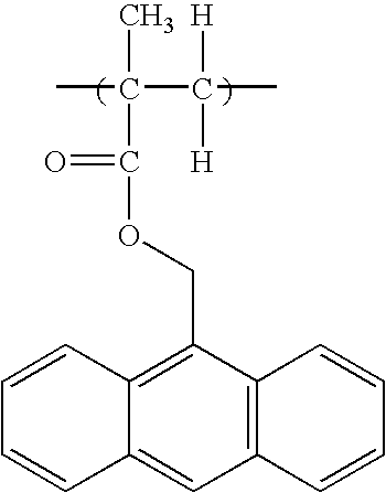
[Chemical Formula 9] Formula (a4)
(where R1 means the same as R1 defined in the formula (a1), and B2 is a substituted or unsubstituted benzene ring or an anthracene ring).


(where each R independently represents a hydrogen atom, a hydroxyl group, a cyclic or chain alkyl group having carbon atom(s) of 1 to 10, an alkoxy group having carbon atom(s) of 1 to 10, an aralkyl group having carbon atoms of 7 to 15, an aryl group having carbon atoms of 6 to 14, an aryloxyalkyl group having carbon atoms of 7 to 15, an alkenyl group having carbon atoms of 2 to 10 or an alkoxyalkyl group having carbon atoms of 2 to 10, and m is the number of repeating units and represents 10 to 300), a formula (b1-2):

(where R and m mean the same as defined in the formula (b1-1)), or a combination thereof.

(where R and m mean the same as defined in the formula (b1-1)), a formula (b2-2):

(where R and m mean the same as defined in the formula (b1-1)), the formula (b2-3):

(where m means the same as defined in the formula (b1-1)), or a combination thereof. In the formula (b2-1) to the formula (b2-3), each R can be selected from a type of the substituents shown in the formula (b1-1). In addition, m can be selected from the same range as shown in the formula (b1-1). Examples of the polysiloxane (b2) include a polymer having a structure of the formula (b2-1), a polymer having a structure of the formula (b2-2), a polymer having a structure of the formula (b2-3), a polymer having structures of the formula (b2-1) and the formula (b2-2), a polymer having structures of the formula (b2-1) and the formula (b2-3), a polymer having structures of the formula (b2-2) and the formula (b2-3), and a polymer having structures of the formula (b2-1), the formula (b2-2) and the formula (b2-3).

(where R and m mean the same as defined in the formula (b1-1)), the formula (b3-2):

(where R and m mean the same as defined in the formula (b1-1), and n is the number of repeating units and represents 1 to 10), or a combination thereof.


with a compound represented by a formula (c2-15).


| TABLE 1 | |||||
| Compound | |||||
| number | A1 | A2 | A3 | X | M |
| 1 | H | H | H | OC(═O) | Ph-2,4-(Br)2 |
| 2 | H | H | H | OC(═O) | Ph |
| 3 | H | H | H | OC(═O) | Ph-4-NO2 |
| 4 | H | CH3 | H | OC(═O) | Ph |
| 5 | H | H | H | OC(═O) | Ph-3-CN |
| 6 | H | H | H | OC(═O) | Ph-3-CH3 |
| 7 | H | H | H | OC(═O) | Ph-2-OCH3 |
| 8 | H | H | H | OC(═O) | Ph-2,3,5-(I)3 |
| 9 | H | CH3 | H | OC(═O) | Ph-3-Br-5-I |
| 10 | H | H | H | OC(═O) | Ph-2,3,4,5-(I)4 |
| 11 | H | H | H | OC(═O) | Ph-3-SCH3 |
| 12 | H | H | H | OC(═O) | Ph-2,4-(Cl)3 |
| 13 | H | H | H | OC(═O) | Ph-2-Br-4-CH3 |
| 14 | H | H | H | OC(═O) | Ph-3-Br-5-I |
| 15 | H | H | H | OC(═O) | 1-Nap-6-OCH3 |
| 16 | H | H | H | OC(═O) | 2-Nap-3-CH3 |
| 17 | H | CH3 | H | OC(═O) | 1-Nap |
| 18 | H | H | H | OC(═O) | 2-Nap-6-F |
| 19 | H | H | H | OC(═O) | 9-Ant |
| 20 | H | H | H | OC(═O) | 9-Ant-10-Br |
| 21 | H | H | H | S | Ph-4-F |
| 22 | H | H | H | S | Ph |
| 23 | H | H | H | S | Ph-3-CH3 |
| 24 | H | H | H | S | Ph-2,4-(Cl)3 |
| 25 | H | H | H | S | Ph-2,4-(Br)2 |
| 26 | H | H | H | S | 1-Nap |
| 27 | H | H | H | S | 2-Nap-6,7-(Br)2 |
| 28 | H | H | H | S | 9-Ant |
| 29 | H | H | H | NH | Ph |
| 30 | H | CH3 | H | NH | Ph |
| 31 | H | H | H | NH | Ph-4-CH3 |
| 32 | H | H | H | NH | Ph-2-Br |
| 33 | H | H | H | NH | Ph-3,5-(Br)2 |
| 34 | H | H | H | NH | Ph-3-CN |
| 35 | H | H | H | NH | Ph-3-COOCH3 |
| 36 | H | H | H | NH | Ph-3,4,5-(Cl)3 |
| 37 | H | H | H | NH | Ph-4-SCH3 |
| 38 | H | H | H | NH | Ph-2-F-4-Cl |
| 39 | H | H | H | NH | Ph-3-CH3 |
| 40 | H | H | H | NH | 1-Nap |
| 41 | H | H | H | O | Ph-2-Br |
| 42 | H | CH3 | H | O | Ph |
| 43 | H | H | H | O | Ph-2,4-Br2 |
| 44 | H | H | H | O | Ph-4-CH3 |
| 45 | H | H | H | O | Ph-3-I |
| 46 | H | H | H | O | Ph-2-F |
| 47 | H | H | H | O | Ph-3-OCH3 |
| 48 | H | H | H | O | Ph-3-NO2 |
| 49 | H | H | H | O | 1-Nap-2-Cl |
| 50 | H | CH3 | H | O | 1-Nap |
| 51 | H | H | H | O | 2-Nap |
| 52 | H | H | H | O | 9-Ant |


(where each of A1, A2 and A3 independently represents a hydrogen group, a methyl group or an ethyl group), is reacted with a phenyl compound or a naphthalene compound represented by a formula (c2-7):
[Chemical Formula 28]
HO—Y—Ar—Y—CH (c 2-7)
(where Y represents a direct bonding or —C(═O)—; Ar represents a benzene ring or a naphthalene ring which may be substituted with an alkyl group having carbon atom(s) of 1 to 6, a phenyl group, a naphthyl group, a halogen atom, an alkoxycarbonyl group having carbon atom(s) of 1 to 6, a nitro group, a carboxyl group, a cyano group, an alkoxy group having carbon atom(s) of 1 to 6, a hydroxy group, a thiol group, an alkylthio group having carbon atom(s) of 1 to 6 or an amino group). In this reaction, although the compound represented by the formula (c2-7) can be used singly, the compounds can also be used in combination of two or more types. This reaction is preferably performed in the solution state in which these compounds are dissolved in organic solvents such as benzene, toluene, xylene, ethyl lactate, butyl lactate, propylene glycol monomethyl ether, propylene glycol monomethyl ether acetate, and N-methylpyrrolidone. In addition, quaternary ammonium salts such as benzyltriethylammonium chloride, tetrabutylammonium chloride, tetraethylammonium bromide can be used as catalysts of this reaction. Although the reaction time and the reaction temperature of this reaction depend on compounds, a concentration and the like to be used, they are appropriately selected from the range of the reaction time of 0.1 to 100 hours and the reaction temperature of 20° C. to 200° C. When a catalyst is used, it can be used in a range of 0.001 to 50% by mass to the total mass of compounds used.


(where B represents a hydrogen atom, an alkyl group having carbon atom(s) of 1 to 6, a phenyl group, a naphthyl group, a halogen atom, an alkoxycarbonyl group having carbon atom(s) of 1 to 6, a nitro group, a carboxyl group, a cyano group, an alkoxy group having carbon atom(s) of 1 to 6, a hydroxy group, a thiol group, an alkylthio group having carbon atom(s) of 1 to 6 or an amino group; n represents the number of 1 to 6; m represents the number of 1 to 4, and when n and m are 2 or more, B may be the same or different). In the reaction, although the compounds of the formulae (c2-9) to (c2-14) can be used singly, the compounds can also be used in combination of two or more types.


5.0 g of KN 030 (manufactured by Osaka Organic Chemical Industry Ltd., a component is a copolymer of naphthol novolac and cresol novolac, and a ratio of copolymer is naphthol novolac of 70 mol % and cresol novolac of 30 mol %, and a weight average molecule weight is 1500), and 2.50 g of tetramethoxymethyl glycoluryl and 0.125 g of pyridinium-p-toluenesulfonic acid were added to 114.5 g of propylene glycol monomethyl ether acetate to be a 10.0% by mass solution. The solution was filtrated by using a microfilter made of polyethylene having a pore diameter of 0.2 μm to prepare the solution of the silicon-containing hard mask (layer B) forming composition.

| TABLE 2 |
| Ratios of dry etching rate |
| Layer C/ | Layer B/ | Layer A/ | SiO2 on substrate/ | ||
| Layer D | Layer C | Layer B | Layer A | ||
| Example 1 | 1.3 | 1.4 | 25 | 15 |
| Example 2 | 1.3 | 1.3 | 20 | 15 |
(Table 4)
| TABLE 3 |
| Ratios of dry etching rate |
| Layer B/ | Layer A/ | SiO2 on substrate/ | ||
| Layer D | Layer B | Layer A | ||
| Comparative | 1.4 | 25 | 15 | ||
| Example 1 | |||||
| Comparative | 1.4 | 25 | 15 | ||
| Example 2 | |||||
| TABLE 4 |
| Measurement of focus depth margin |
| Focus depth | Limiting | Bottom shape | ||
| margin (μm) | resolution (nm) | of resist | ||
| Example 1 | 0.7 | 80 | Good |
| Example 2 | 0.7 | 80 | Good |
| Comparative | — | 100 | Skirt shape |
| Example 1 | |||
| Comparative | — | 100 | Skirt shape |
| Example 2 | |||
Claims (10)
Applications Claiming Priority (3)
| Application Number | Priority Date | Filing Date | Title |
|---|---|---|---|
| JP2006279060 | 2006-10-12 | ||
| JP2006-279060 | 2006-10-12 | ||
| PCT/JP2007/069973 WO2008047715A1 (en) | 2006-10-12 | 2007-10-12 | Method for manufacturing semiconductor device using quadruple-layer laminate |
Publications (2)
| Publication Number | Publication Date |
|---|---|
| US20100022089A1 US20100022089A1 (en) | 2010-01-28 |
| US7842620B2 true US7842620B2 (en) | 2010-11-30 |
Family
ID=39313946
Family Applications (1)
| Application Number | Title | Priority Date | Filing Date |
|---|---|---|---|
| US12/311,742 Active US7842620B2 (en) | 2006-10-12 | 2007-10-12 | Method for manufacturing semiconductor device using quadruple-layer laminate |
Country Status (7)
| Country | Link |
|---|---|
| US (1) | US7842620B2 (en) |
| EP (1) | EP2085823B1 (en) |
| JP (1) | JP5057107B2 (en) |
| KR (1) | KR101423058B1 (en) |
| CN (1) | CN101523292B (en) |
| TW (1) | TWI427423B (en) |
| WO (1) | WO2008047715A1 (en) |
Cited By (3)
| Publication number | Priority date | Publication date | Assignee | Title |
|---|---|---|---|---|
| US20100266951A1 (en) * | 2007-12-13 | 2010-10-21 | Nissan Chemical Industries, Ltd. | Resist underlayer film forming composition and method for forming resist pattern |
| US20130284699A1 (en) * | 2012-04-27 | 2013-10-31 | Shin-Etsu Chemical Co., Ltd. | Patterning process |
| US20140220783A1 (en) * | 2011-10-12 | 2014-08-07 | Jsr Corporation | Pattern-forming method and resist underlayer film-forming composition |
Families Citing this family (28)
| Publication number | Priority date | Publication date | Assignee | Title |
|---|---|---|---|---|
| JP5343580B2 (en) * | 2008-10-02 | 2013-11-13 | Jsr株式会社 | Composition for forming silicon-containing film for multilayer resist process |
| CN102227813B (en) * | 2008-11-28 | 2013-12-25 | 日产化学工业株式会社 | Forming agent for gate dielectric film of thin film transistor |
| JP5038354B2 (en) * | 2009-05-11 | 2012-10-03 | 信越化学工業株式会社 | Silicon-containing antireflection film-forming composition, silicon-containing antireflection film-forming substrate, and pattern formation method |
| US8431670B2 (en) * | 2009-08-31 | 2013-04-30 | International Business Machines Corporation | Photo-patternable dielectric materials and formulations and methods of use |
| JP5696428B2 (en) * | 2009-10-30 | 2015-04-08 | Jsr株式会社 | Reverse pattern forming method and polysiloxane resin composition |
| US8395228B2 (en) | 2010-11-08 | 2013-03-12 | International Business Machines Corporation | Integration process to improve focus leveling within a lot process variation |
| JPWO2012081619A1 (en) * | 2010-12-17 | 2014-05-22 | 日産化学工業株式会社 | Resist underlayer film forming composition and resist pattern forming method using the same |
| KR101876600B1 (en) * | 2011-03-30 | 2018-07-09 | 제이에스알 가부시끼가이샤 | Multilayer resist process pattern forming method and inorganic film forming composition for multilayer resist process |
| EP2735904A4 (en) * | 2011-07-20 | 2014-11-26 | Nissan Chemical Ind Ltd | Thin film formation composition for lithography which contains titanium and silicon |
| JP5970933B2 (en) * | 2011-09-15 | 2016-08-17 | Jsr株式会社 | Pattern formation method |
| US9011591B2 (en) * | 2011-09-21 | 2015-04-21 | Dow Global Technologies Llc | Compositions and antireflective coatings for photolithography |
| TWI582180B (en) * | 2011-12-21 | 2017-05-11 | 陶氏全球科技有限責任公司 | Compositions for antireflective coatings |
| JP6237616B2 (en) * | 2012-02-27 | 2017-11-29 | 三菱瓦斯化学株式会社 | Acid-treated monoalkylnaphthalene formaldehyde resin |
| JP2014091743A (en) * | 2012-10-31 | 2014-05-19 | Olympus Corp | Coating material, optical coating film and optical element |
| KR20140081022A (en) * | 2012-12-21 | 2014-07-01 | 삼성전기주식회사 | Dry film photoresist having oxygen permeable barrier layer and manufacturing method thereof |
| WO2015098525A1 (en) * | 2013-12-27 | 2015-07-02 | 日産化学工業株式会社 | Resist underlayer film-forming composition containing copolymer that has triazine ring and sulfur atom in main chain |
| KR102358183B1 (en) * | 2014-05-22 | 2022-02-04 | 닛산 가가쿠 가부시키가이샤 | Resist underlayer film forming composition for lithography containing polymer that contains blocked isocyanate structure |
| JP6196190B2 (en) * | 2014-07-08 | 2017-09-13 | 信越化学工業株式会社 | Multilayer film forming method and pattern forming method |
| JP6243815B2 (en) * | 2014-09-01 | 2017-12-06 | 信越化学工業株式会社 | Manufacturing method of semiconductor device substrate |
| US20180181001A1 (en) * | 2015-07-02 | 2018-06-28 | Nissan Chemical Industries, Ltd. | Resist underlayer film-forming composition comprising epoxy adduct having long-chain alkyl group |
| US20200201183A1 (en) * | 2016-07-15 | 2020-06-25 | Nissan Chemical Corporation | Resist underlayer film forming composition containing compound having hydantoin ring |
| CN109923368A (en) | 2016-12-13 | 2019-06-21 | 金泰克斯公司 | Biometrical identification systems for rifle |
| KR102067081B1 (en) | 2017-11-01 | 2020-01-16 | 삼성에스디아이 주식회사 | Resist underlayer composition, and method of forming patterns using the composition |
| US11437237B2 (en) * | 2018-02-28 | 2022-09-06 | Central Glass Company, Limited | Silicon-containing layer-forming composition, and method for producing pattern-equipped substrate which uses same |
| US20210166938A1 (en) * | 2018-04-11 | 2021-06-03 | Wisys Technology Foundation, Inc. | Macromolecular sieves from semiconductor membranes for shape-based separation and sensing |
| KR102428640B1 (en) * | 2021-02-22 | 2022-08-02 | 인하대학교 산학협력단 | Method for Dry Etching of Copper Thin Films |
| KR20240004468A (en) * | 2021-04-30 | 2024-01-11 | 닛산 가가쿠 가부시키가이샤 | Composition for forming a silicon-containing resist underlayer film |
| WO2023204287A1 (en) * | 2022-04-22 | 2023-10-26 | 日産化学株式会社 | Composition for resist underlayer film formation |
Citations (33)
| Publication number | Priority date | Publication date | Assignee | Title |
|---|---|---|---|---|
| US5767018A (en) * | 1995-11-08 | 1998-06-16 | Advanced Micro Devices, Inc. | Method of etching a polysilicon pattern |
| JPH11258813A (en) | 1998-03-13 | 1999-09-24 | Jsr Corp | Composition for forming antireflection film and antireflection film |
| US5986344A (en) * | 1998-04-14 | 1999-11-16 | Advanced Micro Devices, Inc. | Anti-reflective coating layer for semiconductor device |
| US6103456A (en) * | 1998-07-22 | 2000-08-15 | Siemens Aktiengesellschaft | Prevention of photoresist poisoning from dielectric antireflective coating in semiconductor fabrication |
| JP2000232107A (en) | 1999-02-12 | 2000-08-22 | Mitsubishi Electric Corp | Pattern forming method of semiconductor device |
| JP2001053068A (en) | 1999-06-11 | 2001-02-23 | Shipley Co Llc | Reflection preventing hard mask composition |
| US6207573B1 (en) * | 1999-05-19 | 2001-03-27 | Infineon Technologies North America Corp. | Differential trench open process |
| US6309955B1 (en) * | 2001-02-16 | 2001-10-30 | Advanced Micro Devices, Inc. | Method for using a CVD organic barc as a hard mask during via etch |
| WO2002005035A1 (en) | 2000-07-12 | 2002-01-17 | Nissan Chemical Industries, Ltd. | Lithographic gap-filler forming composition |
| JP2002047430A (en) | 2000-04-24 | 2002-02-12 | Shipley Co Llc | Composition for filling aperture |
| JP2002128847A (en) | 2000-07-14 | 2002-05-09 | Shipley Co Llc | Barrier composition |
| US6444584B1 (en) * | 1998-07-16 | 2002-09-03 | Taiwan Semiconductor Manufacturing Company | Plasma etch method for forming composite silicon/dielectric/silicon stack layer |
| WO2003017002A1 (en) | 2001-08-20 | 2003-02-27 | Nissan Chemical Industries, Ltd. | Composition for forming antireflective film for use in lithography |
| JP2003297920A (en) | 2002-04-03 | 2003-10-17 | Nec Corp | Manufacturing method of semiconductor device |
| US6638871B2 (en) * | 2002-01-10 | 2003-10-28 | United Microlectronics Corp. | Method for forming openings in low dielectric constant material layer |
| WO2004034148A1 (en) | 2002-10-09 | 2004-04-22 | Nissan Chemical Industries, Ltd. | Composition for forming antireflection film for lithography |
| JP2004152997A (en) | 2002-10-30 | 2004-05-27 | Fujitsu Ltd | Method of manufacturing semiconductor device |
| US6797610B1 (en) * | 2002-12-11 | 2004-09-28 | International Business Machines Corporation | Sublithographic patterning using microtrenching |
| US20040247900A1 (en) | 2003-06-03 | 2004-12-09 | Tsutomu Ogihara | Antireflective film material, and antireflective film and pattern formation method using the same |
| JP2005015779A (en) | 2003-06-03 | 2005-01-20 | Shin Etsu Chem Co Ltd | Material for antireflection film, antireflection film using the material, and pattern forming method |
| JP2005018054A (en) | 2003-06-03 | 2005-01-20 | Shin Etsu Chem Co Ltd | Antireflection film material, antireflection film using the same and pattern forming method |
| JP2005055893A (en) | 2003-08-05 | 2005-03-03 | Internatl Business Mach Corp <Ibm> | Lithographic antireflective hardmask composition and method for manufacturing semiconductor device by using the same |
| US6878646B1 (en) * | 2002-10-16 | 2005-04-12 | Taiwan Semiconductor Manufacturing Company | Method to control critical dimension of a hard masked pattern |
| WO2005098542A1 (en) | 2004-04-09 | 2005-10-20 | Nissan Chemical Industries, Ltd. | Antireflection film for semiconductor containing condensation type polymer |
| US20060024945A1 (en) | 2004-07-29 | 2006-02-02 | Hynix Semiconductor, Inc. | Method for fabricating semiconductor device using amorphous carbon layer as sacrificial hard mask |
| US7005386B1 (en) * | 2003-09-05 | 2006-02-28 | Advanced Micro Devices, Inc. | Method for reducing resist height erosion in a gate etch process |
| US7015133B2 (en) * | 2004-04-14 | 2006-03-21 | Taiwan Semiconductor Manufacturing Company | Dual damascene structure formed of low-k dielectric materials |
| US7078350B2 (en) * | 2004-03-19 | 2006-07-18 | Lam Research Corporation | Methods for the optimization of substrate etching in a plasma processing system |
| WO2006115074A1 (en) | 2005-04-19 | 2006-11-02 | Nissan Chemical Industries, Ltd. | Composition comprising polymer having ethylene-dicarbonyl structure for use in forming anti-reflective coating for lithography |
| US7176571B2 (en) * | 2004-01-08 | 2007-02-13 | Taiwan Semiconductor Manufacturing Company | Nitride barrier layer to prevent metal (Cu) leakage issue in a dual damascene structure |
| US7211519B2 (en) * | 2003-04-30 | 2007-05-01 | Fujitsu Limited | Method for manufacturing semiconductor device |
| US20070142617A1 (en) | 2005-12-15 | 2007-06-21 | Hynix Semiconductor Inc. | Polymer for hard mask of semiconductor device and composition containing the same |
| US20070154839A1 (en) | 2006-01-02 | 2007-07-05 | Hynix Semiconductor Inc. | Hard mask composition for lithography process |
Family Cites Families (5)
| Publication number | Priority date | Publication date | Assignee | Title |
|---|---|---|---|---|
| JP3923755B2 (en) * | 2001-07-12 | 2007-06-06 | 株式会社東芝 | refrigerator |
| TWI276153B (en) * | 2001-11-12 | 2007-03-11 | Hynix Semiconductor Inc | Method for fabricating semiconductor device |
| CN100547487C (en) * | 2002-10-09 | 2009-10-07 | 日产化学工业株式会社 | The photoetching composition that forms antireflection film |
| KR100500453B1 (en) * | 2003-06-23 | 2005-07-12 | 삼성전자주식회사 | method of formation under layer in a bi-layer resist film |
| JP2006024811A (en) * | 2004-07-09 | 2006-01-26 | Sony Corp | Method for manufacturing semiconductor device |
-
2007
- 2007-10-12 US US12/311,742 patent/US7842620B2/en active Active
- 2007-10-12 JP JP2008539789A patent/JP5057107B2/en active Active
- 2007-10-12 EP EP07829709A patent/EP2085823B1/en active Active
- 2007-10-12 TW TW096138270A patent/TWI427423B/en active
- 2007-10-12 WO PCT/JP2007/069973 patent/WO2008047715A1/en active Application Filing
- 2007-10-12 CN CN200780037889.9A patent/CN101523292B/en active Active
- 2007-10-12 KR KR1020097008261A patent/KR101423058B1/en active IP Right Grant
Patent Citations (41)
| Publication number | Priority date | Publication date | Assignee | Title |
|---|---|---|---|---|
| US5767018A (en) * | 1995-11-08 | 1998-06-16 | Advanced Micro Devices, Inc. | Method of etching a polysilicon pattern |
| JPH11258813A (en) | 1998-03-13 | 1999-09-24 | Jsr Corp | Composition for forming antireflection film and antireflection film |
| US5986344A (en) * | 1998-04-14 | 1999-11-16 | Advanced Micro Devices, Inc. | Anti-reflective coating layer for semiconductor device |
| US6444584B1 (en) * | 1998-07-16 | 2002-09-03 | Taiwan Semiconductor Manufacturing Company | Plasma etch method for forming composite silicon/dielectric/silicon stack layer |
| US6103456A (en) * | 1998-07-22 | 2000-08-15 | Siemens Aktiengesellschaft | Prevention of photoresist poisoning from dielectric antireflective coating in semiconductor fabrication |
| US6287752B1 (en) | 1999-02-12 | 2001-09-11 | Mitsubishi Denki Kabushiki Kaisha | Semiconductor device, method of manufacturing a semiconductor device, and method of forming a pattern for semiconductor device |
| JP2000232107A (en) | 1999-02-12 | 2000-08-22 | Mitsubishi Electric Corp | Pattern forming method of semiconductor device |
| US6207573B1 (en) * | 1999-05-19 | 2001-03-27 | Infineon Technologies North America Corp. | Differential trench open process |
| JP2001053068A (en) | 1999-06-11 | 2001-02-23 | Shipley Co Llc | Reflection preventing hard mask composition |
| US6890448B2 (en) * | 1999-06-11 | 2005-05-10 | Shipley Company, L.L.C. | Antireflective hard mask compositions |
| JP2002047430A (en) | 2000-04-24 | 2002-02-12 | Shipley Co Llc | Composition for filling aperture |
| WO2002005035A1 (en) | 2000-07-12 | 2002-01-17 | Nissan Chemical Industries, Ltd. | Lithographic gap-filler forming composition |
| JP2002128847A (en) | 2000-07-14 | 2002-05-09 | Shipley Co Llc | Barrier composition |
| US6309955B1 (en) * | 2001-02-16 | 2001-10-30 | Advanced Micro Devices, Inc. | Method for using a CVD organic barc as a hard mask during via etch |
| US20040197709A1 (en) | 2001-08-20 | 2004-10-07 | Shinya Arase | Composition for forming anti-reflective coating for use in lithography |
| WO2003017002A1 (en) | 2001-08-20 | 2003-02-27 | Nissan Chemical Industries, Ltd. | Composition for forming antireflective film for use in lithography |
| US6638871B2 (en) * | 2002-01-10 | 2003-10-28 | United Microlectronics Corp. | Method for forming openings in low dielectric constant material layer |
| JP2003297920A (en) | 2002-04-03 | 2003-10-17 | Nec Corp | Manufacturing method of semiconductor device |
| WO2004034148A1 (en) | 2002-10-09 | 2004-04-22 | Nissan Chemical Industries, Ltd. | Composition for forming antireflection film for lithography |
| US20060290429A1 (en) | 2002-10-09 | 2006-12-28 | Nissan Chemical Industries, Ltd. | Composition form forming anti-reflective coating for use in lithography |
| US6878646B1 (en) * | 2002-10-16 | 2005-04-12 | Taiwan Semiconductor Manufacturing Company | Method to control critical dimension of a hard masked pattern |
| JP2004152997A (en) | 2002-10-30 | 2004-05-27 | Fujitsu Ltd | Method of manufacturing semiconductor device |
| US20040137711A1 (en) | 2002-10-30 | 2004-07-15 | Takatoshi Deguchi | Method for manufacturing semiconductor device |
| US6797610B1 (en) * | 2002-12-11 | 2004-09-28 | International Business Machines Corporation | Sublithographic patterning using microtrenching |
| US7211519B2 (en) * | 2003-04-30 | 2007-05-01 | Fujitsu Limited | Method for manufacturing semiconductor device |
| JP2005018054A (en) | 2003-06-03 | 2005-01-20 | Shin Etsu Chem Co Ltd | Antireflection film material, antireflection film using the same and pattern forming method |
| JP2005015779A (en) | 2003-06-03 | 2005-01-20 | Shin Etsu Chem Co Ltd | Material for antireflection film, antireflection film using the material, and pattern forming method |
| US20040247900A1 (en) | 2003-06-03 | 2004-12-09 | Tsutomu Ogihara | Antireflective film material, and antireflective film and pattern formation method using the same |
| JP2005055893A (en) | 2003-08-05 | 2005-03-03 | Internatl Business Mach Corp <Ibm> | Lithographic antireflective hardmask composition and method for manufacturing semiconductor device by using the same |
| US7005386B1 (en) * | 2003-09-05 | 2006-02-28 | Advanced Micro Devices, Inc. | Method for reducing resist height erosion in a gate etch process |
| US7176571B2 (en) * | 2004-01-08 | 2007-02-13 | Taiwan Semiconductor Manufacturing Company | Nitride barrier layer to prevent metal (Cu) leakage issue in a dual damascene structure |
| US7078350B2 (en) * | 2004-03-19 | 2006-07-18 | Lam Research Corporation | Methods for the optimization of substrate etching in a plasma processing system |
| WO2005098542A1 (en) | 2004-04-09 | 2005-10-20 | Nissan Chemical Industries, Ltd. | Antireflection film for semiconductor containing condensation type polymer |
| US7015133B2 (en) * | 2004-04-14 | 2006-03-21 | Taiwan Semiconductor Manufacturing Company | Dual damascene structure formed of low-k dielectric materials |
| JP2006041486A (en) | 2004-07-29 | 2006-02-09 | Hynix Semiconductor Inc | Manufacturing method of semiconductor device using amorphous carbon film as sacrifice hard mask |
| US20060024945A1 (en) | 2004-07-29 | 2006-02-02 | Hynix Semiconductor, Inc. | Method for fabricating semiconductor device using amorphous carbon layer as sacrificial hard mask |
| WO2006115074A1 (en) | 2005-04-19 | 2006-11-02 | Nissan Chemical Industries, Ltd. | Composition comprising polymer having ethylene-dicarbonyl structure for use in forming anti-reflective coating for lithography |
| US20070142617A1 (en) | 2005-12-15 | 2007-06-21 | Hynix Semiconductor Inc. | Polymer for hard mask of semiconductor device and composition containing the same |
| JP2007161985A (en) | 2005-12-15 | 2007-06-28 | Hynix Semiconductor Inc | Polymer for hard mask for semiconductor element and composition containing the polymer |
| US20070154839A1 (en) | 2006-01-02 | 2007-07-05 | Hynix Semiconductor Inc. | Hard mask composition for lithography process |
| JP2007193308A (en) | 2006-01-02 | 2007-08-02 | Hynix Semiconductor Inc | Hard mask composition for lithography process |
Non-Patent Citations (4)
| Title |
|---|
| Crawford et al., "New Materials for 157 nm Photoresists: Characterization and Properties," Proceedings of SPIE, 2000, pp. 357-364, vol. 3999. |
| Patterson et al., "Polymers for 157 nm Photoresist Applications: A Progress Report," Proceedings of SPIE, 2000, pp. 365-374, vol. 3999. |
| Schmaljohann et al., "Design Strategies for 157 nm Single-Layer Photoresists: Lithographic Evaluation of a Poly (alpha-trifluoromethyl vinyl alcohol) Copolymer," Proceedings of SPIE, 2000, pp. 330-334, vol. 3999. |
| Schmaljohann et al., "Design Strategies for 157 nm Single-Layer Photoresists: Lithographic Evaluation of a Poly (α-trifluoromethyl vinyl alcohol) Copolymer," Proceedings of SPIE, 2000, pp. 330-334, vol. 3999. |
Cited By (6)
| Publication number | Priority date | Publication date | Assignee | Title |
|---|---|---|---|---|
| US20100266951A1 (en) * | 2007-12-13 | 2010-10-21 | Nissan Chemical Industries, Ltd. | Resist underlayer film forming composition and method for forming resist pattern |
| US8361695B2 (en) * | 2007-12-13 | 2013-01-29 | Nissan Chemical Industries, Ltd. | Resist underlayer film forming composition and method for forming resist pattern |
| US20140220783A1 (en) * | 2011-10-12 | 2014-08-07 | Jsr Corporation | Pattern-forming method and resist underlayer film-forming composition |
| US9607849B2 (en) * | 2011-10-12 | 2017-03-28 | Jsr Corporation | Pattern-forming method and resist underlayer film-forming composition |
| US20130284699A1 (en) * | 2012-04-27 | 2013-10-31 | Shin-Etsu Chemical Co., Ltd. | Patterning process |
| US8992790B2 (en) * | 2012-04-27 | 2015-03-31 | Shin-Etsu Chemical Co., Ltd. | Patterning process |
Also Published As
| Publication number | Publication date |
|---|---|
| EP2085823A4 (en) | 2011-05-25 |
| JP5057107B2 (en) | 2012-10-24 |
| WO2008047715A1 (en) | 2008-04-24 |
| TW200834245A (en) | 2008-08-16 |
| CN101523292B (en) | 2013-04-10 |
| EP2085823A1 (en) | 2009-08-05 |
| CN101523292A (en) | 2009-09-02 |
| KR101423058B1 (en) | 2014-07-25 |
| TWI427423B (en) | 2014-02-21 |
| KR20090082191A (en) | 2009-07-29 |
| JPWO2008047715A1 (en) | 2010-02-25 |
| US20100022089A1 (en) | 2010-01-28 |
| EP2085823B1 (en) | 2013-01-16 |
Similar Documents
| Publication | Publication Date | Title |
|---|---|---|
| US7842620B2 (en) | Method for manufacturing semiconductor device using quadruple-layer laminate | |
| TWI450041B (en) | Resist underlayer coating forming composition comprising polymer containing nitrogen-containing silyl group | |
| TWI467338B (en) | Resist underlayer film forming composition containing silicone having cyclic amino group | |
| JP6066092B2 (en) | Diarylamine novolac resin | |
| TWI648598B (en) | Resist underlayer coating composition containing silicone having anionic group | |
| TWI477916B (en) | Resist underlayer forming composition containing silicon having onium group | |
| JP6094767B2 (en) | Resist underlayer film forming composition containing phenylindole-containing novolak resin | |
| US10437150B2 (en) | Composition for forming resist underlayer film with reduced outgassing | |
| TWI450042B (en) | Resist underlayer coating forming composition containing silicon having blocked isocyanate group | |
| JP5067537B2 (en) | Resist underlayer film forming composition containing polynuclear phenol | |
| TWI507825B (en) | Silicon-containing resist underlayer film forming composition containing amic acid | |
| WO2013115097A1 (en) | Resist underlayer film forming composition containing copolymer resin having heterocyclic ring | |
| TW201432386A (en) | Resist underlayer film forming composition containing silicon having ester group | |
| US20220373888A1 (en) | Silicon-containing resist underlayer film-forming composition including organic group having ammonium group | |
| JP7388022B2 (en) | Resist underlayer film forming composition using polymeric crosslinking agent | |
| US20160186006A1 (en) | Resist underlayer film-forming composition containing polymer which contains nitrogen-containing ring compound | |
| JP7306451B2 (en) | Resist underlayer film-forming composition containing alicyclic compound-terminated polymer | |
| CN113891906A (en) | Film-forming composition | |
| JP4831330B2 (en) | Resist underlayer film forming composition containing polycarbosilane | |
| US11131928B2 (en) | Resist underlayer film forming composition which contains compound having glycoluril skeleton as additive | |
| JP6338048B2 (en) | Iminostilbene polymer and resist underlayer film forming composition containing the same | |
| CN116635442A (en) | Composition for forming resist underlayer film | |
| KR20220079900A (en) | Resist underlayer film forming composition | |
| KR20200123117A (en) | A composition for forming a resist underlayer film comprising a novolac resin containing triaryldiamine added with an aromatic vinyl compound | |
| US20220206395A1 (en) | Composition for resist pattern metallization process |
Legal Events
| Date | Code | Title | Description |
|---|---|---|---|
| AS | Assignment |
Owner name: NISSAN CHEMICAL INDUSTRIES, LTD., JAPAN Free format text: ASSIGNMENT OF ASSIGNORS INTEREST;ASSIGNORS:TAKEI, SATOSHI;NAKAJIMA, MAKOTO;SAKAIDA, YASUSHI;AND OTHERS;REEL/FRAME:022777/0546 Effective date: 20090526 |
|
| STCF | Information on status: patent grant |
Free format text: PATENTED CASE |
|
| FEPP | Fee payment procedure |
Free format text: PAYOR NUMBER ASSIGNED (ORIGINAL EVENT CODE: ASPN); ENTITY STATUS OF PATENT OWNER: LARGE ENTITY |
|
| FPAY | Fee payment |
Year of fee payment: 4 |
|
| MAFP | Maintenance fee payment |
Free format text: PAYMENT OF MAINTENANCE FEE, 8TH YEAR, LARGE ENTITY (ORIGINAL EVENT CODE: M1552) Year of fee payment: 8 |
|
| MAFP | Maintenance fee payment |
Free format text: PAYMENT OF MAINTENANCE FEE, 12TH YEAR, LARGE ENTITY (ORIGINAL EVENT CODE: M1553); ENTITY STATUS OF PATENT OWNER: LARGE ENTITY Year of fee payment: 12 |