US7830893B2 - Real time segmentation and reassembly of asynchronous transfer mode (ATM) adaptation layer two (AAL2) and AAL5 data - Google Patents
Real time segmentation and reassembly of asynchronous transfer mode (ATM) adaptation layer two (AAL2) and AAL5 data Download PDFInfo
- Publication number
- US7830893B2 US7830893B2 US10/791,117 US79111704A US7830893B2 US 7830893 B2 US7830893 B2 US 7830893B2 US 79111704 A US79111704 A US 79111704A US 7830893 B2 US7830893 B2 US 7830893B2
- Authority
- US
- United States
- Prior art keywords
- atm
- cell
- cells
- vci
- aal
- Prior art date
- Legal status (The legal status is an assumption and is not a legal conclusion. Google has not performed a legal analysis and makes no representation as to the accuracy of the status listed.)
- Active, expires
Links
Images


Classifications
-
- H—ELECTRICITY
- H04—ELECTRIC COMMUNICATION TECHNIQUE
- H04L—TRANSMISSION OF DIGITAL INFORMATION, e.g. TELEGRAPHIC COMMUNICATION
- H04L12/00—Data switching networks
- H04L12/54—Store-and-forward switching systems
- H04L12/56—Packet switching systems
- H04L12/5601—Transfer mode dependent, e.g. ATM
Definitions
- ATM Asynchronous transfer mode
- ATM is a communication protocol that has continually gained in popularity and continues to be used as the preferred communication protocol for high-speed fiber optic-based communication networks.
- ATM is a packet-based communication protocol that communicates by transmitting and receiving packets, referred to as “cells.”
- Each ATM cell comprises a header portion and a payload portion.
- the header portion comprises five bytes (also referred to as “octets”) of information and the payload portion comprises 48 octets.
- the header portion contains information that defines the type of ATM cell and the payload. In some instances, the payload portion of multiple cells is combined (typically by concatenation) to form a larger packet.
- ATM adaptation layer 5 AAL5
- VCC virtual channel connection
- CPE customer premises equipment
- a segmentation and reassembly (SAR) function is performed to segment the communication data into ATM cells at the source end and to reassemble the ATM cells into communication data at the destination end.
- segmentation and reassembly of ATM data requires significant processing resources and is difficult to perform in real-time. This situation is particularly troublesome when attempting to test, troubleshoot and gather statistics in an ATM network.
- Embodiments of the invention include a system for reassembling asynchronous transfer mode (ATM) data in real time, comprising a circular buffer for storing ATM data, the ATM data comprising information divided into cells, and a plurality of parallel processing elements configured to analyze the ATM cells and determine a cell type, wherein ATM adaptation layer (AAL) 2 cells and AAL 5 cells are reassembled in real-time.
- ATM asynchronous transfer mode
- FIG. 1 is a block diagram illustrating an exemplary asynchronous transfer mode (ATM) network in which an analysis device including the system for reassembling ATM data in real time resides.
- ATM asynchronous transfer mode
- FIG. 2A is a block diagram illustrating an exemplary ATM cell.
- FIG. 2B is a block diagram illustrating an exemplary ATM mini-cell.
- FIG. 3 is a block diagram illustrating the segmentation and reassembly (SAR) logic executed by the analysis device of FIG. 1 .
- SAR segmentation and reassembly
- FIG. 4 is a block diagram illustrating the operation of the segmentation and reassembly logic contained in the FPGA of FIG. 3 .
- FIG. 5 is a block diagram illustrating the operation of the buffer manager of FIG. 4 .
- FIGS. 6A and 6B are a flow chart collectively illustrating the operation of one embodiment of the segmentation and reassembly logic.
- the system for reassembling asynchronous transfer mode (ATM) data in real time in accordance with embodiments of the invention can be implemented in software (e.g., firmware), hardware, or a combination thereof.
- the system for reassembling ATM data in real time is implemented primarily using a combination of hardware and software, in which executable code is executed in a field programmable gate array (FPGA).
- FPGA field programmable gate array
- the software portion of the system for reassembling ATM data in real time can be executed by a special or general-purpose computer, such as a personal computer (PC; IBM-compatible, Apple-compatible, or otherwise), workstation, minicomputer, or mainframe computer.
- the system for reassembling asynchronous transfer mode (ATM) data in real time may be implemented in other processing or computing devices, such as, for example but not limited to, a dedicated processor.
- FIG. 1 is a block diagram illustrating an exemplary asynchronous transfer mode (ATM) network 100 in which an analysis device 150 including the system for reassembling ATM data in real time resides.
- the network 100 comprises an ATM switch 114 coupled to an ATM switch 118 via connection 116 .
- the ATM switches 114 and 118 operate to route ATM traffic over connection 116 per the ATM communication standard.
- the connection 116 is referred to a network node interface (NNI).
- NNI network node interface
- the NNI 116 couples two or more ATM switches to form an ATM communication network.
- Customer premises equipment (CPE) 102 is coupled to the ATM switch 114 via connection 104 .
- Connection 104 is referred to a user network interface (UNI), and can comprise many different communication channels.
- UNI user network interface
- a UNI can be any communication channel over which a customer location communicates with an ATM switch, and can be, for example, a digital subscriber line (DSL), a coaxial connection for a cable modem, a T1 communication channel, an optical, or a wireless connection, etc.
- Customer premises location 110 includes customer premises equipment 106 and 108 coupled to the ATM switch 114 via connection 112 .
- Connection 112 is also a user network interface (UNI). Further, in this example, the customer premises equipment 106 and 108 is coupled via a local area network (LAN) 115 .
- LAN local area network
- an analysis device 150 including the system for reassembling ATM data in real time also referred to as “segmentation and reassembly logic” (to be described below), is coupled to any of the UNI connections or to the NNI connection 116 via connection 132 , which can be an optical fiber.
- connection 132 can be an optical fiber.
- the various user network interface connections and network node interface connections can be carried via different physical media, such as those complying with plesiochronous digital hierarchy (PDH) or synchronous digital hierarchy (SDH) standards.
- PDH plesiochronous digital hierarchy
- SDH synchronous digital hierarchy
- An ATM network also makes use of what are referred to as “virtual circuits” to transport information.
- a virtual circuit (VC) is defined using what is referred to as a “virtual channel connection” (VCC).
- VCC virtual channel connection
- a VCC is established between any source and any destination in an ATM network, regardless of the way that data is being routed across the network.
- customer premises equipment 124 , 128 , 102 , 106 , and 108 are considered “endpoints,” any of which can be a source or a destination of data in the form of ATM traffic.
- ATM is a connection oriented technology.
- a connection is established by signaling, i.e., by transmitting a setup request which traverses the network from the source to the destination endpoint.
- VCC virtual channel identifiers
- VCI virtual path identifiers
- VCI virtual path identifiers
- IMA inverse multiplexing over ATM
- a virtual path groups multiple VCs carried between two ATM entities and may also involve many ATM VP links.
- the VC's associated with a VP are globally switched without unbundling or processing the individual VC or changing its VCI.
- the cell sequence of each VC is preserved and the quality of service of the VP depends on that of its most demanding VC.
- the cell address mechanism uses both the VCI and the VPI, different VP's may also use the same VCI without conflict.
- FIG. 2A is a block diagram illustrating an exemplary ATM cell 200 .
- the ATM cell 200 comprises a five byte header portion 202 and a 48 byte payload portion 204 .
- the 48 byte payload portion 204 is also referred to as the information field.
- the first byte in the header 202 comprises the virtual path identifier (VPI) in the case of an NNI connection, or generic flow control (GFC) plus VPI in the case of a UNI connection.
- a first portion of four bits of the second byte also comprises the virtual path identifier, while the second portion of four bits of the second byte comprises the virtual channel identifier (VCI).
- the third byte in the header 202 also comprises the virtual channel identifier, as does a first portion of four bits of the fourth byte.
- a second portion of three bits of the fourth byte in the header 202 comprises a payload type (PT) indicator (PTI), while a third portion of one bit of the fourth byte comprises a cell loss priority (CLP) bit.
- the fifth byte of the header 202 comprises the header error correction (HEC) byte.
- a byte is also referred to as “octet.”
- FIG. 2B is a block diagram illustrating an exemplary ATM mini-cell 290 .
- a mini-cell is a structure that is particular to AAL2.
- the mini-cell 290 resides within an ATM cell payload portion 204 and can span two or more ATM cells.
- the ATM mini-cell 220 includes a header portion 222 and a payload portion 224 .
- the first byte in the header portion 222 contains the channel identifier (CID).
- the first portion of the second byte contains the length indicator (LI).
- the second portion of the second byte plus the first portion of the third byte contain part of the user-user indicator (UUI).
- the second portion of the third byte contains a header error correction field (HEC), which is different from the ATM cell HEC.
- CID channel identifier
- LI length indicator
- UUI user-user indicator
- HEC header error correction field
- ATM is a layer-based architecture. In terms of the ATM protocol stack, the ATM layer resides above the physical layer. The ATM layer provides cell transfer for all services and includes the ATM adaptation layer (AAL). The ATM adaptation layer provides service dependant functions to the layers above the AAL layer.
- ATM is a packet switching technology that directs traffic using identifiers (VPI/VCI) contained in the header 202 . However, unlike other packet technologies, ATM uses short, fixed length packets called cells. As described above, typically each cell is 53 bytes long. Inserting payload data into the 48 byte payload portion 204 is accomplished by the AAL.
- the AAL provides ATM the flexibility to carry different types of services within the same format. It should be understood that AAL is not a network process, but instead is performed by the network terminating equipment.
- ATM adaptation layer type two provides variable bit rate (VBR) timing sensitive services.
- VBR variable bit rate
- AAL2 is used to transport traffic where a strong timing relationship between the source and the destination is required, but in which the bit rate may vary. Examples include variable bit rate voice and compressed, for example using motion picture experts group (MPEG) coded video.
- MPEG motion picture experts group
- ATM adaptation layer type 5 also refer to as a “simple and efficient adaptation layer (SEAL),” is design to meet the requirements of local, high speed LAN implementations.
- SEAL simple and efficient adaptation layer
- AAL5 is used for connectionless or connection oriented VBR services.
- AAL5 is a format whereby one to n cells having like VPI/VCI have their payloads concatenated to form a larger packet.
- AAL2 is a format whereby within the AAL2 format, there are multiple mini-cells. Multiple mini cells having like VPI/VCI and channel identifier (CID) have their payload concatenated to form a larger packet.
- CID channel identifier
- the segmentation and reassembly logic 300 to be described below in FIG. 3 distinguishes between AAL2 cells and AAL5 cells, and reassemblies these cells in real time at network speeds approaching and exceeding optical carrier (OC) 12 speed (i.e., a line rate of 622.080 megabits per second (Mbps)).
- OC optical carrier
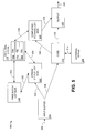
- FIG. 3 is a block diagram illustrating the segmentation and reassembly (SAR) logic 300 executed by the analysis device 150 of FIG. 1 .
- the segmentation and reassembly logic 300 comprises, in this embodiment, a line interface module (LIM) 306 including at least one LIM analog module 302 and a LIM digital module 304 .
- LIM line interface module
- a “module” can be a printed circuit card, or wiring board.
- the segmentation and reassembly logic comprises executable software that can be executed in any processor.
- the LIM analog module 302 receives ATM cells from connection 132 , which can be an optical fiber.
- a plurality of LIM analog modules 302 will typically be located with one LIM digital module 304 on a LIM interface module 306 .
- a single LIM analog module 302 is illustrated having a plurality of connections to a field programmable gate array (FPGA) 350 on the LIM digital module 304 .
- FPGA field programmable gate array
- connections 308 and 316 are shown between the LIM analog module 302 and the FPGA 350 .
- Each connection 308 and 316 includes control information and data.
- connection 312 carries control information while connection 314 carries data in the form of ATM cells.
- the real-time segmentation and reassembly logic 355 is executed in the FPGA 350 , which includes a number of different external and embedded memory modules.
- the real-time segmentation and reassembly logic 355 includes an embedded memory portion that contains a circular buffer 346 , which will be explained below.
- the circular buffer 346 is shown external to the FPGA 350 .
- other memory modules associated with the FPGA 350 are shown external to the FPGA.
- FPGA 350 includes a static random access memory (SRAM) element 318 , a synchronous dynamic random access memory (SDRAM) 322 and a content addressable memory (CAM) 324 .
- the size and configuration of the CAM is variable. For example, a configuration of 8192 ⁇ 64 bits may be chosen.
- the memory elements 318 , 322 , and 324 process and store the data present on connection 314 .
- connection 316 the data contained on connection 316 is processed by the SRAM 328 , the SDRAM 332 , and the CAM 334 , which are also associated with the FPGA 350 .
- an additional SDRAM element 326 is also associated with the FPGA 350 .
- the circular buffer 346 comprises memory space 348 for 32 ATM cells plus a “context field” 354 for each cell 348 .
- the context field 354 comprises information about the cell in an information field 356 and comprises information about data fragments contained in the cell.
- This memory location is referred to as the fragmentation table 358 .
- the fragmentation table 358 may contain up to six fragments although an AAL2 cell may, theoretically, have up to 11 mini-cells. However, is unlikely that an AAL2 cell contain more than six fragments.
- the size of the fragmentation table 358 is variable.
- the FPGA 350 is coupled to a link layer processor 344 via connection busses 336 , 338 , and 342 .
- the bus 336 carries central processor unit (CPU) information, while the line interface module BUS 1 is referred to as connection 338 and the line interface module BUS 2 is referred to as connection 342 .
- the link layer processor 344 analyzes frames and cells from the line interface module 306 and supplies a signal via connection 352 to, for example, a personal computer to display the ATM information.
- FIG. 4 is a block diagram illustrating the operation of the real-time segmentation and reassembly logic 355 .
- the block diagram 400 includes a circular buffer 346 and an access arbitrator 404 .
- the access arbitrator 404 controls the exchange of information between the circular buffer 346 and a number of processing elements to be described below.
- the parallel processing elements comprise an initial cell check (ICC) element 412 , an AAL detect element 418 , an AAL5 processing element 426 , an AAL2 processing element 434 , an output element 442 , and a statistics element 448 .
- a statistics RAM element 452 is coupled to the AAL detect element 418 via connection 454 and to the statistics elements 448 via connection 458 .
- a buffer manager 500 is coupled to the output element 442 via connection 456 .
- Each of the elements 412 , 418 , 426 , 434 , 442 , and 448 includes a queue mechanism 408 , 416 , 424 , 432 , 438 , and 446 , respectively.
- Each queue mechanism 408 , 416 , 424 , 432 , 438 , and 446 comprises two counters.
- a first counter is referred to as a “head pointer” and the other counter is referred to a “tail pointer.”
- the head pointer points to the latest cell written into the circular buffer 346 and having been processed by the previous processing element.
- the tail pointer points to the current cell being processed by the respective parallel processing element.
- a cell When a cell is processed by one of the processing elements 412 , 418 , 426 , 434 , 442 or 448 , it queues the subject cell onto the next processing element. Simultaneously, the processing element is allowed to process the next cell as long as there is a cell waiting in the circular buffer.
- Incoming cells from the LIM analog module 302 are provided via connection 314 to the circular buffer 346 .
- the access arbitrator 404 controls communication between the circular buffer 346 and the processing elements 412 , 418 , 426 , 434 , 442 , and 448 .
- the statistics RAM 452 stores information and statistics regarding, in this example, up to 8000 unique VPI/VCI pairs, and allows software (not shown) in the link layer processor 344 ( FIG. 3 ) to access and transmit the statistics information associated with the contents of the statistics RAM 452 to a personal computer (PC), or other terminal, for display.
- PC personal computer
- the initial cell check (ICC) element 412 examines an incoming cell in the circular buffer 346 and determines ATM level information, such as, PTI, CLP, HEC errors, type of cell, VPI/VCI, and an index that is assigned to the cell which is used as a reference for gathering statistics about the cell.
- the index is a number corresponding to a memory address in the CAM 324 ( FIG. 3 )
- the index is a tracking mechanism, such as a label, that the real-time segmentation and reassembly logic 355 uses to associate equivalent VPI/VCIs and VPI/VCI+CID without using the entire bit field of the VPI/VCI or VPI/VCI+CID.
- the CAM 324 ( FIG.
- VPI/VCI entries can be entered into the CAM by the user via software (not shown). The index is placed in the circular buffer 346 in the context portion 354 ( FIG. 3 ).
- Presenting the VPI/VCI of the cell being analyzed to the CAM 324 triggers a return of either the index of that VPI/VCI or the addition of the VPI/VCI to the CAM 324 , which returns an index defining the location at which the VPI/VCI was placed.
- the AAL detect element 418 examines the PTI, the cell type, the mini cell HEC, and the statistics RAM entry for that index to determine the AAL mode, if any, of the cell being analyzed.
- the AAL mode may have been entered via software or was previously determined by examination of earlier cells. If an AAL2 or an AAL5 cell is detected, the AAL detect element 418 tags the cell as either AAL2 or AAL5.
- the AAL5 processing element 426 examines only AAL5 data tagged as cells in information field 356 in the context portion of the circular buffer 346 ( FIG. 3 ). The AAL5 processing element 426 determines whether the cell is a “start,” “continuation,” or “end” of a packet and forms an entry in the fragmentation table 358 with that information. The AAL5 processing element 426 also performs a cyclic redundancy check (CRC) 32 calculation on each frame.
- CRC cyclic redundancy check
- the AAL2 processing element 434 examines only AAL2 data tagged as cells in information field 356 in the context portion of the circular buffer 346 ( FIG. 3 ) and determines whether a mini-cell is the “start,” “continuation,” or “end” packet and forms an entry in the fragmentation table 358 with that information.
- the AAL2 processing element 434 also performs VPI/VCI+CID look up in the CAM 324 ( FIG. 3 ) to determine a secondary index to track and match mini-cells of like VPI/VCI+CID.
- the AAL2 processing element 434 can create more than one entry in the fragmentation table 358 if more than one mini cell is present in a cell.
- the output element 442 examines the entries in the fragmentation table 358 and reads the appropriate blocks of payload information from the cell data 348 in the circular buffer 346 ( FIG. 3 ) and passes the payload information to the buffer manager 500 via connection 456 .
- the output element 442 also calculates a running frame length for each frame and passes the frame length information to the LLP 344 ( FIG. 3 ) with the payload data.
- the statistics element 448 performs this analysis for all frames and also on a per VPI/VCI basis.
- the information in the statistics element 448 is passed to the statistics RAM 452 , as described above.
- the buffer manager 500 accumulates cells and/or mini cells of like VPI/VCI or VPI/VCI+CID (via the index). When a frame is complete the buffer manager 500 outputs the frame as a complete frame to a downstream processor, such as the link layer processor 344 of FIG. 3 .
- FIG. 5 is a block diagram 500 illustrating the operation of the buffer manager of FIG. 4 .
- the stream status list (SSL) 550 , free block list (FBL) 551 and the completed message list (CML) 552 are lists that are maintained in the external SDRAM 326 . These lists are managed by the SSL manager 522 , FBL manager 538 and the CML manager 524 , respectively.
- the input buffer 504 receives a cell or fragment via connection 456 from the output element 442 of FIG. 4 .
- the stream status list manager 522 determines whether the cell or fragment is the start of a new frame or the continuation of an existing frame via connection 506 .
- the stream status list manager 522 determines that the cell or fragment is a new frame, a buffer number is obtained from the free block list manager 538 and the buffer number is saved in the SSL 550 for that index. If the stream status list manager 522 determines that the cell or fragment is a continuation, then, the existing buffer is obtained from the stream status list 550 .
- the core 512 writes the data to the allocated buffer within the external SDRAM 322 .
- the external SDRAM 322 is partitioned into many buffers, each large enough to hold one frame.
- the core 512 determines that an entire frame has been written, then the core 512 adds a message to the CML 552 via the completed message list manager 524 .
- the completed message list manager 524 informs the output element 520 that a frame is waiting to be output.
- the output element 520 accesses the frame via the core 512 and outputs the frame via connection 338 to the link layer processor 344 of FIG. 3 .
- FIG. 6A and 6B are a flow chart 600 collectively illustrating the operation of one embodiment of the real-time segmentation and reassembly logic 355 .
- the blocks in the flowchart 600 can be performed in the order shown on a particular cell, and can be performed in parallel on more than one cell simultaneously. Further, the blocks may be performed out of the order shown or in parallel.
- an incoming cell in the circular buffer 346 is examined by the ICC element 412 ( FIG. 4 ).
- the VPI/VCI of the cell is discovered in the CAM 324 to determine the index identifier.
- the cell-specific added information is placed into the circular buffer 356 .
- the AAL detect element 418 uses the index from the CAM 324 to query the memory to determine whether the cell is to be reassembled.
- a decision is made depending on whether the data is to be reassembled. If the data is not to be reassembled, for example, if the cell was considered to be idle, unassigned, an OAM cell, etc., then this cell bypasses the AAL5 and AAL2 reassembly processing elements and proceed directly to block 626 ( FIG. 6B ).
- a fragment is generated for the entire cell with attributes of being both “start” and “end.” The fragment is then processed in block 628 ( FIG. 6B ) by the output element 520 ( FIG. 4 ).
- the AAL detection element 418 determines the cell mode. If the cell is an AAL2 cell, in block 614 the AAL2 processing element 434 ( FIG. 4 ) parses the AAL2 cell in accordance with ATM forum specifications and determines the position of each mini cell in the cell.
- the AAL2 processing element 434 looks up the VPI/VCI+CID combination in the CAM 324 to obtain a new (secondary) index to track and match mini cells having like VPI/VCI+CID.
- the index discovered in block 616 is used to access the circular buffer 346 ( FIG. 3 ) to gain information about the cell.
- an entry is formed in the fragmentation table 358 .
- block 612 If, in block 612 it was determined that the cell was an AAL5 cell, then, in block 624 it is determined whether the cell is a “start,” “continuation,” or “end” cell. In block 626 an entry is made in the fragmentation table 358 with the information discovered in block 622 or 624 .
- the output element 442 examines entries in the fragmentation table 358 and reads the appropriate blocks of payload from the cell stored in the circular buffer 346 ( FIG. 3 ).
- the buffer manager 500 accumulates fragments of cells or mini cells in a RAM on a per frame instance basis to recreate a larger frame.
- the RAM in block 632 is divided into, for example, 16384 buffers of 2048 bytes each. Each buffer can accumulate fragments to form one frame. This buffer can be reused when the frame is forwarded to the LLP 344 ( FIG. 3 ). Multiple frames can coexist in multiple buffers in the RAM corresponding to the same VPI/VCI, or index.
- the statistics element 448 collects and provides the above-mentioned statistics to the statistics RAM 452 , for output to the link layer processor 344 of FIG. 3 .
Abstract
Description
Claims (24)
Priority Applications (3)
| Application Number | Priority Date | Filing Date | Title |
|---|---|---|---|
| US10/791,117 US7830893B2 (en) | 2004-03-02 | 2004-03-02 | Real time segmentation and reassembly of asynchronous transfer mode (ATM) adaptation layer two (AAL2) and AAL5 data |
| CN200410091211.7A CN1665220A (en) | 2004-03-02 | 2004-11-17 | Real time segmentation and reassembly of asynchronous transfer mode (ATM) adaptation layer two (AAL2) and AAL5 data |
| JP2005055530A JP4602794B2 (en) | 2004-03-02 | 2005-03-01 | System, method, and program for reassembling ATM data in real time |
Applications Claiming Priority (1)
| Application Number | Priority Date | Filing Date | Title |
|---|---|---|---|
| US10/791,117 US7830893B2 (en) | 2004-03-02 | 2004-03-02 | Real time segmentation and reassembly of asynchronous transfer mode (ATM) adaptation layer two (AAL2) and AAL5 data |
Publications (2)
| Publication Number | Publication Date |
|---|---|
| US20050195829A1 US20050195829A1 (en) | 2005-09-08 |
| US7830893B2 true US7830893B2 (en) | 2010-11-09 |
Family
ID=34911601
Family Applications (1)
| Application Number | Title | Priority Date | Filing Date |
|---|---|---|---|
| US10/791,117 Active 2028-01-11 US7830893B2 (en) | 2004-03-02 | 2004-03-02 | Real time segmentation and reassembly of asynchronous transfer mode (ATM) adaptation layer two (AAL2) and AAL5 data |
Country Status (3)
| Country | Link |
|---|---|
| US (1) | US7830893B2 (en) |
| JP (1) | JP4602794B2 (en) |
| CN (1) | CN1665220A (en) |
Cited By (1)
| Publication number | Priority date | Publication date | Assignee | Title |
|---|---|---|---|---|
| US8566491B2 (en) | 2011-01-31 | 2013-10-22 | Qualcomm Incorporated | System and method for improving throughput of data transfers using a shared non-deterministic bus |
Families Citing this family (15)
| Publication number | Priority date | Publication date | Assignee | Title |
|---|---|---|---|---|
| US8254372B2 (en) | 2003-02-21 | 2012-08-28 | Genband Us Llc | Data communication apparatus and method |
| US7990865B2 (en) | 2004-03-19 | 2011-08-02 | Genband Us Llc | Communicating processing capabilities along a communications path |
| US8027265B2 (en) | 2004-03-19 | 2011-09-27 | Genband Us Llc | Providing a capability list of a predefined format in a communications network |
| US7729346B2 (en) | 2004-09-18 | 2010-06-01 | Genband Inc. | UMTS call handling methods and apparatus |
| US7830864B2 (en) * | 2004-09-18 | 2010-11-09 | Genband Us Llc | Apparatus and methods for per-session switching for multiple wireline and wireless data types |
| EP1803310B1 (en) * | 2004-10-22 | 2015-12-23 | Genband US LLC | Mobility management apparatus and methods |
| US7630318B2 (en) * | 2004-12-15 | 2009-12-08 | Agilent Technologies, Inc. | Filtering wireless network packets |
| US8483173B2 (en) | 2005-05-31 | 2013-07-09 | Genband Us Llc | Methods and systems for unlicensed mobile access realization in a media gateway |
| US7792150B2 (en) | 2005-08-19 | 2010-09-07 | Genband Us Llc | Methods, systems, and computer program products for supporting transcoder-free operation in media gateway |
| KR100639244B1 (en) | 2005-10-17 | 2006-11-01 | 엘지노텔 주식회사 | Mobile communication system having a changing module diagnosing function and controlling method therefore |
| US7835346B2 (en) * | 2006-01-17 | 2010-11-16 | Genband Us Llc | Methods, systems, and computer program products for providing transcoder free operation (TrFO) and interworking between unlicensed mobile access (UMA) and universal mobile telecommunications system (UMTS) call legs using a media gateway |
| CN101136935B (en) * | 2006-11-27 | 2010-12-08 | 中兴通讯股份有限公司 | Automatic recognition method for adapting layer types of asynchronous transfer mode |
| CN101622711B (en) | 2006-12-28 | 2012-07-18 | 杰恩邦德公司 | Methods and systems for silence insertion descriptor (sid) conversion |
| US8908541B2 (en) | 2009-08-04 | 2014-12-09 | Genband Us Llc | Methods, systems, and computer readable media for intelligent optimization of digital signal processor (DSP) resource utilization in a media gateway |
| CN101964751B (en) * | 2010-09-30 | 2013-01-16 | 华为技术有限公司 | Transmission method and device of data packets |
Citations (27)
| Publication number | Priority date | Publication date | Assignee | Title |
|---|---|---|---|---|
| US5446726A (en) * | 1993-10-20 | 1995-08-29 | Lsi Logic Corporation | Error detection and correction apparatus for an asynchronous transfer mode (ATM) network device |
| US5550978A (en) * | 1992-09-07 | 1996-08-27 | Hitachi, Ltd. | Multiprocessor system having switches for routing cells in parallel among processors by splitting data into blocks having numbers of cells equals to proccessor bus width |
| US5761191A (en) * | 1995-11-28 | 1998-06-02 | Telecommunications Techniques Corporation | Statistics collection for ATM networks |
| US5920561A (en) * | 1996-03-07 | 1999-07-06 | Lsi Logic Corporation | ATM communication system interconnect/termination unit |
| US5956344A (en) * | 1997-02-03 | 1999-09-21 | Siemens Information And Communication Networks, Inc. | Interprocessor communications in an ATM environment |
| US5982783A (en) * | 1997-06-16 | 1999-11-09 | Lucent Technologies Inc. | Switch distribution via an intermediary switching network |
| US5999529A (en) * | 1997-09-16 | 1999-12-07 | Nortel Networks Corporation | Method and apparatus for interworking ATM adaptation layer formats |
| US6088355A (en) * | 1996-10-11 | 2000-07-11 | C-Cube Microsystems, Inc. | Processing system with pointer-based ATM segmentation and reassembly |
| US6148000A (en) * | 1996-10-02 | 2000-11-14 | International Business Machines Corporation | Merging of data cells at network nodes |
| US20010024453A1 (en) * | 2000-03-22 | 2001-09-27 | Miek Dekeyser | Method and apparatus for assembling frames |
| US20020141450A1 (en) * | 2001-04-02 | 2002-10-03 | Ramesh Duvvuru | Parallel byte processing engines shared among multiple data channels |
| US20020146010A1 (en) * | 2001-02-28 | 2002-10-10 | Kishan Shenoi | Multi-link segmentation and reassembly for bonding multiple pvc's in an inverse multiplexing arrangement |
| US20030088685A1 (en) * | 2001-11-07 | 2003-05-08 | Lg Electronics Inc. | Apparatus and method for controlling QoS in ATM |
| US6574224B1 (en) * | 1999-07-02 | 2003-06-03 | Nortel Networks Limited | Processing communication traffic |
| US20030105799A1 (en) * | 2001-12-03 | 2003-06-05 | Avaz Networks, Inc. | Distributed processing architecture with scalable processing layers |
| US20030152076A1 (en) * | 2001-09-19 | 2003-08-14 | Barry Lee | Vertical instruction and data processing in a network processor architecture |
| US6621821B1 (en) * | 1998-11-13 | 2003-09-16 | Samsung Electronics Co., Ltd. | AAL2 processing device and method for ATM network |
| US6625120B1 (en) * | 1997-12-23 | 2003-09-23 | Nortel Networks Limited | Method and apparatus for auto detection of AAL5 type frames for VCC and VPC switches |
| US6654376B1 (en) * | 1999-12-28 | 2003-11-25 | Nortel Networks Limited | ATM packet scheduler |
| US20030231635A1 (en) * | 2002-06-18 | 2003-12-18 | Kalkunte Suresh S. | Scheduling system for transmission of cells to ATM virtual circuits and DSL ports |
| US6687250B1 (en) * | 1999-05-31 | 2004-02-03 | Nec Corporation | Device with quality controllable SAR function by upper layer instruction, LSI unit and quality control method by upper layer instruction |
| US6707819B1 (en) * | 1998-12-18 | 2004-03-16 | At&T Corp. | Method and apparatus for the encapsulation of control information in a real-time data stream |
| CN1529478A (en) | 2003-09-29 | 2004-09-15 | 中兴通讯股份有限公司 | Method for realizing hybrid burst recombination at ATM adaptive tier |
| US20040213206A1 (en) * | 2001-02-06 | 2004-10-28 | Mccormack John | Multiprotocol convergence switch (MPCS) and method for use thereof |
| US6850520B1 (en) * | 1998-11-04 | 2005-02-01 | Fujitsu Limited | ATM layer cell processing apparatus |
| US7054320B1 (en) * | 1999-05-31 | 2006-05-30 | Lg Electronics Inc. | Apparatus and method for processing AAL2 which supports multiple virtual channels in mobile communication system |
| US7269175B2 (en) * | 2001-04-06 | 2007-09-11 | Texas Instruments Incorporated | AAL2 transmitter for voice-packed and signaling management-packed interleaving on an ATM connection |
Family Cites Families (7)
| Publication number | Priority date | Publication date | Assignee | Title |
|---|---|---|---|---|
| US6134246A (en) * | 1998-01-26 | 2000-10-17 | Samsung Electronics Co., Ltd. | Inverse multiplexing within asynchronous transfer mode communication networks |
| JP2000041051A (en) * | 1998-07-23 | 2000-02-08 | Nec Corp | Aal reception circuit, radio base station, mobile communication system and aal processing method for atm cell |
| JP3654837B2 (en) * | 1998-10-05 | 2005-06-02 | 富士通株式会社 | Packet buffer device |
| CA2289052A1 (en) * | 1998-12-18 | 2000-06-18 | Indra Widjaja | Vc-merge-capable label switching routers for ip communications over atm networks |
| FR2789778B1 (en) * | 1999-02-12 | 2001-09-14 | France Telecom | METHOD FOR ASSOCIATING ROUTING REFERENCES WITH DATA PACKETS BY MEANS OF A SORTED MEMORY, AND PACKET ROUTER APPLYING THIS METHOD |
| JP2001086127A (en) * | 1999-09-10 | 2001-03-30 | Nec Corp | Optimum transfer system and method by traffic characteristic |
| JP3487551B2 (en) * | 2000-05-16 | 2004-01-19 | 日本電信電話株式会社 | Monitor device, monitor method, and recording medium |
-
2004
- 2004-03-02 US US10/791,117 patent/US7830893B2/en active Active
- 2004-11-17 CN CN200410091211.7A patent/CN1665220A/en active Pending
-
2005
- 2005-03-01 JP JP2005055530A patent/JP4602794B2/en active Active
Patent Citations (28)
| Publication number | Priority date | Publication date | Assignee | Title |
|---|---|---|---|---|
| US5550978A (en) * | 1992-09-07 | 1996-08-27 | Hitachi, Ltd. | Multiprocessor system having switches for routing cells in parallel among processors by splitting data into blocks having numbers of cells equals to proccessor bus width |
| US5446726A (en) * | 1993-10-20 | 1995-08-29 | Lsi Logic Corporation | Error detection and correction apparatus for an asynchronous transfer mode (ATM) network device |
| US5761191A (en) * | 1995-11-28 | 1998-06-02 | Telecommunications Techniques Corporation | Statistics collection for ATM networks |
| US5920561A (en) * | 1996-03-07 | 1999-07-06 | Lsi Logic Corporation | ATM communication system interconnect/termination unit |
| US6148000A (en) * | 1996-10-02 | 2000-11-14 | International Business Machines Corporation | Merging of data cells at network nodes |
| US6088355A (en) * | 1996-10-11 | 2000-07-11 | C-Cube Microsystems, Inc. | Processing system with pointer-based ATM segmentation and reassembly |
| US5956344A (en) * | 1997-02-03 | 1999-09-21 | Siemens Information And Communication Networks, Inc. | Interprocessor communications in an ATM environment |
| US5982783A (en) * | 1997-06-16 | 1999-11-09 | Lucent Technologies Inc. | Switch distribution via an intermediary switching network |
| US5999529A (en) * | 1997-09-16 | 1999-12-07 | Nortel Networks Corporation | Method and apparatus for interworking ATM adaptation layer formats |
| US6625120B1 (en) * | 1997-12-23 | 2003-09-23 | Nortel Networks Limited | Method and apparatus for auto detection of AAL5 type frames for VCC and VPC switches |
| US6850520B1 (en) * | 1998-11-04 | 2005-02-01 | Fujitsu Limited | ATM layer cell processing apparatus |
| US6621821B1 (en) * | 1998-11-13 | 2003-09-16 | Samsung Electronics Co., Ltd. | AAL2 processing device and method for ATM network |
| US6707819B1 (en) * | 1998-12-18 | 2004-03-16 | At&T Corp. | Method and apparatus for the encapsulation of control information in a real-time data stream |
| US6687250B1 (en) * | 1999-05-31 | 2004-02-03 | Nec Corporation | Device with quality controllable SAR function by upper layer instruction, LSI unit and quality control method by upper layer instruction |
| US7054320B1 (en) * | 1999-05-31 | 2006-05-30 | Lg Electronics Inc. | Apparatus and method for processing AAL2 which supports multiple virtual channels in mobile communication system |
| US6574224B1 (en) * | 1999-07-02 | 2003-06-03 | Nortel Networks Limited | Processing communication traffic |
| US6654376B1 (en) * | 1999-12-28 | 2003-11-25 | Nortel Networks Limited | ATM packet scheduler |
| US20010024453A1 (en) * | 2000-03-22 | 2001-09-27 | Miek Dekeyser | Method and apparatus for assembling frames |
| US20040213206A1 (en) * | 2001-02-06 | 2004-10-28 | Mccormack John | Multiprotocol convergence switch (MPCS) and method for use thereof |
| US6490296B2 (en) * | 2001-02-28 | 2002-12-03 | Symmetricom, Inc. | Multi-link segmentation and reassembly for bonding multiple PVC's in an inverse multiplexing arrangement |
| US20020146010A1 (en) * | 2001-02-28 | 2002-10-10 | Kishan Shenoi | Multi-link segmentation and reassembly for bonding multiple pvc's in an inverse multiplexing arrangement |
| US20020141450A1 (en) * | 2001-04-02 | 2002-10-03 | Ramesh Duvvuru | Parallel byte processing engines shared among multiple data channels |
| US7269175B2 (en) * | 2001-04-06 | 2007-09-11 | Texas Instruments Incorporated | AAL2 transmitter for voice-packed and signaling management-packed interleaving on an ATM connection |
| US20030152076A1 (en) * | 2001-09-19 | 2003-08-14 | Barry Lee | Vertical instruction and data processing in a network processor architecture |
| US20030088685A1 (en) * | 2001-11-07 | 2003-05-08 | Lg Electronics Inc. | Apparatus and method for controlling QoS in ATM |
| US20030105799A1 (en) * | 2001-12-03 | 2003-06-05 | Avaz Networks, Inc. | Distributed processing architecture with scalable processing layers |
| US20030231635A1 (en) * | 2002-06-18 | 2003-12-18 | Kalkunte Suresh S. | Scheduling system for transmission of cells to ATM virtual circuits and DSL ports |
| CN1529478A (en) | 2003-09-29 | 2004-09-15 | 中兴通讯股份有限公司 | Method for realizing hybrid burst recombination at ATM adaptive tier |
Cited By (2)
| Publication number | Priority date | Publication date | Assignee | Title |
|---|---|---|---|---|
| US8566491B2 (en) | 2011-01-31 | 2013-10-22 | Qualcomm Incorporated | System and method for improving throughput of data transfers using a shared non-deterministic bus |
| US8848731B2 (en) | 2011-01-31 | 2014-09-30 | Qualcomm Incorporated | System and method for facilitating data transfer using a shared non-deterministic bus |
Also Published As
| Publication number | Publication date |
|---|---|
| CN1665220A (en) | 2005-09-07 |
| JP2005253077A (en) | 2005-09-15 |
| US20050195829A1 (en) | 2005-09-08 |
| JP4602794B2 (en) | 2010-12-22 |
Similar Documents
| Publication | Publication Date | Title |
|---|---|---|
| JP4602794B2 (en) | System, method, and program for reassembling ATM data in real time | |
| US5917828A (en) | ATM reassembly controller and method | |
| US6148001A (en) | Multipoint-to-point system which multiplexes complete packets comprised of ATM cells on to a single virtual channel connection | |
| US5761191A (en) | Statistics collection for ATM networks | |
| US7369568B2 (en) | ATM-port with integrated ethernet switch interface | |
| GB2424341A (en) | Tagging and filtering packets | |
| AU728588B2 (en) | Packet routing in a telecommunications network | |
| Cisco | ATM Technology | |
| Cisco | ATM Technology | |
| Cisco | ATM Technology | |
| Cisco | ATM Technology | |
| Cisco | ATM Technology | |
| Cisco | ATM Technology | |
| Cisco | ATM Technology | |
| Cisco | ATM Technology | |
| Cisco | ATM Technology | |
| Cisco | ATM Technology | |
| Cisco | ATM Technology | |
| Cisco | ATM Technology | |
| Cisco | ATM Technology | |
| Cisco | ATM Technology | |
| Cisco | ATM Technology | |
| Cisco | ATM Technology | |
| Cisco | ATM Technology | |
| Cisco | ATM Technology |
Legal Events
| Date | Code | Title | Description |
|---|---|---|---|
| AS | Assignment |
Owner name: AGILENT TECHNOLOGIES, INC., COLORADO Free format text: ASSIGNMENT OF ASSIGNORS INTEREST;ASSIGNOR:WARD, ROBERT G.;REEL/FRAME:014678/0048 Effective date: 20040302 |
|
| AS | Assignment |
Owner name: JDS UNIPHASE CORPORATION,CALIFORNIA Free format text: ASSIGNMENT OF ASSIGNORS INTEREST;ASSIGNOR:AGILENT TECHNOLOGIES, INC.;REEL/FRAME:024433/0138 Effective date: 20100430 Owner name: JDS UNIPHASE CORPORATION, CALIFORNIA Free format text: ASSIGNMENT OF ASSIGNORS INTEREST;ASSIGNOR:AGILENT TECHNOLOGIES, INC.;REEL/FRAME:024433/0138 Effective date: 20100430 |
|
| STCF | Information on status: patent grant |
Free format text: PATENTED CASE |
|
| FPAY | Fee payment |
Year of fee payment: 4 |
|
| AS | Assignment |
Owner name: VIAVI SOLUTIONS INC., CALIFORNIA Free format text: CHANGE OF NAME;ASSIGNOR:JDS UNIPHASE CORPORATION;REEL/FRAME:037057/0627 Effective date: 20150731 |
|
| FEPP | Fee payment procedure |
Free format text: PAYER NUMBER DE-ASSIGNED (ORIGINAL EVENT CODE: RMPN); ENTITY STATUS OF PATENT OWNER: LARGE ENTITY Free format text: PAYOR NUMBER ASSIGNED (ORIGINAL EVENT CODE: ASPN); ENTITY STATUS OF PATENT OWNER: LARGE ENTITY |
|
| MAFP | Maintenance fee payment |
Free format text: PAYMENT OF MAINTENANCE FEE, 8TH YEAR, LARGE ENTITY (ORIGINAL EVENT CODE: M1552) Year of fee payment: 8 |
|
| AS | Assignment |
Owner name: WELLS FARGO BANK, NATIONAL ASSOCIATION, AS ADMINISTRATIVE AGENT, COLORADO Free format text: SECURITY INTEREST;ASSIGNORS:VIAVI SOLUTIONS INC.;3Z TELECOM, INC.;ACTERNA LLC;AND OTHERS;REEL/FRAME:052729/0321 Effective date: 20200519 |
|
| AS | Assignment |
Owner name: RPC PHOTONICS, INC., NEW YORK Free format text: TERMINATIONS OF SECURITY INTEREST AT REEL 052729, FRAME 0321;ASSIGNOR:WELLS FARGO BANK, NATIONAL ASSOCIATION, AS ADMINISTRATIVE AGENT;REEL/FRAME:058666/0639 Effective date: 20211229 Owner name: VIAVI SOLUTIONS INC., CALIFORNIA Free format text: TERMINATIONS OF SECURITY INTEREST AT REEL 052729, FRAME 0321;ASSIGNOR:WELLS FARGO BANK, NATIONAL ASSOCIATION, AS ADMINISTRATIVE AGENT;REEL/FRAME:058666/0639 Effective date: 20211229 |
|
| MAFP | Maintenance fee payment |
Free format text: PAYMENT OF MAINTENANCE FEE, 12TH YEAR, LARGE ENTITY (ORIGINAL EVENT CODE: M1553); ENTITY STATUS OF PATENT OWNER: LARGE ENTITY Year of fee payment: 12 |