US7809024B2 - Electronic device and method of communication resource allocation - Google Patents
Electronic device and method of communication resource allocation Download PDFInfo
- Publication number
- US7809024B2 US7809024B2 US11/915,497 US91549706A US7809024B2 US 7809024 B2 US7809024 B2 US 7809024B2 US 91549706 A US91549706 A US 91549706A US 7809024 B2 US7809024 B2 US 7809024B2
- Authority
- US
- United States
- Prior art keywords
- slot
- tables
- entry
- nested
- accordance
- Prior art date
- Legal status (The legal status is an assumption and is not a legal conclusion. Google has not performed a legal analysis and makes no representation as to the accuracy of the status listed.)
- Expired - Fee Related, expires
Links
Images


Classifications
-
- H—ELECTRICITY
- H04—ELECTRIC COMMUNICATION TECHNIQUE
- H04L—TRANSMISSION OF DIGITAL INFORMATION, e.g. TELEGRAPHIC COMMUNICATION
- H04L45/00—Routing or path finding of packets in data switching networks
-
- H—ELECTRICITY
- H04—ELECTRIC COMMUNICATION TECHNIQUE
- H04Q—SELECTING
- H04Q2213/00—Indexing scheme relating to selecting arrangements in general and for multiplex systems
- H04Q2213/13098—Mobile subscriber
-
- H—ELECTRICITY
- H04—ELECTRIC COMMUNICATION TECHNIQUE
- H04Q—SELECTING
- H04Q2213/00—Indexing scheme relating to selecting arrangements in general and for multiplex systems
- H04Q2213/1332—Logic circuits
-
- H—ELECTRICITY
- H04—ELECTRIC COMMUNICATION TECHNIQUE
- H04Q—SELECTING
- H04Q2213/00—Indexing scheme relating to selecting arrangements in general and for multiplex systems
- H04Q2213/13322—Integrated circuits
Definitions
- the invention relates to an electronic device having a plurality of processing modules and an interconnect means for coupling the plurality of processing modules as well as to a method of communication resource allocation within such an electronic device.
- the processing system comprises a plurality of relatively independent, complex modules.
- the systems modules usually communicate to each other via a bus.
- this way of communication is no longer practical for the following reasons.
- the large number of modules forms a too high bus load, and the bus constitutes a communication bottleneck as it enables only one device to send data to the bus.
- NoC Networks on chip
- NoCs help resolve the electrical problems in new deep-submicron technologies, as they structure and manage global wires. At the same time they share wires, lowering their number and increasing their utilization.
- NoCs can also be energy efficient and reliable and are scalable compared to buses.
- NoCs also decouple computation from communication, which is essential in managing the design of billion-transistor chips. NoCs achieve this decoupling because they are traditionally designed using protocol stacks, which provide well-defined interfaces separating communication service usage from service implementation.
- a network on chip typically consists of a plurality of routers and network interfaces. Routers serve as network nodes and are used to transport data from a source network interface to a destination network interface by routing data on a correct path to the destination on a static basis (i.e., route is predetermined and does not change), or on a dynamic basis (i.e., route can change depending e.g., on the NoC load to avoid hot spots). Routers can also implement time guarantees (e.g., rate-based, deadline-based, or using pipelined circuits in a TDMA fashion). More details on a router architecture can be found in, A router architecture for networks on silicon, by Edwin Rijpkema, Kees Goossens, and Paul Wielage, In PROGRESS, October 2001.
- the network interfaces are connected to an IP block (intellectual property), which may represent any kind of data processing unit or also be a memory, bridge, etc.
- IP block integer property
- the network interfaces constitute a communication interface between the IP blocks and the network.
- the interface is usually compatible with the existing bus interfaces.
- the network interfaces are designed to handle data sequentialization (fitting the offered command, flags, address, and data on a fixed-width (e.g., 32 bits) signal group) and packetization (adding the packet headers and trailers needed internally by the network).
- the network interfaces may also implement packet scheduling, which can include timing guarantees and admission control.
- On-chip systems often require timing guarantees for their interconnect communication. Therefore, a class of communication is provided, in which throughput, latency and jitter are guaranteed Connections are used to identify different traffic classes and associate properties to them.
- a cost-effective way of providing time-related guarantees is to use pipelined circuits in a TDMA (Time Division Multiple Access) fashion, which is advantageous as it requires less buffer space compared to rate-based and deadline-based schemes on systems on chip (SoC) which have tight synchronization.
- TDMA Time Division Multiple Access
- a network interface comprises a slot table whose entries are cyclically read. If an entry is reserved for a channel, data for that channel is allowed to enter the network. The allocation of the entries within the slot table are performed such that data elements do not collide, i.e. a contention free routing scheme is applied.
- a data item is moved from one network component to the next one, i.e. between routers or between a router and a network interface. Therefore, when a slot is reserved at an output port, the next slot must be reserved on the following output port along the path between an master and a slave module, and so on.
- the slot allocation must be performed such that there are no clashes (i.e., there is no slot allocated to more than one connection).
- the task of finding an optimum slot allocation for a given network topology i.e. a given number of routers and network interfaces, and a set of connections between IP blocks is a highly computational-intensive problem as it involves finding an optimal solution which requires exhaustive computation time.
- FIG. 6 shows a block diagram of a part of a network on chip according to the prior art.
- three network interfaces NI 1 -NI 3 and two routers R 1 , R 2 are shown.
- the network interfaces NI 1 -NI 3 are connected to the two routers R 1 , R 2 .
- the system comprises seven channels, wherein four channels a, b, c and d extend from the first network interface NI 1 to the third network interface NI 3 and three channels k, l and m extend from the second network interface NI 2 to the third network interface NI 3 .
- Each of the links L 1 -L 4 between the network interfaces and the routers are associated to two slot tables.
- the slot tables ST 11 , ST 21 , ST 31 and ST 41 each comprise nine slots, while the slot tables ST 12 , ST 22 , ST 32 and ST 42 each comprise sixteen slots.
- the link L 2 from the second router R 2 to the third network interface N 13 needs to accommodate all seven connections, at least seven slots are required in the slot tables ST 21 , ST 22 associated to the network interfaces and the routers. If the slot tables ST 1 -ST 32 comprise each S slots, six of these slots need to be reserved for the six channels b-m. Accordingly, the number of slots left over for channel A is S-6 such that a reserved bandwidth fraction for the channel a is S-6/S which should be larger or equal to the specified requirement of 5/16 bandwidth. Hence, S must be at least 9. The reservation of s slots in a slot table with S results in a fraction of s/S of the total bandwidth capacity of a link.
- an electronic device which comprises an interconnect means for coupling a plurality of processing modules to enable a communication between the processing modules.
- the electronic device further comprises a plurality of network interfaces for coupling the interconnect means to one of the processing modules.
- at least one time slot allocating unit is provided for allocating time slots to channels of the interconnect means.
- the time slot allocating unit comprises a plurality of slot tables with a plurality of entries. Each entry corresponds to a fraction of the available bandwidth of the interconnect means.
- a first slot table of the plurality of slot tables comprises at least one first entry of the plurality of entries which relates to a second slot table of the plurality of slot tables.
- all entries of the second slot table being referred to by the first entry are allocated during a fraction of bandwidth being associated to the first entry.
- the time slot allocating units can be arranged in the network interfaces in order to provide an efficient time slot allocating mechanism.
- the interconnect means comprises a plurality of routers. At least one of these routers may comprise a time slot allocating unit to further improve the time slot allocating mechanism.
- the invention relates to the idea to introduce a hierarchy within the slot tables arranged in a system on chip. This can be performed by nesting the slot tables such that a different amount of bandwidth can be allocated or associated to the slots within a slot table. Hence, the required bandwidth of a channel can be allocated by using slots with different bandwidths.
- FIG. 1 shows a block diagram of the basic structure of a network on chip according to the invention
- FIG. 2 shows a block diagram of a basic slot allocation for a connection in a network according to FIG. 1 ;
- FIG. 3 shows a basic representation of the slot tables according to a first embodiment
- FIG. 4 shows a representation of a slot table unit according to a second embodiment
- FIG. 5 shows a representation of a slot table unit according to the third embodiment
- FIG. 6 shows a block diagram of a part of a network on chip according to the prior art.
- the following embodiments relate to systems on chip, i.e. a plurality of modules on the same die, multiple dies (e.g. system in a package), or on multiple chips communicate with each other via some kind of interconnect.
- the interconnect is embodied as a network on chip NOC.
- the network on chip may include wires, bus, time-division multiplexing, switch, and/or routers within a network.
- the communication between the modules is performed over connections.
- a connection is considered as a set of channels, each having a set of connection properties, between a first module and at least one second module.
- the connection may comprises two channels, namely one from the first module to the second module, i.e. the request channel, and a second channel from the second to the first module, i.e. the response channel. Therefore, a connection or the path of the connection through the network, i.e. the connection path comprises at least one channel.
- a channel corresponds to the connection path of the connection if only one channel is used. If two channels are used as mentioned above, one channel will provide the connection path e.g. from the master to the slave, while the second channel will provide the connection path from the slave to the master. Accordingly, for a typical connection, the connection path will comprise two channels.
- connection properties may include ordering (data transport in order), flow control (a remote buffer is reserved for a connection, and a data producer will be allowed to send data only when it is guaranteed that space is available for the produced data), throughput (a lower bound on throughput is guaranteed), latency (upper bound for latency is guaranteed), the lossiness (dropping of data), transmission termination, transaction completion, data correctness, priority, or data delivery.
- FIG. 1 shows a block diagram of a general network on chip architecture according to the present invention.
- the system comprises several so-called intellectual property blocks IPs IP 1 -IP 5 (computation elements, memories or a subsystem which may internally contain interconnect modules) which are each connected to a network N via a network interface NI, respectively.
- the network N comprises a plurality of routers R 1 -R 5 , which are connected to adjacent routers via respective network links.
- the network interfaces NI 1 -NI 5 are used as interfaces between the IP blocks IP 1 -IP 5 and the network N.
- the network interfaces NI 1 -NI 5 are provided to manage the communication of the respective IP blocks IP 1 -IP 5 and the network N, so that the IP blocks IP 1 -IP 5 can perform their dedicated operation without having to deal with the communication with the network N or other IP blocks.
- the IP blocks IP 1 -IP 5 may act as masters, i.e. initiating a request, or may act as slaves, i.e. receiving a request from a master and processing the request accordingly.
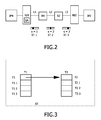
- FIG. 2 shows a block diagram of a connection and a basic slot allocation in a network on chip according to FIG. 1 .
- the connection between the IP block IP 4 and IP 2 is shown.
- This connection is realized by a network interface NI 4 associated to the IP block IP 4 , two routers R 4 , R 2 , and a network interface NI 2 associated to the IP block IP 2 .
- the network interface NI 4 comprises a time slot allocation unit SA.
- the network interface NI 2 , and routers R 2 and R 4 may also comprise a time slot allocation unit SA.
- a first link L 1 is present between the network interface NI 4 and a router R 4
- a second link L 2 is present between the two routers R 4 , R 2
- a third link L 3 is present between the router R 2 and the network interface N 12 .
- the inputs for the slot allocation determination performed by the time slot allocation unit SA are the network topology, like network components, with their interconnection, and the slot table size, and the connection set. For every connection, its paths and its bandwidth, latency, jitter, and/or slot requirements are given.
- a connection consists of at least two channels or connection paths (a request channel from master to slave, and a response channel from slave to master). Each of these channels is set on an individual path, and may comprise different links having different bandwidth, latency, jitter, and/or slot requirements. To provide time related guarantees, slots must be reserved for the links. Different slots can be reserved for different connections by means of TDMA. Data for a connection is then transferred over consecutive links along the connection in consecutive slots.
- FIG. 3 shows a basic representation of the slot tables according to a first embodiment.
- the slot table unit STU can be arranged in the slot allocation unit SA and comprises two slot tables T 1 , T 2 which are nested or interleaved.
- Each of the two slot tables T 1 , T 2 comprises four slots.
- i 2 indicates the slots in the second slot table T 2 .
- the slots in the slot table T 1 , T 2 either relate to a terminal slot or to a nested further slot table.
- the slots of the first slot table T 1 (being at the highest level) are traversed cyclically, i.e. each of the slots in the first slot table T 1 is associated to the same amount of time and therefore bandwidth. If a slot corresponds to a terminal slot, the corresponding channel (or channel entry referring to a channel) (associated to the slot) can access the network. However, if the current slot is associated to a slot table (here the second slot table T 2 ), the slots of the second slot table T 2 are traversed cyclically each time when the first slot table T 1 (being above in the nesting structure) has completed one cycle. Accordingly, the slots within a slot table with a nesting depth of n divide the bandwidth of a single slot at a nesting depth of n ⁇ 1.
- the first slot table T 1 comprises four slots, wherein each of the slots represents 1 ⁇ 4 of the total available link bandwidth.
- the terminal slots T 1 ( 1 ), T 2 ( 2 ) and T 1 ( 3 ) (relating to themselves) are allocated or associated to the channels a, b and c, i.e. each of these channels has 1 ⁇ 4 of the total link bandwidth available.
- the channels d, f and g each have 1/16 of the link bandwidth available.
- the second slot table T 2 is referred for the first time from the first entry T 1 ( 0 ) and the first entry T 2 ( 0 ) of the second table T 2 (the channel d is selected). Then the channels a, b and c are selected sequentially. The next time at the second cycle of the first slot table T 1 , the second slot table T 2 is again referenced from the first entry (T 1 ( 0 )) of the first table T 1 . Now the arbiter selects the second entry T 2 ( 1 ), i.e. channel e of the second table T 2 .
- the slot table unit STU (constituted by the nested table) has the same behaviour as a single slot table. Therefore, the slot allocation can be performed as for a slot table unit without nested slot tables, wherein only an extra constraint on the location of the slot is present. If for example slots are to be allocated with 1/16 of the bandwidth, the slots 0 , 4 , 8 or 12 is needed within the onfolded slot table as depicted above. Furthermore, if slots with 1 ⁇ 4 of the link bandwidth is required, slots need to be periodically (with a period of 4) allocated in the slot table.
- multiple slot points to the same lower level slot table are possible. These slots do not need to be in the same table or even at the same level.
- FIG. 4 shows a representation of a slot table unit STU according to a second embodiment.
- the slot table unit STU comprises five slot tables T 0 , T 1 , T 2 , T 3 and T 4 , which are interconnected in a nested manner.
- the nesting structure is fixed with a physical memory per slot table.
- the memory M is addressed by its address addr and a channel is indicated by M (addr).
- the size of the memory is represented by “size”.
- Each of the slot tables comprises a pointer “parent to-addr” indicating the address at which it is nested from its parent slot table.
- each of the slot tables comprises two inputs, namely active_in and addr_in as well as three outputs, namely active_out, addr_out and channel_id.
- the active_in/active_out indicate the nesting structure, while the addr_in/addr_out in- and outputs correspond to the address within the slot tables.
- the output channel_id corresponds to the ID of the respective channel.
- the slot T 0 ( 0 ) in the first slot table T 0 is associated to the second slot table T 1 .
- the slot T 0 ( 1 ) of the first slot table T 1 is associated to the third slot table T 2 .
- the slot T 2 ( 0 ) is associated to the fourth slot table T 3 .
- the slot T 2 ( 2 ) is associated to the fifth slot table T 4 .
- a table will become active if its parent slot table is active and when the parent slot table points to the nested slot table.
- a single path is present of the active slot table from the route table to a leave table but not necessarily not all the way down to the leave table.
- the active slot tables but the last slot table within the path comprise an output channel_ID of zero. Accordingly, one active slot table with an output channel_ID being not equal to zero is always present.
- the inputs to the slot table units are active_in at addr_in and the outputs are active_out, addr_out and channel_id. Furthermore, the addr_out is set to zero. If the active_out is smaller than or equal to active_in and the addr_in corresponds to the parent_addr and the channel_id is smaller than or equal to the M(addr)*the active_out, then the addr_out corresponds to the addr_out+the active_out in mod size.
- the slot table unit is implemented using a cyclic shift memory. Accordingly, the content of the shift memory is shifted for one location. The data shifted out of the shift memory is shifted in at the other end of the memory. With such a shift memory, the addressing logic required for random access memory can be avoided. Therefore, the architecture of the slot table unit according to the third embodiment corresponds to the architecture of the slot table unit according to the second embodiment.
- the slot table unit according to the third embodiment can be implemented by the following pseudo code:
- the output addr_out is still present, it is not used to address the memory, but for a comparison in the slot tables. Alternatively to shifting the data in the shift memory, this may also be implemented by a memory dedicated to an incremental addressing.
- the memory can be implemented with an additional bit.
- Such an extra or additional bit can indicate whether a slot in a slot table is a leave or terminal slot or a pointer to a further slot table.
- the other bits within such a slot table may correspond to the channel_ID or the slot table ID according to the value of the extra bit.
- the slot table ID can then be used in the child table or nested table to compare with. Accordingly, such a scheme will allow multiple slots referring to the same child table.
- FIG. 5 shows a representation of a slot table unit according to the fifth embodiment.
- the fifth embodiment is based on the second embodiment while only a single random access memory is used.
- the different physical memories per slot table containing the connection IDs are replaced in the slot tables by a vector V indication whether a current slot within the slot table is nested ( 0 ) or not ( 1 ).
- the state, the local addresses of the vector V inside the block correspond to those in the second embodiment of FIG. 4 .
- the single memory is achieved by stacking the slot tables T 0 -T 4 on top of each other in the memory. This is shown on the left hand side of FIG. 6 .
- Each entry within the slot tables T 0 -T 4 corresponds to an address addr from zero to 17.
- the value cumulative_table_size corresponds to the sum of the sizes of the slot tables being embedded in the single memory before the current table.
- the values thereof for the slot tables T 0 -T 4 correspond to 0, 4, 8, 11 and 14, respectively.
- the only slot table with a value of ‘the_address’ being one is the third slot table with a local output address addr_out being one. Accordingly, the address addr equals to nine. This address corresponds to a connection ID of 7.
- the slot table unit may be implemented by the following pseudo code:
- the output address addr_out of the ‘or’ operation corresponds to the address for the single memory.
- the slot table units according to the second to fifth embodiment are based on a fixed structure which is advantageous as it allows a fast computation of the address such that a new connection ID can be computed easily even at a high rate.
- the slot table units are based on a programmable structure of the nesting of the slot tables. For example, if a memory comprises sixteen locations, such memory can be partitioned into two tables of eight slot, four tables of four slots and so on. If the structure of the slot table units is to be programmed, the computing of the addresses in order for addressing the single memory is now more difficult.
- the values of the cumulative_cable_size is hard-wired or coded, and the interconnect between these units is fixed.
- a first re-indexing points to table 1 a second re-indexing points to table 2 etc.
- the pointer is hard-wired.
- the computation of a required address does not have to be performed within a single clock cycle, but within the duration of a slot which may be several clock cycles.
- slot table units can be applied to a system on chip in particular with a network on chip infrastructure.
- a system on chip with a diverse bandwidth requirement and which needs to be implemented at low cost can greatly benefit from the slot table units according to the above embodiments.
- One example of such a system is a audio/video processing within a mobile device.
- TDMA time-division multiple access
- the invention relates to a provision of nested slot tables.
- a table entry may be a slot or may refer to a next or following slot table.
- the bandwidth of an allocated entry in one of the nested tables will depend on the nesting depth of such an entry. Accordingly, a fine granularity can be obtained with only a moderate number of slots required, such that bandwidths can be saved for the same slot table cost or slot table cost can be reduced for the same amount of allocated bandwidth.
Abstract
Description
| time: | ||
| 0 1 2 3 4 5 6 7 8 9 10 11 12 13 14 15 . . . | ||
| channel: | ||
| d a b c e a b c f a b c g a b c . . . |
| SlotTable (parent_addr): | ||
| IN active_in | |
| IN addr_in | |
| OUT active_out | |
| OUT addr_out | |
| OUT channel_id | |
| addr_out=0; | |
| foreach (slot_tick) |
| active_out <=active_in and (addr_in ==parent_addr); | ||
| channel_id <=M(addr) * active_out; | ||
| addr_out = addr_out + active_out (mod size); | ||
| SlotTable (parent_addr): | ||
| IN active_in | |
| IN addr_in | |
| OUT active_out | |
| OUT addr_out | |
| OUT channel_id | |
| addr_out=0 | |
| foreach (slot_tick) |
| active_out<= active_in and (addr_in ==parent_addr); | ||
| channel_id<=M(0) + active:out; | ||
| M <= shift (M); | ||
| M(size-1) <= channel_id; | ||
| addr_out = addr_out + active_out (mod size); | ||
| AddressUnit (parent_addr): | ||
| IN active_in | |
| IN addr_in | |
| OUT active_out | |
| OUT addr_out | |
| OUT the_address | |
| addr_out = 0; | |
| foreach (slot_tick) |
| active_out <= active_in and (addr_in == parent_addr); |
| the_address <= (cumulative_table_size + addr_out) * (v(addr_out) |
| and active_out); |
| addr_out = addr_out + active_out (mod size); | ||
Claims (20)
Applications Claiming Priority (4)
| Application Number | Priority Date | Filing Date | Title |
|---|---|---|---|
| EP05104512.8 | 2005-05-26 | ||
| EP05104512 | 2005-05-26 | ||
| EP05104512 | 2005-05-26 | ||
| PCT/IB2006/051487 WO2006126127A2 (en) | 2005-05-26 | 2006-05-11 | Electronic device and method of communication resource allocation |
Publications (2)
| Publication Number | Publication Date |
|---|---|
| US20080310458A1 US20080310458A1 (en) | 2008-12-18 |
| US7809024B2 true US7809024B2 (en) | 2010-10-05 |
Family
ID=37258890
Family Applications (1)
| Application Number | Title | Priority Date | Filing Date |
|---|---|---|---|
| US11/915,497 Expired - Fee Related US7809024B2 (en) | 2005-05-26 | 2006-05-11 | Electronic device and method of communication resource allocation |
Country Status (6)
| Country | Link |
|---|---|
| US (1) | US7809024B2 (en) |
| EP (1) | EP1889412B1 (en) |
| JP (1) | JP4756158B2 (en) |
| CN (1) | CN101180841B (en) |
| AT (1) | ATE528889T1 (en) |
| WO (1) | WO2006126127A2 (en) |
Cited By (1)
| Publication number | Priority date | Publication date | Assignee | Title |
|---|---|---|---|---|
| TWI464592B (en) * | 2011-08-31 | 2014-12-11 | Intel Corp | Integrating intellectual property (ip) blocks into a processor |
Families Citing this family (15)
| Publication number | Priority date | Publication date | Assignee | Title |
|---|---|---|---|---|
| US8930602B2 (en) | 2011-08-31 | 2015-01-06 | Intel Corporation | Providing adaptive bandwidth allocation for a fixed priority arbiter |
| US8713240B2 (en) | 2011-09-29 | 2014-04-29 | Intel Corporation | Providing multiple decode options for a system-on-chip (SoC) fabric |
| US8775700B2 (en) | 2011-09-29 | 2014-07-08 | Intel Corporation | Issuing requests to a fabric |
| US8929373B2 (en) | 2011-09-29 | 2015-01-06 | Intel Corporation | Sending packets with expanded headers |
| US8874976B2 (en) | 2011-09-29 | 2014-10-28 | Intel Corporation | Providing error handling support to legacy devices |
| US8805926B2 (en) * | 2011-09-29 | 2014-08-12 | Intel Corporation | Common idle state, active state and credit management for an interface |
| US8711875B2 (en) | 2011-09-29 | 2014-04-29 | Intel Corporation | Aggregating completion messages in a sideband interface |
| US8713234B2 (en) | 2011-09-29 | 2014-04-29 | Intel Corporation | Supporting multiple channels of a single interface |
| US9053251B2 (en) | 2011-11-29 | 2015-06-09 | Intel Corporation | Providing a sideband message interface for system on a chip (SoC) |
| US9571402B2 (en) * | 2013-05-03 | 2017-02-14 | Netspeed Systems | Congestion control and QoS in NoC by regulating the injection traffic |
| CN107566074B (en) * | 2016-06-30 | 2019-06-11 | 华为技术有限公司 | The method and transmission equipment of client signal are transmitted in optical transfer network |
| US10666578B2 (en) * | 2016-09-06 | 2020-05-26 | Taiwan Semiconductor Manufacturing Company Limited | Network-on-chip system and a method of generating the same |
| US10911261B2 (en) | 2016-12-19 | 2021-02-02 | Intel Corporation | Method, apparatus and system for hierarchical network on chip routing |
| US10846126B2 (en) | 2016-12-28 | 2020-11-24 | Intel Corporation | Method, apparatus and system for handling non-posted memory write transactions in a fabric |
| US11264361B2 (en) | 2019-06-05 | 2022-03-01 | Invensas Corporation | Network on layer enabled architectures |
Citations (8)
| Publication number | Priority date | Publication date | Assignee | Title |
|---|---|---|---|---|
| US5875309A (en) * | 1997-04-18 | 1999-02-23 | 3Com Corporation | Arbitration system using linked table |
| WO2005099187A1 (en) | 2004-04-05 | 2005-10-20 | Koninklijke Philips Electronics N.V. | Integrated circuit and method for time slot allocation |
| EP1605727A1 (en) | 2004-06-09 | 2005-12-14 | Koninklijke Philips Electronics N.V. | Integrated circuit and method for time slot allocation |
| US7006534B1 (en) * | 1999-03-18 | 2006-02-28 | Fujitsu Limited | Radio communication system and method for calculating transmission timing between a terminal unit and a base station based upon location, distance, or propagation time |
| WO2006051471A1 (en) | 2004-11-09 | 2006-05-18 | Koninklijke Philips Electronics N.V. | Electronic device and method of communication resource allocation |
| WO2006106475A1 (en) | 2005-04-06 | 2006-10-12 | Koninklijke Philips Electronics N. V. | Network-on-chip environment and method for reduction of latency |
| US20070274263A1 (en) * | 2005-02-08 | 2007-11-29 | Hiroyuki Seki | Slot allocation method for use in cellular radio communication system and base station for use in the same system |
| US7443790B2 (en) * | 2000-10-27 | 2008-10-28 | Yt Networks Capital, Llc | System and method for slot deflection routing at optical router/switch |
Family Cites Families (1)
| Publication number | Priority date | Publication date | Assignee | Title |
|---|---|---|---|---|
| US20070010205A1 (en) * | 2003-05-14 | 2007-01-11 | Koninklijke Philips Electronics N.V. | Time-division multiplexing circuit-switching router |
-
2006
- 2006-05-11 CN CN2006800178597A patent/CN101180841B/en not_active Expired - Fee Related
- 2006-05-11 EP EP06744916A patent/EP1889412B1/en active Active
- 2006-05-11 JP JP2008512975A patent/JP4756158B2/en not_active Expired - Fee Related
- 2006-05-11 WO PCT/IB2006/051487 patent/WO2006126127A2/en active Application Filing
- 2006-05-11 AT AT06744916T patent/ATE528889T1/en not_active IP Right Cessation
- 2006-05-11 US US11/915,497 patent/US7809024B2/en not_active Expired - Fee Related
Patent Citations (8)
| Publication number | Priority date | Publication date | Assignee | Title |
|---|---|---|---|---|
| US5875309A (en) * | 1997-04-18 | 1999-02-23 | 3Com Corporation | Arbitration system using linked table |
| US7006534B1 (en) * | 1999-03-18 | 2006-02-28 | Fujitsu Limited | Radio communication system and method for calculating transmission timing between a terminal unit and a base station based upon location, distance, or propagation time |
| US7443790B2 (en) * | 2000-10-27 | 2008-10-28 | Yt Networks Capital, Llc | System and method for slot deflection routing at optical router/switch |
| WO2005099187A1 (en) | 2004-04-05 | 2005-10-20 | Koninklijke Philips Electronics N.V. | Integrated circuit and method for time slot allocation |
| EP1605727A1 (en) | 2004-06-09 | 2005-12-14 | Koninklijke Philips Electronics N.V. | Integrated circuit and method for time slot allocation |
| WO2006051471A1 (en) | 2004-11-09 | 2006-05-18 | Koninklijke Philips Electronics N.V. | Electronic device and method of communication resource allocation |
| US20070274263A1 (en) * | 2005-02-08 | 2007-11-29 | Hiroyuki Seki | Slot allocation method for use in cellular radio communication system and base station for use in the same system |
| WO2006106475A1 (en) | 2005-04-06 | 2006-10-12 | Koninklijke Philips Electronics N. V. | Network-on-chip environment and method for reduction of latency |
Non-Patent Citations (6)
| Title |
|---|
| Gossens, K; et al "A Unified Approach to Constrained Mapping and Routing on Network-on-Chip Architectures" Proceedings of the 3rd IEEE/ACM/IFIP International Conference on Hardware/Software Codesign and System Synthesis, Sep. 2005, pp. 75-80. |
| Libin, Dong; et al "Effect of Scheduling Jitter on End-to-End Delay in TDMA Protocols" Proceedings of the International Conference on Real-Time Computing Systems and Applications, Dec. 2000, pp. 223-230. |
| Marchal P; et al "Spatial Division Multiplexing: A Novel Approach for Guaranteed Throughput on NOCS" Proceedings of the 3rd IEEE/ACM/IFIP International Conference on Hardware/Software Codesign and System Synthesis, Sep. 2005, pp. 81-86. |
| Radulescu, A; et al "Communication Services for Networks on Chip" Proceedings of the International Workshop on Systems, Architectures, Modeling and Simulation, SAMOS, vol. 2, 2002, pp. 275-299. |
| Rijpkema, E; et al "Trade-Offs in the Design of a Router With Both Guaranteed and Best-Effort Services for Networks on Chip" IEEE Proceedings on Computers and Digital Techniques, vol. 150, No. 5, Sep. 22, 2003, pp. 294-302. |
| Sathe, S; et al "Design of a Switching Node (Router) for On-Chip Networks" ASIC, 2003. Proceedings. 5th International Conference, vol. 1, Oct. 2003, pp. 75-78. |
Cited By (2)
| Publication number | Priority date | Publication date | Assignee | Title |
|---|---|---|---|---|
| TWI464592B (en) * | 2011-08-31 | 2014-12-11 | Intel Corp | Integrating intellectual property (ip) blocks into a processor |
| US9021156B2 (en) | 2011-08-31 | 2015-04-28 | Prashanth Nimmala | Integrating intellectual property (IP) blocks into a processor |
Also Published As
| Publication number | Publication date |
|---|---|
| US20080310458A1 (en) | 2008-12-18 |
| JP2008543151A (en) | 2008-11-27 |
| WO2006126127A2 (en) | 2006-11-30 |
| CN101180841A (en) | 2008-05-14 |
| ATE528889T1 (en) | 2011-10-15 |
| EP1889412B1 (en) | 2011-10-12 |
| WO2006126127A3 (en) | 2007-03-29 |
| JP4756158B2 (en) | 2011-08-24 |
| CN101180841B (en) | 2011-11-30 |
| EP1889412A2 (en) | 2008-02-20 |
Similar Documents
| Publication | Publication Date | Title |
|---|---|---|
| US7809024B2 (en) | Electronic device and method of communication resource allocation | |
| US7564865B2 (en) | Weight factor based allocation of time slot to use link in connection path in network on chip IC | |
| US20080232387A1 (en) | Electronic Device and Method of Communication Resource Allocation | |
| EP1759559B1 (en) | Data processing system and method for time slot allocation | |
| US20080186998A1 (en) | Network-On-Chip Environment and Method for Reduction of Latency | |
| US20080205432A1 (en) | Network-On-Chip Environment and Method For Reduction of Latency | |
| EP1552669A1 (en) | Integrated circuit and method for establishing transactions | |
| EP1875681A1 (en) | Electronic device and method for flow control | |
| EP1625757A1 (en) | Time-division multiplexing circuit-switching router | |
| US20080123666A1 (en) | Electronic Device And Method Of Communication Resource Allocation | |
| CN101069434B (en) | Data processing system and method for converting and synchronising data traffic |
Legal Events
| Date | Code | Title | Description |
|---|---|---|---|
| AS | Assignment |
Owner name: NXP B.V., NETHERLANDS Free format text: ASSIGNMENT OF ASSIGNORS INTEREST;ASSIGNORS:RIJPKEMA, EDWIN;DIELISSEN, JOHN;REEL/FRAME:021248/0726;SIGNING DATES FROM 20071017 TO 20071228 Owner name: NXP B.V., NETHERLANDS Free format text: ASSIGNMENT OF ASSIGNORS INTEREST;ASSIGNORS:RIJPKEMA, EDWIN;DIELISSEN, JOHN;SIGNING DATES FROM 20071017 TO 20071228;REEL/FRAME:021248/0726 |
|
| FPAY | Fee payment |
Year of fee payment: 4 |
|
| AS | Assignment |
Owner name: ST-ERICSSON SA, SWITZERLAND Free format text: CHANGE OF NAME;ASSIGNOR:ST WIRELESS SA;REEL/FRAME:033817/0155 Effective date: 20090407 Owner name: ERICSSON MODEMS SA, SWITZERLAND Free format text: ASSIGNMENT OF ASSIGNORS INTEREST;ASSIGNOR:NXP B.V.;REEL/FRAME:033816/0912 Effective date: 20080728 Owner name: ST WIRELESS SA, SWITZERLAND Free format text: ASSIGNMENT OF ASSIGNORS INTEREST;ASSIGNOR:NXP B.V.;REEL/FRAME:033816/0912 Effective date: 20080728 |
|
| AS | Assignment |
Owner name: ST WIRELESS SA, SWITZERLAND Free format text: CORRECTIVE ASSIGNMENT TO CORRECT THE ASSIGNEE PREVIOUSLY RECORDED AT REEL: 33816 FRAME: 0912. ASSIGNOR(S) HEREBY CONFIRMS THE ASSIGNMENT;ASSIGNOR:NXP B.V.;REEL/FRAME:033864/0063 Effective date: 20080728 |
|
| AS | Assignment |
Owner name: ST-ERICSSON SA, EN LIQUIDATION, SWITZERLAND Free format text: CHANGE OF NAME;ASSIGNORS:ST WIRELESS SA;ST-ERICSSON SA;REEL/FRAME:034470/0582 Effective date: 20141113 |
|
| AS | Assignment |
Owner name: MORGAN STANLEY SENIOR FUNDING, INC., MARYLAND Free format text: SECURITY AGREEMENT SUPPLEMENT;ASSIGNOR:NXP B.V.;REEL/FRAME:038017/0058 Effective date: 20160218 |
|
| AS | Assignment |
Owner name: MORGAN STANLEY SENIOR FUNDING, INC., MARYLAND Free format text: CORRECTIVE ASSIGNMENT TO CORRECT THE REMOVE APPLICATION 12092129 PREVIOUSLY RECORDED ON REEL 038017 FRAME 0058. ASSIGNOR(S) HEREBY CONFIRMS THE SECURITY AGREEMENT SUPPLEMENT;ASSIGNOR:NXP B.V.;REEL/FRAME:039361/0212 Effective date: 20160218 |
|
| AS | Assignment |
Owner name: NXP B.V., NETHERLANDS Free format text: PATENT RELEASE;ASSIGNOR:MORGAN STANLEY SENIOR FUNDING, INC.;REEL/FRAME:039707/0471 Effective date: 20160805 |
|
| AS | Assignment |
Owner name: MORGAN STANLEY SENIOR FUNDING, INC., MARYLAND Free format text: CORRECTIVE ASSIGNMENT TO CORRECT THE REMOVE APPLICATION 12681366 PREVIOUSLY RECORDED ON REEL 039361 FRAME 0212. ASSIGNOR(S) HEREBY CONFIRMS THE SECURITY AGREEMENT SUPPLEMENT;ASSIGNOR:NXP B.V.;REEL/FRAME:042762/0145 Effective date: 20160218 Owner name: MORGAN STANLEY SENIOR FUNDING, INC., MARYLAND Free format text: CORRECTIVE ASSIGNMENT TO CORRECT THE REMOVE APPLICATION 12681366 PREVIOUSLY RECORDED ON REEL 038017 FRAME 0058. ASSIGNOR(S) HEREBY CONFIRMS THE SECURITY AGREEMENT SUPPLEMENT;ASSIGNOR:NXP B.V.;REEL/FRAME:042985/0001 Effective date: 20160218 |
|
| FEPP | Fee payment procedure |
Free format text: MAINTENANCE FEE REMINDER MAILED (ORIGINAL EVENT CODE: REM.) |
|
| LAPS | Lapse for failure to pay maintenance fees |
Free format text: PATENT EXPIRED FOR FAILURE TO PAY MAINTENANCE FEES (ORIGINAL EVENT CODE: EXP.); ENTITY STATUS OF PATENT OWNER: LARGE ENTITY |
|
| STCH | Information on status: patent discontinuation |
Free format text: PATENT EXPIRED DUE TO NONPAYMENT OF MAINTENANCE FEES UNDER 37 CFR 1.362 |
|
| FP | Lapsed due to failure to pay maintenance fee |
Effective date: 20181005 |
|
| AS | Assignment |
Owner name: NXP B.V., NETHERLANDS Free format text: RELEASE BY SECURED PARTY;ASSIGNOR:MORGAN STANLEY SENIOR FUNDING, INC.;REEL/FRAME:050745/0001 Effective date: 20190903 |
|
| AS | Assignment |
Owner name: MORGAN STANLEY SENIOR FUNDING, INC., MARYLAND Free format text: CORRECTIVE ASSIGNMENT TO CORRECT THE REMOVE APPLICATION 12298143 PREVIOUSLY RECORDED ON REEL 042762 FRAME 0145. ASSIGNOR(S) HEREBY CONFIRMS THE SECURITY AGREEMENT SUPPLEMENT;ASSIGNOR:NXP B.V.;REEL/FRAME:051145/0184 Effective date: 20160218 Owner name: MORGAN STANLEY SENIOR FUNDING, INC., MARYLAND Free format text: CORRECTIVE ASSIGNMENT TO CORRECT THE REMOVE APPLICATION 12298143 PREVIOUSLY RECORDED ON REEL 039361 FRAME 0212. ASSIGNOR(S) HEREBY CONFIRMS THE SECURITY AGREEMENT SUPPLEMENT;ASSIGNOR:NXP B.V.;REEL/FRAME:051029/0387 Effective date: 20160218 Owner name: MORGAN STANLEY SENIOR FUNDING, INC., MARYLAND Free format text: CORRECTIVE ASSIGNMENT TO CORRECT THE REMOVE APPLICATION 12298143 PREVIOUSLY RECORDED ON REEL 042985 FRAME 0001. ASSIGNOR(S) HEREBY CONFIRMS THE SECURITY AGREEMENT SUPPLEMENT;ASSIGNOR:NXP B.V.;REEL/FRAME:051029/0001 Effective date: 20160218 Owner name: MORGAN STANLEY SENIOR FUNDING, INC., MARYLAND Free format text: CORRECTIVE ASSIGNMENT TO CORRECT THE REMOVE APPLICATION 12298143 PREVIOUSLY RECORDED ON REEL 038017 FRAME 0058. ASSIGNOR(S) HEREBY CONFIRMS THE SECURITY AGREEMENT SUPPLEMENT;ASSIGNOR:NXP B.V.;REEL/FRAME:051030/0001 Effective date: 20160218 Owner name: MORGAN STANLEY SENIOR FUNDING, INC., MARYLAND Free format text: CORRECTIVE ASSIGNMENT TO CORRECT THE REMOVE APPLICATION12298143 PREVIOUSLY RECORDED ON REEL 039361 FRAME 0212. ASSIGNOR(S) HEREBY CONFIRMS THE SECURITY AGREEMENT SUPPLEMENT;ASSIGNOR:NXP B.V.;REEL/FRAME:051029/0387 Effective date: 20160218 Owner name: MORGAN STANLEY SENIOR FUNDING, INC., MARYLAND Free format text: CORRECTIVE ASSIGNMENT TO CORRECT THE REMOVE APPLICATION12298143 PREVIOUSLY RECORDED ON REEL 042985 FRAME 0001. ASSIGNOR(S) HEREBY CONFIRMS THE SECURITY AGREEMENT SUPPLEMENT;ASSIGNOR:NXP B.V.;REEL/FRAME:051029/0001 Effective date: 20160218 Owner name: MORGAN STANLEY SENIOR FUNDING, INC., MARYLAND Free format text: CORRECTIVE ASSIGNMENT TO CORRECT THE REMOVE APPLICATION12298143 PREVIOUSLY RECORDED ON REEL 042762 FRAME 0145. ASSIGNOR(S) HEREBY CONFIRMS THE SECURITY AGREEMENT SUPPLEMENT;ASSIGNOR:NXP B.V.;REEL/FRAME:051145/0184 Effective date: 20160218 |