US7808496B2 - Apparatus for supplying power source - Google Patents
Apparatus for supplying power source Download PDFInfo
- Publication number
- US7808496B2 US7808496B2 US11/430,042 US43004206A US7808496B2 US 7808496 B2 US7808496 B2 US 7808496B2 US 43004206 A US43004206 A US 43004206A US 7808496 B2 US7808496 B2 US 7808496B2
- Authority
- US
- United States
- Prior art keywords
- voltage
- display device
- circuit
- switch
- node
- Prior art date
- Legal status (The legal status is an assumption and is not a legal conclusion. Google has not performed a legal analysis and makes no representation as to the accuracy of the status listed.)
- Active, expires
Links
Images


Classifications
-
- H—ELECTRICITY
- H02—GENERATION; CONVERSION OR DISTRIBUTION OF ELECTRIC POWER
- H02M—APPARATUS FOR CONVERSION BETWEEN AC AND AC, BETWEEN AC AND DC, OR BETWEEN DC AND DC, AND FOR USE WITH MAINS OR SIMILAR POWER SUPPLY SYSTEMS; CONVERSION OF DC OR AC INPUT POWER INTO SURGE OUTPUT POWER; CONTROL OR REGULATION THEREOF
- H02M3/00—Conversion of dc power input into dc power output
- H02M3/02—Conversion of dc power input into dc power output without intermediate conversion into ac
- H02M3/04—Conversion of dc power input into dc power output without intermediate conversion into ac by static converters
- H02M3/10—Conversion of dc power input into dc power output without intermediate conversion into ac by static converters using discharge tubes with control electrode or semiconductor devices with control electrode
- H02M3/145—Conversion of dc power input into dc power output without intermediate conversion into ac by static converters using discharge tubes with control electrode or semiconductor devices with control electrode using devices of a triode or transistor type requiring continuous application of a control signal
- H02M3/155—Conversion of dc power input into dc power output without intermediate conversion into ac by static converters using discharge tubes with control electrode or semiconductor devices with control electrode using devices of a triode or transistor type requiring continuous application of a control signal using semiconductor devices only
- H02M3/156—Conversion of dc power input into dc power output without intermediate conversion into ac by static converters using discharge tubes with control electrode or semiconductor devices with control electrode using devices of a triode or transistor type requiring continuous application of a control signal using semiconductor devices only with automatic control of output voltage or current, e.g. switching regulators
- H02M3/158—Conversion of dc power input into dc power output without intermediate conversion into ac by static converters using discharge tubes with control electrode or semiconductor devices with control electrode using devices of a triode or transistor type requiring continuous application of a control signal using semiconductor devices only with automatic control of output voltage or current, e.g. switching regulators including plural semiconductor devices as final control devices for a single load
-
- G—PHYSICS
- G09—EDUCATION; CRYPTOGRAPHY; DISPLAY; ADVERTISING; SEALS
- G09G—ARRANGEMENTS OR CIRCUITS FOR CONTROL OF INDICATING DEVICES USING STATIC MEANS TO PRESENT VARIABLE INFORMATION
- G09G2330/00—Aspects of power supply; Aspects of display protection and defect management
- G09G2330/02—Details of power systems and of start or stop of display operation
-
- G—PHYSICS
- G09—EDUCATION; CRYPTOGRAPHY; DISPLAY; ADVERTISING; SEALS
- G09G—ARRANGEMENTS OR CIRCUITS FOR CONTROL OF INDICATING DEVICES USING STATIC MEANS TO PRESENT VARIABLE INFORMATION
- G09G3/00—Control arrangements or circuits, of interest only in connection with visual indicators other than cathode-ray tubes
- G09G3/20—Control arrangements or circuits, of interest only in connection with visual indicators other than cathode-ray tubes for presentation of an assembly of a number of characters, e.g. a page, by composing the assembly by combination of individual elements arranged in a matrix no fixed position being assigned to or needed to be assigned to the individual characters or partial characters
- G09G3/22—Control arrangements or circuits, of interest only in connection with visual indicators other than cathode-ray tubes for presentation of an assembly of a number of characters, e.g. a page, by composing the assembly by combination of individual elements arranged in a matrix no fixed position being assigned to or needed to be assigned to the individual characters or partial characters using controlled light sources
- G09G3/30—Control arrangements or circuits, of interest only in connection with visual indicators other than cathode-ray tubes for presentation of an assembly of a number of characters, e.g. a page, by composing the assembly by combination of individual elements arranged in a matrix no fixed position being assigned to or needed to be assigned to the individual characters or partial characters using controlled light sources using electroluminescent panels
- G09G3/32—Control arrangements or circuits, of interest only in connection with visual indicators other than cathode-ray tubes for presentation of an assembly of a number of characters, e.g. a page, by composing the assembly by combination of individual elements arranged in a matrix no fixed position being assigned to or needed to be assigned to the individual characters or partial characters using controlled light sources using electroluminescent panels semiconductive, e.g. using light-emitting diodes [LED]
-
- H—ELECTRICITY
- H02—GENERATION; CONVERSION OR DISTRIBUTION OF ELECTRIC POWER
- H02M—APPARATUS FOR CONVERSION BETWEEN AC AND AC, BETWEEN AC AND DC, OR BETWEEN DC AND DC, AND FOR USE WITH MAINS OR SIMILAR POWER SUPPLY SYSTEMS; CONVERSION OF DC OR AC INPUT POWER INTO SURGE OUTPUT POWER; CONTROL OR REGULATION THEREOF
- H02M1/00—Details of apparatus for conversion
- H02M1/0003—Details of control, feedback or regulation circuits
- H02M1/0025—Arrangements for modifying reference values, feedback values or error values in the control loop of a converter
-
- H—ELECTRICITY
- H02—GENERATION; CONVERSION OR DISTRIBUTION OF ELECTRIC POWER
- H02M—APPARATUS FOR CONVERSION BETWEEN AC AND AC, BETWEEN AC AND DC, OR BETWEEN DC AND DC, AND FOR USE WITH MAINS OR SIMILAR POWER SUPPLY SYSTEMS; CONVERSION OF DC OR AC INPUT POWER INTO SURGE OUTPUT POWER; CONTROL OR REGULATION THEREOF
- H02M1/00—Details of apparatus for conversion
- H02M1/0045—Converters combining the concepts of switch-mode regulation and linear regulation, e.g. linear pre-regulator to switching converter, linear and switching converter in parallel, same converter or same transistor operating either in linear or switching mode
-
- H—ELECTRICITY
- H02—GENERATION; CONVERSION OR DISTRIBUTION OF ELECTRIC POWER
- H02M—APPARATUS FOR CONVERSION BETWEEN AC AND AC, BETWEEN AC AND DC, OR BETWEEN DC AND DC, AND FOR USE WITH MAINS OR SIMILAR POWER SUPPLY SYSTEMS; CONVERSION OF DC OR AC INPUT POWER INTO SURGE OUTPUT POWER; CONTROL OR REGULATION THEREOF
- H02M1/00—Details of apparatus for conversion
- H02M1/0067—Converter structures employing plural converter units, other than for parallel operation of the units on a single load
- H02M1/008—Plural converter units for generating at two or more independent and non-parallel outputs, e.g. systems with plural point of load switching regulators
Definitions
- the present invention relates to an apparatus for supplying power source. More particularly, the present invention relates to an apparatus for supplying power source for providing power source to a first display device and a second display device.
- An apparatus for supplying power source means apparatus for supplying power source required for driving a display device to the display device.
- FIG. 1 is a view illustrating circuitry of a common apparatus for supplying power source.
- the apparatus for supplying power source 100 includes a boosting circuit 106 and a boosted voltage detecting circuit 108 .
- the boosting circuit 106 includes a boosting integrated chip 110 , an inductor L and a diode D.
- the boosting integrated chip 110 boosts a battery voltage outputted from a battery 102 , e.g. voltage of 3.7V up to a predetermined voltage, e.g. 18V. Accordingly, a first node N 1 has the voltage boosted by the boosting circuit 106 , and the voltage of the first node N 1 is provided to the display device 104 .
- the boosted voltage detecting circuit 108 detects the battery voltage boosted by the boosting circuit 106 , i.e. the voltage of the first node N 1 and a voltage of a second node N 2 , and then provides the voltage of the second node N 2 to a feedback terminal FB of the boosting integrated chip 110 .
- the boosted voltage detecting circuit 106 includes resistors R 1 and R 2 and capacitors C 1 and C 2 .
- the capacitors C 1 and C 2 make the voltage of the first node N 1 provided to the display device 104 stabilize.
- the boosting integrated chip 110 adjusts its boosting rate in accordance with the voltage of the second node N 2 provided from the boosted voltage detecting circuit 108 .
- the apparatus for supplying power source 100 provides a predetermined voltage to only one display device 104 .
- a dual panel apparatus such as a mobile terminal and a laptop, etc. employs two display devices, and thus should include two apparatuses for supplying power source for driving the display devices. Accordingly, the size of the dual panel apparatus may be increased.
- An apparatus for supplying power source includes a boosting circuit, a boosted voltage detecting circuit and an output selecting circuit.
- the boosting circuit boosts a battery voltage.
- the boosted voltage detecting circuit detects the boosted battery voltage, and transmits the detection result to the boosting circuit.
- the output selecting circuit is coupled to the boosting circuit and the boosted voltage detecting circuit, and provides selectively the boosted battery voltage to a first display device and a second display device.
- An apparatus for supplying power source includes a boosting circuit, a voltage adjusting circuit and an outputting circuit.
- the boosting circuit boosts a battery voltage.
- the voltage adjusting circuit controls the boosting circuit so that the boosting circuit boosts the battery voltage up to a first voltage or a second voltage.
- the outputting circuit provides the first voltage to a first display device, downs the second voltage, and provides the downed second voltage to a second display device.
- the apparatus for supplying power source provides certain voltage to a first display device and/or a second display device, and thus the size of a dual panel apparatus employing the display devices may be reduced.
- FIG. 1 is a view illustrating circuitry of a common apparatus for supplying power source
- FIG. 2 is a block diagram illustrating an apparatus for supplying power source according to one embodiment of the present invention
- FIG. 3 is a view illustrating a circuitry of the apparatus for supplying power source of FIG. 2 ;
- FIG. 4 is a block diagram illustrating an apparatus for supplying power source according to another embodiment of the present invention.
- FIG. 5 is a view illustrating a circuitry of the apparatus for supplying power source of FIG. 4 according to one embodiment of the present invention.
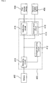
- FIG. 2 is a block diagram illustrating an apparatus for supplying power source according to one embodiment of the present invention.
- the apparatus for supplying power source 200 of the present invention includes a boosting circuit 208 , a boosted voltage detecting circuit 210 and an output selecting circuit 212 .
- the boosting circuit 208 boosts a battery voltage outputted from a battery 202 up to a desired voltage. For example, in case that a voltage of 20V is preset to be provided to a first display device 204 , the boosting circuit 208 boosts the battery voltage, e.g. voltage of 3.7V up to 20V. For another example, in case that a voltage of 18V is preset to be provided to a second display device 206 , the boosting circuit 208 boosts the battery voltage of 3.7V up to 18V.
- the first display device 204 is liquid crystal display
- the second display device 206 is organic electroluminescent device.
- each of the display devices 204 and 206 is organic electroluminescent device.
- the display devices 204 and 206 may be employed as display sections of a mobile terminal.
- the boosted voltage detecting circuit 210 detects the battery voltage boosted by the boosting circuit 208 , and transmits the detection result to the boosting circuit 208 .
- the boosting circuit 208 analyzes the detection result transmitted from the boosted voltage detecting circuit 210 , and adjusts its boosting ratio, e.g. duty ratio in accordance with the analysis.
- a voltage to be provided to the first display device 204 is preset to be 18V.
- the boosting circuit 208 boosts the battery voltage, e.g. voltage of 3.7V up to a voltage of 17.5V.
- the boosted voltage detecting circuit 210 detects the battery voltage boosted up to 17.5V, and transmits the detection result to the boosting circuit 208 .
- the boosting circuit 208 detects that the battery voltage is boosted up to 17.5V through the detection result transmitted from the boosted voltage detecting circuit 210 , and increases its boosting ratio in order to boost the battery voltage up to 18V. For example, if the boosting circuit 208 boosts the battery voltage by using on/off ratio of switch (not shown) included therein, i.e. duty ratio, the boosting circuit 208 boosts its duty ratio in accordance with the detection result transmitted from the boosted voltage detecting circuit 210 . In other words, the boosting circuit 208 boosts the battery voltage up to 18V by adjusting its duty ratio.
- the apparatus 200 of the present invention boosts the battery voltage up to a desired voltage through the above process.
- the output selecting circuit 212 is coupled to the boosting circuit 208 and the boosted voltage detecting circuit 210 , and provides the battery voltage boosted by the boosting circuit 208 to the first display device 204 or the second display device 206 .
- the mobile terminal employs the first display device 204 as main display section, and employs the second display device 206 as sub display section.
- the output selecting circuit 212 of the apparatus 200 of the present invention provides the battery voltage boosted by the boosting circuit 208 to the first display device 204 .
- the output selecting circuit 212 provides the battery voltage boosted by the boosting circuit 208 to the second display device 206 .
- the boosting degree of the battery voltage is determined by the boosting circuit 208 and the boosted voltage detecting circuit 210 . This will be described in detail with reference to accompanying drawings.
- the apparatus for supplying power source 200 of the present invention may provide power source to the first display device 204 or the second display device 206 unlike the apparatus for supplying power source described in Related Art. Accordingly, in case that a dual panel apparatus, e.g. mobile terminal employs the apparatus 200 of the present invention, the apparatus 200 may supply power supply to the first display device 204 and the second display device 206 . As a result, the size of the dual panel apparatus may be reduced.
- FIG. 3 is a view illustrating a circuitry of the apparatus for supplying power source of FIG. 2 according to one embodiment of the present invention.
- the boosting circuit 208 includes a boosting integrated chip 220 activated in accordance with a controlling signal provided from a first signal terminal S 1 , an inductor L and a diode D.
- the boosted voltage detecting circuit 210 is coupled to the boosting circuit 208 , and includes a first resistor R 1 , a second and third resistors R 2 and R 3 , a first switch T 1 and capacitors C 1 and C 2 .
- the resistors R 2 and R 3 are coupled to the first resistor R 1 , and are coupled in parallel each other.
- the output selecting circuit 212 includes a second switch T 2 and an inverter coupled to the first switch T 1 , and a third switch T 3 coupled in serial to the inverter.
- the first switch T 1 is P-MOS transistor
- each of the second and third switches T 2 and T 3 is N-MOS transistor.
- a voltage of 20V is provided to the first display device 204
- a voltage of 18V is provided to the second display device 206 .
- the first switch T 1 is turned off in accordance with a controlling signal provided from a second signal terminal S 2 .
- the second switch T 2 is turned on, and the third switch T 3 is turned off.
- the boosted voltage detecting circuit 210 is made up of resistors R 1 and R 2 coupled in serial.
- the boosted voltage detecting circuit 210 detects a voltage of the third node N 3 .
- the voltage of the third node N 3 is assumed to be 1.5V.
- the boosted voltage detecting circuit 210 detects the voltage of the third node N 3 , e.g. detects the voltage of the third node N 3 of 1.3V corresponding to the voltage of the second node N 2 of 16V.
- the boosted voltage detecting circuit 210 provides the voltage of the third node N 3 of 1.3V to the FB of the boosting integrated chip 220 .
- the boosting integrated chip 220 detects that the battery voltage is not boosted up to a predetermined voltage (18V), and so increases its boosting ratio.
- the second node N 2 has voltage of 18V through the above process, and the voltage of the second node N 2 is provided to the second display device 206 .
- the resistors R 2 and R 3 coupled in parallel are coupled to the first resistor R 1 .
- the second and third resistors R 2 and R 3 are coupled in parallel each other, a resistance formed by the resistors R 2 and R 3 is smaller than that of the second resistor R 2 .
- the voltage of the third node N 3 when the third resistor R 3 is coupled to the second resistor R 2 is smaller than that when the third resistor R 3 is not coupled to the second resistor R 2 .
- the voltage of the third node N 3 when the third resistor R 3 is not coupled to the second resistor R 2 is 1.3V.
- the voltage of the third node N 3 when the third resistor R 3 is coupled to the second resistor R 2 is 1.2V.
- the boosting integrated chip 220 increases its boosting ratio more than boosting ration when the third resistor R 3 is not coupled to the second resistor R 2 , and so the second node N 2 has 20V higher than 18V.
- the voltage of 20V is provided to the first display device 204 .
- the apparatus 200 of the present invention provides selectively voltages having different magnitude to the first display device 204 and the second display device 206 by using the first switch T 1 and the resistors R 2 and R 3 .
- the boosted voltage detecting circuit 210 may be include at least three resistors which are coupled to the first resistor R 1 , and are coupled in parallel one another.
- FIG. 4 is a block diagram illustrating an apparatus for supplying power source according to another embodiment of the present invention.
- the apparatus for supplying power source 400 of the present invention includes a boosting circuit 410 , a voltage adjusting circuit 412 and an outputting circuit 414 .
- the boosting circuit 410 boosts a battery voltage outputted from a battery 402 up to a desired voltage.
- the voltage adjusting circuit 412 adjusts boosting ratio of the boosting circuit 410 so that the boosting circuit 410 boosts the battery voltage up to the desired voltage.
- the outputting circuit 414 provides the battery voltage boosted by the boosting circuit 410 to a first display device 404 and/or a second display device 406 , and has a switching circuit 416 and a voltage down circuit 418 .
- the switching circuit 416 switches couple between the boosting circuit 410 and the first display device 404 , and provides the battery voltage boosted by the boosting circuit 410 to the first display device 404 .
- the voltage down circuit 418 downs the battery voltage boosted by the boosting circuit 410 , and provides the downed voltage to the second display device 406 .
- FIG. 5 is a view illustrating a circuitry of the apparatus for supplying power source of FIG. 4 according to one embodiment of the present invention.
- the boosting circuit 410 is made up of a boosting integrated chip 500 , an inductor L and a first diode D 1 .
- the boosting integrated chip 500 boosts the battery voltage outputted from the battery 402 using switch (not shown) included therein as described below.
- the switch is turned off, and so the battery voltage is stored in the inductor L.
- the switch is turned on, and so charges charged in the inductor L is outputted to a first node N 1 .
- the switch is turned off, and so the battery voltage is stored in the inductor L.
- the switch is turned on, and so charges charged in the inductor L is outputted to the first node N 1 .
- on/off ratio of the switch means duty ratio.
- the second node N 2 has the battery voltage boosted by the boosting circuit 410 .
- the voltage adjusting circuit 412 includes a first capacitor C 1 , a second diode D 2 , a first resistor R 1 , a second resistor R 2 , a third resistor R 3 , a first switch T 1 , a second switch T 2 , a second capacitor C 2 and a third capacitor C 3 .
- the first capacitor C 1 is coupled to the boosting circuit 410
- the second diode D 2 is coupled to the first capacitor C 1 and the boosting integrated chip 500 .
- the first capacitor C 1 and the second diode D 2 make a voltage inputted to FB of the boosting integrated chip 500 , i.e. voltage of a third node N 3 stabilize.
- the first resistor R 1 is coupled to the boosting circuit 410 , and the second resistor R 2 is selectively coupled to the first resistor R 1 .
- the second resistor R 2 is coupled in serial to the first resistor R 1 .
- the first switch T 1 is turned off, the second resistor R 2 is not coupled to the first resistor R 1 .
- the boosting integrated chip 500 has the same boosting ratio, voltage outputted from the boosting circuit 410 may be changed depending on couple of the resistors R 1 and R 2 .
- the boosting circuit 410 may output voltages having different magnitude using the same boosting ratio.
- the third resistor R 3 is coupled in parallel to the second resistor R 2 when the second switch T 2 is turned on in accordance with a controlling signal provided from a third signal terminal S 3 .
- the third resistor R 3 is resistor used for adjusting the boosting ratio of the boosting circuit 410 .
- each of the switches T 1 and T 2 is MOS transistor, preferably N-MOS transistor.
- a fourth resistor R 4 may be coupled between a gate terminal of the first transistor T 1 and a ground in order to protect the first transistor T 1 .
- a fifth resistor R 5 may be coupled between a gate terminal of the second transistor T 2 and the ground so as to protect the second transistor T 2 .
- the second and third capacitors C 2 and C 3 make voltage provided to the display devices 404 and 406 , i.e. voltage of the second node N 2 stabilize.
- the switching circuit 416 includes a third switch T 3 , e.g. MOS transistor switching in accordance with a controlling signal transmitted from a fourth signal terminal S 4 .
- a third switch T 3 e.g. MOS transistor switching in accordance with a controlling signal transmitted from a fourth signal terminal S 4 .
- the voltage down circuit 418 includes an LDO (Low DropOut) regulator 502 for downing the voltage outputted from the boosting circuit 410 , a seventh resistor R 7 coupled between a ground terminal GND and an output voltage adjusting terminal ADJ of the LDO regulator 502 , and an eighth resistor R 8 coupled between the ADJ and the second display device 406 .
- LDO Low DropOut
- the voltage down circuit 418 adjusts the voltage outputted from the boosting circuit 410 inputted to a voltage input terminal VIN of the LDO regulator 502 using the resistors R 7 and R 8 coupled to the ADJ of the LDO regulator 502 .
- the LDO regulator 502 is turned on in accordance with a controlling signal transmitted from a fifth signal terminal S 5 coupled to an enable terminal EN of the LDO regulator 502 , and then the voltage outputted from the boosting circuit 410 is inputted to the LDO regulator 502 .
- the LDO regulator 502 downs the voltage outputted from the boosting circuit 410 to a desired voltage in accordance with the resistors R 7 and R 8 .
- the voltage down circuit 418 may further include a sixth resistor R 6 and a fourth capacitor C 4 .
- the sixth resistor R 6 as full down resistor is coupled between the EN and the ground terminal GND of the LDO regulator 502 , and stabilizes a digital signal inputted to the ground terminal GND of the LDO regulator 502 .
- the fourth capacitor C 4 stabilizes a voltage outputted from the LDO regulator 502 provided to the second display device 406 .
- the switching circuit 416 is turned on, and the LDO regulator 502 is not activated in accordance with a controlling signal transmitted from the fifth signal terminal S 5 . Additionally, when the battery voltage, e.g. voltage of 3.7V is boosted up to 20V, the third node N 3 is assumed to have 9V.
- the first switch T 1 and the second switch T 2 are turned on.
- the voltage adjusting circuit 412 detects that the voltage of the third node N 3 is 7V in accordance with distribution of the resistors R 1 to R 3 .
- the voltage adjusting circuit 412 provides the detected voltage of the third node N 3 to the FB of the boosting integrated chip 500 .
- the boosting integrated chip 500 detects that the battery voltage is not boosted up to a desired voltage (20V) through the detected voltage of the third node N 3 provided from the voltage adjusting circuit 412 . Accordingly, the boosting integrated chip 500 boosts the battery voltage up to the desired voltage (20V) by adjusting its duty ratio.
- the boosted battery voltage of 20V is provided to the first display device 404 through the switching circuit 416 .
- the switching circuit 416 is turned off, and the LDO regulator 502 is activated in accordance with a controlling signal transmitted from the fifth signal terminal S 5 .
- the battery voltage e.g. voltage of 3.7V is boosted up to 18V
- the third node N 3 is assumed to have 9V.
- the first switch T 1 is turned on, and the second switch T 2 are turned off.
- the voltage adjusting circuit 412 detects that the voltage of the third node N 3 is 8V in accordance with distribution of the resistors R 1 and R 2 .
- the voltage adjusting circuit 412 provides the detected voltage of the third node N 3 to the FB of the boosting integrated chip 500 .
- the boosting integrated chip 500 detects that the battery voltage is not boosted up to a desired voltage (18V) through the voltage of the third node N 3 provided from the voltage adjusting circuit 412 . Accordingly, the boosting integrated chip 500 boosts the battery voltage up to the desired voltage (18V) by adjusting its duty ratio.
- the boosted battery voltage of 18V is downed by the voltage down circuit 418 , and then the downed voltage is provided to the second display device 406 .
- the resistors R 2 and R 3 are coupled in parallel each other.
- the first switch T 1 is turned on and the second switch T 2 is turned off, only the second resistor R 2 of the resistors R 2 and R 3 is activated. Therefore, when the battery voltage boosted by the boosting circuit 410 is 16V, the third node N 3 has 7V in the first embodiment, but has 8V in the second embodiment.
- the battery voltage boosted by the boosting circuit 410 is 20V in the first embodiment, but is 18V in the second embodiment. Accordingly, the boosted battery voltage of 20V is provided to the first display device 404 .
- the boosted battery voltage of 18V is downed by the voltage down circuit 418 , and then the downed voltage is provided to the second display device 406 .
- the boosted battery voltage is 20V. Then, the boosted battery voltage of 20V is downed by the voltage adjusting circuit 418 , and the downed voltage is provided to the second display device 406 .
- power consumption of the apparatus 400 when the second switch T 2 is turned on is higher than that of the apparatus 400 when the second switch T 2 is turned off.
- the second switch T 2 is turned off, and so power consumption of the apparatus 400 may be reduced.
- the apparatus 400 of the present invention reduces its power consumption by properly combining the resistors R 1 to R 3 .
- a first voltage is provided to the first display device 400 .
- the second display device 406 is sub display section of the dual panel apparatus, a second voltage smaller than the first voltage is downed so as to enhance power consumption of the apparatus 400 , and then the downed voltage is provided to the second display device 406 .
- the switching circuit 416 is turned on, and the LDO regulator 502 is activated in accordance with a controlling signal transmitted from the fifth signal terminal S 5 .
- the battery voltage boosted by the boosting circuit 410 e.g. voltage of 20V is provided to the first display device 404 .
- the boosted battery voltage of 20V is downed by the voltage down circuit 418 , and then the downed voltage is provided to the second display device 406 .
- the apparatus for supplying power source 400 of the present invention may provide corresponding power source to the first display device 404 and/or the second display device 406 of the dual panel apparatus.
Abstract
Description
Claims (6)
Priority Applications (1)
| Application Number | Priority Date | Filing Date | Title |
|---|---|---|---|
| US12/879,407 US8149231B2 (en) | 2005-05-12 | 2010-09-10 | Apparatus for supplying power source |
Applications Claiming Priority (4)
| Application Number | Priority Date | Filing Date | Title |
|---|---|---|---|
| KR10-2005-0039599 | 2005-05-12 | ||
| KR1020050039599A KR100682991B1 (en) | 2005-05-12 | 2005-05-12 | Method of supplying power source and apparatus for performing the same |
| KR10-2005-0086708 | 2005-09-16 | ||
| KR20050086708 | 2005-09-16 |
Related Child Applications (1)
| Application Number | Title | Priority Date | Filing Date |
|---|---|---|---|
| US12/879,407 Division US8149231B2 (en) | 2005-05-12 | 2010-09-10 | Apparatus for supplying power source |
Publications (2)
| Publication Number | Publication Date |
|---|---|
| US20060267973A1 US20060267973A1 (en) | 2006-11-30 |
| US7808496B2 true US7808496B2 (en) | 2010-10-05 |
Family
ID=37462773
Family Applications (2)
| Application Number | Title | Priority Date | Filing Date |
|---|---|---|---|
| US11/430,042 Active 2028-09-01 US7808496B2 (en) | 2005-05-12 | 2006-05-09 | Apparatus for supplying power source |
| US12/879,407 Active US8149231B2 (en) | 2005-05-12 | 2010-09-10 | Apparatus for supplying power source |
Family Applications After (1)
| Application Number | Title | Priority Date | Filing Date |
|---|---|---|---|
| US12/879,407 Active US8149231B2 (en) | 2005-05-12 | 2010-09-10 | Apparatus for supplying power source |
Country Status (2)
| Country | Link |
|---|---|
| US (2) | US7808496B2 (en) |
| TW (2) | TWI327805B (en) |
Cited By (1)
| Publication number | Priority date | Publication date | Assignee | Title |
|---|---|---|---|---|
| US20070269168A1 (en) * | 2006-05-16 | 2007-11-22 | Jung-Kook Park | Organic light emitting display device and power supply unit for the same |
Families Citing this family (6)
| Publication number | Priority date | Publication date | Assignee | Title |
|---|---|---|---|---|
| FR2924628B1 (en) * | 2007-12-11 | 2010-01-22 | Renault Sas | DEVICE FOR SUPPLYING A SET OF MEMBRANE ACTUATORS OF ELECTRO-ACTIVE POLYMER |
| CN102801188B (en) | 2011-05-26 | 2015-05-20 | 华硕电脑股份有限公司 | Power management method and electronic system using the same |
| KR101940220B1 (en) * | 2012-10-23 | 2019-01-18 | 엘지디스플레이 주식회사 | Display Device Including Power Control Unit And Method Of Driving The Same |
| CN110010099B (en) * | 2019-04-29 | 2020-08-04 | 深圳市华星光电技术有限公司 | Voltage stabilizing circuit, control method and display device |
| JP7344249B2 (en) * | 2021-06-14 | 2023-09-13 | レノボ・シンガポール・プライベート・リミテッド | power supply device |
| US11893931B2 (en) | 2021-11-05 | 2024-02-06 | Samsung Electronics Co., Ltd. | Electronic device including power supply circuit |
Citations (5)
| Publication number | Priority date | Publication date | Assignee | Title |
|---|---|---|---|---|
| US4338531A (en) * | 1980-09-15 | 1982-07-06 | Corporate Equipment Company | Slide wire device simulator circuit and method |
| US6369558B2 (en) * | 2000-06-23 | 2002-04-09 | Rohm Co., Ltd. | Switching regulator |
| WO2003038981A1 (en) | 2001-10-31 | 2003-05-08 | Mobility Electronics, Inc. | Dual input ac and dc power supply having a programmable dc output utilizing a secondary buck converter |
| US20040252096A1 (en) * | 2003-05-21 | 2004-12-16 | Der-Jiunn Wang | Dual panel display backlight power controller chip for handheld apparatus |
| US20050116655A1 (en) * | 2003-11-28 | 2005-06-02 | Tohoku Pioneer Corporation | Self light emitting display device |
Family Cites Families (6)
| Publication number | Priority date | Publication date | Assignee | Title |
|---|---|---|---|---|
| US6313828B1 (en) * | 1996-11-12 | 2001-11-06 | Carlos Landetta Chombo | Electronic book |
| US6035423A (en) * | 1997-12-31 | 2000-03-07 | Network Associates, Inc. | Method and system for providing automated updating and upgrading of antivirus applications using a computer network |
| US6349311B1 (en) * | 1999-02-01 | 2002-02-19 | Symantec Corporation | Storage of reverse delta updates |
| US6671757B1 (en) * | 2000-01-26 | 2003-12-30 | Fusionone, Inc. | Data transfer and synchronization system |
| US6470329B1 (en) * | 2000-07-11 | 2002-10-22 | Sun Microsystems, Inc. | One-way hash functions for distributed data synchronization |
| TWI266106B (en) * | 2002-08-09 | 2006-11-11 | Sanyo Electric Co | Display device with a plurality of display panels |
-
2006
- 2006-05-05 TW TW095116041A patent/TWI327805B/en active
- 2006-05-05 TW TW098130817A patent/TWI408542B/en active
- 2006-05-09 US US11/430,042 patent/US7808496B2/en active Active
-
2010
- 2010-09-10 US US12/879,407 patent/US8149231B2/en active Active
Patent Citations (6)
| Publication number | Priority date | Publication date | Assignee | Title |
|---|---|---|---|---|
| US4338531A (en) * | 1980-09-15 | 1982-07-06 | Corporate Equipment Company | Slide wire device simulator circuit and method |
| US6369558B2 (en) * | 2000-06-23 | 2002-04-09 | Rohm Co., Ltd. | Switching regulator |
| WO2003038981A1 (en) | 2001-10-31 | 2003-05-08 | Mobility Electronics, Inc. | Dual input ac and dc power supply having a programmable dc output utilizing a secondary buck converter |
| CN1541439A (en) | 2001-10-31 | 2004-10-27 | ƶ��� | dual input Ac and DC power supply having programmable DC output utilizing secondary buck converter |
| US20040252096A1 (en) * | 2003-05-21 | 2004-12-16 | Der-Jiunn Wang | Dual panel display backlight power controller chip for handheld apparatus |
| US20050116655A1 (en) * | 2003-11-28 | 2005-06-02 | Tohoku Pioneer Corporation | Self light emitting display device |
Cited By (2)
| Publication number | Priority date | Publication date | Assignee | Title |
|---|---|---|---|---|
| US20070269168A1 (en) * | 2006-05-16 | 2007-11-22 | Jung-Kook Park | Organic light emitting display device and power supply unit for the same |
| US8379008B2 (en) * | 2006-05-16 | 2013-02-19 | Samsung Display Co., Ltd. | Organic light emitting display device and power supply unit for the same |
Also Published As
| Publication number | Publication date |
|---|---|
| TWI408542B (en) | 2013-09-11 |
| US8149231B2 (en) | 2012-04-03 |
| US20060267973A1 (en) | 2006-11-30 |
| TW201005501A (en) | 2010-02-01 |
| US20110037756A1 (en) | 2011-02-17 |
| TWI327805B (en) | 2010-07-21 |
| TW200701589A (en) | 2007-01-01 |
Similar Documents
| Publication | Publication Date | Title |
|---|---|---|
| US7889190B2 (en) | Apparatus for supplying power source | |
| US11823604B2 (en) | DC-DC converter and display device including the same | |
| US8149231B2 (en) | Apparatus for supplying power source | |
| US7414330B2 (en) | Power switch device | |
| US7505290B2 (en) | Power supply apparatus including charge-pump type step-up circuit having different discharging time constants | |
| US6949892B2 (en) | Light emitting element drive device and electronic device light emitting element | |
| US7683553B2 (en) | LED current control circuits and methods | |
| US20080122291A1 (en) | Switching Power Supply Control Circuit, Switching Power Supply Device and Electronic Apparatus Employing the Same | |
| US20140139111A1 (en) | Load driving apparatus related to light emitting diodes | |
| US8884545B2 (en) | LED driving system and driving method thereof | |
| KR101968342B1 (en) | Power supply system for display panel | |
| CN111613185A (en) | Light emitting element driving device, light emitting element driving system, and light emitting system | |
| US7990373B2 (en) | Power supply circuit for liquid crystal display device and liquid crystal display device using the same | |
| US20080290734A1 (en) | Switching pulse generating circuit and regulator using the same | |
| JP2007236126A (en) | Power system and electronic apparatus employing the same | |
| US10152937B2 (en) | Semiconductor device, power supply circuit, and liquid crystal display device | |
| US9536488B2 (en) | Gamma voltage supply circuit and method and power management IC | |
| US20080111807A1 (en) | Multi-output switching power supply having voltage limiting circuit | |
| KR100696563B1 (en) | Apparatus for supplying power source | |
| CN1866705B (en) | Apparatus for supplying power source | |
| US7498794B1 (en) | Method and system for sensing current independently of variations in operating conditions | |
| US7821323B2 (en) | Bias circuit for a switching power supply |
Legal Events
| Date | Code | Title | Description |
|---|---|---|---|
| AS | Assignment |
Owner name: LG ELECTRONICS INC., KOREA, REPUBLIC OF Free format text: ASSIGNMENT OF ASSIGNORS INTEREST;ASSIGNORS:WOO, KYOUNG DON;KIM, HAK SU;REEL/FRAME:017863/0809 Effective date: 20060328 |
|
| AS | Assignment |
Owner name: LG DISPLAY CO., LTD., KOREA, REPUBLIC OF Free format text: ASSIGNMENT OF ASSIGNORS INTEREST;ASSIGNOR:LG ELECTRONICS INC.;REEL/FRAME:020845/0783 Effective date: 20080404 Owner name: LG DISPLAY CO., LTD.,KOREA, REPUBLIC OF Free format text: ASSIGNMENT OF ASSIGNORS INTEREST;ASSIGNOR:LG ELECTRONICS INC.;REEL/FRAME:020845/0783 Effective date: 20080404 |
|
| STCF | Information on status: patent grant |
Free format text: PATENTED CASE |
|
| FEPP | Fee payment procedure |
Free format text: PAYOR NUMBER ASSIGNED (ORIGINAL EVENT CODE: ASPN); ENTITY STATUS OF PATENT OWNER: LARGE ENTITY |
|
| FPAY | Fee payment |
Year of fee payment: 4 |
|
| MAFP | Maintenance fee payment |
Free format text: PAYMENT OF MAINTENANCE FEE, 8TH YEAR, LARGE ENTITY (ORIGINAL EVENT CODE: M1552) Year of fee payment: 8 |
|
| MAFP | Maintenance fee payment |
Free format text: PAYMENT OF MAINTENANCE FEE, 12TH YEAR, LARGE ENTITY (ORIGINAL EVENT CODE: M1553); ENTITY STATUS OF PATENT OWNER: LARGE ENTITY Year of fee payment: 12 |