US7808087B2 - Leadframe IC packages having top and bottom integrated heat spreaders - Google Patents
Leadframe IC packages having top and bottom integrated heat spreaders Download PDFInfo
- Publication number
- US7808087B2 US7808087B2 US11/527,573 US52757306A US7808087B2 US 7808087 B2 US7808087 B2 US 7808087B2 US 52757306 A US52757306 A US 52757306A US 7808087 B2 US7808087 B2 US 7808087B2
- Authority
- US
- United States
- Prior art keywords
- cap
- package
- die
- leadframe
- leads
- Prior art date
- Legal status (The legal status is an assumption and is not a legal conclusion. Google has not performed a legal analysis and makes no representation as to the accuracy of the status listed.)
- Active, expires
Links
Images


Classifications
-
- H—ELECTRICITY
- H01—ELECTRIC ELEMENTS
- H01L—SEMICONDUCTOR DEVICES NOT COVERED BY CLASS H10
- H01L23/00—Details of semiconductor or other solid state devices
- H01L23/34—Arrangements for cooling, heating, ventilating or temperature compensation ; Temperature sensing arrangements
- H01L23/42—Fillings or auxiliary members in containers or encapsulations selected or arranged to facilitate heating or cooling
- H01L23/433—Auxiliary members in containers characterised by their shape, e.g. pistons
- H01L23/4334—Auxiliary members in encapsulations
-
- H—ELECTRICITY
- H01—ELECTRIC ELEMENTS
- H01L—SEMICONDUCTOR DEVICES NOT COVERED BY CLASS H10
- H01L23/00—Details of semiconductor or other solid state devices
- H01L23/48—Arrangements for conducting electric current to or from the solid state body in operation, e.g. leads, terminal arrangements ; Selection of materials therefor
-
- H—ELECTRICITY
- H01—ELECTRIC ELEMENTS
- H01L—SEMICONDUCTOR DEVICES NOT COVERED BY CLASS H10
- H01L23/00—Details of semiconductor or other solid state devices
- H01L23/28—Encapsulations, e.g. encapsulating layers, coatings, e.g. for protection
-
- H—ELECTRICITY
- H01—ELECTRIC ELEMENTS
- H01L—SEMICONDUCTOR DEVICES NOT COVERED BY CLASS H10
- H01L23/00—Details of semiconductor or other solid state devices
- H01L23/48—Arrangements for conducting electric current to or from the solid state body in operation, e.g. leads, terminal arrangements ; Selection of materials therefor
- H01L23/488—Arrangements for conducting electric current to or from the solid state body in operation, e.g. leads, terminal arrangements ; Selection of materials therefor consisting of soldered or bonded constructions
- H01L23/495—Lead-frames or other flat leads
- H01L23/49537—Plurality of lead frames mounted in one device
-
- H—ELECTRICITY
- H01—ELECTRIC ELEMENTS
- H01L—SEMICONDUCTOR DEVICES NOT COVERED BY CLASS H10
- H01L23/00—Details of semiconductor or other solid state devices
- H01L23/48—Arrangements for conducting electric current to or from the solid state body in operation, e.g. leads, terminal arrangements ; Selection of materials therefor
- H01L23/488—Arrangements for conducting electric current to or from the solid state body in operation, e.g. leads, terminal arrangements ; Selection of materials therefor consisting of soldered or bonded constructions
- H01L23/495—Lead-frames or other flat leads
- H01L23/49541—Geometry of the lead-frame
- H01L23/49558—Insulating layers on lead frames, e.g. bridging members
-
- H—ELECTRICITY
- H01—ELECTRIC ELEMENTS
- H01L—SEMICONDUCTOR DEVICES NOT COVERED BY CLASS H10
- H01L23/00—Details of semiconductor or other solid state devices
- H01L23/48—Arrangements for conducting electric current to or from the solid state body in operation, e.g. leads, terminal arrangements ; Selection of materials therefor
- H01L23/488—Arrangements for conducting electric current to or from the solid state body in operation, e.g. leads, terminal arrangements ; Selection of materials therefor consisting of soldered or bonded constructions
- H01L23/495—Lead-frames or other flat leads
- H01L23/49568—Lead-frames or other flat leads specifically adapted to facilitate heat dissipation
-
- H—ELECTRICITY
- H01—ELECTRIC ELEMENTS
- H01L—SEMICONDUCTOR DEVICES NOT COVERED BY CLASS H10
- H01L23/00—Details of semiconductor or other solid state devices
- H01L23/552—Protection against radiation, e.g. light or electromagnetic waves
-
- H—ELECTRICITY
- H01—ELECTRIC ELEMENTS
- H01L—SEMICONDUCTOR DEVICES NOT COVERED BY CLASS H10
- H01L24/00—Arrangements for connecting or disconnecting semiconductor or solid-state bodies; Methods or apparatus related thereto
- H01L24/93—Batch processes
- H01L24/95—Batch processes at chip-level, i.e. with connecting carried out on a plurality of singulated devices, i.e. on diced chips
- H01L24/97—Batch processes at chip-level, i.e. with connecting carried out on a plurality of singulated devices, i.e. on diced chips the devices being connected to a common substrate, e.g. interposer, said common substrate being separable into individual assemblies after connecting
-
- H—ELECTRICITY
- H01—ELECTRIC ELEMENTS
- H01L—SEMICONDUCTOR DEVICES NOT COVERED BY CLASS H10
- H01L2224/00—Indexing scheme for arrangements for connecting or disconnecting semiconductor or solid-state bodies and methods related thereto as covered by H01L24/00
- H01L2224/01—Means for bonding being attached to, or being formed on, the surface to be connected, e.g. chip-to-package, die-attach, "first-level" interconnects; Manufacturing methods related thereto
- H01L2224/26—Layer connectors, e.g. plate connectors, solder or adhesive layers; Manufacturing methods related thereto
- H01L2224/31—Structure, shape, material or disposition of the layer connectors after the connecting process
- H01L2224/32—Structure, shape, material or disposition of the layer connectors after the connecting process of an individual layer connector
- H01L2224/321—Disposition
- H01L2224/32151—Disposition the layer connector connecting between a semiconductor or solid-state body and an item not being a semiconductor or solid-state body, e.g. chip-to-substrate, chip-to-passive
- H01L2224/32221—Disposition the layer connector connecting between a semiconductor or solid-state body and an item not being a semiconductor or solid-state body, e.g. chip-to-substrate, chip-to-passive the body and the item being stacked
- H01L2224/32225—Disposition the layer connector connecting between a semiconductor or solid-state body and an item not being a semiconductor or solid-state body, e.g. chip-to-substrate, chip-to-passive the body and the item being stacked the item being non-metallic, e.g. insulating substrate with or without metallisation
-
- H—ELECTRICITY
- H01—ELECTRIC ELEMENTS
- H01L—SEMICONDUCTOR DEVICES NOT COVERED BY CLASS H10
- H01L2224/00—Indexing scheme for arrangements for connecting or disconnecting semiconductor or solid-state bodies and methods related thereto as covered by H01L24/00
- H01L2224/01—Means for bonding being attached to, or being formed on, the surface to be connected, e.g. chip-to-package, die-attach, "first-level" interconnects; Manufacturing methods related thereto
- H01L2224/26—Layer connectors, e.g. plate connectors, solder or adhesive layers; Manufacturing methods related thereto
- H01L2224/31—Structure, shape, material or disposition of the layer connectors after the connecting process
- H01L2224/32—Structure, shape, material or disposition of the layer connectors after the connecting process of an individual layer connector
- H01L2224/321—Disposition
- H01L2224/32151—Disposition the layer connector connecting between a semiconductor or solid-state body and an item not being a semiconductor or solid-state body, e.g. chip-to-substrate, chip-to-passive
- H01L2224/32221—Disposition the layer connector connecting between a semiconductor or solid-state body and an item not being a semiconductor or solid-state body, e.g. chip-to-substrate, chip-to-passive the body and the item being stacked
- H01L2224/32245—Disposition the layer connector connecting between a semiconductor or solid-state body and an item not being a semiconductor or solid-state body, e.g. chip-to-substrate, chip-to-passive the body and the item being stacked the item being metallic
-
- H—ELECTRICITY
- H01—ELECTRIC ELEMENTS
- H01L—SEMICONDUCTOR DEVICES NOT COVERED BY CLASS H10
- H01L2224/00—Indexing scheme for arrangements for connecting or disconnecting semiconductor or solid-state bodies and methods related thereto as covered by H01L24/00
- H01L2224/01—Means for bonding being attached to, or being formed on, the surface to be connected, e.g. chip-to-package, die-attach, "first-level" interconnects; Manufacturing methods related thereto
- H01L2224/42—Wire connectors; Manufacturing methods related thereto
- H01L2224/47—Structure, shape, material or disposition of the wire connectors after the connecting process
- H01L2224/48—Structure, shape, material or disposition of the wire connectors after the connecting process of an individual wire connector
- H01L2224/4805—Shape
- H01L2224/4809—Loop shape
- H01L2224/48091—Arched
-
- H—ELECTRICITY
- H01—ELECTRIC ELEMENTS
- H01L—SEMICONDUCTOR DEVICES NOT COVERED BY CLASS H10
- H01L2224/00—Indexing scheme for arrangements for connecting or disconnecting semiconductor or solid-state bodies and methods related thereto as covered by H01L24/00
- H01L2224/01—Means for bonding being attached to, or being formed on, the surface to be connected, e.g. chip-to-package, die-attach, "first-level" interconnects; Manufacturing methods related thereto
- H01L2224/42—Wire connectors; Manufacturing methods related thereto
- H01L2224/47—Structure, shape, material or disposition of the wire connectors after the connecting process
- H01L2224/48—Structure, shape, material or disposition of the wire connectors after the connecting process of an individual wire connector
- H01L2224/481—Disposition
- H01L2224/48151—Connecting between a semiconductor or solid-state body and an item not being a semiconductor or solid-state body, e.g. chip-to-substrate, chip-to-passive
- H01L2224/48221—Connecting between a semiconductor or solid-state body and an item not being a semiconductor or solid-state body, e.g. chip-to-substrate, chip-to-passive the body and the item being stacked
- H01L2224/48225—Connecting between a semiconductor or solid-state body and an item not being a semiconductor or solid-state body, e.g. chip-to-substrate, chip-to-passive the body and the item being stacked the item being non-metallic, e.g. insulating substrate with or without metallisation
- H01L2224/48227—Connecting between a semiconductor or solid-state body and an item not being a semiconductor or solid-state body, e.g. chip-to-substrate, chip-to-passive the body and the item being stacked the item being non-metallic, e.g. insulating substrate with or without metallisation connecting the wire to a bond pad of the item
-
- H—ELECTRICITY
- H01—ELECTRIC ELEMENTS
- H01L—SEMICONDUCTOR DEVICES NOT COVERED BY CLASS H10
- H01L2224/00—Indexing scheme for arrangements for connecting or disconnecting semiconductor or solid-state bodies and methods related thereto as covered by H01L24/00
- H01L2224/01—Means for bonding being attached to, or being formed on, the surface to be connected, e.g. chip-to-package, die-attach, "first-level" interconnects; Manufacturing methods related thereto
- H01L2224/42—Wire connectors; Manufacturing methods related thereto
- H01L2224/47—Structure, shape, material or disposition of the wire connectors after the connecting process
- H01L2224/48—Structure, shape, material or disposition of the wire connectors after the connecting process of an individual wire connector
- H01L2224/481—Disposition
- H01L2224/48151—Connecting between a semiconductor or solid-state body and an item not being a semiconductor or solid-state body, e.g. chip-to-substrate, chip-to-passive
- H01L2224/48221—Connecting between a semiconductor or solid-state body and an item not being a semiconductor or solid-state body, e.g. chip-to-substrate, chip-to-passive the body and the item being stacked
- H01L2224/48245—Connecting between a semiconductor or solid-state body and an item not being a semiconductor or solid-state body, e.g. chip-to-substrate, chip-to-passive the body and the item being stacked the item being metallic
- H01L2224/48247—Connecting between a semiconductor or solid-state body and an item not being a semiconductor or solid-state body, e.g. chip-to-substrate, chip-to-passive the body and the item being stacked the item being metallic connecting the wire to a bond pad of the item
-
- H—ELECTRICITY
- H01—ELECTRIC ELEMENTS
- H01L—SEMICONDUCTOR DEVICES NOT COVERED BY CLASS H10
- H01L2224/00—Indexing scheme for arrangements for connecting or disconnecting semiconductor or solid-state bodies and methods related thereto as covered by H01L24/00
- H01L2224/01—Means for bonding being attached to, or being formed on, the surface to be connected, e.g. chip-to-package, die-attach, "first-level" interconnects; Manufacturing methods related thereto
- H01L2224/42—Wire connectors; Manufacturing methods related thereto
- H01L2224/47—Structure, shape, material or disposition of the wire connectors after the connecting process
- H01L2224/48—Structure, shape, material or disposition of the wire connectors after the connecting process of an individual wire connector
- H01L2224/481—Disposition
- H01L2224/48151—Connecting between a semiconductor or solid-state body and an item not being a semiconductor or solid-state body, e.g. chip-to-substrate, chip-to-passive
- H01L2224/48221—Connecting between a semiconductor or solid-state body and an item not being a semiconductor or solid-state body, e.g. chip-to-substrate, chip-to-passive the body and the item being stacked
- H01L2224/48245—Connecting between a semiconductor or solid-state body and an item not being a semiconductor or solid-state body, e.g. chip-to-substrate, chip-to-passive the body and the item being stacked the item being metallic
- H01L2224/48257—Connecting between a semiconductor or solid-state body and an item not being a semiconductor or solid-state body, e.g. chip-to-substrate, chip-to-passive the body and the item being stacked the item being metallic connecting the wire to a die pad of the item
-
- H—ELECTRICITY
- H01—ELECTRIC ELEMENTS
- H01L—SEMICONDUCTOR DEVICES NOT COVERED BY CLASS H10
- H01L2224/00—Indexing scheme for arrangements for connecting or disconnecting semiconductor or solid-state bodies and methods related thereto as covered by H01L24/00
- H01L2224/01—Means for bonding being attached to, or being formed on, the surface to be connected, e.g. chip-to-package, die-attach, "first-level" interconnects; Manufacturing methods related thereto
- H01L2224/42—Wire connectors; Manufacturing methods related thereto
- H01L2224/47—Structure, shape, material or disposition of the wire connectors after the connecting process
- H01L2224/49—Structure, shape, material or disposition of the wire connectors after the connecting process of a plurality of wire connectors
- H01L2224/491—Disposition
- H01L2224/49105—Connecting at different heights
- H01L2224/49109—Connecting at different heights outside the semiconductor or solid-state body
-
- H—ELECTRICITY
- H01—ELECTRIC ELEMENTS
- H01L—SEMICONDUCTOR DEVICES NOT COVERED BY CLASS H10
- H01L2224/00—Indexing scheme for arrangements for connecting or disconnecting semiconductor or solid-state bodies and methods related thereto as covered by H01L24/00
- H01L2224/01—Means for bonding being attached to, or being formed on, the surface to be connected, e.g. chip-to-package, die-attach, "first-level" interconnects; Manufacturing methods related thereto
- H01L2224/42—Wire connectors; Manufacturing methods related thereto
- H01L2224/47—Structure, shape, material or disposition of the wire connectors after the connecting process
- H01L2224/49—Structure, shape, material or disposition of the wire connectors after the connecting process of a plurality of wire connectors
- H01L2224/491—Disposition
- H01L2224/4912—Layout
- H01L2224/49171—Fan-out arrangements
-
- H—ELECTRICITY
- H01—ELECTRIC ELEMENTS
- H01L—SEMICONDUCTOR DEVICES NOT COVERED BY CLASS H10
- H01L2224/00—Indexing scheme for arrangements for connecting or disconnecting semiconductor or solid-state bodies and methods related thereto as covered by H01L24/00
- H01L2224/73—Means for bonding being of different types provided for in two or more of groups H01L2224/10, H01L2224/18, H01L2224/26, H01L2224/34, H01L2224/42, H01L2224/50, H01L2224/63, H01L2224/71
- H01L2224/732—Location after the connecting process
- H01L2224/73251—Location after the connecting process on different surfaces
- H01L2224/73265—Layer and wire connectors
-
- H—ELECTRICITY
- H01—ELECTRIC ELEMENTS
- H01L—SEMICONDUCTOR DEVICES NOT COVERED BY CLASS H10
- H01L2224/00—Indexing scheme for arrangements for connecting or disconnecting semiconductor or solid-state bodies and methods related thereto as covered by H01L24/00
- H01L2224/93—Batch processes
- H01L2224/95—Batch processes at chip-level, i.e. with connecting carried out on a plurality of singulated devices, i.e. on diced chips
- H01L2224/97—Batch processes at chip-level, i.e. with connecting carried out on a plurality of singulated devices, i.e. on diced chips the devices being connected to a common substrate, e.g. interposer, said common substrate being separable into individual assemblies after connecting
-
- H—ELECTRICITY
- H01—ELECTRIC ELEMENTS
- H01L—SEMICONDUCTOR DEVICES NOT COVERED BY CLASS H10
- H01L24/00—Arrangements for connecting or disconnecting semiconductor or solid-state bodies; Methods or apparatus related thereto
- H01L24/01—Means for bonding being attached to, or being formed on, the surface to be connected, e.g. chip-to-package, die-attach, "first-level" interconnects; Manufacturing methods related thereto
- H01L24/42—Wire connectors; Manufacturing methods related thereto
- H01L24/47—Structure, shape, material or disposition of the wire connectors after the connecting process
- H01L24/48—Structure, shape, material or disposition of the wire connectors after the connecting process of an individual wire connector
-
- H—ELECTRICITY
- H01—ELECTRIC ELEMENTS
- H01L—SEMICONDUCTOR DEVICES NOT COVERED BY CLASS H10
- H01L24/00—Arrangements for connecting or disconnecting semiconductor or solid-state bodies; Methods or apparatus related thereto
- H01L24/01—Means for bonding being attached to, or being formed on, the surface to be connected, e.g. chip-to-package, die-attach, "first-level" interconnects; Manufacturing methods related thereto
- H01L24/42—Wire connectors; Manufacturing methods related thereto
- H01L24/47—Structure, shape, material or disposition of the wire connectors after the connecting process
- H01L24/49—Structure, shape, material or disposition of the wire connectors after the connecting process of a plurality of wire connectors
-
- H—ELECTRICITY
- H01—ELECTRIC ELEMENTS
- H01L—SEMICONDUCTOR DEVICES NOT COVERED BY CLASS H10
- H01L24/00—Arrangements for connecting or disconnecting semiconductor or solid-state bodies; Methods or apparatus related thereto
- H01L24/73—Means for bonding being of different types provided for in two or more of groups H01L24/10, H01L24/18, H01L24/26, H01L24/34, H01L24/42, H01L24/50, H01L24/63, H01L24/71
-
- H—ELECTRICITY
- H01—ELECTRIC ELEMENTS
- H01L—SEMICONDUCTOR DEVICES NOT COVERED BY CLASS H10
- H01L2924/00—Indexing scheme for arrangements or methods for connecting or disconnecting semiconductor or solid-state bodies as covered by H01L24/00
- H01L2924/0001—Technical content checked by a classifier
- H01L2924/00014—Technical content checked by a classifier the subject-matter covered by the group, the symbol of which is combined with the symbol of this group, being disclosed without further technical details
-
- H—ELECTRICITY
- H01—ELECTRIC ELEMENTS
- H01L—SEMICONDUCTOR DEVICES NOT COVERED BY CLASS H10
- H01L2924/00—Indexing scheme for arrangements or methods for connecting or disconnecting semiconductor or solid-state bodies as covered by H01L24/00
- H01L2924/01—Chemical elements
- H01L2924/01005—Boron [B]
-
- H—ELECTRICITY
- H01—ELECTRIC ELEMENTS
- H01L—SEMICONDUCTOR DEVICES NOT COVERED BY CLASS H10
- H01L2924/00—Indexing scheme for arrangements or methods for connecting or disconnecting semiconductor or solid-state bodies as covered by H01L24/00
- H01L2924/01—Chemical elements
- H01L2924/01006—Carbon [C]
-
- H—ELECTRICITY
- H01—ELECTRIC ELEMENTS
- H01L—SEMICONDUCTOR DEVICES NOT COVERED BY CLASS H10
- H01L2924/00—Indexing scheme for arrangements or methods for connecting or disconnecting semiconductor or solid-state bodies as covered by H01L24/00
- H01L2924/01—Chemical elements
- H01L2924/0101—Neon [Ne]
-
- H—ELECTRICITY
- H01—ELECTRIC ELEMENTS
- H01L—SEMICONDUCTOR DEVICES NOT COVERED BY CLASS H10
- H01L2924/00—Indexing scheme for arrangements or methods for connecting or disconnecting semiconductor or solid-state bodies as covered by H01L24/00
- H01L2924/01—Chemical elements
- H01L2924/01013—Aluminum [Al]
-
- H—ELECTRICITY
- H01—ELECTRIC ELEMENTS
- H01L—SEMICONDUCTOR DEVICES NOT COVERED BY CLASS H10
- H01L2924/00—Indexing scheme for arrangements or methods for connecting or disconnecting semiconductor or solid-state bodies as covered by H01L24/00
- H01L2924/01—Chemical elements
- H01L2924/01018—Argon [Ar]
-
- H—ELECTRICITY
- H01—ELECTRIC ELEMENTS
- H01L—SEMICONDUCTOR DEVICES NOT COVERED BY CLASS H10
- H01L2924/00—Indexing scheme for arrangements or methods for connecting or disconnecting semiconductor or solid-state bodies as covered by H01L24/00
- H01L2924/01—Chemical elements
- H01L2924/01019—Potassium [K]
-
- H—ELECTRICITY
- H01—ELECTRIC ELEMENTS
- H01L—SEMICONDUCTOR DEVICES NOT COVERED BY CLASS H10
- H01L2924/00—Indexing scheme for arrangements or methods for connecting or disconnecting semiconductor or solid-state bodies as covered by H01L24/00
- H01L2924/01—Chemical elements
- H01L2924/01029—Copper [Cu]
-
- H—ELECTRICITY
- H01—ELECTRIC ELEMENTS
- H01L—SEMICONDUCTOR DEVICES NOT COVERED BY CLASS H10
- H01L2924/00—Indexing scheme for arrangements or methods for connecting or disconnecting semiconductor or solid-state bodies as covered by H01L24/00
- H01L2924/01—Chemical elements
- H01L2924/01033—Arsenic [As]
-
- H—ELECTRICITY
- H01—ELECTRIC ELEMENTS
- H01L—SEMICONDUCTOR DEVICES NOT COVERED BY CLASS H10
- H01L2924/00—Indexing scheme for arrangements or methods for connecting or disconnecting semiconductor or solid-state bodies as covered by H01L24/00
- H01L2924/01—Chemical elements
- H01L2924/01074—Tungsten [W]
-
- H—ELECTRICITY
- H01—ELECTRIC ELEMENTS
- H01L—SEMICONDUCTOR DEVICES NOT COVERED BY CLASS H10
- H01L2924/00—Indexing scheme for arrangements or methods for connecting or disconnecting semiconductor or solid-state bodies as covered by H01L24/00
- H01L2924/01—Chemical elements
- H01L2924/01078—Platinum [Pt]
-
- H—ELECTRICITY
- H01—ELECTRIC ELEMENTS
- H01L—SEMICONDUCTOR DEVICES NOT COVERED BY CLASS H10
- H01L2924/00—Indexing scheme for arrangements or methods for connecting or disconnecting semiconductor or solid-state bodies as covered by H01L24/00
- H01L2924/01—Chemical elements
- H01L2924/01082—Lead [Pb]
-
- H—ELECTRICITY
- H01—ELECTRIC ELEMENTS
- H01L—SEMICONDUCTOR DEVICES NOT COVERED BY CLASS H10
- H01L2924/00—Indexing scheme for arrangements or methods for connecting or disconnecting semiconductor or solid-state bodies as covered by H01L24/00
- H01L2924/06—Polymers
- H01L2924/078—Adhesive characteristics other than chemical
- H01L2924/07802—Adhesive characteristics other than chemical not being an ohmic electrical conductor
-
- H—ELECTRICITY
- H01—ELECTRIC ELEMENTS
- H01L—SEMICONDUCTOR DEVICES NOT COVERED BY CLASS H10
- H01L2924/00—Indexing scheme for arrangements or methods for connecting or disconnecting semiconductor or solid-state bodies as covered by H01L24/00
- H01L2924/10—Details of semiconductor or other solid state devices to be connected
- H01L2924/11—Device type
- H01L2924/14—Integrated circuits
-
- H—ELECTRICITY
- H01—ELECTRIC ELEMENTS
- H01L—SEMICONDUCTOR DEVICES NOT COVERED BY CLASS H10
- H01L2924/00—Indexing scheme for arrangements or methods for connecting or disconnecting semiconductor or solid-state bodies as covered by H01L24/00
- H01L2924/15—Details of package parts other than the semiconductor or other solid state devices to be connected
- H01L2924/151—Die mounting substrate
- H01L2924/153—Connection portion
- H01L2924/1531—Connection portion the connection portion being formed only on the surface of the substrate opposite to the die mounting surface
- H01L2924/15311—Connection portion the connection portion being formed only on the surface of the substrate opposite to the die mounting surface being a ball array, e.g. BGA
-
- H—ELECTRICITY
- H01—ELECTRIC ELEMENTS
- H01L—SEMICONDUCTOR DEVICES NOT COVERED BY CLASS H10
- H01L2924/00—Indexing scheme for arrangements or methods for connecting or disconnecting semiconductor or solid-state bodies as covered by H01L24/00
- H01L2924/15—Details of package parts other than the semiconductor or other solid state devices to be connected
- H01L2924/151—Die mounting substrate
- H01L2924/156—Material
- H01L2924/157—Material with a principal constituent of the material being a metal or a metalloid, e.g. boron [B], silicon [Si], germanium [Ge], arsenic [As], antimony [Sb], tellurium [Te] and polonium [Po], and alloys thereof
- H01L2924/15738—Material with a principal constituent of the material being a metal or a metalloid, e.g. boron [B], silicon [Si], germanium [Ge], arsenic [As], antimony [Sb], tellurium [Te] and polonium [Po], and alloys thereof the principal constituent melting at a temperature of greater than or equal to 950 C and less than 1550 C
- H01L2924/15747—Copper [Cu] as principal constituent
-
- H—ELECTRICITY
- H01—ELECTRIC ELEMENTS
- H01L—SEMICONDUCTOR DEVICES NOT COVERED BY CLASS H10
- H01L2924/00—Indexing scheme for arrangements or methods for connecting or disconnecting semiconductor or solid-state bodies as covered by H01L24/00
- H01L2924/15—Details of package parts other than the semiconductor or other solid state devices to be connected
- H01L2924/181—Encapsulation
-
- H—ELECTRICITY
- H01—ELECTRIC ELEMENTS
- H01L—SEMICONDUCTOR DEVICES NOT COVERED BY CLASS H10
- H01L2924/00—Indexing scheme for arrangements or methods for connecting or disconnecting semiconductor or solid-state bodies as covered by H01L24/00
- H01L2924/19—Details of hybrid assemblies other than the semiconductor or other solid state devices to be connected
- H01L2924/191—Disposition
- H01L2924/19101—Disposition of discrete passive components
- H01L2924/19107—Disposition of discrete passive components off-chip wires
-
- H—ELECTRICITY
- H01—ELECTRIC ELEMENTS
- H01L—SEMICONDUCTOR DEVICES NOT COVERED BY CLASS H10
- H01L2924/00—Indexing scheme for arrangements or methods for connecting or disconnecting semiconductor or solid-state bodies as covered by H01L24/00
- H01L2924/30—Technical effects
- H01L2924/301—Electrical effects
- H01L2924/30105—Capacitance
-
- H—ELECTRICITY
- H01—ELECTRIC ELEMENTS
- H01L—SEMICONDUCTOR DEVICES NOT COVERED BY CLASS H10
- H01L2924/00—Indexing scheme for arrangements or methods for connecting or disconnecting semiconductor or solid-state bodies as covered by H01L24/00
- H01L2924/30—Technical effects
- H01L2924/301—Electrical effects
- H01L2924/30107—Inductance
-
- H—ELECTRICITY
- H01—ELECTRIC ELEMENTS
- H01L—SEMICONDUCTOR DEVICES NOT COVERED BY CLASS H10
- H01L2924/00—Indexing scheme for arrangements or methods for connecting or disconnecting semiconductor or solid-state bodies as covered by H01L24/00
- H01L2924/30—Technical effects
- H01L2924/301—Electrical effects
- H01L2924/3025—Electromagnetic shielding
-
- H—ELECTRICITY
- H01—ELECTRIC ELEMENTS
- H01L—SEMICONDUCTOR DEVICES NOT COVERED BY CLASS H10
- H01L2924/00—Indexing scheme for arrangements or methods for connecting or disconnecting semiconductor or solid-state bodies as covered by H01L24/00
- H01L2924/30—Technical effects
- H01L2924/35—Mechanical effects
- H01L2924/351—Thermal stress
Definitions
- the invention relates generally to the field of integrated circuit (IC) device packaging technology and, more particularly to thermal enhancement and electromagnetic interference (EMI) shielding in IC device leadframe packages.
- IC integrated circuit
- EMI electromagnetic interference
- Integrated circuit semiconductor chips or dies are typically mounted in or on a package that is attached to a printed circuit board (PCB).
- PCB printed circuit board
- Leadframes are widely used in IC packages as a carrier for the IC die and as an interconnection mechanism between the die and the electrical circuits of the PCB.
- Various leadframe packages have been developed and package family outlines have been standardized by the Electronic Industries Alliance (EIA), the Joint Electron Device Engineering Council (JEDEC), and the Electronic Industries Alliance of Japan (EIAJ).
- the present invention is directed to methods and apparatus for improved thermal performance and EMI shielding in IC packages.
- a leadframe IC device package includes first and second heat spreader caps (“caps”) having opposing first and second surfaces.
- a first portion of the second surface of the first cap has a cavity formed therein.
- a planar second portion of the second surface of the first cap is coupled to a first surface of a leadframe.
- the leadframe includes a die attach pad (DAP), a plurality of leads, and a plurality of tie bars coupled to the DAP.
- At least one IC die is mounted to the die attach pad on the first surface of the leadframe.
- the second cap is attached to a second surface of the leadframe such that the leadframe is between the first and second caps, one of which is nearer to the printed circuit board.
- the first and second caps and the leadframe form an enclosure structure that substantially encloses the IC die(s).
- an IC device package is assembled.
- a leadframe is formed.
- At least one IC die is attached to a die attach pad portion of a first surface of the leadframe.
- Wire bonds are coupled between the IC die and the leadframe.
- First and second caps are attached to the opposing first and second surfaces of the leadframe.
- the first and second caps and leadframe form an enclosure structure that substantially encloses the IC die.
- the enclosure structure maybe filled with an encapsulating material to encapsulate at least the IC die or may be filled with inert gases like neon.
- a perimeter support ring portion of the leadframe is trimmed. Portions of the leads are bent to form shoulder bends, to aid coupling of ends of the leads to a circuit board.
- the enclosure structure spreads heat from the IC die(s) during operation. Furthermore, the enclosure structure shields EMI emanating from the IC die(s) and EMI radiating toward the IC die(s) from outside the package.
- FIG. 1 illustrates a typical conventional plastic quad flat package (PQFP).
- FIG. 2 illustrates example heat dissipation paths in and from a typical PQFP.
- FIGS. 3A-3D illustrate example ball grid array (BGA) integrated circuit (IC) packages.
- FIGS. 4A-4B illustrate example leadframe IC packages.
- FIGS. 5A-5E show examples of heat spreader caps (caps) according to embodiments of the invention.
- FIGS. 6A-6C show plan views of examples of leadframes according to embodiments of the invention.
- FIGS. 7A-7M show cross-sectional views of examples of leadframe IC packages, according to embodiments of the invention.
- FIGS. 8A-8E show plan views of examples of leadframe IC packages undergoing assembly, according to embodiments of the invention.
- FIGS. 9A-9D show side views of examples of leadframe IC packages undergoing assembly, according to embodiments of the invention.
- FIGS. 10A and 10B show flowcharts illustrating example embodiments for assembling leadframe IC packages, according to embodiments of the invention.
- FIGS. 11A-11C illustrate some ways of implementing a seal ring.
- FIGS. 12A and 12B show horizontal and top views respectively of an inverted cup design for a cap.
- FIGS. 13A and 13B show horizontal and top views respectively of a cap with contact stands with fused leads.
- an IC die is mounted to a die attach pad (DAP) in the center of a leadframe that includes leads along its peripheral.
- DAP die attach pad
- the package is configured in a die-up configuration. In another embodiment, the package is configured in a die-down configuration.
- metal heat spreaders are coupled (e.g. electrically, structurally, and/or thermally connected) to the leadframe to form an enclosure structure.
- the coupling may be effected with or without the use of a thermally and/or electrically conductive adhesive, such as solder or epoxy with metal particles or flakes.
- the caps are coupled to the leadframe tie bars.
- the leadframe tie bars may be widened or fused to leads of the leadframe.
- the caps are directly coupled to the leads.
- the caps are coupled to the DAP.
- the caps may be coupled with any combination of DAP, leads, and tie bars.
- tabs on the caps mate with matching receptacles on the leadframe to improve coupling and overall structural strength. Wire bonds may be used to electrically connect die to leads of the leadframe and/or to the DAP.
- the enclosure structure formed by the two caps and a leadframe approximate an equipotential surface, or Faraday Cage, surrounding the die and corresponding interconnections.
- the enclosure structure material is also a very good conductor of heat and is relatively rigid (e.g., copper or copper alloy such as C194, C151, C7025, or EFTEC/64T).
- the enclosure structure may provide improved EMI shielding, improved heat transfer from the one or more die, enhanced rigidity of the package, and improved environmental (e.g., mechanical shock, vibration, impact, stress, temperature, moisture, corrosion, etc.) protection.
- the die and the wirebonds are encapsulated in an encapsulating material, such as a molding compound, which provides environmental protection.
- the encapsulating material may also completely cover the caps. In other embodiments, the caps are partially covered, or are not covered by the encapsulating material.
- the die and the wirebonds are encapsulated in the enclosure structure, as described above.
- the cavity thus formed is filled with an inert gas such as neon to provide environmental protection.
- one or both of the metal caps is coupled with an external heat sink, to further enhance the thermal performance of the package.
- references in the specification to “one embodiment”, “an embodiment”, “an example embodiment”, etc. indicate that the embodiment described may include a particular feature, structure, or characteristic, but every embodiment may not necessarily include the particular feature, structure, or characteristic. Moreover, such phrases are not necessarily referring to the same embodiment. Further, when a particular feature, structure, or characteristic is described in connection with an embodiment, it is submitted that it is within the knowledge of one skilled in the art to effect such feature, structure, or characteristic in connection with other embodiments whether or not explicitly described.
- FIG. 1 shows a cross-sectional view of a plastic quad flat package (PQFP) 100 .
- An IC die 150 is attached with thermally and/or electrically conductive adhesive 170 to a die attach pad (DAP) 140 portion of a typically copper or copper alloy leadframe 110 .
- Wirebonds 130 form electrical interconnections between die 150 , DAP, and leadframe leads 180 .
- IC die 150 and wirebonds 130 are molded in encapsulating material 120 for environmental protection, which is typically plastic.
- Leads 180 (if any) can be straight or bent and extend from one or more sides of package 100 . Different families of leadframe packages are further discussed in C. A. Happer, Electronic Packaging and Interconnection Handbook, 3 rd edition, McGraw-Hill, New York, pp. 7.61-7.67, 2000, which is incorporated by reference herein in its entirety.
- Plastic molding compound encapsulated leadframe packages 100 commonly exhibit poor thermal performance.
- DAP is typically separated from leadframe leads 180 that extend beyond encapsulating material 120 .
- Heat dissipation paths in and from plastic quad flat pack (PQFP) package 100 are shown in FIG. 2 .
- Heat generated on the active surface of die 150 is conducted via paths 210 into encapsulating material 120 and leadframe 110 .
- Leadframe 110 conducts some heat into a circuit board 160 to which package 100 is attached.
- Encapsulating material 120 transfers heat to the environment through convection path 220 and radiation path 230 .
- Typical encapsulating materials 120 have a low thermal conductivity value, such as around or between 0.2 ⁇ 0.9 W/m ⁇ K. Therefore, the temperature of die 150 must rise to a relatively high value to transfer the heat generated during operation through encapsulating material 120 .
- leadframe packages 100 commonly exhibit poor electromagnetic interference (EMI) shielding.
- EMI electromagnetic interference
- a change in the electrical current carried by a conductor results in the radiation of electromagnetic waves. Such waves propagate through space at the speed of light, and when not wanted, are called EMI.
- a relatively slow change in the electrical current causes a small amount of electromagnetic radiation with a long wavelength and a low frequency.
- a relatively rapid change in the electrical current causes a large amount of radiation with a short wavelength and a high frequency.
- the unwanted high frequency electromagnetic radiation is sometimes called radio-frequency interference (RFI), but in the interest of brevity, this application refers to all unwanted electromagnetic radiation as EMI, regardless of frequency.
- RFID radio-frequency interference
- IC die 150 are more susceptible to higher frequency EMI. Because higher frequencies are more energetic, they may cause larger voltage swings in the metal traces on an IC die. Because modem IC gates are small in size, they operate with a low signal voltage. Thus, signal line voltage swings caused by high-frequency EMI may cause a change in logic state and may result in timing and logic failures in electronic devices.
- Encapsulating materials 120 are typically transparent to electromagnetic radiation. Referring to FIG. 1 , the electromagnetic radiation generated by die 150 will escape from package 100 and potentially interfere with the operation of nearby components. Conversely, EMI from nearby components will enter package 100 and may interfere with the operation of die 150 .
- FIG. 3A illustrates a ball grid array (BGA) package having improved performance.
- FIG. 3A shows a cross-sectional view of a BGA package 300 with an IC die 150 mounted on a printed circuit substrate 310 , encapsulated by a encapsulating material 120 , and electrically connected to PCB 160 through solder balls 330 .
- BGA package 300 includes a drop-in heat spreader 320 to promote dissipation of heat within encapsulating material 120 .
- EMI generated outside BGA package 300 can penetrate printed circuit substrate 310 and interfere with the operation of IC die 150 .
- EMI generated by IC die 150 can escape BGA package 300 through trace metal openings or gaps in printed circuit substrate 310 .
- FIG. 3B illustrates a cross-sectional view of a BGA package 302 , similar to BGA package 300 , but with a differently configured heat spreader 325 .
- BGA package 302 suffers from the same thermal and electromagnetic shielding deficiencies as BGA package 300 .
- An encapsulating material 120 and a printed circuit substrate 310 may trap heat generated by an IC die 150 within BGA package 302 .
- EMI generated inside of BGA package by die 150 may penetrate printed circuit substrate 310 , escape package 302 , and interfere with the operation of other devices. Conversely, EMI originating outside of BGA package 302 may penetrate printed circuit substrate 310 and interfere with the operation of die 150 .
- FIG. 3C illustrates a cross-sectional view of a BGA package 304 , which provides a thermal and electrical connection between an IC die 150 and PCB 160 through a heat slug 360 .
- IC die 150 is directly attached to a top surface of a stiffener 340 .
- a heat slug 360 is attached to a bottom surface of stiffener 340 and has a surface that is configured to be mounted to PCB 160 .
- BGA package 304 promotes heat dissipation from IC die 150 to PCB 160 , on which BGA package 304 is mounted.
- Heat slug 360 acts as a thermal and electric connection for heat and current flow from metal stiffener 340 to PCB 160 .
- Stiffener 340 and heat slug 360 can both be metal.
- Stiffener 340 can be connected to the ground pad on die 150 through a wirebond 130 . Although the grounded metal stiffener 340 could prevent penetration of some EMI, the entire top surface of die 150 is exposed to EMI from above.
- FIG. 3D shows a cross-sectional view of a BGA package 306 , which incorporates a metal stiffener 340 and a metal cap 350 .
- a package similar to package 306 refer to U.S. App. Publ. No. 20050280127, titled “Apparatus And Method For Thermal And Electromagnetic Interference (EMI) Shielding Enhancement In Die-Up Array Packages,” filed Apr. 23, 2004, which is herein incorporated by reference in its entirety.
- a die 150 is located inside of an enclosure formed by metal stiffener 340 and metal cap 350 .
- Metal stiffener 340 is coupled (e.g., electrically, thermally, and/or structurally connected) to metal cap 350 to provide improved EMI shielding, thermal performance, and environmental protection.
- FIG. 4A illustrates a “leadframe”-type package 400 .
- a metal shield 410 is integrated into a die-down leadframe package 400 .
- a top portion of leadframe package 400 is covered with an electrically grounded laminated metal shield 410 .
- EMI can enter or exit through a bottom of the leadframe package 400 , and a ground plane 420 is required on the PCB 430 .
- a sufficiently sized gap between ground plane 420 and metal shield 410 may permit EMI to enter and exit leadframe package 400 .
- FIG. 4B illustrates a leadframe package 405 .
- Package 405 incorporates a shield box 450 within leadframe package 402 , completely encapsulated by encapsulating material 120 .
- IC die 150 is mounted inside shield box 450 .
- Shield box 450 is attached to leadframe 110 and electrically grounded.
- Shield box 450 has a dielectric inner layer and an electrically conductive outer layer of metallic foil.
- Package 405 suffers from the same thermal deficiencies as prior leadframe packages, such as package 100 shown in FIG. 1 .
- a first cap and a second cap are incorporated in an IC package.
- Example structures for the first and second caps are described in this section. These structures are described for illustrative purposes, and are not intended to be limiting. Furthermore, the caps may have sizes and/or proportions other than those described herein. Still further, elements of the cap structures described herein can be combined in any manner.
- FIG. 5A illustrates a cross sectional view of a cap 510 .
- FIG. 5B illustrates a bottom view of cap 510 in accordance with an embodiment of the present invention.
- Cap 510 is an example of the first and second caps that may be incorporated into IC packages.
- Caps 510 may be incorporated into various integrated circuit packages, such as shown in FIGS. 7A-7I , which are described in detail below.
- the packages may incorporate leadframes, such as shown in FIGS. 6A-6C , which are described in detail below.
- cap 510 has a top portion 590 , sidewall portion 592 , and a rim 594 extending around a bottom periphery of the cap 510 .
- Sidewall portion 592 couples (e.g., electrically, structurally, and thermally) top portion 590 to rim 594 .
- sidewall portion 592 is angled outward from top portion 590 .
- FIG. SA illustrates a planar top portion 590
- top portion 590 can be non-planar (e.g., curved, concave, convex, hemispherical, or other shapes).
- sidewall portion 592 may be perpendicular to or angled inward from top portion 590 .
- sidewall portion 592 is not limited to a linear cross-section and may employ other cross-sectional shapes such as convex inward and outward as would be understood by one skilled in the art.
- Cap 510 further has a first surface 580 and a second surface 585 .
- Second surface 585 forms an upper surface of a cavity 570 in a bottom portion of cap 510 .
- Rim 594 surrounds cavity 570 .
- Cavity 570 is shown in FIG. 5A as having a trapezoidal cross section, but may have other shapes (e.g., square, rectangular, irregular, etc.).
- FIG. 5B illustrates second surface 585 having a circular shape, second surface 585 may have other shapes.
- cap 510 may have various shapes such as round, rectangular, square, elliptical, oval, or any other shape.
- a bottom surface of rim 594 has one or more protruding tabs 515 a - e.
- Tabs 515 a - e may have any shape.
- FIGS. 5A and 5B show a frustum tab 515 a, a conical tab 515 b, a pair 517 of conical tabs 515 c and 515 d, and an oblong shaped tab 515 e.
- Cap 510 is not limited to the shapes, sizes, locations, or numbers of tabs 515 shown. Cap 510 may also have zero or more tabs of any shape, of any size, in any locations.
- the outer periphery dimension of cap 510 is preferably the same size as the periphery (e.g., see FIG. 7C ) or smaller than the periphery (see FIG. 7A ) of the leadframe's “shoulder bends” to facilitate visual inspection of lead interconnect on the circuit board.
- the outer periphery dimension of cap 510 extends beyond the periphery of the leadframe's “shoulder bends” leading to a gap 788 as shown in FIG. 7C .
- the outer periphery of cap 510 is preferably smaller than the dimension of the leadframe inner support ring support ring 630 (e.g., see FIGS. 6A and 8C , further described below). Inner support ring 630 is also called a dam bar.
- cap 510 is illustrated as having a particular size, other sizes may be used, as would be understood by persons skilled in the relevant art(s).
- cap 510 may be configured to mount an external heat sink (e.g., see FIG. 7F , further described below).
- cap 510 may be configured to be thermally and/or electrically connected to a circuit board (e.g., see FIGS. 7G and 7H , further described below).
- the circuit board can be any type of circuit board such as a printed circuit board (PCB), a printed wire board (PVVB), etc. as would be understood by someone skilled in the art.
- Cap 510 may be made of a thermally conductive material and/or an electrically conductive material, such as a metal.
- the material for cap 510 may include copper, a copper alloy, (e.g., C194, C151, C7025, or EFTEC/64T), aluminum, an aluminum alloy, ferromagnetic materials, laminated copper or iron, etc.
- Other metals and combinations of metals/alloys, or other thermally and electrically conductive materials e.g., ceramics, metallized plastics, laminated metal foils on plastic or ceramic, etc.
- Cap 510 and the leadframe may be made of the same material or different materials.
- cap 510 and the leadframe are made of the same material, or materials having the same coefficient of thermal expansion, structural integrity may be improved, such as reducing thermal stress on the die (sandwiched between the cap and the leadframe).
- cap 510 may have any thickness, depending on the particular application. For example, cap 510 may have a thickness of 0.1 to 0.5 mm. Alternatively, cap 510 may have a thickness of less than 1.0 mm.
- the bottom surfaces or portions of the bottom surface of rim 594 may be coated or laminated with a layer of dielectric material (e.g. solder mask, dielectric film etc.). In this manner, the shorting of leads after package assembly may be prevented.
- dielectric material e.g. solder mask, dielectric film etc.
- cap 510 may have openings through the first surface 580 and the second surface 585 .
- FIGS. 5C and 5 D show example caps 510 having openings or slots 520 formed in sidewall portions 592 , according to embodiments of the present invention.
- FIGS. 5C and 5D illustrate slots 520 in sidewall portion 592 as rectangular or trapezoidal, slots 520 can have other shapes.
- cap 510 may have holes/openings 530 in top portion 590 as illustrated in FIG. 5E , according to an example embodiment of the present invention.
- Cap 510 may have any number of holes.
- holes 530 can have any shape.
- holes 530 and slots 520 allow the flow of encapsulating material 120 into cavity 570 during a manufacturing process. Additionally or alternatively, slots 520 and holes 530 may release pressure buildup (during or after manufacture) occurring in cavity 570 . Because smaller holes 530 and slots 520 may require a higher pressure to flow or inject encapsulating material 120 into cavity 570 , larger holes 530 and slots 520 may be desirable from a manufacturing perspective. However, in an embodiment, cap 510 may require the size of holes 530 and slots 520 to be limited to reduce EMI penetration. In an embodiment, a hole 530 or slot 520 diameter is in the range of 0.5-3.0 mm.
- a diameter 1.5 mm may be used to shield against EMI having a highest harmonic frequency of about 10 GHz.
- An outer surface of cap 510 may be completely or partially encapsulated in encapsulating material 120 , or may have no encapsulating material 120 covering it.
- Example embodiments for leadframe structures are described in this section. Further embodiments will become apparent to persons having skill in the relevant art(s) from the teachings herein. Elements of the leadframe embodiments described herein can be combined in any manner in leadframes.
- FIGS. 6A-6C illustrate various leadframe structures, according to example embodiments of the present invention.
- FIG. 6A shows a leadframe 600 having a die attach pad (DAP) 605 , a plurality of leads 607 , a plurality of tie bars 620 , an inner support ring 630 , and a perimeter support ring 632 .
- leadframe 600 is rectangular in shape, having a rectangular perimeter support ring 632 surrounding its periphery.
- Perimeter support ring 632 includes a first perimeter edge 634 a, a second perimeter edge 634 b, a third perimeter edge 634 c, and a fourth perimeter edge 634 d, coupled in a rectangular ring.
- DAP 605 is centered in leadframe 600 .
- DAP 605 is rectangular in shape.
- tie-bars 620 extend outward from the four corners of DAP 605 .
- Leads 607 extend inward perpendicularly from perimeter support ring 632 . Leads 607 are also coupled to inner support ring 630 , which forms a rectangular shape surrounding DAP 605 . Leads 607 a - h, located adjacent to corners of perimeter support ring 632 , are coupled to tie bars 620 . Lead 607 a is coupled between edge 634 a of lead frame 600 and tie bar 620 a. Lead 607 b is coupled between edge 634 a of lead frame 600 and tie bar 620 b. Lead 607 c is coupled between edge 634 b of lead frame 600 and tie bar 620 b. Lead 607 d is coupled between edge 634 b of lead frame 600 and tie bar 620 c.
- Lead 607 e is coupled between edge 634 c of lead frame 600 and tie bar 620 c.
- Lead 607 f is coupled between edge 634 c of lead frame 600 and tie bar 620 d.
- Lead 607 g is coupled between edge 634 d of lead frame 600 and tie bar 620 d.
- Lead 607 h is coupled between edge 634 d of lead frame 600 and inner support ring 630 .
- Leads 607 are supported by perimeter support ring 632 and inner support ring 630 in lead frame 600 .
- Leads 607 (except leads 607 a - h ) each include an inner lead portion 636 within inner support ring 630 that are generally oriented radially with respect to a center leadframe 600 .
- FIGS. 6A-6C illustrate a rectangular (e.g., square) leadframe 600 , DAP 605 , and inner support ring 630 , other shapes could also be employed (e.g., circle, ellipse, curvilinear rectangle, etc).
- the number of leads 607 is not limited by FIG. 6A , and in embodiment, leadframes may have any number of leads 607 .
- Tie bars 620 a - 620 d are stripe-shaped portions of leadframe 600 that are coupled between respective corners of DAP 605 , and end in one or more of leads 607 a - g of a respective corner of a leadframe 600 .
- Tie bars 620 a - 620 d may each have a uniform or non-uniform width (e.g., a gradually increasing width).
- tie bar may extend to inner support ring 630 and not couple to any leads.
- FIG. 6B shows tie bar 610 coupled to inner support ring 630 and not coupled to any leads.
- a tie bar may extend to the inner support ring and also couple to one or more leads. For example, in FIG.
- tie bar 620 e extends to inner support ring 630 and is coupled to leads 607 k and 607 l. Further, a tie-bar may be widened. For example, FIG. 6B shows a tie bar 620 e that is widened (i.e., is wider than another tie bar, tie bar 610 ). Moreover, there also may be one or more fused leads in which one or more leads are fused to DAP 605 . For example, FIG. 6B shows leads 607 x and 607 y having ends that are fused to DAP 605 to form fused lead 620 x, this also effectively electrically couples leads 607 x and 607 y. In alternate embodiments, any number of leads can form a fused lead.
- FIG. 6B also shows a lead 609 , where a lead 607 i is fused to a second lead 607 j in a side-by-side fashion. Fused lead 609 is wider than others of leads 607 . Any number of leads may be fused together in this manner.
- leadframe 600 may have no widened fused leads nor fused tie bar leads 620 x. Furthermore, as shown in FIG. 6B , lead frame 600 may have one or more tie bars 610 that are not coupled to leads 607 . As shown in FIG. 6B , a first end of tie bar 610 is coupled to a corner of DAP 605 , and a second end of tie bar 610 extends radially from DAP 605 , and is not coupled to a lead 607 .
- tie-bars 620 a - d have receptacles 615 formed therein.
- Receptacles 615 correspond to tabs 515 formed in a cap 510 .
- receptacles 615 can include a rectangular shaped receptacle 615 a, a pair 617 of conical shaped receptacles 615 b and 615 c, a pair 619 of rounded receptacles 615 d and 615 e, and a rounded receptacle 615 f.
- receptacles 615 are not limited to these shapes, combinations of shapes, numbers, locations, or sizes.
- Receptacles 615 may be indentions (not fully penetrating the leadframe 600 ) or may be cut-outs (fully penetrating the leadframe 600 ).
- Leadframe 600 may have any number of receptacles 615 of any size, shape, and in locations. Receptacles 615 on leadframe 600 are configured to couple with tabs 515 on a cap 510 providing increased structural strength, as well as enhanced thermal and electrical connection.
- inner support ring 630 and perimeter support ring 630 and perimeter support ring 632 are removed from leadframe 600 .
- leads 607 are no longer electrically coupled by support rings 630 and 632 .
- Example materials for leadframe 600 include metals, such as copper, copper alloy, (e.g., C194, C151, C7025, or EFTEC/64T), aluminum, aluminum alloys, ferromagnetic materials, other metals and combinations of metals/alloys, or other thermally and electrically conductive materials.
- Cap 510 and leadframe 600 may be made of the same material or different materials.
- Leadframe 600 may be any thickness depending on the particular application. For example, leadframe 600 thickness may range from 0.05 mm to 0.5 mm. In another embodiment, leadframe 600 is less than 1.17 mm thick.
- leadframe 600 provides for electrical connections between a die and a circuit board substrate (e.g. via leads 607 ). Furthermore, in another embodiment, leadframe 600 provides stiffening and/or structural support to an IC package. In another embodiment, leadframe 600 provides heat spreading to an IC package. In another embodiment, leadframe 600 is electrically conductive, and can act as a power or ground plane for an IC package. In embodiments, leadframe 600 can be configured to provide any combination of stiffening, heat spreading, and electrical conductivity, as required by the particular application.
- Example embodiments for IC packages are described in this section. Further embodiments will become apparent to persons having skill in the relevant art(s) from the teachings herein. Elements of the IC package embodiments described herein can be combined in any manner.
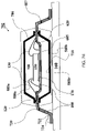
- FIG. 7A shows an example IC package 700 , according to an embodiment of the invention.
- a first cap 706 and a second cap 710 are coupled to leadframe 600 .
- First and second caps 706 and 710 may be configured in any manner as described for cap 510 above, and in other manners.
- a die 150 is mounted on the same side of DAP 605 as first cap 706 .
- First cap 706 is mounted to a top surface of leadframe 600 , such that die 150 resides in or below cavity 570 of first cap 706 .
- Second cap 710 is mounted to a bottom surface of leadframe 600 in an opposing configuration with respect to first cap 706 .
- Leadframe 600 and first cap 706 and 710 form an enclosure structure 702 that substantially encloses die 150 , providing improved structural integrity, EMI shielding, thermal performance, and environmental (e.g., mechanical shock, vibration, caustic, moisture, and radiation) protection.
- a cavity 708 is formed within enclosure structure 702 . Note that in embodiments, additional dies and/or other electrical components can be attached to DAP 605 .
- first and second caps 706 and 710 and leadframe 600 are made of copper or copper alloys.
- the thermal conductivity of copper is much greater than for typical encapsulating materials 120 (0.2-0.9 W/m ⁇ K). Therefore, the heat generated by die 150 is conducted through adhesive 170 to DAP 605 and out of the package through leads 607 and first and second caps 706 and 710 .
- first and second caps 706 and 710 and leadframe 600 are electrically connected in the embodiment of FIG.7A , they may form a near-equipotential surface, such that enclosure structure 702 approximates an ideal Faraday Cage. In this manner, die 150 is isolated from external EMI.
- copper and copper alloys have a much higher modulus of elasticity (about 125 GPa) compared to a typical cured plastic molding compound used for encapsulating material 120 (about 25 GPa), copper embodiments of the present invention provide improved structural rigidity and environmental protection.
- first and second caps 706 and 710 are coupled to leadframe 600 without the use of tabs and receptacles.
- first and second caps 706 and 710 have tabs 515 which fit corresponding receptacles 615 .
- Tabs 515 and corresponding receptacles 615 may facilitate tight lock-in of first and second caps 706 and 710 to leadframe 600 .
- the configuration of tabs 515 and receptacles 615 are such that first and second caps 706 and 710 will mate correctly with leadframe 600 in only one orientation, which may facilitate assembly.
- first and second caps 706 and 710 may have receptacles that interlock with tabs of leadframe 600 .
- Thermally and/or electrically conductive adhesive materials may be used to improve the coupling between first and second caps 706 and 710 and leadframe 600 .
- An adhesive material can be used to attach a tab 515 and a receptacle 615 , when they are present. Alternatively, the adhesive material may be used at areas where first and second caps 706 and 710 contact leadframe 600 .
- Leadframe 600 may be plated with a conductive material to improve thermal and electrical connection with first and/or second caps 706 and 710 .
- first and second caps 706 and 710 may be mounted to DAP 605 of leadframe 600 .
- first and second caps 706 and 710 are mounted to the tie-bars 620 coupled between DAP 605 and leads 607 .
- first and second caps 706 and 710 may be mounted to one or more leads 607 .
- first and second caps 706 and 710 can be mounted to any combination of DAP 605 , tie bars 620 , and leads 607 .
- first and second caps 706 and 710 may be coated with a layer of dielectric material (e.g. solder mask, dielectric film etc.) to prevent electrical shorting with one or more of leads 607 .
- first cap 706 and second cap 710 may be differently sized, and thus may be mounted to leadframe 600 differently. For example first cap 706 may be mounted to DAP 605 while second cap 710 is mounted to tie bars 620 .
- leads 607 of leadframe 600 are shaped to be coupled to a circuit board, where the circuit board could be a PCB, PWB, etc. as understood by someone skilled in the art.
- the circuit board could be a PCB, PWB, etc. as understood by someone skilled in the art.
- leads 607 may be bent to allow leads 607 to contact a PCB.
- leads 607 may be bent to form an “L” or “hockey stick” type shape, having a first bend 720 , and a second bend 722 .
- End portion 724 of leads 607 can be coupled to circuit board 160 , as shown in FIG. 7A .
- FIG. 7A As shown in FIG.
- leads 607 may be bent toward a side of package 700 away from die 150 to form a “die up” package.
- leads 607 may be bent toward a side of the package toward die 150 to form a “die down” package, (such as shown in FIGS. 7G and 7H ).
- Integrating an encapsulating material, such as glob top or plastic molding compound, with an enclosure structure, such as enclosure structure 702 may enhance the structural rigidity and planarity of the IC package.
- the combination of the encapsulating material and the enclosure structure may reduce IC die cracking and delamination.
- Integrating the encapsulating material with the enclosure structure also enhances environmental protection.
- the integrated package can provide protection against mechanical stress, impact, vibration, chemical corrosives, moistures, heat exposure, radiation, etc.
- attaching the IC die directly to the enclosure structure adds mass to the die support, and helps reduce microphonics.
- the metal traces of the IC die have electrical resistance, capacitance, and inductance.
- the IC die is under mechanical stress. Vibration, mechanical shock, or sudden change of temperature can cause a change of stress distribution within the IC die, and thus alter a capacitance and resistance such that a voltage vibration or drift is produced. This phenomenon is called microphonics. Attachment of the semiconductor die directly to the enclosure structure increases the mass and helps dampen these mechanical shocks and vibrations, thus reducing microphonics.
- Typical encapsulating materials such as plastic molding compound, have low thermal conductivity (e.g., about 0.2 to 0.9 W/m ⁇ K) and therefore create a bottleneck for heat dissipation in conventional IC packages.
- the enclosure structure eliminates this bottleneck by providing a thermally conductive path from the bottom surface of the IC die to the outer surfaces of the package.
- the enclosure structure is made with materials that have high thermal conductivity (e.g., approximately 390 W/m ⁇ K for copper) and therefore promote heat dissipation.
- Enclosure structure 702 formed by first and second caps 706 and 710 and leadframe 600 may be incorporated into IC packages of many different configurations.
- FIGS. 7A-7I illustrate some example embodiments of the present invention.
- package 700 of FIG. 7A shows die 150 attached to a DAP 605 with a thermally and/or electrically conductive adhesive 170 (such as an epoxy with metal or other conductive particles or flakes, solder, etc.).
- first and second caps 706 and 710 are coupled with leadframe 600 to form an enclosure structure 702 substantially enclosing die 150 .
- Package 700 is encapsulated in encapsulating material 120 (which may be formed in a mold).
- Package 700 may be mounted to a circuit board 160 , including printed wiring boards (PWBs).
- PWBs printed wiring boards
- at least one wirebond 130 couples at least one bond pad (not shown) on a surface of IC die 150 to leadframe 600 .
- a package may include first and second caps 706 and 710 having one or more openings (e.g. slots 520 and/or holes 530 ) as described elsewhere herein. These openings may act as mold gate openings, allowing encapsulating material 120 to flow or be injected into cavity 708 .
- first cap 706 has a surface 704 a and second cap 710 has surface 704 b that is exposed through the molding material 120 encapsulating package 700 .
- encapsulating material 120 does not cover caps 706 and 710 entirely.
- FIG. 7A second surface 585 a of cap 706 and second surface 585 b of second cap 710 is covered by encapsulating material 120 .
- FIG. 7B illustrates an embodiment where both first surface 580 a and second surface 585 a of first cap 706 and first and second surfaces 580 a and 585 b of second cap 710 are covered by encapsulating material 120 .
- FIG. 7C illustrates an embodiment where first and second caps 706 and 710 are not covered by encapsulating material 120 .
- An IC package may be in the form of this embodiment if first and second caps 706 and 710 are added to package 704 after encapsulating material 120 (e.g., a molding compound) has been applied.
- encapsulating material 120 e.g., a molding compound
- leadframe 600 may have tie bars 620 on a different plane than the leadframe bond fingers or leads 750 .
- tie bars 620 are above leads 750 .
- tie bars 620 are below leads 750 .
- the embodiment of FIG. 7E has the advantage of requiring shorter wirebonds 130 from the top of IC die 150 to leads 750 , relative to the embodiment of FIG. 7D .
- FIG. 7F shows an IC package 710 where first cap 706 is configured to mount an external heat sink 730 .
- Leadframe 600 and first cap 706 provide a path for heat to be conducted from die 150 to heat sink 730 , and thus out of package 710 .
- FIG. 7G illustrates a package 712 in a die-down configuration, according to an example embodiment of the present invention.
- surface 580 b of cap 710 is exposed on the bottom side of package 712 .
- the features reflected in the embodiments illustrated in FIGS. 7A-7F are applicable to the die-down configuration embodiments illustrated in FIGS. 7G and 7H .
- FIG. 7H illustrates a package 714 , according to another embodiment of the present invention. In package 714 , exposed surface 580 b of cap 710 is coupled to circuit board 160 with electrically and/or thermally conductive adhesive or solder 740 .
- the circuit board may be any type of circuit board such as a PCB, PWB, etc. as understood by someone skilled in the art.
- heat conducted from IC die 150 through leadframe 600 and cap 710 may be conducted out of package 714 into circuit board 160 .
- Surface 580 b of cap 710 may be electrically connected to a power pad or pads (not shown in FIG. 7H ) on circuit board 160 to improve EMI shielding and power delivery from package 714 .
- surface 580 b of cap 710 may be electrically connected to ground pad or pads (not shown in FIG. 7H ) on circuit board 160 to improve EMI shielding and current return from package 714 .
- Microphonics can further be reduced by using a leadframe IC package 704 structure as shown in FIG. 7I .
- FIG. 7I shows semiconductor die 150 not being encapsulated in a molding compound for environment protection.
- First and second caps 706 and 710 are attached to the leadframe 600 on both sides for environment protection and EMI shielding of semiconductor die 150 .
- An advantage of the embodiment of FIG. 7I is that mechanical stresses originated or transferred from the mold compound encapsulation on the IC die 150 are eliminated. This is desirable for reduction of microphonics in large scale integrated (LSI) electronic circuitry.
- LSI large scale integrated
- CTE coefficient of thermal expansion
- FIG. 7J shows IC package 718 where first and second caps 706 and 710 are completely encapsulated in the mold compound. Furthermore, caps 706 and 710 have slot openings 520 that can be used for mold flow during injection molding for die encapsulation.
- the metal cap cavity 708 diameter is large, mold flow through the openings on the sidewall of the metal cap into the center region above the die can be difficult and may require extremely high pressure for molding. It is often preferable then to have a plurality of circular openings on the top of the metal cap as shown in FIG. 5E for mold injection flow.
- FIG. 7K shows IC package 720 that is substantially similar to package 718 of FIG. 7J , however the surfaces of caps 706 and 710 are partially exposed on the top and bottom surfaces of the mold.
- FIG. 7L shows IC package 722 that is substantially similar to package 720 of FIG. 7K , however the surfaces of caps 706 and 710 are completely exposed on the top and bottom surfaces of the mold.
- FIG. 7M shows IC package 724 that is substantially similar to package 716 of FIG. 7I , but package 724 includes seal ring 716 that is used to seal gaps between the heat spreader tabs 750 and the lead frame 720 .
- the seal ring consists of an electrically non-conductive adhesive such as an epoxy, a thermoset adhesive, a molding compound, etc.
- FIGS. 11A-11C show different configurations for seal layer 716 .
- FIG. 11A shows a plan view of IC package 1100 where the seal ring 716 is shown to have separate sections. Although FIG. 11A shows seal ring 716 with two separate, in other embodiments the seal ring could have any number of sections as understood by someone skilled in the art.
- FIG. 11A shows seal ring 716 with two separate, in other embodiments the seal ring could have any number of sections as understood by someone skilled in the art.
- FIG. 11A shows seal ring 716 with two separate, in other embodiments the seal ring could have any number of sections as understood by someone
- FIG. 11B shows a plan view of IC package 1102 where the seal ring 716 is one continuous ring which is not closed. In preferred embodiments gaps where a ring is either not closed or gaps that separate sections are filled with air to allow pressure balance between the air within the cavity 708 (not shown) and the ambient.
- FIG. 11C shows a plan view of IC package 1104 where the seal ring 716 is one continuous ring which is not closed.
- first and second caps 706 and 710 maybe symmetrically placed on both sides (top and bottom) of leadframe 600 to form a symmetric cavity 708 (within enclosure structure 702 ). Thermal stress is compensated and reduced for in such symmetrically constructed packages.
- enclosure structure 702 may be filled with an inert gas like Helium, Neon, Argon, etc.
- first and second caps 706 and 710 add mass to the die support (e.g. DAP 605 ) that aid in reducing microphonics caused by stresses induced by vibration or shock. Attachment of semiconductor die 150 to the DAP 605 , which is suspended within enclosure structure 702 increases mass and helps damp mechanical shock or vibrations from affecting die 150 and package 704 .
- the die support e.g. DAP 605
- Attachment of semiconductor die 150 to the DAP 605 which is suspended within enclosure structure 702 increases mass and helps damp mechanical shock or vibrations from affecting die 150 and package 704 .
- FIG. 10A shows flowchart 1000 illustrating example steps to assemble leadframe package 700 shown in FIG. 7A , according to an embodiment of the present invention.
- FIG. 10B shows flowchart 1050 illustrating example steps for an alternate method to assemble package 700 .
- these assembly processes can be adapted to assemble any embodiments, including those illustrated in FIGS. 7A-7I .
- the steps in FIGS. 10A and 10B do not necessarily have to occur in the order shown, as will be apparent to persons skilled in the relevant art(s) based on the teachings herein. Other operational and structural embodiments will be apparent to persons skilled in the relevant art(s) based on the following discussion. These steps are described in detail below with respect to FIGS. 8A-8E and 9 A- 9 D, for illustrative purposes.
- FIGS. 8A-8E illustrate top views and FIGS. 9A-9D show side views of embodiments of the invention at different stages of assembly.
- Flowchart 1000 is shown in FIG. 10A , and begins with step 1005 .
- a leadframe 600 is formed from a sheet of material.
- Example leadframe materials and features are discussed elsewhere herein.
- FIG. 8A illustrates a view of a single leadframe 600 .
- FIG. 8B illustrates an example leadframe panel 800 that contains an array of leadframes 600 .
- Leadframes 600 in leadframe panel 800 may be manufactured by any of a variety of processes, including a molding process, an etching process or a stamping process, for example.
- step 1010 at least one IC die 150 is attached to a DAP 605 of a leadframe 600 .
- IC die 150 is attached using a thermally and/or electrically conductive adhesive 170 (such as solder or epoxy containing metal or other conductive particles or flakes).
- FIG. 9A illustrates a side view of an embodiment at this stage of assembly. For example, as shown in FIG. 9A a die 150 has been attached to each of DAPs 605 a - e.
- wirebonds 130 are interconnected between pads of IC die 150 and leadframe 600 , providing electrical connections from IC die 150 to leads 607 , tie bars 620 , and/or DAP 605 .
- first cap 706 is attached to leadframe 600 .
- FIG. 8C shows a partially assembled package 810 , illustrating an example embodiment leadframe package at this stage of assembly. As shown in FIG. 8C , first cap 706 is mounted to leadframe 600 .
- FIG. 8E illustrates a partially assembled panel 820 of partially assembled packages 810 .
- FIG. 9B shows a side view of partially assembled panel 820 . As shown in FIG. 9B , a first cap 706 is coupled to each of leadframes 600 a - 600 e.
- second cap 710 is attached to leadframe 600 .
- second cap 710 is mounted to leadframe 600 .
- Electrically and/or thermally conductive adhesive materials may be used to improve coupling between first cap 706 , second cap 710 and leadframe 600 .
- First cap 706 , second cap 710 and leadframe 600 are joined to form an enclosure structure (e.g., enclosure structure 702 ) which substantially encloses IC die 150 .
- a second cap 710 is coupled to each of leadframes 600 a - 600 e.
- an encapsulating process encapsulates partially assembled package 810 in encapsulating material 120 .
- package or packages 810 may be clamped in a mold chassis to mold or shape a molding compound being used to encapsulate the package.
- FIG. 9D shows a side view of an encapsulated panel 910 of leadframe packages 700 at this stage of assembly.
- an outer peripheral dimension of first and second caps 706 and 710 is smaller than a peripheral dimension of peripheral support ring 630 . This prevents the encapsulating material from bleeding through gaps between leads 607 .
- Inner support ring 630 may also provide sealing between the clamped mold chassis during the transfer molding process.
- Leads 607 are ready to be formed into contact pins for board mount and a leadframe package 700 is completely assembled.
- the outer portion of leads 607 extending from the package may be bent to allow them to contact a circuit board, where the circuit board could be a PCB, PWB, etc. as understood by someone skilled in the art.
- leads 607 may be bent to form an “L” or “hockey stick” type shape.
- leads 607 may be bent toward a side of the package away from die 150 to form a “die up” package, or may be bent toward a side of the package toward die 150 to form a “die down” package.
- Steps 1005 - 1015 are the same as shown in FIG. 10A .
- leadframe 600 and first and second caps 706 and 710 are put into the mold chassis for steps 1055 , 1060 and 1062 .
- step 1065 a molding process takes place.
- leadframe 600 , first cap 510 and second cap 710 are coupled together, and in an embodiment, may be held together by a molding compound.
- FIGS. 12A-12B illustrate an example design for a cap.
- FIG. 12A shows a horizontal view and
- FIG. 12B shows a top view of cap 1200 shaped as an inverted cup with slot openings 520 and standoff distance 1202 which has leadframe contact stands on it four corners.
- FIGS. 13A-13B show horizontal and top views respectively of another example design cap substantially similar to cap 1200 shown in FIGS. 12A-12B .
- cap 1300 also has leadframe contact stands with fused leads 1302 .
- the location of the contact stands 1302 can be optimized based on leadframe design.
Abstract
Description
Claims (30)
Priority Applications (5)
| Application Number | Priority Date | Filing Date | Title |
|---|---|---|---|
| US11/527,573 US7808087B2 (en) | 2006-06-01 | 2006-09-27 | Leadframe IC packages having top and bottom integrated heat spreaders |
| EP07004088A EP1863086A3 (en) | 2006-06-01 | 2007-02-27 | Leadframe IC packages having top and bottom integrated heat spreaders |
| KR1020070051891A KR100931900B1 (en) | 2006-06-01 | 2007-05-29 | Leadframe IC package with integrated heat spreaders at the top and bottom |
| TW096119312A TW200818422A (en) | 2006-06-01 | 2007-05-30 | Leadframe IC packages having top and bottom integrated heat spreaders |
| HK08104909.4A HK1115228A1 (en) | 2006-06-01 | 2008-05-02 | Leadframe ic packages having top and bottom integrated heat spreaders |
Applications Claiming Priority (2)
| Application Number | Priority Date | Filing Date | Title |
|---|---|---|---|
| US80368106P | 2006-06-01 | 2006-06-01 | |
| US11/527,573 US7808087B2 (en) | 2006-06-01 | 2006-09-27 | Leadframe IC packages having top and bottom integrated heat spreaders |
Publications (2)
| Publication Number | Publication Date |
|---|---|
| US20070278632A1 US20070278632A1 (en) | 2007-12-06 |
| US7808087B2 true US7808087B2 (en) | 2010-10-05 |
Family
ID=38508836
Family Applications (1)
| Application Number | Title | Priority Date | Filing Date |
|---|---|---|---|
| US11/527,573 Active 2027-11-25 US7808087B2 (en) | 2006-06-01 | 2006-09-27 | Leadframe IC packages having top and bottom integrated heat spreaders |
Country Status (5)
| Country | Link |
|---|---|
| US (1) | US7808087B2 (en) |
| EP (1) | EP1863086A3 (en) |
| KR (1) | KR100931900B1 (en) |
| HK (1) | HK1115228A1 (en) |
| TW (1) | TW200818422A (en) |
Cited By (41)
| Publication number | Priority date | Publication date | Assignee | Title |
|---|---|---|---|---|
| US20090284932A1 (en) * | 2008-03-25 | 2009-11-19 | Bridge Semiconductor Corporation | Thermally Enhanced Package with Embedded Metal Slug and Patterned Circuitry |
| US20100003787A1 (en) * | 2008-03-25 | 2010-01-07 | Bridge Semiconductor Corporation | Method of making a semiconductor chip assembly with a post/base heat spreader and horizontal signal routing |
| US20100052005A1 (en) * | 2008-03-25 | 2010-03-04 | Lin Charles W C | Semiconductor chip assembly with post/base heat spreader and conductive trace |
| US20100072511A1 (en) * | 2008-03-25 | 2010-03-25 | Lin Charles W C | Semiconductor chip assembly with copper/aluminum post/base heat spreader |
| US20100075448A1 (en) * | 2008-03-25 | 2010-03-25 | Bridge Semiconductor Corporation | Method of making a semiconductor chip assembly with a post/base/cap heat spreader |
| US20100096662A1 (en) * | 2008-03-25 | 2010-04-22 | Bridge Semiconductor Corporation | Semiconductor chip assembly with post/base heat spreader and signal post |
| US20100155768A1 (en) * | 2008-03-25 | 2010-06-24 | Bridge Semiconductor Corporation | Semiconductor chip assembly with post/base heat spreader and cavity in post |
| US20100155769A1 (en) * | 2008-03-25 | 2010-06-24 | Bridge Semiconductor Corporation | Semiconductor chip assembly with base heat spreader and cavity in base |
| US20100163921A1 (en) * | 2008-03-25 | 2010-07-01 | Bridge Semiconductor Corporation | Semiconductor chip assembly with aluminum post/base heat spreader and silver/copper conductive trace |
| US20100181594A1 (en) * | 2008-03-25 | 2010-07-22 | Lin Charles W C | Semiconductor chip assembly with post/base heat spreader and cavity over post |
| US20100193830A1 (en) * | 2008-03-25 | 2010-08-05 | Bridge Semiconductor Corporation | Semiconductor chip assembly with post/base heat spreader and dual adhesives |
| US20100289054A1 (en) * | 2008-03-25 | 2010-11-18 | Bridge Semiconductor Corporation | Semiconductor chip assembly with post/base heat spreader and adhesive between base and terminal |
| US20100327310A1 (en) * | 2008-03-25 | 2010-12-30 | Lin Charles W C | Semiconductor chip assembly with post/base/flange heat spreader and cavity in flange |
| US20110039374A1 (en) * | 2008-03-25 | 2011-02-17 | Bridge Semiconductor Corporation | Method of making a semiconductor chip assembly with a bump/base heat spreader and a cavity in the bump |
| US20110065241A1 (en) * | 2008-03-25 | 2011-03-17 | Bridge Semiconductor Corporation | Method of making a semiconductor chip assembly with a bump/base heat spreader and a dual-angle cavity in the bump |
| US20110101410A1 (en) * | 2008-03-25 | 2011-05-05 | Lin Charles W C | Semiconductor chip assembly with post/base/post heat spreader |
| US20110127653A1 (en) * | 2009-12-02 | 2011-06-02 | Reza Argenty Pagaila | Package system with a shielded inverted internal stacking module and method of manufacture thereof |
| US20110151626A1 (en) * | 2008-03-25 | 2011-06-23 | Lin Charles W C | Method of making a semiconductor chip assembly with a post/base/post heat spreader and asymmetric posts |
| US20110163348A1 (en) * | 2008-03-25 | 2011-07-07 | Bridge Semiconductor Corporation | Semiconductor chip assembly with bump/base heat spreader and inverted cavity in bump |
| US20110201157A1 (en) * | 2008-03-25 | 2011-08-18 | Bridge Semiconductor Corporation. | Method of making a semiconductor chip assembly with a post/base heat spreader and a multilevel conductive trace |
| US8003415B2 (en) | 2008-03-25 | 2011-08-23 | Bridge Semiconductor Corporation | Method of making a semiconductor chip assembly with a post/base heat spreader and vertical signal routing |
| US20110228507A1 (en) * | 2010-03-16 | 2011-09-22 | Intersil Americas Inc. | Molded power-supply module with bridge inductor over other components |
| US8097934B1 (en) * | 2007-09-27 | 2012-01-17 | National Semiconductor Corporation | Delamination resistant device package having low moisture sensitivity |
| US8110446B2 (en) | 2008-03-25 | 2012-02-07 | Bridge Semiconductor Corporation | Method of making a semiconductor chip assembly with a post/base heat spreader and a conductive trace |
| US8129742B2 (en) | 2008-03-25 | 2012-03-06 | Bridge Semiconductor Corporation | Semiconductor chip assembly with post/base heat spreader and plated through-hole |
| US20120063038A1 (en) * | 2010-09-10 | 2012-03-15 | Intersil Americas Inc. | Power-supply module with electromagnetic-interference (emi) shielding, cooling, or both shielding and cooling, along two or more sides |
| US8153477B2 (en) | 2008-03-25 | 2012-04-10 | Bridge Semiconductor Corporation | Method of making a semiconductor chip assembly with a post/dielectric/post heat spreader |
| US8178395B2 (en) | 2008-03-25 | 2012-05-15 | Bridge Semiconductor Corporation | Method of making a semiconductor chip assembly with a post/base heat spreader with a thermal via |
| US8212279B2 (en) | 2008-03-25 | 2012-07-03 | Bridge Semiconductor Corporation | Semiconductor chip assembly with post/base heat spreader, signal post and cavity |
| US8232576B1 (en) | 2008-03-25 | 2012-07-31 | Bridge Semiconductor Corporation | Semiconductor chip assembly with post/base heat spreader and ceramic block in post |
| US8304292B1 (en) | 2009-08-06 | 2012-11-06 | Bridge Semiconductor Corporation | Method of making a semiconductor chip assembly with a ceramic/metal substrate |
| US8310043B2 (en) | 2008-03-25 | 2012-11-13 | Bridge Semiconductor Corporation | Semiconductor chip assembly with post/base heat spreader with ESD protection layer |
| US8329510B2 (en) | 2008-03-25 | 2012-12-11 | Bridge Semiconductor Corporation | Method of making a semiconductor chip assembly with a post/base heat spreader with an ESD protection layer |
| US8354688B2 (en) | 2008-03-25 | 2013-01-15 | Bridge Semiconductor Corporation | Semiconductor chip assembly with bump/base/ledge heat spreader, dual adhesives and cavity in bump |
| US8637963B2 (en) | 2011-10-05 | 2014-01-28 | Sandisk Technologies Inc. | Radiation-shielded semiconductor device |
| US8853834B2 (en) | 2012-12-13 | 2014-10-07 | Powertech Technology Inc. | Leadframe-type semiconductor package having EMI shielding layer connected to ground |
| US9349940B2 (en) * | 2014-09-17 | 2016-05-24 | Kabushiki Kaisha Toshiba | Semiconductor device and method of manufacturing the same |
| US9466545B1 (en) * | 2007-02-21 | 2016-10-11 | Amkor Technology, Inc. | Semiconductor package in package |
| US20180220539A1 (en) * | 2015-09-29 | 2018-08-02 | Hitachi Automotive Systems, Ltd. | Electronic Control Device |
| US20220028798A1 (en) * | 2020-07-21 | 2022-01-27 | UTAC Headquarters Pte. Ltd. | Semiconductor packages with integrated shielding |
| US11616027B2 (en) | 2019-12-17 | 2023-03-28 | Analog Devices International Unlimited Company | Integrated circuit packages to minimize stress on a semiconductor die |
Families Citing this family (72)
| Publication number | Priority date | Publication date | Assignee | Title |
|---|---|---|---|---|
| US7271479B2 (en) * | 2004-11-03 | 2007-09-18 | Broadcom Corporation | Flip chip package including a non-planar heat spreader and method of making the same |
| US7582951B2 (en) | 2005-10-20 | 2009-09-01 | Broadcom Corporation | Methods and apparatus for improved thermal performance and electromagnetic interference (EMI) shielding in leadframe integrated circuit (IC) packages |
| US20070200210A1 (en) * | 2006-02-28 | 2007-08-30 | Broadcom Corporation | Methods and apparatus for improved thermal performance and electromagnetic interference (EMI) shielding in integrated circuit (IC) packages |
| US7714453B2 (en) | 2006-05-12 | 2010-05-11 | Broadcom Corporation | Interconnect structure and formation for package stacking of molded plastic area array package |
| US9299634B2 (en) * | 2006-05-16 | 2016-03-29 | Broadcom Corporation | Method and apparatus for cooling semiconductor device hot blocks and large scale integrated circuit (IC) using integrated interposer for IC packages |
| US8183680B2 (en) | 2006-05-16 | 2012-05-22 | Broadcom Corporation | No-lead IC packages having integrated heat spreader for electromagnetic interference (EMI) shielding and thermal enhancement |
| US20070273023A1 (en) * | 2006-05-26 | 2007-11-29 | Broadcom Corporation | Integrated circuit package having exposed thermally conducting body |
| US7808087B2 (en) | 2006-06-01 | 2010-10-05 | Broadcom Corporation | Leadframe IC packages having top and bottom integrated heat spreaders |
| US8581381B2 (en) | 2006-06-20 | 2013-11-12 | Broadcom Corporation | Integrated circuit (IC) package stacking and IC packages formed by same |
| US9013035B2 (en) * | 2006-06-20 | 2015-04-21 | Broadcom Corporation | Thermal improvement for hotspots on dies in integrated circuit packages |
| US8183687B2 (en) | 2007-02-16 | 2012-05-22 | Broadcom Corporation | Interposer for die stacking in semiconductor packages and the method of making the same |
| US7872335B2 (en) * | 2007-06-08 | 2011-01-18 | Broadcom Corporation | Lead frame-BGA package with enhanced thermal performance and I/O counts |
| US20090014856A1 (en) * | 2007-07-10 | 2009-01-15 | International Business Machine Corporation | Microbump seal |
| US7902644B2 (en) * | 2007-12-07 | 2011-03-08 | Stats Chippac Ltd. | Integrated circuit package system for electromagnetic isolation |
| US7832278B2 (en) * | 2008-05-29 | 2010-11-16 | Hong Kong Applied Science And Technology Research Institute Co., Ltd. | Multi-chip package |
| US9219956B2 (en) | 2008-12-23 | 2015-12-22 | Keyssa, Inc. | Contactless audio adapter, and methods |
| US8554136B2 (en) | 2008-12-23 | 2013-10-08 | Waveconnex, Inc. | Tightly-coupled near-field communication-link connector-replacement chips |
| US9954579B2 (en) | 2008-12-23 | 2018-04-24 | Keyssa, Inc. | Smart connectors and associated communications links |
| US9474099B2 (en) | 2008-12-23 | 2016-10-18 | Keyssa, Inc. | Smart connectors and associated communications links |
| US9191263B2 (en) | 2008-12-23 | 2015-11-17 | Keyssa, Inc. | Contactless replacement for cabled standards-based interfaces |
| US9960820B2 (en) | 2008-12-23 | 2018-05-01 | Keyssa, Inc. | Contactless data transfer systems and methods |
| TWI392065B (en) * | 2009-06-08 | 2013-04-01 | Cyntec Co Ltd | Electronic element packaging module |
| US8531012B2 (en) * | 2009-10-23 | 2013-09-10 | Stats Chippac, Ltd. | Semiconductor device and method of forming a shielding layer over a semiconductor die disposed in a cavity of an interconnect structure and grounded through the die TSV |
| US20120126378A1 (en) * | 2010-11-24 | 2012-05-24 | Unisem (Mauritius ) Holdings Limited | Semiconductor device package with electromagnetic shielding |
| CN102683222A (en) | 2011-03-18 | 2012-09-19 | 飞思卡尔半导体公司 | Method for packaging semiconductor pipe cores with cover cap components |
| JP2014510493A (en) | 2011-03-24 | 2014-04-24 | ウェーブコネックス・インコーポレーテッド | Integrated circuit for electromagnetic communication |
| CN102738022B (en) | 2011-04-15 | 2017-05-17 | 飞思卡尔半导体公司 | Method for assembling semiconductor device containing insulating substrate and heat sink |
| US9614590B2 (en) | 2011-05-12 | 2017-04-04 | Keyssa, Inc. | Scalable high-bandwidth connectivity |
| US8714459B2 (en) | 2011-05-12 | 2014-05-06 | Waveconnex, Inc. | Scalable high-bandwidth connectivity |
| US8811526B2 (en) | 2011-05-31 | 2014-08-19 | Keyssa, Inc. | Delta modulated low power EHF communication link |
| WO2012174350A1 (en) | 2011-06-15 | 2012-12-20 | Waveconnex, Inc. | Proximity sensing and distance measurement using ehf signals |
| FR2977975A1 (en) * | 2011-07-13 | 2013-01-18 | St Microelectronics Grenoble 2 | THERMAL VIA ELECTRONIC HOUSING AND METHOD OF MANUFACTURE |
| CN102956509A (en) | 2011-08-31 | 2013-03-06 | 飞思卡尔半导体公司 | Power device and method for packaging same |
| JP5844472B2 (en) | 2011-09-15 | 2016-01-20 | ケッサ・インコーポレーテッド | Wireless communication using dielectric media |
| CN104115417A (en) | 2011-10-20 | 2014-10-22 | 基萨公司 | Low-profile wireless connectors |
| TWI633766B (en) | 2011-10-21 | 2018-08-21 | 奇沙公司 | Devices and sysytems for contactless signal splicing |
| EP2792031A1 (en) | 2011-12-14 | 2014-10-22 | Keyssa, Inc. | Connectors providing haptic feedback |
| US9559790B2 (en) | 2012-01-30 | 2017-01-31 | Keyssa, Inc. | Link emission control |
| US9344201B2 (en) | 2012-01-30 | 2016-05-17 | Keyssa, Inc. | Shielded EHF connector assemblies |
| KR101578472B1 (en) | 2012-03-02 | 2015-12-17 | 키사, 아이엔씨. | Systems and methods for duplex communication |
| CN106921445A (en) | 2012-03-06 | 2017-07-04 | 凯萨股份有限公司 | System for constraining the operating parameter of EHF communication chips |
| US9553353B2 (en) | 2012-03-28 | 2017-01-24 | Keyssa, Inc. | Redirection of electromagnetic signals using substrate structures |
| WO2013158786A1 (en) | 2012-04-17 | 2013-10-24 | Waveconnex, Inc. | Dielectric lens structures for interchip communication |
| JP2013243263A (en) * | 2012-05-21 | 2013-12-05 | Internatl Business Mach Corp <Ibm> | Combination of power supply and heat dissipation (cooling) in three-dimensional laminate package |
| KR20150041653A (en) | 2012-08-10 | 2015-04-16 | 키사, 아이엔씨. | Dielectric coupling systems for ehf communications |
| JP5813596B2 (en) * | 2012-08-10 | 2015-11-17 | 株式会社東芝 | Nonvolatile semiconductor memory device |
| WO2014043577A1 (en) | 2012-09-14 | 2014-03-20 | Waveconnex, Inc. | Wireless connections with virtual hysteresis |
| EP2932556B1 (en) | 2012-12-17 | 2017-06-07 | Keyssa, Inc. | Modular electronics |
| US20140210062A1 (en) * | 2013-01-28 | 2014-07-31 | Texas Instruments Incorporated | Leadframe-Based Semiconductor Package Having Terminals on Top and Bottom Surfaces |
| KR101700789B1 (en) | 2013-03-15 | 2017-01-31 | 키사, 아이엔씨. | Extremely high frequency communication chip |
| WO2014149107A1 (en) | 2013-03-15 | 2014-09-25 | Waveconnex, Inc. | Ehf secure communication device |
| JP5802695B2 (en) * | 2013-03-19 | 2015-10-28 | 株式会社東芝 | Semiconductor device and method for manufacturing semiconductor device |
| ITVI20130077A1 (en) | 2013-03-20 | 2014-09-21 | St Microelectronics Srl | A GRAPHENE-BASED FILLER MATERIAL WITH A HIGH THERMAL CONDUCTIVITY FOR THE CONNECTION OF CHIPS IN MICRO-STRUCTURE DEVICES |
| KR101459566B1 (en) * | 2013-06-19 | 2014-11-10 | 시그네틱스 주식회사 | Heatslug, semiconductor package comprising the same heatslug, and method for fabricating the same semiconductor package |
| US9064838B2 (en) * | 2013-09-17 | 2015-06-23 | Freescale Semiconductor, Inc. | Heat spreader for integrated circuit device |
| US10032726B1 (en) * | 2013-11-01 | 2018-07-24 | Amkor Technology, Inc. | Embedded vibration management system |
| US9602648B2 (en) | 2015-04-30 | 2017-03-21 | Keyssa Systems, Inc. | Adapter devices for enhancing the functionality of other devices |
| JP6437406B2 (en) * | 2015-09-15 | 2018-12-12 | 東芝メモリ株式会社 | Semiconductor device manufacturing method, semiconductor device, and lead frame |
| US10049801B2 (en) | 2015-10-16 | 2018-08-14 | Keyssa Licensing, Inc. | Communication module alignment |
| US10043763B2 (en) * | 2015-12-19 | 2018-08-07 | Skyworks Solutions, Inc. | Shielded lead frame packages |
| US20170287838A1 (en) | 2016-04-02 | 2017-10-05 | Intel Corporation | Electrical interconnect bridge |
| IT201700000485A1 (en) * | 2017-01-03 | 2018-07-03 | St Microelectronics Srl | CORRESPONDING EQUIPMENT, SEMICONDUCTOR AND EQUIPMENT |
| US10714430B2 (en) * | 2017-07-21 | 2020-07-14 | Octavo Systems Llc | EMI shield for molded packages |
| KR102063469B1 (en) * | 2018-05-04 | 2020-01-09 | 삼성전자주식회사 | Fan-out semiconductor package |
| US10840164B2 (en) | 2018-05-18 | 2020-11-17 | Infineon Technologies Ag | Wire bonded package with single piece exposed heat slug and leads |
| DE112020000716T5 (en) * | 2019-02-08 | 2021-11-25 | Ams International Ag | REDUCING THE SENSITIVITY OF INTEGRATED CIRCUITS AND SENSORS TO HIGH FREQUENCY INTERFERENCE |
| US10914018B2 (en) * | 2019-03-12 | 2021-02-09 | Infineon Technologies Ag | Porous Cu on Cu surface for semiconductor packages |
| US10978380B2 (en) * | 2019-05-03 | 2021-04-13 | Infineon Technologies Ag | Semiconductor package with multi-level conductive clip for top side cooling |
| US11075185B2 (en) * | 2019-05-03 | 2021-07-27 | Infineon Technologies Ag | Semiconductor package with multi-level conductive clip for top side cooling |
| US11121094B2 (en) * | 2019-06-20 | 2021-09-14 | Amkor Technology Singapore Holding Pte. Ltd. | Semiconductor devices with shield |
| US11659663B2 (en) | 2020-10-07 | 2023-05-23 | Murata Manufacturing Co., Ltd. | Mechanical support within moulded chip package |
| CN116435201B (en) * | 2023-06-12 | 2023-09-12 | 四川遂宁市利普芯微电子有限公司 | Plastic packaging method and device packaging structure |
Citations (95)
| Publication number | Priority date | Publication date | Assignee | Title |
|---|---|---|---|---|
| GB1306031A (en) | 1971-01-01 | 1973-02-07 | ||
| US4480262A (en) | 1982-07-15 | 1984-10-30 | Olin Corporation | Semiconductor casing |
| US4560826A (en) | 1983-12-29 | 1985-12-24 | Amp Incorporated | Hermetically sealed chip carrier |
| US4680613A (en) | 1983-12-01 | 1987-07-14 | Fairchild Semiconductor Corporation | Low impedance package for integrated circuit die |
| US4803544A (en) | 1986-07-11 | 1989-02-07 | Junghans Uhren Gmbh | Prefabricated strip conductor network assembly unit and process for making same |
| US5105260A (en) | 1989-10-31 | 1992-04-14 | Sgs-Thomson Microelectronics, Inc. | Rf transistor package with nickel oxide barrier |
| US5153379A (en) | 1990-10-09 | 1992-10-06 | Motorola, Inc. | Shielded low-profile electronic component assembly |
| EP0573297A2 (en) | 1992-06-04 | 1993-12-08 | Shinko Electric Industries Co. Ltd. | Semiconductor device comprising a TAB tape |
| US5294826A (en) * | 1993-04-16 | 1994-03-15 | Northern Telecom Limited | Integrated circuit package and assembly thereof for thermal and EMI management |
| US5350943A (en) | 1992-04-18 | 1994-09-27 | Temic Telefunken Microelectronic Gmbh | Semiconductor assembly, in particular a remote control reception module |
| US5376756A (en) | 1991-12-20 | 1994-12-27 | Vlsi Technology, Inc. | Wire support and guide |
| US5378656A (en) * | 1992-03-27 | 1995-01-03 | Hitachi, Ltd. | Leadframe, semiconductor integrated circuit device using the same, and method of and process for fabricating the same |
| US5389816A (en) | 1992-11-19 | 1995-02-14 | Shinko Electric Industries Co., Ltd. | Multi-layer lead frame using a metal-core substrate |
| US5406117A (en) | 1993-12-09 | 1995-04-11 | Dlugokecki; Joseph J. | Radiation shielding for integrated circuit devices using reconstructed plastic packages |
| US5457341A (en) | 1994-05-03 | 1995-10-10 | Texas Instruments Incorporated | Integrated circuit device and manufacturing method using photoresist lead covering |
| US5468910A (en) | 1993-08-02 | 1995-11-21 | Motorola, Inc. | Semiconductor device package and method of making |
| US5486720A (en) | 1994-05-26 | 1996-01-23 | Analog Devices, Inc. | EMF shielding of an integrated circuit package |
| US5497032A (en) | 1993-03-17 | 1996-03-05 | Fujitsu Limited | Semiconductor device and lead frame therefore |
| US5559306A (en) * | 1994-05-17 | 1996-09-24 | Olin Corporation | Electronic package with improved electrical performance |
| US5608265A (en) | 1993-03-17 | 1997-03-04 | Hitachi, Ltd. | Encapsulated semiconductor device package having holes for electrically conductive material |
| US5614761A (en) * | 1991-02-28 | 1997-03-25 | Hitachi, Ltd. | Electronic circuit package including plural semiconductor chips formed on a wiring substrate |
| US5642261A (en) | 1993-12-20 | 1997-06-24 | Sgs-Thomson Microelectronics, Inc. | Ball-grid-array integrated circuit package with solder-connected thermal conductor |
| US5650659A (en) * | 1995-08-04 | 1997-07-22 | National Semiconductor Corporation | Semiconductor component package assembly including an integral RF/EMI shield |
| US5668406A (en) | 1994-05-31 | 1997-09-16 | Nec Corporation | Semiconductor device having shielding structure made of electrically conductive paste |
| DE19700056A1 (en) | 1996-03-22 | 1997-09-25 | Mitsubishi Electric Corp | Semiconductor module with mounting region for semiconductor element |
| US5691567A (en) | 1995-09-19 | 1997-11-25 | National Semiconductor Corporation | Structure for attaching a lead frame to a heat spreader/heat slug structure |
| US5703398A (en) * | 1993-03-17 | 1997-12-30 | Fujitsu Limited | Semiconductor integrated circuit device and method of producing the semiconductor integrated circuit device |
| US5723899A (en) * | 1994-08-30 | 1998-03-03 | Amkor Electronics, Inc. | Semiconductor lead frame having connection bar and guide rings |
| US5825042A (en) * | 1993-06-18 | 1998-10-20 | Space Electronics, Inc. | Radiation shielding of plastic integrated circuits |
| US5977626A (en) | 1998-08-12 | 1999-11-02 | Industrial Technology Research Institute | Thermally and electrically enhanced PBGA package |
| US5986340A (en) | 1996-05-02 | 1999-11-16 | National Semiconductor Corporation | Ball grid array package with enhanced thermal and electrical characteristics and electronic device incorporating same |
| US6011303A (en) | 1996-11-29 | 2000-01-04 | Nec Corporation | Electronic component |
| US6092281A (en) | 1998-08-28 | 2000-07-25 | Amkor Technology, Inc. | Electromagnetic interference shield driver and method |
| US6221702B1 (en) | 1998-02-10 | 2001-04-24 | Lg. Philips Lcd Co., Ltd. | Method of fabricating thin film transistor |
| US6229702B1 (en) | 1999-06-02 | 2001-05-08 | Advanced Semiconductor Engineering, Inc. | Ball grid array semiconductor package having improved heat dissipation efficiency, overall electrical performance and enhanced bonding capability |
| US20020024137A1 (en) | 2000-08-08 | 2002-02-28 | Lars-Anders Olofsson | Method of securing solder balls and any components fixed to one and the same side of a substrate |
| US6395582B1 (en) | 1997-07-14 | 2002-05-28 | Signetics | Methods for forming ground vias in semiconductor packages |
| US20020079572A1 (en) | 2000-12-22 | 2002-06-27 | Khan Reza-Ur Rahman | Enhanced die-up ball grid array and method for making the same |
| US20020098617A1 (en) | 2001-01-20 | 2002-07-25 | Ming-Xun Lee | CD BGA package and a fabrication method thereof |
| US6432742B1 (en) | 2000-08-17 | 2002-08-13 | St Assembly Test Services Pte Ltd. | Methods of forming drop-in heat spreader plastic ball grid array (PBGA) packages |
| US6501184B1 (en) | 1999-05-20 | 2002-12-31 | Amkor Technology, Inc. | Semiconductor package and method for manufacturing the same |
| US20030025089A1 (en) | 1994-04-01 | 2003-02-06 | Maxwell Electronic Components Group, Inc. | Methods and compositions for ionizing radiation shielding |
| US6528876B2 (en) | 2000-06-26 | 2003-03-04 | Siliconware Precision Industries Co., Ltd. | Semiconductor package having heat sink attached to substrate |
| US20030057550A1 (en) | 2000-12-22 | 2003-03-27 | Broadcom Corporation | Ball grid array package enhanced with a thermal and electrical connector |
| US6552428B1 (en) | 1998-10-12 | 2003-04-22 | Siliconware Precision Industries Co., Ltd. | Semiconductor package having an exposed heat spreader |
| US20030111728A1 (en) | 2001-09-26 | 2003-06-19 | Thai Cao Minh | Mounting material, semiconductor device and method of manufacturing semiconductor device |
| US20030146509A1 (en) | 2002-02-01 | 2003-08-07 | Broadcom Corporation | Ball grid array package with separated stiffener layer |
| US6614102B1 (en) * | 2001-05-04 | 2003-09-02 | Amkor Technology, Inc. | Shielded semiconductor leadframe package |
| US6617200B2 (en) | 2000-07-05 | 2003-09-09 | Seiko Epson Corporation | System and method for fabricating a semiconductor device |
| US20030178719A1 (en) | 2002-03-22 | 2003-09-25 | Combs Edward G. | Enhanced thermal dissipation integrated circuit package and method of manufacturing enhanced thermal dissipation integrated circuit package |
| US20040038447A1 (en) | 2002-08-21 | 2004-02-26 | Corisis David J | Packaged microelectronic devices and methods for assembling microelectronic devices |
| US6707140B1 (en) | 2000-05-09 | 2004-03-16 | National Semiconductor Corporation | Arrayable, scaleable, and stackable molded package configuration |
| US20040084771A1 (en) | 2002-11-05 | 2004-05-06 | Micron Technology, Inc. | Methods and apparatus for a thin stacked ball-grid array package |
| US6737750B1 (en) | 2001-12-07 | 2004-05-18 | Amkor Technology, Inc. | Structures for improving heat dissipation in stacked semiconductor packages |
| US6775140B2 (en) | 2002-10-21 | 2004-08-10 | St Assembly Test Services Ltd. | Heat spreaders, heat spreader packages, and fabrication methods for use with flip chip semiconductor devices |
| US20040178499A1 (en) | 2003-03-10 | 2004-09-16 | Mistry Addi B. | Semiconductor package with multiple sides having package contacts |
| US6825108B2 (en) | 2002-02-01 | 2004-11-30 | Broadcom Corporation | Ball grid array package fabrication with IC die support structures |
| US6838761B2 (en) | 2002-09-17 | 2005-01-04 | Chippac, Inc. | Semiconductor multi-package module having wire bond interconnect between stacked packages and having electrical shield |
| US20050012203A1 (en) | 2001-02-15 | 2005-01-20 | Rahman Khan Reza-Ur | Enhanced die-down ball grid array and method for making the same |
| US6848912B2 (en) | 2002-12-12 | 2005-02-01 | Broadcom Corporation | Via providing multiple electrically conductive paths through a circuit board |
| US20050035452A1 (en) | 2001-05-07 | 2005-02-17 | Broadcom Corporation | Die-up ball grid array package including a substrate having an opening and method for making the same |
| US6861750B2 (en) | 2002-02-01 | 2005-03-01 | Broadcom Corporation | Ball grid array package with multiple interposers |
| US6876553B2 (en) | 2002-03-21 | 2005-04-05 | Broadcom Corporation | Enhanced die-up ball grid array package with two substrates |
| US6879039B2 (en) | 2001-12-18 | 2005-04-12 | Broadcom Corporation | Ball grid array package substrates and method of making the same |
| US20050077545A1 (en) | 2000-12-01 | 2005-04-14 | Broadcom Corporation | Ball grid array package with patterned stiffener surface and method of assembling the same |
| US6906414B2 (en) | 2000-12-22 | 2005-06-14 | Broadcom Corporation | Ball grid array package with patterned stiffener layer |
| US6919630B2 (en) | 2003-03-27 | 2005-07-19 | Siliconware Precision Industries Co. Ltd. | Semiconductor package with heat spreader |
| US20050199987A1 (en) | 2002-04-30 | 2005-09-15 | Tadatoshi Danno | Semiconductor device and electronic device |
| US20050280139A1 (en) | 2004-06-21 | 2005-12-22 | Broadcom Corporation | Multipiece apparatus for thermal and electromagnetic interference (EMI) shielding enhancement in die-up array packages and method of making the same |
| US20050280127A1 (en) * | 2004-06-21 | 2005-12-22 | Broadcom Corporation | Apparatus and method for thermal and electromagnetic interference (EMI) shielding enhancement in die-up array packages |
| US20050280141A1 (en) | 2004-06-21 | 2005-12-22 | Broadcom Corporation | Integrated circuit device package having both wire bond and flip-chip interconnections and method of making the same |
| US20060012037A1 (en) | 2004-07-01 | 2006-01-19 | Raedt Walter D | Methods for bonding and devices according to such methods |
| US7015072B2 (en) | 2001-07-11 | 2006-03-21 | Asat Limited | Method of manufacturing an enhanced thermal dissipation integrated circuit package |
| US7015379B2 (en) | 2005-01-31 | 2006-03-21 | Pioneer Hi-Bred International, Inc. | Soybean variety XB57T05 |
| US20060065972A1 (en) | 2004-09-29 | 2006-03-30 | Broadcom Corporation | Die down ball grid array packages and method for making same |
| US7026711B2 (en) | 2003-12-16 | 2006-04-11 | Taiwan Semiconductor Manufacturing Company, Ltd. | Thermal dispensing enhancement for high performance flip chip BGA (HPFCBGA) |
| US20060091542A1 (en) | 2004-11-03 | 2006-05-04 | Broadcom Corporation | Flip chip package including a heat spreader having an edge with a recessed edge portion and method of making the same |
| US7057277B2 (en) | 2003-04-22 | 2006-06-06 | Industrial Technology Research Institute | Chip package structure |
| US7061102B2 (en) | 2001-06-11 | 2006-06-13 | Xilinx, Inc. | High performance flipchip package that incorporates heat removal with minimal thermal mismatch |
| US20060166397A1 (en) | 2002-09-30 | 2006-07-27 | Lau Daniel K | Thermal enhanced package for block mold assembly |
| US7132744B2 (en) | 2000-12-22 | 2006-11-07 | Broadcom Corporation | Enhanced die-up ball grid array packages and method for making the same |
| US7148084B2 (en) * | 1994-04-01 | 2006-12-12 | Maxwell Technologies, Inc. | Radiation shielding of integrated circuits and multi-chip modules in ceramic and metal packages |
| US7196415B2 (en) | 2002-03-22 | 2007-03-27 | Broadcom Corporation | Low voltage drop and high thermal performance ball grid array package |
| US7198987B1 (en) | 2004-03-04 | 2007-04-03 | Skyworks Solutions, Inc. | Overmolded semiconductor package with an integrated EMI and RFI shield |
| US20070090502A1 (en) * | 2005-10-20 | 2007-04-26 | Broadcom Corporation | Methods and apparatus for improved thermal performance and electromagnetic interference (EMI) shielding in leadframe integrated circuit (IC) packages |
| US7245500B2 (en) | 2002-02-01 | 2007-07-17 | Broadcom Corporation | Ball grid array package with stepped stiffener layer |
| US20070200210A1 (en) | 2006-02-28 | 2007-08-30 | Broadcom Corporation | Methods and apparatus for improved thermal performance and electromagnetic interference (EMI) shielding in integrated circuit (IC) packages |
| US7271479B2 (en) | 2004-11-03 | 2007-09-18 | Broadcom Corporation | Flip chip package including a non-planar heat spreader and method of making the same |
| US20070267740A1 (en) | 2006-05-16 | 2007-11-22 | Broadcom Corporation | Method and apparatus for cooling semiconductor device hot blocks and large scale integrated circuit (IC) using integrated interposer for IC packages |
| US20070267734A1 (en) * | 2006-05-16 | 2007-11-22 | Broadcom Corporation | No-lead IC packages having integrated heat spreader for electromagnetic interference (EMI) shielding and thermal enhancement |
| US20070273049A1 (en) | 2006-05-12 | 2007-11-29 | Broadcom Corporation | Interconnect structure and formation for package stacking of molded plastic area array package |
| US20070273023A1 (en) | 2006-05-26 | 2007-11-29 | Broadcom Corporation | Integrated circuit package having exposed thermally conducting body |
| US20070278632A1 (en) | 2006-06-01 | 2007-12-06 | Broadcom Corporation | Leadframe IC packages having top and bottom integrated heat spreaders |
| US20070290376A1 (en) | 2006-06-20 | 2007-12-20 | Broadcom Corporation | Integrated circuit (IC) package stacking and IC packages formed by same |
| US20070290322A1 (en) | 2006-06-20 | 2007-12-20 | Broadcom Corporation | Thermal improvement for hotspots on dies in integrated circuit packages |
Family Cites Families (3)
| Publication number | Priority date | Publication date | Assignee | Title |
|---|---|---|---|---|
| JPS6242440A (en) | 1985-08-19 | 1987-02-24 | Oki Electric Ind Co Ltd | Double resin-sealed package and manufacture thereof |
| JPS6315448A (en) * | 1986-07-07 | 1988-01-22 | Nitto Electric Ind Co Ltd | Semiconductor device |
| JPS63146454A (en) | 1986-12-10 | 1988-06-18 | Mitsubishi Electric Corp | Ic package |
-
2006
- 2006-09-27 US US11/527,573 patent/US7808087B2/en active Active
-
2007
- 2007-02-27 EP EP07004088A patent/EP1863086A3/en not_active Withdrawn
- 2007-05-29 KR KR1020070051891A patent/KR100931900B1/en not_active IP Right Cessation
- 2007-05-30 TW TW096119312A patent/TW200818422A/en unknown
-
2008
- 2008-05-02 HK HK08104909.4A patent/HK1115228A1/en not_active IP Right Cessation
Patent Citations (122)
| Publication number | Priority date | Publication date | Assignee | Title |
|---|---|---|---|---|
| GB1306031A (en) | 1971-01-01 | 1973-02-07 | ||
| US4480262A (en) | 1982-07-15 | 1984-10-30 | Olin Corporation | Semiconductor casing |
| US4680613A (en) | 1983-12-01 | 1987-07-14 | Fairchild Semiconductor Corporation | Low impedance package for integrated circuit die |
| US4560826A (en) | 1983-12-29 | 1985-12-24 | Amp Incorporated | Hermetically sealed chip carrier |
| US4803544A (en) | 1986-07-11 | 1989-02-07 | Junghans Uhren Gmbh | Prefabricated strip conductor network assembly unit and process for making same |
| US5105260A (en) | 1989-10-31 | 1992-04-14 | Sgs-Thomson Microelectronics, Inc. | Rf transistor package with nickel oxide barrier |
| US5153379A (en) | 1990-10-09 | 1992-10-06 | Motorola, Inc. | Shielded low-profile electronic component assembly |
| US5614761A (en) * | 1991-02-28 | 1997-03-25 | Hitachi, Ltd. | Electronic circuit package including plural semiconductor chips formed on a wiring substrate |
| US5376756A (en) | 1991-12-20 | 1994-12-27 | Vlsi Technology, Inc. | Wire support and guide |
| US5378656A (en) * | 1992-03-27 | 1995-01-03 | Hitachi, Ltd. | Leadframe, semiconductor integrated circuit device using the same, and method of and process for fabricating the same |
| US5350943A (en) | 1992-04-18 | 1994-09-27 | Temic Telefunken Microelectronic Gmbh | Semiconductor assembly, in particular a remote control reception module |
| EP0573297A2 (en) | 1992-06-04 | 1993-12-08 | Shinko Electric Industries Co. Ltd. | Semiconductor device comprising a TAB tape |
| US5389816A (en) | 1992-11-19 | 1995-02-14 | Shinko Electric Industries Co., Ltd. | Multi-layer lead frame using a metal-core substrate |
| US5608265A (en) | 1993-03-17 | 1997-03-04 | Hitachi, Ltd. | Encapsulated semiconductor device package having holes for electrically conductive material |
| US5497032A (en) | 1993-03-17 | 1996-03-05 | Fujitsu Limited | Semiconductor device and lead frame therefore |
| US5703398A (en) * | 1993-03-17 | 1997-12-30 | Fujitsu Limited | Semiconductor integrated circuit device and method of producing the semiconductor integrated circuit device |
| US5294826A (en) * | 1993-04-16 | 1994-03-15 | Northern Telecom Limited | Integrated circuit package and assembly thereof for thermal and EMI management |
| US5889316A (en) | 1993-06-18 | 1999-03-30 | Space Electronics, Inc. | Radiation shielding of plastic integrated circuits |
| US5825042A (en) * | 1993-06-18 | 1998-10-20 | Space Electronics, Inc. | Radiation shielding of plastic integrated circuits |
| US5468910A (en) | 1993-08-02 | 1995-11-21 | Motorola, Inc. | Semiconductor device package and method of making |
| US5406117A (en) | 1993-12-09 | 1995-04-11 | Dlugokecki; Joseph J. | Radiation shielding for integrated circuit devices using reconstructed plastic packages |
| US5642261A (en) | 1993-12-20 | 1997-06-24 | Sgs-Thomson Microelectronics, Inc. | Ball-grid-array integrated circuit package with solder-connected thermal conductor |
| US20030025089A1 (en) | 1994-04-01 | 2003-02-06 | Maxwell Electronic Components Group, Inc. | Methods and compositions for ionizing radiation shielding |
| US7148084B2 (en) * | 1994-04-01 | 2006-12-12 | Maxwell Technologies, Inc. | Radiation shielding of integrated circuits and multi-chip modules in ceramic and metal packages |
| US5457341A (en) | 1994-05-03 | 1995-10-10 | Texas Instruments Incorporated | Integrated circuit device and manufacturing method using photoresist lead covering |
| US5559306A (en) * | 1994-05-17 | 1996-09-24 | Olin Corporation | Electronic package with improved electrical performance |
| US5486720A (en) | 1994-05-26 | 1996-01-23 | Analog Devices, Inc. | EMF shielding of an integrated circuit package |
| US5668406A (en) | 1994-05-31 | 1997-09-16 | Nec Corporation | Semiconductor device having shielding structure made of electrically conductive paste |
| US5723899A (en) * | 1994-08-30 | 1998-03-03 | Amkor Electronics, Inc. | Semiconductor lead frame having connection bar and guide rings |
| US5650659A (en) * | 1995-08-04 | 1997-07-22 | National Semiconductor Corporation | Semiconductor component package assembly including an integral RF/EMI shield |
| US5691567A (en) | 1995-09-19 | 1997-11-25 | National Semiconductor Corporation | Structure for attaching a lead frame to a heat spreader/heat slug structure |
| DE19700056A1 (en) | 1996-03-22 | 1997-09-25 | Mitsubishi Electric Corp | Semiconductor module with mounting region for semiconductor element |
| US5986340A (en) | 1996-05-02 | 1999-11-16 | National Semiconductor Corporation | Ball grid array package with enhanced thermal and electrical characteristics and electronic device incorporating same |
| US6011303A (en) | 1996-11-29 | 2000-01-04 | Nec Corporation | Electronic component |
| US6395582B1 (en) | 1997-07-14 | 2002-05-28 | Signetics | Methods for forming ground vias in semiconductor packages |
| US6221702B1 (en) | 1998-02-10 | 2001-04-24 | Lg. Philips Lcd Co., Ltd. | Method of fabricating thin film transistor |
| US5977626A (en) | 1998-08-12 | 1999-11-02 | Industrial Technology Research Institute | Thermally and electrically enhanced PBGA package |
| US6092281A (en) | 1998-08-28 | 2000-07-25 | Amkor Technology, Inc. | Electromagnetic interference shield driver and method |
| US6552428B1 (en) | 1998-10-12 | 2003-04-22 | Siliconware Precision Industries Co., Ltd. | Semiconductor package having an exposed heat spreader |
| US6501184B1 (en) | 1999-05-20 | 2002-12-31 | Amkor Technology, Inc. | Semiconductor package and method for manufacturing the same |
| US6229702B1 (en) | 1999-06-02 | 2001-05-08 | Advanced Semiconductor Engineering, Inc. | Ball grid array semiconductor package having improved heat dissipation efficiency, overall electrical performance and enhanced bonding capability |
| US6707140B1 (en) | 2000-05-09 | 2004-03-16 | National Semiconductor Corporation | Arrayable, scaleable, and stackable molded package configuration |
| US6528876B2 (en) | 2000-06-26 | 2003-03-04 | Siliconware Precision Industries Co., Ltd. | Semiconductor package having heat sink attached to substrate |
| US6617200B2 (en) | 2000-07-05 | 2003-09-09 | Seiko Epson Corporation | System and method for fabricating a semiconductor device |
| US20020024137A1 (en) | 2000-08-08 | 2002-02-28 | Lars-Anders Olofsson | Method of securing solder balls and any components fixed to one and the same side of a substrate |
| US6432742B1 (en) | 2000-08-17 | 2002-08-13 | St Assembly Test Services Pte Ltd. | Methods of forming drop-in heat spreader plastic ball grid array (PBGA) packages |
| US6882042B2 (en) | 2000-12-01 | 2005-04-19 | Broadcom Corporation | Thermally and electrically enhanced ball grid array packaging |
| US20050077545A1 (en) | 2000-12-01 | 2005-04-14 | Broadcom Corporation | Ball grid array package with patterned stiffener surface and method of assembling the same |
| US7227256B2 (en) | 2000-12-22 | 2007-06-05 | Broadcom Corporation | Die-up ball grid array package with printed circuit board attachable heat spreader |
| US20020079572A1 (en) | 2000-12-22 | 2002-06-27 | Khan Reza-Ur Rahman | Enhanced die-up ball grid array and method for making the same |
| US6989593B2 (en) | 2000-12-22 | 2006-01-24 | Broadcom Corporation | Die-up ball grid array package with patterned stiffener opening |
| US20070007644A1 (en) | 2000-12-22 | 2007-01-11 | Broadcom Corporation | Ball grid array package enhanced with a thermal and electrical connector |
| US20070045824A1 (en) | 2000-12-22 | 2007-03-01 | Broadcom Corporation | Methods of making a die-up ball grid array package with printed circuit board attachable heat spreader |
| US7102225B2 (en) | 2000-12-22 | 2006-09-05 | Broadcom Corporation | Die-up ball grid array package with printed circuit board attachable heat spreader |
| US20020190361A1 (en) | 2000-12-22 | 2002-12-19 | Zhao Sam Z. | Die-up ball grid array package with die-attached heat spreader |
| US7202559B2 (en) | 2000-12-22 | 2007-04-10 | Broadcom Corporation | Method of assembling a ball grid array package with patterned stiffener layer |
| US20030057550A1 (en) | 2000-12-22 | 2003-03-27 | Broadcom Corporation | Ball grid array package enhanced with a thermal and electrical connector |
| US6906414B2 (en) | 2000-12-22 | 2005-06-14 | Broadcom Corporation | Ball grid array package with patterned stiffener layer |
| US7161239B2 (en) | 2000-12-22 | 2007-01-09 | Broadcom Corporation | Ball grid array package enhanced with a thermal and electrical connector |
| US7132744B2 (en) | 2000-12-22 | 2006-11-07 | Broadcom Corporation | Enhanced die-up ball grid array packages and method for making the same |
| US7038312B2 (en) | 2000-12-22 | 2006-05-02 | Broadcom Corporation | Die-up ball grid array package with attached stiffener ring |
| US7005737B2 (en) | 2000-12-22 | 2006-02-28 | Broadcom Corporation | Die-up ball grid array package with enhanced stiffener |
| US20050029657A1 (en) | 2000-12-22 | 2005-02-10 | Broadcom Corporation | Enhanced die-up ball grid array and method for making the same |
| US20020098617A1 (en) | 2001-01-20 | 2002-07-25 | Ming-Xun Lee | CD BGA package and a fabrication method thereof |
| US6853070B2 (en) | 2001-02-15 | 2005-02-08 | Broadcom Corporation | Die-down ball grid array package with die-attached heat spreader and method for making the same |
| US20050012203A1 (en) | 2001-02-15 | 2005-01-20 | Rahman Khan Reza-Ur | Enhanced die-down ball grid array and method for making the same |
| US6614102B1 (en) * | 2001-05-04 | 2003-09-02 | Amkor Technology, Inc. | Shielded semiconductor leadframe package |
| US20050035452A1 (en) | 2001-05-07 | 2005-02-17 | Broadcom Corporation | Die-up ball grid array package including a substrate having an opening and method for making the same |
| US7259448B2 (en) | 2001-05-07 | 2007-08-21 | Broadcom Corporation | Die-up ball grid array package with a heat spreader and method for making the same |
| US7259457B2 (en) | 2001-05-07 | 2007-08-21 | Broadcom Corporation | Die-up ball grid array package including a substrate capable of mounting an integrated circuit die and method for making the same |
| US7061102B2 (en) | 2001-06-11 | 2006-06-13 | Xilinx, Inc. | High performance flipchip package that incorporates heat removal with minimal thermal mismatch |
| US7015072B2 (en) | 2001-07-11 | 2006-03-21 | Asat Limited | Method of manufacturing an enhanced thermal dissipation integrated circuit package |
| US20030111728A1 (en) | 2001-09-26 | 2003-06-19 | Thai Cao Minh | Mounting material, semiconductor device and method of manufacturing semiconductor device |
| US6737750B1 (en) | 2001-12-07 | 2004-05-18 | Amkor Technology, Inc. | Structures for improving heat dissipation in stacked semiconductor packages |
| US6879039B2 (en) | 2001-12-18 | 2005-04-12 | Broadcom Corporation | Ball grid array package substrates and method of making the same |
| US20050127501A1 (en) | 2001-12-18 | 2005-06-16 | Broadcom Corporation | Ball grid array package substrates with a modified central opening and method for making the same |
| US7241645B2 (en) | 2002-02-01 | 2007-07-10 | Broadcom Corporation | Method for assembling a ball grid array package with multiple interposers |
| US6861750B2 (en) | 2002-02-01 | 2005-03-01 | Broadcom Corporation | Ball grid array package with multiple interposers |
| US7245500B2 (en) | 2002-02-01 | 2007-07-17 | Broadcom Corporation | Ball grid array package with stepped stiffener layer |
| US6825108B2 (en) | 2002-02-01 | 2004-11-30 | Broadcom Corporation | Ball grid array package fabrication with IC die support structures |
| US7078806B2 (en) | 2002-02-01 | 2006-07-18 | Broadcom Corporation | IC die support structures for ball grid array package fabrication |
| US20030146509A1 (en) | 2002-02-01 | 2003-08-07 | Broadcom Corporation | Ball grid array package with separated stiffener layer |
| US7312108B2 (en) | 2002-03-21 | 2007-12-25 | Broadcom Corporation | Method for assembling a ball grid array package with two substrates |
| US6887741B2 (en) | 2002-03-21 | 2005-05-03 | Broadcom Corporation | Method for making an enhanced die-up ball grid array package with two substrates |
| US6876553B2 (en) | 2002-03-21 | 2005-04-05 | Broadcom Corporation | Enhanced die-up ball grid array package with two substrates |
| US7196415B2 (en) | 2002-03-22 | 2007-03-27 | Broadcom Corporation | Low voltage drop and high thermal performance ball grid array package |
| US20070108598A1 (en) | 2002-03-22 | 2007-05-17 | Broadcom Corporation | Low Voltage Drop and High Thermal Performance Ball Grid Array Package |
| US20030178719A1 (en) | 2002-03-22 | 2003-09-25 | Combs Edward G. | Enhanced thermal dissipation integrated circuit package and method of manufacturing enhanced thermal dissipation integrated circuit package |
| US20050199987A1 (en) | 2002-04-30 | 2005-09-15 | Tadatoshi Danno | Semiconductor device and electronic device |
| US20040038447A1 (en) | 2002-08-21 | 2004-02-26 | Corisis David J | Packaged microelectronic devices and methods for assembling microelectronic devices |
| US6838761B2 (en) | 2002-09-17 | 2005-01-04 | Chippac, Inc. | Semiconductor multi-package module having wire bond interconnect between stacked packages and having electrical shield |
| US7259445B2 (en) | 2002-09-30 | 2007-08-21 | Advanced Interconnect Technologies Limited | Thermal enhanced package for block mold assembly |
| US20060166397A1 (en) | 2002-09-30 | 2006-07-27 | Lau Daniel K | Thermal enhanced package for block mold assembly |
| US6775140B2 (en) | 2002-10-21 | 2004-08-10 | St Assembly Test Services Ltd. | Heat spreaders, heat spreader packages, and fabrication methods for use with flip chip semiconductor devices |
| US20040084771A1 (en) | 2002-11-05 | 2004-05-06 | Micron Technology, Inc. | Methods and apparatus for a thin stacked ball-grid array package |
| US7168957B2 (en) | 2002-12-12 | 2007-01-30 | Broadcom Corporation | Via providing multiple electrically conductive paths |
| US7094060B2 (en) | 2002-12-12 | 2006-08-22 | Broadcom Corporation | Via providing multiple electrically conductive paths |
| US7326061B2 (en) | 2002-12-12 | 2008-02-05 | Broadcom Corporation | Via providing multiple electrically conductive paths |
| US6848912B2 (en) | 2002-12-12 | 2005-02-01 | Broadcom Corporation | Via providing multiple electrically conductive paths through a circuit board |
| US20040178499A1 (en) | 2003-03-10 | 2004-09-16 | Mistry Addi B. | Semiconductor package with multiple sides having package contacts |
| US6919630B2 (en) | 2003-03-27 | 2005-07-19 | Siliconware Precision Industries Co. Ltd. | Semiconductor package with heat spreader |
| US7057277B2 (en) | 2003-04-22 | 2006-06-06 | Industrial Technology Research Institute | Chip package structure |
| US7026711B2 (en) | 2003-12-16 | 2006-04-11 | Taiwan Semiconductor Manufacturing Company, Ltd. | Thermal dispensing enhancement for high performance flip chip BGA (HPFCBGA) |
| US7198987B1 (en) | 2004-03-04 | 2007-04-03 | Skyworks Solutions, Inc. | Overmolded semiconductor package with an integrated EMI and RFI shield |
| US20050280141A1 (en) | 2004-06-21 | 2005-12-22 | Broadcom Corporation | Integrated circuit device package having both wire bond and flip-chip interconnections and method of making the same |
| US20050280139A1 (en) | 2004-06-21 | 2005-12-22 | Broadcom Corporation | Multipiece apparatus for thermal and electromagnetic interference (EMI) shielding enhancement in die-up array packages and method of making the same |
| US20050280127A1 (en) * | 2004-06-21 | 2005-12-22 | Broadcom Corporation | Apparatus and method for thermal and electromagnetic interference (EMI) shielding enhancement in die-up array packages |
| US20060012037A1 (en) | 2004-07-01 | 2006-01-19 | Raedt Walter D | Methods for bonding and devices according to such methods |
| US20060065972A1 (en) | 2004-09-29 | 2006-03-30 | Broadcom Corporation | Die down ball grid array packages and method for making same |
| US20060091542A1 (en) | 2004-11-03 | 2006-05-04 | Broadcom Corporation | Flip chip package including a heat spreader having an edge with a recessed edge portion and method of making the same |
| US20080006934A1 (en) | 2004-11-03 | 2008-01-10 | Broadcom Corporation | Flip Chip Package Including a Non-Planar Heat Spreader and Method of Making the Same |
| US7271479B2 (en) | 2004-11-03 | 2007-09-18 | Broadcom Corporation | Flip chip package including a non-planar heat spreader and method of making the same |
| US7015379B2 (en) | 2005-01-31 | 2006-03-21 | Pioneer Hi-Bred International, Inc. | Soybean variety XB57T05 |
| US20070090502A1 (en) * | 2005-10-20 | 2007-04-26 | Broadcom Corporation | Methods and apparatus for improved thermal performance and electromagnetic interference (EMI) shielding in leadframe integrated circuit (IC) packages |
| US20070200210A1 (en) | 2006-02-28 | 2007-08-30 | Broadcom Corporation | Methods and apparatus for improved thermal performance and electromagnetic interference (EMI) shielding in integrated circuit (IC) packages |
| US20070273049A1 (en) | 2006-05-12 | 2007-11-29 | Broadcom Corporation | Interconnect structure and formation for package stacking of molded plastic area array package |
| US20070267734A1 (en) * | 2006-05-16 | 2007-11-22 | Broadcom Corporation | No-lead IC packages having integrated heat spreader for electromagnetic interference (EMI) shielding and thermal enhancement |
| US20070267740A1 (en) | 2006-05-16 | 2007-11-22 | Broadcom Corporation | Method and apparatus for cooling semiconductor device hot blocks and large scale integrated circuit (IC) using integrated interposer for IC packages |
| US20070273023A1 (en) | 2006-05-26 | 2007-11-29 | Broadcom Corporation | Integrated circuit package having exposed thermally conducting body |
| US20070278632A1 (en) | 2006-06-01 | 2007-12-06 | Broadcom Corporation | Leadframe IC packages having top and bottom integrated heat spreaders |
| US20070290376A1 (en) | 2006-06-20 | 2007-12-20 | Broadcom Corporation | Integrated circuit (IC) package stacking and IC packages formed by same |
| US20070290322A1 (en) | 2006-06-20 | 2007-12-20 | Broadcom Corporation | Thermal improvement for hotspots on dies in integrated circuit packages |
Non-Patent Citations (7)
| Title |
|---|
| C.A. Happer, Electronic Packaging and Interconnection Handbook, 3rd Edition, McGraw-Hill, New York, pp. 7.61-7.67, 2000. |
| English Translation of Abstract for KR 1999-0019837 (listed as document FP2 On the accompanying form PTO/SB/08A). |
| Esp@cenet Database, English language abstract of JP 63-15448 (listed as document FP1 On the accompanying form PTO/SB/08A), Jan. 22, 1988. |
| European Search Report issued in EP Appl. No. 07004088.6-1235 on Aug. 21, 2008, (4 pages). |
| Office Action cited in U.S. Appl. No. 11/253,714, filed Oct. 20, 2005, dated Dec. 10, 2008. |
| Office Action cited in U.S. Appl. No. 11/253,714, filed Oct. 20, 2005, dated May 1, 2008. |
| Office Action Communication cited in U.S. Appl. No. 11/253,714, filed Oct. 20, 2005, dated Feb. 2, 2009. |
Cited By (94)
| Publication number | Priority date | Publication date | Assignee | Title |
|---|---|---|---|---|
| US9768124B2 (en) | 2007-02-21 | 2017-09-19 | Amkor Technology, Inc. | Semiconductor package in package |
| US9466545B1 (en) * | 2007-02-21 | 2016-10-11 | Amkor Technology, Inc. | Semiconductor package in package |
| US8097934B1 (en) * | 2007-09-27 | 2012-01-17 | National Semiconductor Corporation | Delamination resistant device package having low moisture sensitivity |
| US8736042B2 (en) | 2007-09-27 | 2014-05-27 | National Semiconductor Corporation | Delamination resistant device package having raised bond surface and mold locking aperture |
| US8148207B2 (en) | 2008-03-25 | 2012-04-03 | Bridge Semiconductor Corporation | Method of making a semiconductor chip assembly with a post/base/cap heat spreader |
| US7951622B2 (en) * | 2008-03-25 | 2011-05-31 | Bridge Semiconductor Corporation | Method of making a semiconductor chip assembly with a post/base heat spreader and a signal post |
| US20100072510A1 (en) * | 2008-03-25 | 2010-03-25 | Lin Charles W C | Semiconductor chip assembly with post/base/cap heat spreader |
| US20100087020A1 (en) * | 2008-03-25 | 2010-04-08 | Bridge Semiconductor Corporation | Semiconductor chip assembly with copper/aluminum post/base heat spreader |
| US8148747B2 (en) | 2008-03-25 | 2012-04-03 | Bridge Semiconductor Corporation | Semiconductor chip assembly with post/base/cap heat spreader |
| US20100155768A1 (en) * | 2008-03-25 | 2010-06-24 | Bridge Semiconductor Corporation | Semiconductor chip assembly with post/base heat spreader and cavity in post |
| US20100155769A1 (en) * | 2008-03-25 | 2010-06-24 | Bridge Semiconductor Corporation | Semiconductor chip assembly with base heat spreader and cavity in base |
| US20100163921A1 (en) * | 2008-03-25 | 2010-07-01 | Bridge Semiconductor Corporation | Semiconductor chip assembly with aluminum post/base heat spreader and silver/copper conductive trace |
| US20100167436A1 (en) * | 2008-03-25 | 2010-07-01 | Bridge Semiconductor Corporation | Method of making a semiconductor chip assembly with a post/base heat spreader and a signal post |
| US20100181594A1 (en) * | 2008-03-25 | 2010-07-22 | Lin Charles W C | Semiconductor chip assembly with post/base heat spreader and cavity over post |
| US20100190300A1 (en) * | 2008-03-25 | 2010-07-29 | Bridge Semiconductor Corporation | Method of making a semiconductor chip assembly with a base heat spreader and a cavity in the base |
| US8163603B2 (en) | 2008-03-25 | 2012-04-24 | Bridge Semiconductor Corporation | Method of making a semiconductor chip assembly with a post/base heat spreader and a substrate using grinding |
| US20100203679A1 (en) * | 2008-03-25 | 2010-08-12 | Bridge Semiconductor Corporation | Method of making a semiconductor chip assembly with a post/base heat spreader and a cavity over the post |
| US20100210049A1 (en) * | 2008-03-25 | 2010-08-19 | Bridge Semiconductor Corporation | Method of making a semiconductor chip assembly with a post/base heat spreader and dual adhesives |
| US20100289054A1 (en) * | 2008-03-25 | 2010-11-18 | Bridge Semiconductor Corporation | Semiconductor chip assembly with post/base heat spreader and adhesive between base and terminal |
| US20100327310A1 (en) * | 2008-03-25 | 2010-12-30 | Lin Charles W C | Semiconductor chip assembly with post/base/flange heat spreader and cavity in flange |
| US20110003437A1 (en) * | 2008-03-25 | 2011-01-06 | Lin Charles W C | Method of making a semiconductor chip assembly with a post/base/flange heat spreader and a cavity in the flange |
| US20110039357A1 (en) * | 2008-03-25 | 2011-02-17 | Bridge Semiconductor Corporation | Method of making a semiconductor chip assembly with a post/base heat spreader and an adhesive between the base and a terminal |
| US20110039374A1 (en) * | 2008-03-25 | 2011-02-17 | Bridge Semiconductor Corporation | Method of making a semiconductor chip assembly with a bump/base heat spreader and a cavity in the bump |
| US20110037094A1 (en) * | 2008-03-25 | 2011-02-17 | Bridge Semiconductor Corporation | Semiconductor chip assembly with bump/base heat spreader and cavity in bump |
| US20110065241A1 (en) * | 2008-03-25 | 2011-03-17 | Bridge Semiconductor Corporation | Method of making a semiconductor chip assembly with a bump/base heat spreader and a dual-angle cavity in the bump |
| US20110079811A1 (en) * | 2008-03-25 | 2011-04-07 | Lin Charles W C | Semiconductor chip assembly with bump/base heat spreader and dual-angle cavity in bump |
| US20110101410A1 (en) * | 2008-03-25 | 2011-05-05 | Lin Charles W C | Semiconductor chip assembly with post/base/post heat spreader |
| US8153477B2 (en) | 2008-03-25 | 2012-04-10 | Bridge Semiconductor Corporation | Method of making a semiconductor chip assembly with a post/dielectric/post heat spreader |
| US20100003787A1 (en) * | 2008-03-25 | 2010-01-07 | Bridge Semiconductor Corporation | Method of making a semiconductor chip assembly with a post/base heat spreader and horizontal signal routing |
| US20110151626A1 (en) * | 2008-03-25 | 2011-06-23 | Lin Charles W C | Method of making a semiconductor chip assembly with a post/base/post heat spreader and asymmetric posts |
| US20110156090A1 (en) * | 2008-03-25 | 2011-06-30 | Lin Charles W C | Semiconductor chip assembly with post/base/post heat spreader and asymmetric posts |
| US20110163348A1 (en) * | 2008-03-25 | 2011-07-07 | Bridge Semiconductor Corporation | Semiconductor chip assembly with bump/base heat spreader and inverted cavity in bump |
| US20110171785A1 (en) * | 2008-03-25 | 2011-07-14 | Bridge Semiconductor Corporation | Method of making a semiconductor chip assembly with a bump/base heat spreader and an inverted cavity in the bump |
| US20110201157A1 (en) * | 2008-03-25 | 2011-08-18 | Bridge Semiconductor Corporation. | Method of making a semiconductor chip assembly with a post/base heat spreader and a multilevel conductive trace |
| US20110198662A1 (en) * | 2008-03-25 | 2011-08-18 | Bridge Semiconductor Corporation | Semiconductor chip assembly with post/base heat spreader and multilevel conductive trace |
| US8003415B2 (en) | 2008-03-25 | 2011-08-23 | Bridge Semiconductor Corporation | Method of making a semiconductor chip assembly with a post/base heat spreader and vertical signal routing |
| US8003416B2 (en) | 2008-03-25 | 2011-08-23 | Bridge Semiconductor Corporation | Method of making a semiconductor chip assembly with a post/base heat spreader and dual adhesives |
| US20100001309A1 (en) * | 2008-03-25 | 2010-01-07 | Bridge Semiconductor Corporation | Semiconductor chip assembly with post/base heat spreader and horizontal signal routing |
| US8034645B2 (en) | 2008-03-25 | 2011-10-11 | Bridge Semiconductor Corporation | Method of making a semiconductor chip assembly with a copper/aluminum post/base heat spreader |
| US8062912B2 (en) | 2008-03-25 | 2011-11-22 | Bridge Semiconductor Corporation | Method of making a semiconductor chip assembly with a post/base heat spreader and horizontal signal routing |
| US8067784B2 (en) | 2008-03-25 | 2011-11-29 | Bridge Semiconductor Corporation | Semiconductor chip assembly with post/base heat spreader and substrate |
| US8067270B2 (en) | 2008-03-25 | 2011-11-29 | Bridge Semiconductor Corporation | Method of making a semiconductor chip assembly with a post/base heat spreader and a substrate |
| US8076182B2 (en) | 2008-03-25 | 2011-12-13 | Bridge Semiconductor Corporation | Method of making a semiconductor chip assembly with a post/base heat spreader and a cavity over the post |
| US20100072511A1 (en) * | 2008-03-25 | 2010-03-25 | Lin Charles W C | Semiconductor chip assembly with copper/aluminum post/base heat spreader |
| US8110446B2 (en) | 2008-03-25 | 2012-02-07 | Bridge Semiconductor Corporation | Method of making a semiconductor chip assembly with a post/base heat spreader and a conductive trace |
| US8129742B2 (en) | 2008-03-25 | 2012-03-06 | Bridge Semiconductor Corporation | Semiconductor chip assembly with post/base heat spreader and plated through-hole |
| US9018667B2 (en) | 2008-03-25 | 2015-04-28 | Bridge Semiconductor Corporation | Semiconductor chip assembly with post/base heat spreader and dual adhesives |
| US20090284932A1 (en) * | 2008-03-25 | 2009-11-19 | Bridge Semiconductor Corporation | Thermally Enhanced Package with Embedded Metal Slug and Patterned Circuitry |
| US20100096662A1 (en) * | 2008-03-25 | 2010-04-22 | Bridge Semiconductor Corporation | Semiconductor chip assembly with post/base heat spreader and signal post |
| US20100075448A1 (en) * | 2008-03-25 | 2010-03-25 | Bridge Semiconductor Corporation | Method of making a semiconductor chip assembly with a post/base/cap heat spreader |
| US20100193830A1 (en) * | 2008-03-25 | 2010-08-05 | Bridge Semiconductor Corporation | Semiconductor chip assembly with post/base heat spreader and dual adhesives |
| US8178395B2 (en) | 2008-03-25 | 2012-05-15 | Bridge Semiconductor Corporation | Method of making a semiconductor chip assembly with a post/base heat spreader with a thermal via |
| US8193556B2 (en) | 2008-03-25 | 2012-06-05 | Bridge Semiconductor Corporation | Semiconductor chip assembly with post/base heat spreader and cavity in post |
| US8203167B2 (en) | 2008-03-25 | 2012-06-19 | Bridge Semiconductor Corporation | Semiconductor chip assembly with post/base heat spreader and adhesive between base and terminal |
| US8207553B2 (en) | 2008-03-25 | 2012-06-26 | Bridge Semiconductor Corporation | Semiconductor chip assembly with base heat spreader and cavity in base |
| US8207019B2 (en) | 2008-03-25 | 2012-06-26 | Bridge Semiconductor Corporation | Method of making a semiconductor chip assembly with a post/base/post heat spreader and asymmetric posts |
| US8212279B2 (en) | 2008-03-25 | 2012-07-03 | Bridge Semiconductor Corporation | Semiconductor chip assembly with post/base heat spreader, signal post and cavity |
| US8227270B2 (en) | 2008-03-25 | 2012-07-24 | Bridge Semiconductor Corporation | Method of making a semiconductor chip assembly with a post/base heat spreader and an adhesive between the base and a terminal |
| US8232573B2 (en) | 2008-03-25 | 2012-07-31 | Bridge Semiconductor Corporation | Semiconductor chip assembly with aluminum post/base heat spreader and silver/copper conductive trace |
| US8232576B1 (en) | 2008-03-25 | 2012-07-31 | Bridge Semiconductor Corporation | Semiconductor chip assembly with post/base heat spreader and ceramic block in post |
| US8236619B2 (en) | 2008-03-25 | 2012-08-07 | Bridge Semiconductor Corporation | Method of making a semiconductor chip assembly with a post/base heat spreader and a mulitlevel conductive trace |
| US8236618B2 (en) | 2008-03-25 | 2012-08-07 | Bridge Semiconductor Corporation | Method of making a semiconductor chip assembly with a post/base/post heat spreader |
| US8241962B2 (en) | 2008-03-25 | 2012-08-14 | Bridge Semiconductor Corporation | Method of making a semiconductor chip assembly with a post/base heat spreader, a signal post and a cavity |
| US8269336B2 (en) | 2008-03-25 | 2012-09-18 | Bridge Semiconductor Corporation | Semiconductor chip assembly with post/base heat spreader and signal post |
| US8283211B2 (en) | 2008-03-25 | 2012-10-09 | Bridge Semiconductor Corporation | Method of making a semiconductor chip assembly with a bump/base heat spreader and a dual-angle cavity in the bump |
| US8288792B2 (en) | 2008-03-25 | 2012-10-16 | Bridge Semiconductor Corporation | Semiconductor chip assembly with post/base/post heat spreader |
| US8298868B2 (en) | 2008-03-25 | 2012-10-30 | Bridge Semiconductor Corporation | Method of making a semiconductor chip assembly with a post/base heat spreader and a plated through-hole |
| US20100052005A1 (en) * | 2008-03-25 | 2010-03-04 | Lin Charles W C | Semiconductor chip assembly with post/base heat spreader and conductive trace |
| US8310043B2 (en) | 2008-03-25 | 2012-11-13 | Bridge Semiconductor Corporation | Semiconductor chip assembly with post/base heat spreader with ESD protection layer |
| US8314438B2 (en) | 2008-03-25 | 2012-11-20 | Bridge Semiconductor Corporation | Semiconductor chip assembly with bump/base heat spreader and cavity in bump |
| US8535985B2 (en) | 2008-03-25 | 2013-09-17 | Bridge Semiconductor Corporation | Method of making a semiconductor chip assembly with a bump/base heat spreader and an inverted cavity in the bump |
| US8324723B2 (en) | 2008-03-25 | 2012-12-04 | Bridge Semiconductor Corporation | Semiconductor chip assembly with bump/base heat spreader and dual-angle cavity in bump |
| US8329510B2 (en) | 2008-03-25 | 2012-12-11 | Bridge Semiconductor Corporation | Method of making a semiconductor chip assembly with a post/base heat spreader with an ESD protection layer |
| US8531024B2 (en) | 2008-03-25 | 2013-09-10 | Bridge Semiconductor Corporation | Semiconductor chip assembly with post/base heat spreader and multilevel conductive trace |
| US8354688B2 (en) | 2008-03-25 | 2013-01-15 | Bridge Semiconductor Corporation | Semiconductor chip assembly with bump/base/ledge heat spreader, dual adhesives and cavity in bump |
| US8354283B2 (en) | 2008-03-25 | 2013-01-15 | Bridge Semiconductor Corporation | Method of making a semiconductor chip assembly with a bump/base/ledge heat spreader, dual adhesives and a cavity in the bump |
| US8378372B2 (en) | 2008-03-25 | 2013-02-19 | Bridge Semiconductor Corporation | Semiconductor chip assembly with post/base heat spreader and horizontal signal routing |
| US8415703B2 (en) | 2008-03-25 | 2013-04-09 | Bridge Semiconductor Corporation | Semiconductor chip assembly with post/base/flange heat spreader and cavity in flange |
| US8525214B2 (en) | 2008-03-25 | 2013-09-03 | Bridge Semiconductor Corporation | Semiconductor chip assembly with post/base heat spreader with thermal via |
| US8324653B1 (en) | 2009-08-06 | 2012-12-04 | Bridge Semiconductor Corporation | Semiconductor chip assembly with ceramic/metal substrate |
| US8304292B1 (en) | 2009-08-06 | 2012-11-06 | Bridge Semiconductor Corporation | Method of making a semiconductor chip assembly with a ceramic/metal substrate |
| US8334171B2 (en) * | 2009-12-02 | 2012-12-18 | Stats Chippac Ltd. | Package system with a shielded inverted internal stacking module and method of manufacture thereof |
| US20110127653A1 (en) * | 2009-12-02 | 2011-06-02 | Reza Argenty Pagaila | Package system with a shielded inverted internal stacking module and method of manufacture thereof |
| US20110228507A1 (en) * | 2010-03-16 | 2011-09-22 | Intersil Americas Inc. | Molded power-supply module with bridge inductor over other components |
| US10111333B2 (en) | 2010-03-16 | 2018-10-23 | Intersil Americas Inc. | Molded power-supply module with bridge inductor over other components |
| US20120063038A1 (en) * | 2010-09-10 | 2012-03-15 | Intersil Americas Inc. | Power-supply module with electromagnetic-interference (emi) shielding, cooling, or both shielding and cooling, along two or more sides |
| US9723766B2 (en) * | 2010-09-10 | 2017-08-01 | Intersil Americas LLC | Power supply module with electromagnetic-interference (EMI) shielding, cooling, or both shielding and cooling, along two or more sides |
| US8637963B2 (en) | 2011-10-05 | 2014-01-28 | Sandisk Technologies Inc. | Radiation-shielded semiconductor device |
| US8853834B2 (en) | 2012-12-13 | 2014-10-07 | Powertech Technology Inc. | Leadframe-type semiconductor package having EMI shielding layer connected to ground |
| US9349940B2 (en) * | 2014-09-17 | 2016-05-24 | Kabushiki Kaisha Toshiba | Semiconductor device and method of manufacturing the same |
| US20180220539A1 (en) * | 2015-09-29 | 2018-08-02 | Hitachi Automotive Systems, Ltd. | Electronic Control Device |
| US11616027B2 (en) | 2019-12-17 | 2023-03-28 | Analog Devices International Unlimited Company | Integrated circuit packages to minimize stress on a semiconductor die |
| US20220028798A1 (en) * | 2020-07-21 | 2022-01-27 | UTAC Headquarters Pte. Ltd. | Semiconductor packages with integrated shielding |
| US11901308B2 (en) * | 2020-07-21 | 2024-02-13 | UTAC Headquarters Pte. Ltd. | Semiconductor packages with integrated shielding |
Also Published As
| Publication number | Publication date |
|---|---|
| KR100931900B1 (en) | 2009-12-15 |
| US20070278632A1 (en) | 2007-12-06 |
| HK1115228A1 (en) | 2008-11-21 |
| EP1863086A3 (en) | 2008-09-17 |
| EP1863086A2 (en) | 2007-12-05 |
| TW200818422A (en) | 2008-04-16 |
| KR20070115668A (en) | 2007-12-06 |
Similar Documents
| Publication | Publication Date | Title |
|---|---|---|
| US7808087B2 (en) | Leadframe IC packages having top and bottom integrated heat spreaders | |
| US7781266B2 (en) | Methods and apparatus for improved thermal performance and electromagnetic interference (EMI) shielding in leadframe integrated circuit (IC) packages | |
| US20070200210A1 (en) | Methods and apparatus for improved thermal performance and electromagnetic interference (EMI) shielding in integrated circuit (IC) packages | |
| US8183680B2 (en) | No-lead IC packages having integrated heat spreader for electromagnetic interference (EMI) shielding and thermal enhancement | |
| US7791189B2 (en) | Multipiece apparatus for thermal and electromagnetic interference (EMI) shielding enhancement in die-up array packages and method of making the same | |
| US7432586B2 (en) | Apparatus and method for thermal and electromagnetic interference (EMI) shielding enhancement in die-up array packages | |
| US8669646B2 (en) | Apparatus and method for grounding an IC package lid for EMI reduction | |
| CN100477176C (en) | Integrated circuit package and assembling method thereof | |
| US5986340A (en) | Ball grid array package with enhanced thermal and electrical characteristics and electronic device incorporating same | |
| US6184580B1 (en) | Ball grid array package with conductive leads | |
| EP1333491B1 (en) | Ball grid array package enhanced with a thermal and electrical connector | |
| US8049119B2 (en) | Integrated circuit package having integrated faraday shield | |
| US8338928B2 (en) | Three-dimensional package structure | |
| US7109410B2 (en) | EMI shielding for electronic component packaging | |
| US8241966B2 (en) | Methods of making an electronic component package and semiconductor chip packages | |
| US6580167B1 (en) | Heat spreader with spring IC package | |
| US20050133905A1 (en) | Method of assembling a ball grid array package with patterned stiffener layer | |
| US20070273023A1 (en) | Integrated circuit package having exposed thermally conducting body | |
| US6562655B1 (en) | Heat spreader with spring IC package fabrication method | |
| US8853834B2 (en) | Leadframe-type semiconductor package having EMI shielding layer connected to ground | |
| TWI449149B (en) | Package structure with metal element | |
| KR20020088300A (en) | Semiconductor package with heat spreader using cooling material |
Legal Events
| Date | Code | Title | Description |
|---|---|---|---|
| AS | Assignment |
Owner name: BROADCOM CORPORATION, CALIFORNIA Free format text: ASSIGNMENT OF ASSIGNORS INTEREST;ASSIGNORS:ZHAO, SAM ZIQUN;KHAN, REZAUR RAHMAN;REEL/FRAME:018358/0816 Effective date: 20060916 |
|
| STCF | Information on status: patent grant |
Free format text: PATENTED CASE |
|
| FPAY | Fee payment |
Year of fee payment: 4 |
|
| SULP | Surcharge for late payment | ||
| AS | Assignment |
Owner name: AVAGO TECHNOLOGIES GENERAL IP (SINGAPORE) PTE. LTD., SINGAPORE Free format text: ASSIGNMENT OF ASSIGNORS INTEREST;ASSIGNOR:BROADCOM CORPORATION;REEL/FRAME:041706/0001 Effective date: 20170120 Owner name: AVAGO TECHNOLOGIES GENERAL IP (SINGAPORE) PTE. LTD Free format text: ASSIGNMENT OF ASSIGNORS INTEREST;ASSIGNOR:BROADCOM CORPORATION;REEL/FRAME:041706/0001 Effective date: 20170120 |
|
| AS | Assignment |
Owner name: BROADCOM CORPORATION, CALIFORNIA Free format text: TERMINATION AND RELEASE OF SECURITY INTEREST IN PATENTS;ASSIGNOR:BANK OF AMERICA, N.A., AS COLLATERAL AGENT;REEL/FRAME:041712/0001 Effective date: 20170119 |
|
| MAFP | Maintenance fee payment |
Free format text: PAYMENT OF MAINTENANCE FEE, 8TH YEAR, LARGE ENTITY (ORIGINAL EVENT CODE: M1552) Year of fee payment: 8 |
|
| AS | Assignment |
Owner name: AVAGO TECHNOLOGIES INTERNATIONAL SALES PTE. LIMITE Free format text: MERGER;ASSIGNOR:AVAGO TECHNOLOGIES GENERAL IP (SINGAPORE) PTE. LTD.;REEL/FRAME:047196/0687 Effective date: 20180509 |
|
| AS | Assignment |
Owner name: AVAGO TECHNOLOGIES INTERNATIONAL SALES PTE. LIMITE Free format text: CORRECTIVE ASSIGNMENT TO CORRECT THE EFFECTIVE DATE OF MERGER TO 9/5/2018 PREVIOUSLY RECORDED AT REEL: 047196 FRAME: 0687. ASSIGNOR(S) HEREBY CONFIRMS THE MERGER;ASSIGNOR:AVAGO TECHNOLOGIES GENERAL IP (SINGAPORE) PTE. LTD.;REEL/FRAME:047630/0344 Effective date: 20180905 |
|
| AS | Assignment |
Owner name: AVAGO TECHNOLOGIES INTERNATIONAL SALES PTE. LIMITE Free format text: CORRECTIVE ASSIGNMENT TO CORRECT THE PROPERTY NUMBERS PREVIOUSLY RECORDED AT REEL: 47630 FRAME: 344. ASSIGNOR(S) HEREBY CONFIRMS THE ASSIGNMENT;ASSIGNOR:AVAGO TECHNOLOGIES GENERAL IP (SINGAPORE) PTE. LTD.;REEL/FRAME:048883/0267 Effective date: 20180905 |
|
| MAFP | Maintenance fee payment |
Free format text: PAYMENT OF MAINTENANCE FEE, 12TH YEAR, LARGE ENTITY (ORIGINAL EVENT CODE: M1553); ENTITY STATUS OF PATENT OWNER: LARGE ENTITY Year of fee payment: 12 |