US7808060B2 - MEMS microphone module and method thereof - Google Patents
MEMS microphone module and method thereof Download PDFInfo
- Publication number
- US7808060B2 US7808060B2 US11/943,597 US94359707A US7808060B2 US 7808060 B2 US7808060 B2 US 7808060B2 US 94359707 A US94359707 A US 94359707A US 7808060 B2 US7808060 B2 US 7808060B2
- Authority
- US
- United States
- Prior art keywords
- vias
- application specific
- microphone chip
- microphone
- pads
- Prior art date
- Legal status (The legal status is an assumption and is not a legal conclusion. Google has not performed a legal analysis and makes no representation as to the accuracy of the status listed.)
- Active, expires
Links
Images


Classifications
-
- B—PERFORMING OPERATIONS; TRANSPORTING
- B81—MICROSTRUCTURAL TECHNOLOGY
- B81C—PROCESSES OR APPARATUS SPECIALLY ADAPTED FOR THE MANUFACTURE OR TREATMENT OF MICROSTRUCTURAL DEVICES OR SYSTEMS
- B81C1/00—Manufacture or treatment of devices or systems in or on a substrate
- B81C1/00015—Manufacture or treatment of devices or systems in or on a substrate for manufacturing microsystems
- B81C1/00222—Integrating an electronic processing unit with a micromechanical structure
- B81C1/00238—Joining a substrate with an electronic processing unit and a substrate with a micromechanical structure
-
- B—PERFORMING OPERATIONS; TRANSPORTING
- B81—MICROSTRUCTURAL TECHNOLOGY
- B81B—MICROSTRUCTURAL DEVICES OR SYSTEMS, e.g. MICROMECHANICAL DEVICES
- B81B2201/00—Specific applications of microelectromechanical systems
- B81B2201/02—Sensors
- B81B2201/0257—Microphones or microspeakers
Definitions
- the present invention relates to a MEMS microphone module, and more particularly, to a MEMS microphone module having a fabrication process capable of eliminating wire bonding and die bonding processes.
- the size and volume of microphone modules also proceeds toward a direction of miniaturization.
- microphone chips and signal conversion chips are placed on a substrate and bonding wires are formed to connect the microphone chip, the signal conversion chip, and the substrate.
- bonding wires often creates a longer path for signal transmission and reduces the transmission speed for the device, and the prolonged fabrication time for this type of modules also increases the overall fabrication cost.
- the cover of the microphone module is fabricated with a height higher than the bonding wires, which further increases the difficulty for achieving a miniaturized microphone module.
- a MEMS microphone module having an application specific IC and a microphone chip is disclosed.
- the application specific IC has a plurality of first vias and a plurality of first pads, and the first vias are connected to the first pads.
- the microphone chip has a resonant cavity, a plurality of second vias and a plurality of second pads, in which the second vias are connected to the second pads.
- the microphone chip is disposed on a first surface of the application specific IC with an opening of the resonant cavity facing toward a first surface of the application specific IC.
- the second conductive vias of the microphone chip are also electrically connected to the first vias of the application specific IC.
- the present invention could reduce the package size and increase the reliability of the package significantly. Moreover, by electrically connecting the application specific IC and the microphone chip through the first vias and the second vias, the present invention could omit conventional wire bonding and die bonding processes to reduce the overall operation time and increase yield.
- a method for fabricating a MEMS microphone module includes the following steps: providing a first wafer having a plurality of application specific IC, wherein each of the application specific IC comprises a first surface, a second surface, a plurality of first pads formed on the first surface, and a plurality of first vias connecting the first pads; providing a second wafer having a plurality of microphone chips, wherein each of the microphone chips comprises an active surface, a back surface, a resonant cavity having an opening formed on the back surface of the microphone chip, a vibrating film and a plurality of second pads formed on the active surface of the microphone chip, and a plurality of second vias connected to the second pads; and performing a bonding process to bond the second wafer and the first wafer by connecting the microphone chips of the second wafer to the application specific IC of the first wafer, wherein the opening of the resonant cavity is disposed to face toward the application specific IC and the first vias of the application
- FIG. 1 illustrates a cross-section of a MEMS microphone module according to a first embodiment of the present invention.
- FIG. 2 illustrates a cross-section of a MEMS microphone module according to a second embodiment of the present invention.
- FIG. 3A-3I illustrate a cross-section view for fabricating a MEMS microphone module according to the first embodiment of the present invention.
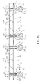
- FIG. 1 illustrates a MEMS microphone module 100 according to a first embodiment of the present invention.
- the MEMS microphone module 100 includes an application specific IC 110 , a microphone chip 120 , and a cover 130 .
- the application specific IC 110 has a first surface 111 , a second surface 112 , a plurality of first pads 113 , and a plurality of first vias 114 .
- the first pads 113 are formed on the first surface 111 of the application specific IC 110 , and the first vias 114 connected to the first pads 113 are formed to communicate with the first surface 111 and the second surface 112 .
- the microphone chip 120 has an active surface 121 , a back surface 122 , a resonant cavity 123 , a plurality of second vias 124 , a vibrating film 125 , and a plurality of second pads 126 .
- the resonant cavity 123 and the second vias 124 are formed on the back surface 122 of the microphone chip 120 , in which the resonant cavity 123 includes an opening 123 a .
- the vibrating film 125 and the second pads 126 are formed on the active surface 121 , the vibrating film 125 is disposed corresponding to the resonant cavity 123 , and the second vias 124 are connected to the second pads 126 .
- the microphone chip 120 is disposed on the first surface 111 of the application specific IC 110 with the opening 123 a of the resonant cavity 123 facing toward the application specific IC 110 , in which the first vias 114 of the application specific IC 110 are electrically connected to the second vias 124 of the microphone chip 120 .
- the application specific IC 110 also includes a first metal 115 formed in the first vias 114 and an insulator 116 formed between the first vias 114 and the first metal 115 to prevent short circuit.
- the microphone chip 120 also includes a second metal 127 and a second insulator 128 accordingly.
- the second metal 127 protrudes from the back surface 122 of the microphone chip 120 is formed in the second vias 124
- the second insulator 128 is formed between the second vias 124 and the second metal 127 to prevent short circuit.
- the MEMS microphone module 100 further includes a sealing layer 140 formed between the application specific IC 110 and the microphone chip 120 .
- the sealing layer 140 can be utilized to establish an electrical connection between the first vias 114 and the second vias 124 .
- the sealing layer 140 is preferably composed of an anisotropic conductive film or an anisotropic conductive paste.
- the sealing layer 140 utilized can be composed of a non-conductive film or a non-conductive paste.
- the cover 130 is disposed on the active surface 121 of the microphone chip 120 , in which the cover 130 includes at least one sound hole 131 .
- the cover 130 is fabricated with a “U” shaped cross-section to protect the microphone chip 120 and the vibrating film 125 .
- the MEMS microphone module 100 also has an encapsulant 150 formed between the application specific IC 110 and the microphone chip 120 .
- the encapsulant 150 is preferably disposed with respect to the exterior side of the first vias 114 of the application specific IC 110 and the second vias 124 of the microphone chip 120 .
- the encapsulant 150 could be fabricated with an “ ⁇ ” shape, a “ ⁇ ” shape, or other shapes composed of sealed-rings.
- the encapsulant 150 could be formed on the back surface 122 of the microphone chip 120 , on the first surface 111 of the application specific IC 110 , or on both the back surface 122 of the microphone chip 120 and the first surface 111 of the application specific IC 110 , which are all within the scope of the present invention.
- the encapsulant 150 is fabricated with a metal material to enhance the sealing ability for the module.
- a plurality of external pads 117 is formed on the second surface 112 of the application specific IC 110 while connecting the first vias 114 .
- the microphone module 100 further includes a plurality of solder balls 160 connected to the external pads 117 .
- the MEMS microphone module 100 would have a much smaller package size and stronger reliability.
- the present invention also eliminates the need for performing traditional wire bonding and die bonding processes, which not only reduces operating time and increases production rate, but also shortens transmission paths for the module for increasing overall transmission speed.
- FIG. 2 illustrates a cross-section of a MEMS microphone module according to another embodiment of the present invention.
- a surrounding wall 129 is formed on the active surface 121 of the microphone chip 120
- the cover 130 is disposed on the surrounding wall 129 .
- the cover 130 is fabricated with a “-” shaped cross-section.
- FIGS. 3A-3I illustrate a method for fabricating the MEMS microphone module 100 according to an embodiment of the present invention.
- a first wafer S 1 having a plurality of application specific IC 110 is provided.
- Each of the application specific IC 110 has a first surface 111 , a second surface 112 , and a plurality of first pads 113 formed on the first surface 111 .
- a plurality of first vias 114 connected to the first pads 113 is formed on the second surface 112 of the application specific IC 110 .
- the first vias 114 are formed by an etching process.
- a first metal 115 and an insulator 116 are deposited in the first vias 114 of the application specific IC 110 .
- the first insulator 116 is formed between the inner wall of the first vias 114 and the first metal 115 to prevent short circuit, and the first metal 115 is formed to protrude from the second surface 112 of the application specific IC 110 .
- the first metal 115 is preferably formed by a sputtering or electroplating process, and the first insulator 116 is preferably formed by a chemical vapor deposition process.
- a plurality of external pads 117 is formed on the second surface 112 of the application specific IC 110 , and an encapsulant 150 is formed on the first surface 111 of the application specific IC 110 .
- the encapsulant 150 is disposed with respect to the exterior side of the first vias 114 , and a plurality of solder balls 160 is bonded to the external pads 117 .
- a second wafer S 2 having a plurality of microphone chips 120 is provided.
- Each of the microphone chips 120 has an active surface 121 , a back surface 122 , a resonant cavity 123 , a plurality of second vias 124 , a vibrating film 125 , and a plurality of second pads 126 .
- the resonant cavity 123 and the second vias 124 are formed on the back surface 122 of the microphone chip 120 , in which the resonant cavity 123 also has an opening 123 a .
- the vibrating film 125 and the second pads 126 are formed on the active surface 121 , in which the vibrating film 125 is disposed corresponding to the resonant cavity 123 and the second vias 124 are connected to the second pads 126 .
- the resonant cavity 123 and the second vas 124 can be formed by an etching process.
- a surrounding wall 129 shown in FIG. 2 can be formed on the active surface 121 of the microphone chip 120 .
- a second metal 127 and a second insulator 128 are disposed into the second vias 124 of the microphone chip 120 .
- the second insulator 128 is disposed between the inner wall of the second vias 124 and the second metal 127 , and the second metal 127 is disposed to protrude from the back surface 122 of the microphone chip 120 .
- the second metal 127 is formed by a sputtering or electroplating process, and the second insulator 128 is formed by a chemical vapor deposition process.
- the encapsulant 150 is formed on the back surface 122 of the microphone chip 120 and outside the second vias 124 .
- a bonding process (such as a surface bonding process) is conducted to bond the second wafer S 2 to the first wafer S 1 .
- the microphone chip 120 of the second wafer S 2 is bonded corresponding to the application specific IC 110 of the first wafer S 1
- the opening 123 a of the resonant cavity 123 of the microphone chip 120 is positioned to face toward the application specific IC 110
- the first vias 114 of the application specific IC 110 are electrically connected to the second vias 124 of the microphone chip 120 .
- a sealing layer 140 is formed between the application specific IC 110 and the microphone chip 120 to facilitate the electrical connection between the first vias 114 and the second vias 124 .
- the sealing layer 140 is composed of an anisotropic conductive film or an anisotropic conductive paste.
- the sealing layer 140 can be composed of a non-conductive film or a non-conductive paste, which is also within the scope of the present invention.
- a cover 130 is disposed on the active surface 121 of the microphone chip 120 , in which the cover 130 includes a sound hole 131 .
- the cover 130 is fabricated with a “U” shaped cross-section.
- the cover 130 can be fabricated with a “-” shaped cross-section and disposed on a surrounding wall 129 .
- a sawing process is conducted by using a sawing tool 10 to saw the first wafer S 1 and the second wafer S 2 to form a plurality of MEMS microphone modules 100 .
Abstract
Description
Claims (10)
Applications Claiming Priority (3)
| Application Number | Priority Date | Filing Date | Title |
|---|---|---|---|
| TW095149878 | 2006-12-29 | ||
| TW095149878A TWI315295B (en) | 2006-12-29 | 2006-12-29 | Mems microphone module and method thereof |
| TW95149878A | 2006-12-29 |
Publications (2)
| Publication Number | Publication Date |
|---|---|
| US20080157238A1 US20080157238A1 (en) | 2008-07-03 |
| US7808060B2 true US7808060B2 (en) | 2010-10-05 |
Family
ID=39582644
Family Applications (1)
| Application Number | Title | Priority Date | Filing Date |
|---|---|---|---|
| US11/943,597 Active 2029-01-27 US7808060B2 (en) | 2006-12-29 | 2007-11-21 | MEMS microphone module and method thereof |
Country Status (2)
| Country | Link |
|---|---|
| US (1) | US7808060B2 (en) |
| TW (1) | TWI315295B (en) |
Cited By (29)
| Publication number | Priority date | Publication date | Assignee | Title |
|---|---|---|---|---|
| US20110233692A1 (en) * | 2008-12-12 | 2011-09-29 | Takeshi Inoda | Microphone unit and voice input device using same |
| US20120189144A1 (en) * | 2011-01-24 | 2012-07-26 | Analog Devices, Inc. | Packaged Microphone with Reduced Parasitics |
| US20120217650A1 (en) * | 2011-02-24 | 2012-08-30 | Seiko Epson Corporation | Semiconductor device, sensor and electronic device |
| US20130022223A1 (en) * | 2011-01-25 | 2013-01-24 | The Board Of Regents Of The University Of Texas System | Automated method of classifying and suppressing noise in hearing devices |
| US8446000B2 (en) | 2009-11-24 | 2013-05-21 | Chi-Chih Shen | Package structure and package process |
| US8541883B2 (en) | 2011-11-29 | 2013-09-24 | Advanced Semiconductor Engineering, Inc. | Semiconductor device having shielded conductive vias |
| US8643167B2 (en) | 2011-01-06 | 2014-02-04 | Advanced Semiconductor Engineering, Inc. | Semiconductor package with through silicon vias and method for making the same |
| US8692362B2 (en) | 2010-08-30 | 2014-04-08 | Advanced Semiconductor Engineering, Inc. | Semiconductor structure having conductive vias and method for manufacturing the same |
| US8786098B2 (en) | 2010-10-11 | 2014-07-22 | Advanced Semiconductor Engineering, Inc. | Semiconductor element having conductive vias and semiconductor package having a semiconductor element with conductive vias and method for making the same |
| US8786060B2 (en) | 2012-05-04 | 2014-07-22 | Advanced Semiconductor Engineering, Inc. | Semiconductor package integrated with conformal shield and antenna |
| US8841751B2 (en) | 2013-01-23 | 2014-09-23 | Advanced Semiconductor Engineering, Inc. | Through silicon vias for semiconductor devices and manufacturing method thereof |
| US8853819B2 (en) | 2011-01-07 | 2014-10-07 | Advanced Semiconductor Engineering, Inc. | Semiconductor structure with passive element network and manufacturing method thereof |
| US8865520B2 (en) | 2010-08-27 | 2014-10-21 | Advanced Semiconductor Engineering, Inc. | Carrier bonding and detaching processes for a semiconductor wafer |
| US8937387B2 (en) | 2012-11-07 | 2015-01-20 | Advanced Semiconductor Engineering, Inc. | Semiconductor device with conductive vias |
| US8952542B2 (en) | 2012-11-14 | 2015-02-10 | Advanced Semiconductor Engineering, Inc. | Method for dicing a semiconductor wafer having through silicon vias and resultant structures |
| US8963316B2 (en) | 2012-02-15 | 2015-02-24 | Advanced Semiconductor Engineering, Inc. | Semiconductor device and method for manufacturing the same |
| US8975157B2 (en) | 2012-02-08 | 2015-03-10 | Advanced Semiconductor Engineering, Inc. | Carrier bonding and detaching processes for a semiconductor wafer |
| US8987734B2 (en) | 2013-03-15 | 2015-03-24 | Advanced Semiconductor Engineering, Inc. | Semiconductor wafer, semiconductor process and semiconductor package |
| US9007273B2 (en) | 2010-09-09 | 2015-04-14 | Advances Semiconductor Engineering, Inc. | Semiconductor package integrated with conformal shield and antenna |
| US9024445B2 (en) | 2010-11-19 | 2015-05-05 | Advanced Semiconductor Engineering, Inc. | Semiconductor device having conductive vias and semiconductor package having semiconductor device |
| US9089268B2 (en) | 2013-03-13 | 2015-07-28 | Advanced Semiconductor Engineering, Inc. | Neural sensing device and method for making the same |
| US9153542B2 (en) | 2012-08-01 | 2015-10-06 | Advanced Semiconductor Engineering, Inc. | Semiconductor package having an antenna and manufacturing method thereof |
| US9173583B2 (en) | 2013-03-15 | 2015-11-03 | Advanced Semiconductor Engineering, Inc. | Neural sensing device and method for making the same |
| US9181086B1 (en) | 2012-10-01 | 2015-11-10 | The Research Foundation For The State University Of New York | Hinged MEMS diaphragm and method of manufacture therof |
| US9406552B2 (en) | 2012-12-20 | 2016-08-02 | Advanced Semiconductor Engineering, Inc. | Semiconductor device having conductive via and manufacturing process |
| US20170240418A1 (en) * | 2016-02-18 | 2017-08-24 | Knowles Electronics, Llc | Low-cost miniature mems vibration sensor |
| US9826316B2 (en) | 2013-05-31 | 2017-11-21 | Heptagon Micro Optics Pte. Ltd. | MEMS microphone modules and wafer-level techniques for fabricating the same |
| US9978688B2 (en) | 2013-02-28 | 2018-05-22 | Advanced Semiconductor Engineering, Inc. | Semiconductor package having a waveguide antenna and manufacturing method thereof |
| US11350220B2 (en) * | 2020-01-17 | 2022-05-31 | Sae Magnetics (H.K.) Ltd. | MEMS package, MEMS microphone and method of manufacturing the MEMS package |
Families Citing this family (40)
| Publication number | Priority date | Publication date | Assignee | Title |
|---|---|---|---|---|
| US20090194829A1 (en) * | 2008-01-31 | 2009-08-06 | Shine Chung | MEMS Packaging Including Integrated Circuit Dies |
| JP4366666B1 (en) | 2008-09-12 | 2009-11-18 | オムロン株式会社 | Semiconductor device |
| TWI508194B (en) | 2009-01-06 | 2015-11-11 | Xintec Inc | Electronic device package and fabrication method thereof |
| US8199939B2 (en) * | 2009-01-21 | 2012-06-12 | Nokia Corporation | Microphone package |
| US8739626B2 (en) * | 2009-08-04 | 2014-06-03 | Fairchild Semiconductor Corporation | Micromachined inertial sensor devices |
| TWI444052B (en) | 2009-12-17 | 2014-07-01 | Ind Tech Res Inst | Capacitive transducer and fabrication method |
| CN102196345A (en) * | 2010-03-03 | 2011-09-21 | 财团法人工业技术研究院 | Capacitance type sensor and manufacturing method thereof |
| WO2012027274A2 (en) * | 2010-08-23 | 2012-03-01 | The Regents Of The University Of California | Compositions and methods for imaging |
| DE102010040370B4 (en) * | 2010-09-08 | 2016-10-06 | Robert Bosch Gmbh | MEMS microphone package |
| KR101938609B1 (en) | 2010-09-18 | 2019-01-15 | 페어차일드 세미컨덕터 코포레이션 | Micromachined monolithic 6-axis inertial sensor |
| CN103221331B (en) * | 2010-09-18 | 2016-02-03 | 快捷半导体公司 | Hermetically sealed for MEMS |
| EP2616772B1 (en) | 2010-09-18 | 2016-06-22 | Fairchild Semiconductor Corporation | Micromachined monolithic 3-axis gyroscope with single drive |
| KR101871865B1 (en) * | 2010-09-18 | 2018-08-02 | 페어차일드 세미컨덕터 코포레이션 | Multi-die mems package |
| DE112011103124T5 (en) | 2010-09-18 | 2013-12-19 | Fairchild Semiconductor Corporation | Bearing for reducing quadrature for resonant micromechanical devices |
| US8813564B2 (en) | 2010-09-18 | 2014-08-26 | Fairchild Semiconductor Corporation | MEMS multi-axis gyroscope with central suspension and gimbal structure |
| WO2012040211A2 (en) | 2010-09-20 | 2012-03-29 | Fairchild Semiconductor Corporation | Microelectromechanical pressure sensor including reference capacitor |
| WO2012040245A2 (en) | 2010-09-20 | 2012-03-29 | Fairchild Semiconductor Corporation | Through silicon via with reduced shunt capacitance |
| CN102464294B (en) * | 2010-11-16 | 2015-02-18 | 矽品精密工业股份有限公司 | Manufacturing method for packaging structure with micro electro mechanical element |
| DE102011005676A1 (en) * | 2011-03-17 | 2012-09-20 | Robert Bosch Gmbh | component |
| US9062972B2 (en) | 2012-01-31 | 2015-06-23 | Fairchild Semiconductor Corporation | MEMS multi-axis accelerometer electrode structure |
| US8978475B2 (en) | 2012-02-01 | 2015-03-17 | Fairchild Semiconductor Corporation | MEMS proof mass with split z-axis portions |
| US8754694B2 (en) | 2012-04-03 | 2014-06-17 | Fairchild Semiconductor Corporation | Accurate ninety-degree phase shifter |
| US9488693B2 (en) | 2012-04-04 | 2016-11-08 | Fairchild Semiconductor Corporation | Self test of MEMS accelerometer with ASICS integrated capacitors |
| US8742964B2 (en) | 2012-04-04 | 2014-06-03 | Fairchild Semiconductor Corporation | Noise reduction method with chopping for a merged MEMS accelerometer sensor |
| KR102058489B1 (en) | 2012-04-05 | 2019-12-23 | 페어차일드 세미컨덕터 코포레이션 | Mems device front-end charge amplifier |
| EP2647952B1 (en) | 2012-04-05 | 2017-11-15 | Fairchild Semiconductor Corporation | Mems device automatic-gain control loop for mechanical amplitude drive |
| EP2647955B8 (en) | 2012-04-05 | 2018-12-19 | Fairchild Semiconductor Corporation | MEMS device quadrature phase shift cancellation |
| US9069006B2 (en) | 2012-04-05 | 2015-06-30 | Fairchild Semiconductor Corporation | Self test of MEMS gyroscope with ASICs integrated capacitors |
| KR101999745B1 (en) | 2012-04-12 | 2019-10-01 | 페어차일드 세미컨덕터 코포레이션 | Micro-electro-mechanical-system(mems) driver |
| US9625272B2 (en) | 2012-04-12 | 2017-04-18 | Fairchild Semiconductor Corporation | MEMS quadrature cancellation and signal demodulation |
| US9061884B1 (en) | 2012-04-24 | 2015-06-23 | Amkor Technology, Inc. | Integrated circuit with efficient MEMS architecture |
| DE102013014881B4 (en) | 2012-09-12 | 2023-05-04 | Fairchild Semiconductor Corporation | Enhanced silicon via with multi-material fill |
| US20140090485A1 (en) * | 2012-10-02 | 2014-04-03 | Robert Bosch Gmbh | MEMS Pressure Sensor Assembly |
| KR101771064B1 (en) * | 2013-06-28 | 2017-08-24 | 인텔 아이피 코포레이션 | Microelectromechanical system (mems) on application specific integrated circuit (asic) |
| US9432759B2 (en) | 2013-07-22 | 2016-08-30 | Infineon Technologies Ag | Surface mountable microphone package, a microphone arrangement, a mobile phone and a method for recording microphone signals |
| US9332330B2 (en) | 2013-07-22 | 2016-05-03 | Infineon Technologies Ag | Surface mountable microphone package, a microphone arrangement, a mobile phone and a method for recording microphone signals |
| DE102014211190A1 (en) * | 2014-06-12 | 2015-12-17 | Robert Bosch Gmbh | Micromechanical sound transducer arrangement and a corresponding manufacturing method |
| CN106612485B (en) * | 2015-10-23 | 2024-03-29 | 钰太芯微电子科技(上海)有限公司 | MEMS microphone and radio device |
| WO2017075764A1 (en) * | 2015-11-03 | 2017-05-11 | Goertek. Inc | Mems multi-module assembly, manufacturing method and electronics apparatus |
| DE102021213183A1 (en) | 2021-11-23 | 2023-05-25 | Robert Bosch Gesellschaft mit beschränkter Haftung | Sound or pressure transducer device |
Citations (6)
| Publication number | Priority date | Publication date | Assignee | Title |
|---|---|---|---|---|
| US6178249B1 (en) * | 1998-06-18 | 2001-01-23 | Nokia Mobile Phones Limited | Attachment of a micromechanical microphone |
| US20040253760A1 (en) * | 2003-06-13 | 2004-12-16 | Agency For Science, Technology And Research | Method to fabricate a highly perforated silicon diaphragm with controlable thickness and low stress |
| US20050179100A1 (en) * | 2002-05-15 | 2005-08-18 | Infineon Technologies Ag | Micromechanical capacitive transducer and method for producing the same |
| US20050189635A1 (en) * | 2004-03-01 | 2005-09-01 | Tessera, Inc. | Packaged acoustic and electromagnetic transducer chips |
| US20050207605A1 (en) * | 2004-03-08 | 2005-09-22 | Infineon Technologies Ag | Microphone and method of producing a microphone |
| US20070105304A1 (en) * | 2005-09-28 | 2007-05-10 | Junichi Kasai | Semiconductor device, fabrication method therefor, and film fabrication method |
-
2006
- 2006-12-29 TW TW095149878A patent/TWI315295B/en active
-
2007
- 2007-11-21 US US11/943,597 patent/US7808060B2/en active Active
Patent Citations (6)
| Publication number | Priority date | Publication date | Assignee | Title |
|---|---|---|---|---|
| US6178249B1 (en) * | 1998-06-18 | 2001-01-23 | Nokia Mobile Phones Limited | Attachment of a micromechanical microphone |
| US20050179100A1 (en) * | 2002-05-15 | 2005-08-18 | Infineon Technologies Ag | Micromechanical capacitive transducer and method for producing the same |
| US20040253760A1 (en) * | 2003-06-13 | 2004-12-16 | Agency For Science, Technology And Research | Method to fabricate a highly perforated silicon diaphragm with controlable thickness and low stress |
| US20050189635A1 (en) * | 2004-03-01 | 2005-09-01 | Tessera, Inc. | Packaged acoustic and electromagnetic transducer chips |
| US20050207605A1 (en) * | 2004-03-08 | 2005-09-22 | Infineon Technologies Ag | Microphone and method of producing a microphone |
| US20070105304A1 (en) * | 2005-09-28 | 2007-05-10 | Junichi Kasai | Semiconductor device, fabrication method therefor, and film fabrication method |
Cited By (39)
| Publication number | Priority date | Publication date | Assignee | Title |
|---|---|---|---|---|
| US8823115B2 (en) * | 2008-12-12 | 2014-09-02 | Funai Electric Co., Ltd. | Microphone unit and voice input device using same |
| US20110233692A1 (en) * | 2008-12-12 | 2011-09-29 | Takeshi Inoda | Microphone unit and voice input device using same |
| US8446000B2 (en) | 2009-11-24 | 2013-05-21 | Chi-Chih Shen | Package structure and package process |
| US8865520B2 (en) | 2010-08-27 | 2014-10-21 | Advanced Semiconductor Engineering, Inc. | Carrier bonding and detaching processes for a semiconductor wafer |
| US8692362B2 (en) | 2010-08-30 | 2014-04-08 | Advanced Semiconductor Engineering, Inc. | Semiconductor structure having conductive vias and method for manufacturing the same |
| US9007273B2 (en) | 2010-09-09 | 2015-04-14 | Advances Semiconductor Engineering, Inc. | Semiconductor package integrated with conformal shield and antenna |
| US8786098B2 (en) | 2010-10-11 | 2014-07-22 | Advanced Semiconductor Engineering, Inc. | Semiconductor element having conductive vias and semiconductor package having a semiconductor element with conductive vias and method for making the same |
| US9024445B2 (en) | 2010-11-19 | 2015-05-05 | Advanced Semiconductor Engineering, Inc. | Semiconductor device having conductive vias and semiconductor package having semiconductor device |
| US8643167B2 (en) | 2011-01-06 | 2014-02-04 | Advanced Semiconductor Engineering, Inc. | Semiconductor package with through silicon vias and method for making the same |
| US8853819B2 (en) | 2011-01-07 | 2014-10-07 | Advanced Semiconductor Engineering, Inc. | Semiconductor structure with passive element network and manufacturing method thereof |
| US8842859B2 (en) * | 2011-01-24 | 2014-09-23 | Invensense, Inc. | Packaged microphone with reduced parasitics |
| US20120189144A1 (en) * | 2011-01-24 | 2012-07-26 | Analog Devices, Inc. | Packaged Microphone with Reduced Parasitics |
| US9364669B2 (en) * | 2011-01-25 | 2016-06-14 | The Board Of Regents Of The University Of Texas System | Automated method of classifying and suppressing noise in hearing devices |
| US20130022223A1 (en) * | 2011-01-25 | 2013-01-24 | The Board Of Regents Of The University Of Texas System | Automated method of classifying and suppressing noise in hearing devices |
| US9209112B2 (en) | 2011-02-24 | 2015-12-08 | Seiko Epson Corporation | Semiconductor device having stacked substrates with protruding and recessed electrode connection |
| US20120217650A1 (en) * | 2011-02-24 | 2012-08-30 | Seiko Epson Corporation | Semiconductor device, sensor and electronic device |
| US9000575B2 (en) * | 2011-02-24 | 2015-04-07 | Seiko Epson Corporation | Semiconductor device having stacked substrates with protruding and recessed electrode connection |
| US8541883B2 (en) | 2011-11-29 | 2013-09-24 | Advanced Semiconductor Engineering, Inc. | Semiconductor device having shielded conductive vias |
| US8975157B2 (en) | 2012-02-08 | 2015-03-10 | Advanced Semiconductor Engineering, Inc. | Carrier bonding and detaching processes for a semiconductor wafer |
| US8963316B2 (en) | 2012-02-15 | 2015-02-24 | Advanced Semiconductor Engineering, Inc. | Semiconductor device and method for manufacturing the same |
| US8786060B2 (en) | 2012-05-04 | 2014-07-22 | Advanced Semiconductor Engineering, Inc. | Semiconductor package integrated with conformal shield and antenna |
| US9153542B2 (en) | 2012-08-01 | 2015-10-06 | Advanced Semiconductor Engineering, Inc. | Semiconductor package having an antenna and manufacturing method thereof |
| US9906869B2 (en) | 2012-10-01 | 2018-02-27 | The Research Foundation For The State University Of New York | Hinged MEMS diaphragm, and method of manufacture thereof |
| US9181086B1 (en) | 2012-10-01 | 2015-11-10 | The Research Foundation For The State University Of New York | Hinged MEMS diaphragm and method of manufacture therof |
| US9554213B2 (en) | 2012-10-01 | 2017-01-24 | The Research Foundation For The State University Of New York | Hinged MEMS diaphragm |
| US8937387B2 (en) | 2012-11-07 | 2015-01-20 | Advanced Semiconductor Engineering, Inc. | Semiconductor device with conductive vias |
| US8952542B2 (en) | 2012-11-14 | 2015-02-10 | Advanced Semiconductor Engineering, Inc. | Method for dicing a semiconductor wafer having through silicon vias and resultant structures |
| US9406552B2 (en) | 2012-12-20 | 2016-08-02 | Advanced Semiconductor Engineering, Inc. | Semiconductor device having conductive via and manufacturing process |
| US9960121B2 (en) | 2012-12-20 | 2018-05-01 | Advanced Semiconductor Engineering, Inc. | Semiconductor device having conductive via and manufacturing process for same |
| US8841751B2 (en) | 2013-01-23 | 2014-09-23 | Advanced Semiconductor Engineering, Inc. | Through silicon vias for semiconductor devices and manufacturing method thereof |
| US9728451B2 (en) | 2013-01-23 | 2017-08-08 | Advanced Semiconductor Engineering, Inc. | Through silicon vias for semiconductor devices and manufacturing method thereof |
| US9978688B2 (en) | 2013-02-28 | 2018-05-22 | Advanced Semiconductor Engineering, Inc. | Semiconductor package having a waveguide antenna and manufacturing method thereof |
| US9089268B2 (en) | 2013-03-13 | 2015-07-28 | Advanced Semiconductor Engineering, Inc. | Neural sensing device and method for making the same |
| US8987734B2 (en) | 2013-03-15 | 2015-03-24 | Advanced Semiconductor Engineering, Inc. | Semiconductor wafer, semiconductor process and semiconductor package |
| US9173583B2 (en) | 2013-03-15 | 2015-11-03 | Advanced Semiconductor Engineering, Inc. | Neural sensing device and method for making the same |
| US9826316B2 (en) | 2013-05-31 | 2017-11-21 | Heptagon Micro Optics Pte. Ltd. | MEMS microphone modules and wafer-level techniques for fabricating the same |
| US10171918B2 (en) | 2013-05-31 | 2019-01-01 | Heptagon Micro Optics Pte. Ltd. | MEMS microphone modules and wafer-level techniques for fabricating the same |
| US20170240418A1 (en) * | 2016-02-18 | 2017-08-24 | Knowles Electronics, Llc | Low-cost miniature mems vibration sensor |
| US11350220B2 (en) * | 2020-01-17 | 2022-05-31 | Sae Magnetics (H.K.) Ltd. | MEMS package, MEMS microphone and method of manufacturing the MEMS package |
Also Published As
| Publication number | Publication date |
|---|---|
| TW200827288A (en) | 2008-07-01 |
| TWI315295B (en) | 2009-10-01 |
| US20080157238A1 (en) | 2008-07-03 |
Similar Documents
| Publication | Publication Date | Title |
|---|---|---|
| US7808060B2 (en) | MEMS microphone module and method thereof | |
| US9418940B2 (en) | Structures and methods for stack type semiconductor packaging | |
| US8324728B2 (en) | Wafer level packaging using flip chip mounting | |
| US8154110B2 (en) | Double-faced electrode package and its manufacturing method | |
| TWI469233B (en) | Packaging system with hollow package | |
| US8836132B2 (en) | Vertical mount package and wafer level packaging therefor | |
| JP5215244B2 (en) | Semiconductor device | |
| US8018032B2 (en) | Silicon substrate and chip package structure with silicon base having stepped recess for accommodating chip | |
| JP5358089B2 (en) | Semiconductor device | |
| CN110677793A (en) | Microphone packaging structure | |
| JP2007027526A (en) | Dual-face electrode package and its manufacturing method | |
| JP2005294443A (en) | Semiconductor device and its manufacturing method | |
| JP2003188263A (en) | Method for producing semiconductor integrated circuit chip and semiconductor package using semiconductor integrated circuit chip | |
| JPH08306724A (en) | Semiconductor device, manufacturing method and its mounting method | |
| US20090236711A1 (en) | Method of making and designing lead frames for semiconductor packages | |
| JP2005303056A (en) | Semiconductor integrated circuit device | |
| JP6487584B1 (en) | Pressure sensor package structure | |
| US20120241937A1 (en) | Package structure having micro-electromechanical element | |
| JP2001313362A (en) | Semiconductor device | |
| JP4876818B2 (en) | Resin-sealed semiconductor device and manufacturing method thereof | |
| JP2008147368A (en) | Semiconductor device | |
| KR200148753Y1 (en) | Semiconductor package | |
| TW202312373A (en) | Compartment shielding with metal frame and cap | |
| KR100425946B1 (en) | METHOD FOR FORMING Au STUD BUMP OF FLIP CHIP PACKAGE | |
| CN112366184A (en) | Fan-out packaging structure of filter and packaging method thereof |
Legal Events
| Date | Code | Title | Description |
|---|---|---|---|
| AS | Assignment |
Owner name: ADVANCED SEMICONDUCTOR ENGINEERING, INC., TAIWAN Free format text: ASSIGNMENT OF ASSIGNORS INTEREST;ASSIGNOR:HSIAO, WEI-MIN;REEL/FRAME:020141/0827 Effective date: 20071106 |
|
| STCF | Information on status: patent grant |
Free format text: PATENTED CASE |
|
| FPAY | Fee payment |
Year of fee payment: 4 |
|
| MAFP | Maintenance fee payment |
Free format text: PAYMENT OF MAINTENANCE FEE, 8TH YEAR, LARGE ENTITY (ORIGINAL EVENT CODE: M1552) Year of fee payment: 8 |
|
| MAFP | Maintenance fee payment |
Free format text: PAYMENT OF MAINTENANCE FEE, 12TH YEAR, LARGE ENTITY (ORIGINAL EVENT CODE: M1553); ENTITY STATUS OF PATENT OWNER: LARGE ENTITY Year of fee payment: 12 |