US7807560B2 - Solder bump forming method - Google Patents
Solder bump forming method Download PDFInfo
- Publication number
- US7807560B2 US7807560B2 US12/173,985 US17398508A US7807560B2 US 7807560 B2 US7807560 B2 US 7807560B2 US 17398508 A US17398508 A US 17398508A US 7807560 B2 US7807560 B2 US 7807560B2
- Authority
- US
- United States
- Prior art keywords
- metal film
- film
- pads
- forming
- solder bump
- Prior art date
- Legal status (The legal status is an assumption and is not a legal conclusion. Google has not performed a legal analysis and makes no representation as to the accuracy of the status listed.)
- Active, expires
Links
Images


Classifications
-
- H—ELECTRICITY
- H05—ELECTRIC TECHNIQUES NOT OTHERWISE PROVIDED FOR
- H05K—PRINTED CIRCUITS; CASINGS OR CONSTRUCTIONAL DETAILS OF ELECTRIC APPARATUS; MANUFACTURE OF ASSEMBLAGES OF ELECTRICAL COMPONENTS
- H05K3/00—Apparatus or processes for manufacturing printed circuits
- H05K3/30—Assembling printed circuits with electric components, e.g. with resistor
- H05K3/32—Assembling printed circuits with electric components, e.g. with resistor electrically connecting electric components or wires to printed circuits
- H05K3/34—Assembling printed circuits with electric components, e.g. with resistor electrically connecting electric components or wires to printed circuits by soldering
- H05K3/3457—Solder materials or compositions; Methods of application thereof
- H05K3/3478—Applying solder preforms; Transferring prefabricated solder patterns
-
- B—PERFORMING OPERATIONS; TRANSPORTING
- B23—MACHINE TOOLS; METAL-WORKING NOT OTHERWISE PROVIDED FOR
- B23K—SOLDERING OR UNSOLDERING; WELDING; CLADDING OR PLATING BY SOLDERING OR WELDING; CUTTING BY APPLYING HEAT LOCALLY, e.g. FLAME CUTTING; WORKING BY LASER BEAM
- B23K1/00—Soldering, e.g. brazing, or unsoldering
- B23K1/0008—Soldering, e.g. brazing, or unsoldering specially adapted for particular articles or work
- B23K1/0016—Brazing of electronic components
-
- B—PERFORMING OPERATIONS; TRANSPORTING
- B23—MACHINE TOOLS; METAL-WORKING NOT OTHERWISE PROVIDED FOR
- B23K—SOLDERING OR UNSOLDERING; WELDING; CLADDING OR PLATING BY SOLDERING OR WELDING; CUTTING BY APPLYING HEAT LOCALLY, e.g. FLAME CUTTING; WORKING BY LASER BEAM
- B23K3/00—Tools, devices, or special appurtenances for soldering, e.g. brazing, or unsoldering, not specially adapted for particular methods
- B23K3/06—Solder feeding devices; Solder melting pans
- B23K3/0607—Solder feeding devices
- B23K3/0623—Solder feeding devices for shaped solder piece feeding, e.g. preforms, bumps, balls, pellets, droplets
-
- H—ELECTRICITY
- H01—ELECTRIC ELEMENTS
- H01L—SEMICONDUCTOR DEVICES NOT COVERED BY CLASS H10
- H01L21/00—Processes or apparatus adapted for the manufacture or treatment of semiconductor or solid state devices or of parts thereof
- H01L21/02—Manufacture or treatment of semiconductor devices or of parts thereof
- H01L21/04—Manufacture or treatment of semiconductor devices or of parts thereof the devices having at least one potential-jump barrier or surface barrier, e.g. PN junction, depletion layer or carrier concentration layer
- H01L21/48—Manufacture or treatment of parts, e.g. containers, prior to assembly of the devices, using processes not provided for in a single one of the subgroups H01L21/06 - H01L21/326
- H01L21/4814—Conductive parts
- H01L21/4846—Leads on or in insulating or insulated substrates, e.g. metallisation
- H01L21/4853—Connection or disconnection of other leads to or from a metallisation, e.g. pins, wires, bumps
-
- B—PERFORMING OPERATIONS; TRANSPORTING
- B23—MACHINE TOOLS; METAL-WORKING NOT OTHERWISE PROVIDED FOR
- B23K—SOLDERING OR UNSOLDERING; WELDING; CLADDING OR PLATING BY SOLDERING OR WELDING; CUTTING BY APPLYING HEAT LOCALLY, e.g. FLAME CUTTING; WORKING BY LASER BEAM
- B23K2101/00—Articles made by soldering, welding or cutting
- B23K2101/36—Electric or electronic devices
- B23K2101/42—Printed circuits
-
- H—ELECTRICITY
- H01—ELECTRIC ELEMENTS
- H01L—SEMICONDUCTOR DEVICES NOT COVERED BY CLASS H10
- H01L2224/00—Indexing scheme for arrangements for connecting or disconnecting semiconductor or solid-state bodies and methods related thereto as covered by H01L24/00
- H01L2224/01—Means for bonding being attached to, or being formed on, the surface to be connected, e.g. chip-to-package, die-attach, "first-level" interconnects; Manufacturing methods related thereto
- H01L2224/10—Bump connectors; Manufacturing methods related thereto
- H01L2224/15—Structure, shape, material or disposition of the bump connectors after the connecting process
- H01L2224/16—Structure, shape, material or disposition of the bump connectors after the connecting process of an individual bump connector
-
- H—ELECTRICITY
- H01—ELECTRIC ELEMENTS
- H01L—SEMICONDUCTOR DEVICES NOT COVERED BY CLASS H10
- H01L23/00—Details of semiconductor or other solid state devices
- H01L23/48—Arrangements for conducting electric current to or from the solid state body in operation, e.g. leads, terminal arrangements ; Selection of materials therefor
- H01L23/481—Internal lead connections, e.g. via connections, feedthrough structures
-
- H—ELECTRICITY
- H01—ELECTRIC ELEMENTS
- H01L—SEMICONDUCTOR DEVICES NOT COVERED BY CLASS H10
- H01L2924/00—Indexing scheme for arrangements or methods for connecting or disconnecting semiconductor or solid-state bodies as covered by H01L24/00
- H01L2924/01—Chemical elements
- H01L2924/01019—Potassium [K]
-
- H—ELECTRICITY
- H01—ELECTRIC ELEMENTS
- H01L—SEMICONDUCTOR DEVICES NOT COVERED BY CLASS H10
- H01L2924/00—Indexing scheme for arrangements or methods for connecting or disconnecting semiconductor or solid-state bodies as covered by H01L24/00
- H01L2924/01—Chemical elements
- H01L2924/01046—Palladium [Pd]
-
- H—ELECTRICITY
- H01—ELECTRIC ELEMENTS
- H01L—SEMICONDUCTOR DEVICES NOT COVERED BY CLASS H10
- H01L2924/00—Indexing scheme for arrangements or methods for connecting or disconnecting semiconductor or solid-state bodies as covered by H01L24/00
- H01L2924/01—Chemical elements
- H01L2924/01078—Platinum [Pt]
-
- H—ELECTRICITY
- H01—ELECTRIC ELEMENTS
- H01L—SEMICONDUCTOR DEVICES NOT COVERED BY CLASS H10
- H01L2924/00—Indexing scheme for arrangements or methods for connecting or disconnecting semiconductor or solid-state bodies as covered by H01L24/00
- H01L2924/01—Chemical elements
- H01L2924/01079—Gold [Au]
-
- H—ELECTRICITY
- H05—ELECTRIC TECHNIQUES NOT OTHERWISE PROVIDED FOR
- H05K—PRINTED CIRCUITS; CASINGS OR CONSTRUCTIONAL DETAILS OF ELECTRIC APPARATUS; MANUFACTURE OF ASSEMBLAGES OF ELECTRICAL COMPONENTS
- H05K2203/00—Indexing scheme relating to apparatus or processes for manufacturing printed circuits covered by H05K3/00
- H05K2203/04—Soldering or other types of metallurgic bonding
- H05K2203/041—Solder preforms in the shape of solder balls
-
- H—ELECTRICITY
- H05—ELECTRIC TECHNIQUES NOT OTHERWISE PROVIDED FOR
- H05K—PRINTED CIRCUITS; CASINGS OR CONSTRUCTIONAL DETAILS OF ELECTRIC APPARATUS; MANUFACTURE OF ASSEMBLAGES OF ELECTRICAL COMPONENTS
- H05K2203/00—Indexing scheme relating to apparatus or processes for manufacturing printed circuits covered by H05K3/00
- H05K2203/04—Soldering or other types of metallurgic bonding
- H05K2203/043—Reflowing of solder coated conductors, not during connection of components, e.g. reflowing solder paste
-
- H—ELECTRICITY
- H05—ELECTRIC TECHNIQUES NOT OTHERWISE PROVIDED FOR
- H05K—PRINTED CIRCUITS; CASINGS OR CONSTRUCTIONAL DETAILS OF ELECTRIC APPARATUS; MANUFACTURE OF ASSEMBLAGES OF ELECTRICAL COMPONENTS
- H05K2203/00—Indexing scheme relating to apparatus or processes for manufacturing printed circuits covered by H05K3/00
- H05K2203/12—Using specific substances
- H05K2203/122—Organic non-polymeric compounds, e.g. oil, wax, thiol
- H05K2203/124—Heterocyclic organic compounds, e.g. azole, furan
-
- H—ELECTRICITY
- H05—ELECTRIC TECHNIQUES NOT OTHERWISE PROVIDED FOR
- H05K—PRINTED CIRCUITS; CASINGS OR CONSTRUCTIONAL DETAILS OF ELECTRIC APPARATUS; MANUFACTURE OF ASSEMBLAGES OF ELECTRICAL COMPONENTS
- H05K3/00—Apparatus or processes for manufacturing printed circuits
- H05K3/22—Secondary treatment of printed circuits
- H05K3/24—Reinforcing the conductive pattern
- H05K3/244—Finish plating of conductors, especially of copper conductors, e.g. for pads or lands
Definitions
- the present invention relates to a solder bump forming method and more particularly to a solder bump forming method of mounting a conductive ball on each of a plurality of pads provided on a wiring board, a package such as a chip size package or a substrate such as a semiconductor chip, thereby forming the solder bump.
- FIG. 1 is a sectional view showing a related-art substrate.
- a related-art substrate 10 has a substrate body 11 , a through electrode 12 , a plurality of pads 13 and 16 , solder resists 14 and 17 , and a solder bump 19 .
- the following description will be given by taking, as an example of the substrate 10 , a wiring board to be used as a semiconductor package.
- the through electrode 12 is provided to penetrate the substrate body 11 .
- a lower end of the through electrode 12 is connected to the pad 13 and an upper end of the through electrode 12 is connected to the pad 16 .
- the through electrode 12 serves to electrically connect the pad 13 to the pad 16 .
- the pads 13 are provided on a lower surface 11 A of the substrate body 11 .
- the pads 13 have connecting portions 13 A to be external connecting terminals of the substrate 10 .
- the pads 13 are connected to the lower end of the through electrode 12 .
- the solder resist 14 is provided on the lower surface 11 A of the substrate body 11 to cover the pads 13 in parts other than the connecting portion 13 A.
- the solder resist 14 has an opening potion 14 A for exposing the connecting portion 13 A.
- the pads 16 are provided on an upper surface 11 B of the substrate body 11 .
- the pads 16 have a bump forming region 16 A.
- the bump forming region 16 A is a region where the solder bump 19 is formed and also a region where a flux for temporarily fixing a conductive ball to be the solder bump 19 onto the bump forming region 16 A is provided.
- the solder resist 17 is provided on the upper surface 11 B of the substrate body 11 to cover the pads 16 in parts other than the bump forming region 16 A.
- the solder resist 17 has an opening portion 17 A for exposing the bump forming region 16 A.
- the solder bump 19 is provided in the bump forming regions 16 A of the pads 16 .
- the solder bump 19 serves as a connecting terminal of the substrate 10 .
- the solder bump 19 is electrically connected to an electronic component (such as a semiconductor chip), for example.
- FIGS. 2 to 7 are views showing a related-art solder bump forming process.
- the same components as those of the related-art substrate 10 shown in FIG. 1 have the same reference numerals.
- a related-art solder bump forming method First of all, at a step shown in FIG. 2 , there is prepared a base material 21 having a plurality of substrate forming regions J in which a substrate 10 is to be formed, and a through electrode 12 , a plurality of pads 13 and 16 , and solder resists 14 and 17 are formed on the base material 21 by a well-known method.
- the base material 21 is cut along a cutting position K at the step shown in FIG. 7 which will be described below and is thus changed into the substrate body 11 shown in FIG. 1 .
- a flux 23 is formed to cover bump forming regions 16 A of the pads 16 . More specifically, as shown in FIG. 37 , a flux forming mask 23 A is disposed on the solder resist 17 in a state that an opening portion 23 B of the flux forming mask 23 A is aligned with the opening portion 17 A of the solder resist 17 . The flux is applied to the bump forming region 16 A via the flux forming mask 23 A by using a device for applying the flux (not shown)
- a structure shown in FIG. 3 is fixed onto a stage 25 of a conductive ball mounting device 24 , and furthermore, a conductive ball mounting mask 26 has a plurality of conductive ball mounting holes 26 A (holes for mounting conductive balls 28 on the bump forming regions 16 A of the pads 16 respectively) are disposed above the structure shown in FIG. 3 . Then, the conductive balls 28 are supplied from above the conductive ball mounting mask 26 , and the conductive ball mounting mask 26 and the stage 25 are oscillated so that the conductive ball 28 is mounted on each of the bump forming regions 16 A of the pads 16 in which the flux 23 is formed.
- the structure shown in FIG. 4 is removed from the stage 25 of the conductive ball mounting device 24 .
- the conductive ball 28 shown in FIG. 5 is subjected to a reflow treatment so that a solder bump 19 is formed on the bump forming regions 16 A of the pads 16 .
- Patent Document 1 Japanese Patent Application Publication No. 11-297886
- a variation is generated in the positions or sizes of the pad 16 and the opening portions of the solder resist 17 (the opening portion for exposing the bump forming region 16 A) over the substrate body 11 for each substrate 10 which is manufactured.
- the conductive ball mounting holes 26 A provided on the conductive ball mounting masks 26 are formed in almost designed positions.
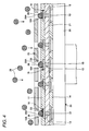
- FIG. 8 is a view for explaining problems of the related-art solder bump forming method.
- the related-art solder bump forming method has a problem in that a manufacturing cost of the substrate 10 is increased because the conductive ball mounting mask 26 is used.
- Exemplary embodiments of the present invention provide a solder bump forming method capable of reducing a manufacturing cost and reliably mounting a conductive ball on each of pads.
- An aspect of the invention is directed to a solder bump forming method of carrying out a reflow treatment over a conductive ball mounted on a plurality of pads, thereby forming a solder bump, comprising a metal film forming step of forming a metal film capable of chemically reacting to a tackifying compound on the pads, an organic sticking layer forming step of causing a solution containing the tackifying compound to chemically react to the metal film, thereby forming an organic sticking layer on the metal film, and a conductive ball mounting step of supplying the conductive ball on the organic sticking layer, thereby mounting the conductive ball on the pads through the organic sticking layer and the metal film.
- the metal film capable of chemically reacting to the tackifying compound is formed on the pads and the solution containing the tackifying compound is then caused to chemically react to the metal film to form the organic sticking layer on the metal film.
- the metal film in a part in which the organic sticking layer is formed has a small area, consequently, it is possible to form an organic sticking layer having an almost equal thickness on the metal film.
- the tackifying compound may contain at least one of a naphthotriazole based derivative, a benzotriazole based derivative, an imidazole based derivative, a benzoimidazole based derivative, a mercaptobenzothiazole based derivative and a benzothiazolethio fatty acid based derivative.
- a Cu film or an Ni film may be used for the metal film. Consequently, it is possible to cause the metal film to chemically react to the tackifying compound.
- the Ni film When the Ni film is used as the metal film, moreover, it is also possible to provide an Au layer forming step of forming an Au layer on the metal film, and an Au layer removing step of removing the Au layer immediately before the organic sticking layer forming step between the metal film forming step and the organic sticking layer forming step.
- an Au layer forming step of forming an Au layer on the metal film In the case in which the Ni film which is apt to be oxidized is used as the metal film, thus, it is possible to prevent the oxidation of the Ni film by forming the Au layer on the metal film.
- the conductive ball mounting step it is also possible to distribute the conductive balls over the pads having the organic sticking layer formed thereon and to oscillate or rock the pads, thereby mounting one of the conductive balls on each of the pads. Consequently, it is possible to mount one of the conductive balls on each of the pads.
- a diffusion preventing film forming step of forming a diffusion preventing film on the pads thus, it is possible to prevent Cu contained in the pads from being diffused into a solder bump when using Cu as a material of the pads.
- the diffusion preventing film may be constituted by at least one of an Ni film, a Pd film and an Au film which are formed by a plating method. Consequently, it is possible to prevent Cu contained in the pads from being diffused into a solder bump.
- the metal film formed on the pad is caused to carry out the chemical reaction, thereby forming the organic sticking layer for temporarily fixing the conductive ball. Therefore, it is possible to accurately dispose the fine conductive ball without using the conductive ball mounting mask. Therefore, it is possible to reduce a manufacturing cost, and furthermore, to reliably mount a conductive ball on each of the pads.
- FIG. 1 is a sectional view showing a related-art substrate
- FIG. 2 is a view (No. 1) showing a related-art solder bump forming step
- FIG. 3 is a view (No. 2) showing the related-art solder bump forming step
- FIG. 4 is a view (No. 3) showing the related-art solder bump forming step
- FIG. 5 is a view (No. 4) showing the related-art solder bump forming step
- FIG. 6 is a view (No. 5) showing the related-art solder bump forming step
- FIG. 7 is a view (No. 6) showing the related-art solder bump forming step
- FIG. 8 is a view for explaining a problem of a related-art solder bump forming method
- FIG. 9 is a sectional view showing a substrate according to a first embodiment of the invention.
- FIG. 10 is a sectional view showing a substrate according to a variant of the first embodiment of the invention.
- FIG. 11 is a view (No. 1) showing a solder bump forming step according to the first embodiment of the invention
- FIG. 12 is a view (No. 2) showing the solder bump forming step according to the first embodiment of the invention
- FIG. 13 is a view (No. 3) showing the solder bump forming step according to the first embodiment of the invention
- FIG. 14 is a view (No. 4) showing the solder bump forming step according to the first embodiment of the invention
- FIG. 15 is a view (No. 5) showing the solder bump forming step according to the first embodiment of the invention
- FIG. 16 is a view (No. 6) showing the solder bump forming step according to the first embodiment of the invention
- FIG. 17 is a view (No. 7) showing the solder bump forming step according to the first embodiment of the invention
- FIG. 18 is a view (No. 8) showing the solder bump forming step according to the first embodiment of the invention
- FIG. 19 is a view (No. 9) showing the solder bump forming step according to the first embodiment of the invention.
- FIG. 20 is a view (No. 10) showing the solder bump forming step according to the first embodiment of the invention
- FIG. 21 is a view (No. 1) showing a solder bump forming step according to a variant of the first embodiment of the invention
- FIG. 22 is a view (No. 2) showing the solder bump forming step according to the variant of the first embodiment of the invention
- FIG. 23 is a view (No. 3) showing the solder bump forming step according to the variant of the first embodiment of the invention
- FIG. 24 is a sectional view showing a substrate according to a second embodiment of the invention.
- FIG. 25 is a sectional view showing a substrate according to a variant of the second embodiment of the invention.
- FIG. 26 is a view (No. 1) showing a solder bump forming step according to the second embodiment of the invention
- FIG. 27 is a view (No. 2) showing the solder bump forming step according to the second embodiment of the invention.
- FIG. 28 is a view (No. 3) showing the solder bump forming step according to the second embodiment of the invention.
- FIG. 29 is a view (No. 4) showing the solder bump forming step according to the second embodiment of the invention.
- FIG. 30 is a view (No. 5) showing the solder bump forming step according to the second embodiment of the invention.
- FIG. 31 is a view (No. 1) showing a solder bump forming step according to a variant of the second embodiment of the invention
- FIG. 32 is a view (No. 2) showing the solder bump forming step according to the variant of the second embodiment of the invention.
- FIG. 33 is a view (No. 1) for explaining another conductive ball mounting method
- FIG. 34 is a view (No. 2) for explaining another conductive ball mounting method
- FIG. 35 is a view (No. 1) for explaining a further conductive ball mounting method
- FIG. 36 is a view (No. 2) for explaining the further conductive ball mounting method.
- FIG. 37 is a view for explaining a problem of a related-art solder bump forming method.
- FIG. 9 is a sectional view showing a substrate according to a first embodiment of the invention.
- a substrate 100 has a substrate body 101 , a through electrode 102 , a plurality of pads 103 and 107 , solder resists 104 and 108 , diffusion preventing films 105 and 109 , a metal film 111 , and a solder bump 112 .
- the following description will be given by taking, as an example of the substrate 100 , a wiring board to be used as a semiconductor package.
- the substrate body 101 takes a shape of a plate and has a plurality of through holes 115 .
- the through electrode 102 is provided in the through holes 115 .
- a lower end of the through electrode 102 is connected to the pad 103 and an upper end of the through electrode 102 is connected to the pad 107 .
- the through electrode 102 serves to electrically connect the pad 103 to the pad 107 .
- the pads 103 are provided on a lower surface 101 A of the substrate body 101 in a corresponding part to a position in which the lower end of the through electrode 102 is to be formed.
- the pads 103 take a circular shape seen on a plane and have a connecting portion 117 on which the diffusion preventing film 105 is to be formed.
- the connecting portion 117 is electrically connected to a mounting substrate (not shown) such as a mother board through the diffusion preventing film 105 , for example.
- the connecting portion 117 takes a circular shape seen on a plane.
- a thickness of the pads 103 can be set to be 15 ⁇ m, for example.
- the pads 103 can be set to have a diameter R 1 of 120 ⁇ m, for example.
- the connecting portion 117 can be set to have a diameter R 2 of 80 ⁇ m, for example.
- the planar shapes of the pad 103 and the connecting portion 117 are not restricted to shapes in the embodiment.
- the planar shapes of the pad 103 and the connecting portion 117 may be set to be a rectangle, a polygon or other shapes, for example.
- the solder resist 104 is provided on the lower surface 101 A of the substrate body 101 to cover the pads 103 in parts other than the connecting portion 117 .
- the solder resist 104 has an opening portion 118 for exposing a surface 117 A of the connecting portion 117 .
- the diffusion preventing film 105 is provided to cover the connecting portion 117 in an exposed part to the opening portion 118 .
- the diffusion preventing film 105 it is possible to use an Ni/Au laminated film having an Ni layer and an Au layer laminated on the surface 117 A of the connecting portion 117 in order, an Ni/Pd/Au laminated film having an Ni layer, a Pd layer and an Au layer laminated on the surface 117 A of the connecting portion 117 in order, a Pd/Au laminated film having a Pd layer and an Au layer laminated on the surface 117 A of the connecting portion 117 in order, and an Au layer formed on the surface 117 A of the connecting portion 117 , for example.
- an Ni layer for example, a thickness of 3 ⁇ m or more
- a Pd layer for example, a thickness of 0.1 ⁇ m or less
- an Au layer for example, a thickness of 0.01 ⁇ m to 0.5 ⁇ m
- the pads 107 are provided on the upper surface 101 B of the substrate body 101 in a corresponding part to a position in which the upper end of the through electrode 102 is to be formed.
- the pads 107 take a circular shape seen on a plane and have a connecting portion 121 on which the diffusion preventing film 109 is to be formed.
- the connecting portion 121 is electrically connected to the solder bump 112 through the diffusion preventing film 109 and the metal film 111 .
- the connecting portion 121 takes a circular shape seen on a plane.
- a thickness of the pads 107 can be set to be 15 ⁇ m, for example.
- the pads 107 can be set to have a radius R 3 of 120 ⁇ m, for example.
- the connecting portion 121 can be set to have a diameter R 4 of 80 ⁇ m, for example.
- the planar shapes of the pad 107 and the connecting portion 121 are not restricted to shapes in the embodiment.
- the planar shapes of the pad 107 and the connecting portion 121 may be set to be a rectangle, a polygon or other shapes, for example.
- the solder resist 108 is provided on the upper surface 101 B of the substrate body 101 to cover the pads 107 in parts other than the connecting portion 121 .
- the solder resist 108 has an opening portion 122 for exposing a surface 121 A of the connecting portion 121 in the pad 107 .
- the opening portion 122 takes a cylindrical shape.
- the opening portion 122 can be set to have such a diameter that only one conductive ball can be mounted thereon. In the case in which the conductive ball to be the solder bump 112 has a diameter of 90 ⁇ m, the opening portion 122 can be set to have a diameter of 80 ⁇ m, for example.
- the shape of the opening portion 122 is not restricted to the shape in the embodiment.
- the planar shape of the opening portion 122 may be set to be a rectangle, a polygon or other shapes.
- the diffusion preventing film 109 is provided to cover the surface 121 A of the connecting portion 121 exposed to the opening portion 122 .
- the diffusion preventing film 109 serves to prevent a metal component forming the pad 107 from being diffused into the solder bump 112 and to enhance a bonding property of the solder and the pad 107 .
- the diffusion preventing film 109 is particularly effective for the case in which the metal films 111 and 151 have small thicknesses and are diffused perfectly into the solder in the reflow of the conductive ball.
- the diffusion preventing film 109 it is possible to use an Ni/Au laminated film having an Ni layer and an Au layer laminated on the surface 121 A of the connecting portion 121 exposed to the opening portion 122 in order, an Ni/Pd/Au laminated film having an Ni layer, a Pd layer and an Au layer laminated on the surface 121 A of the connecting portion 121 in order, a Pd/Au laminated film having a Pd layer and an Au layer laminated on the surface 121 A of the connecting portion 121 in order, and an Au layer formed on the surface 121 A of the connecting portion 121 , for example.
- an Ni layer for example, a thickness of 3 ⁇ m or more
- a Pd layer for example, a thickness of 0.1 ⁇ m or less
- an Au layer for example, a thickness of 0.01 ⁇ m to 0.5 ⁇ m
- the metal film 111 is provided to cover a surface of the diffusion preventing film 109 at an opposite side to a surface provided in contact with the pad 107 .
- the metal film 111 can chemically react to a tackifying compound containing at least one of a naphthotriazole based derivative, a benzotriazole based derivative, an imidazole based derivative, a benzoimidazole based derivative, a mercaptobenzothiazole based derivative and a benzothiazolethio fatty acid based derivative.
- the metal film 111 serves to form an organic sticking layer for temporarily fixing, onto the metal film 111 , a conductive ball (which is changed into the solder bump 112 by carrying out the reflow treatment over the conductive ball) which will be described below through a reaction to a solution containing the tackifying compound.
- the metal film 111 it is possible to use a Cu film or an Ni film, for example.
- a thickness of the Cu film can be set to be 0.1 ⁇ m to 1.0 ⁇ m, for example.
- the metal film 111 can be formed by a plating method, for example.
- the solder bump 112 is provided on the surface of the metal film 111 at the opposite side to the surface provided in contact with the diffusion preventing film 109 .
- the solder bump 112 is electrically connected to an electronic component (not shown) such as a semiconductor chip.
- the substrate 100 having the structure described above it is possible to use a wiring board, a package such as a chip size package, or a semiconductor chip, for example.
- the whole metal film 111 is diffused into the solder in the reflow treatment for the conductive ball 129 at a step shown in FIG. 19 which will be described below. Therefore, the metal film 111 is not left after the solder bump 112 is formed.
- the metal film 111 covering the diffusion preventing film 109 is not present on a substrate 123 which is a finished member.
- FIG. 10 is a sectional view showing a substrate according to a variant of the first embodiment of the invention.
- the same components as those in the substrate 100 according to the first embodiment have the same reference numerals.
- the substrate 123 according to the variant of the first embodiment has the same structure as that of the substrate 100 except that the whole metal film 111 provided in the substrate 100 according to the first embodiment is diffused into the solder bump 112 .
- FIGS. 11 to 20 are views showing a solder bump forming process according to the first embodiment of the invention.
- the same components as those of the substrate 100 according to the first embodiment have the same reference numerals.
- solder bump forming method according to the embodiment will be described by taking, as an example, the case in which the substrate 100 according to the first embodiment is manufactured.
- a through hole 115 , a through electrode 102 and a plurality of pads 103 and 107 are formed, by a well-known method, on a base material 125 having a plurality of substrate forming regions A in which the substrate 100 is to be formed, and then, a solder resist 104 having an opening portion 118 exposing a surface 117 A of a connecting portion 117 is formed on a surface 125 A of the base material 125 and a solder resist 108 having an opening portion 122 exposing a surface 121 A of a connecting portion 121 is formed on a surface 125 B (at an opposite side to the surface 125 A) of the base material 125 .
- the base material 125 is cut in a cutting position B so that a plurality of substrate bodies 101 is obtained.
- the base material 125 it is possible to use a silicon substrate or a glass epoxy substrate, for example.
- the through electrode 102 , the pads 103 having the connecting portion 117 , and the pads 107 having the connecting portion 121 are formed by a plating method, for example.
- the through electrode 102 and the pads 103 and 107 it is possible to use a Cu film, for example.
- the pads 103 and 107 can be set to have a thickness of 15 ⁇ m, for example.
- a diameter R 1 of the pads 103 can be set to be 120 ⁇ m, for example.
- the connecting portion 117 can be set to have a diameter R 2 of 80 ⁇ m, for example.
- a diameter R 3 of the pads 107 can be set to be 120 ⁇ m, for example.
- a diameter R 4 of the connecting portion 121 can be set to be 80 ⁇ m, for example.
- the opening portion 118 is formed in such a manner that a diameter thereof is almost equal to the diameter R 2 of the connecting portion 117 .
- the opening portion 122 can be formed in such a manner that a diameter thereof is almost equal to the diameter R 4 of the connecting portion 121 , for example.
- the connecting portions 117 and 121 are subjected to a washing treatment and an activating treatment and a diffusion preventing film 105 is then formed on the surface 117 A of the connecting portion 117 by a plating method, and furthermore, a diffusion preventing film 109 is formed on the surface 121 A of the connecting portion 121 (a diffusion preventing film forming step).
- the washing and activating treatments include a degreasing treatment for the surfaces 117 A and 121 A of the connecting portions 117 and 121 , an etching treatment for the surfaces 117 A and 121 A of the connecting portions 117 and 121 subjected to the degreasing treatment, an acid washing treatment for the surfaces 117 A and 121 A of the connecting portions 117 and 121 subjected to the etching treatment, and the activating treatment for the surfaces 117 A and 121 A of the connecting portions 117 and 121 subjected to the acid washing treatment, for example.
- the diffusion preventing films 105 and 109 for example, it is possible to use an Ni/Au laminated film having an Ni layer and an Au layer laminated in order, an Ni/Pd/Au laminated film having an Ni layer, a Pd layer and an Au layer laminated in order, a Pd/Au laminated film having a Pd layer and an Au layer laminated in order, and an Au layer.
- an Ni layer for example, a thickness of 3 ⁇ m or more
- a Pd layer for example, a thickness of 0.1 ⁇ m or less
- an Au layer for example, a thickness of 0.01 ⁇ m to 0.5 ⁇ m
- a metal film 11 capable of chemically reacting to a tackifying compound containing at least one of a naphthotriazole based derivative, a benzotriazole based derivative, an imidazole based derivative, a benzoimidazole based derivative, a mercaptobenzothiazole based derivative and a benzothiazolethio fatty acid based derivative is formed to cover a surface of the diffusion preventing film 109 in an exposed part to the opening portion 122 by a plating method (a metal film forming step).
- the metal film 111 capable of chemically reacting to the tackifying compound, it is possible to use a Cu film or an Ni film, for example.
- the metal film 111 can be formed by the plating method, for example.
- the metal film 111 can be set to have a thickness of 0.1 ⁇ m to 1.0 ⁇ m, for example. By reducing the thickness of the Cu film to be the metal film 111 , thus, it is possible to lessen the influence of a Cu—Pd compound which adversely influences an electrical characteristic.
- a solution containing the tackifying compound is caused to chemically react to the metal film 111 to form an organic sticking layer 127 so as to cover the metal film 111 in the exposed part to the opening portion 122 (an organic sticking layer forming step). More specifically, the organic sticking layer 127 is formed by immersing the structure shown in FIG.
- the organic sticking layer 127 serves to temporarily fix a conductive ball 129 onto the metal film 111 at the step shown in FIG. 16 which will be described below.
- a thickness of the organic sticking layer 127 can be set to be 50 nm, for example.
- the metal film 111 capable of chemically reacting to the tackifying compound is formed on the pads 107 , and the solution containing the tackifying compound and the metal film 111 are then caused to chemically react to each other to form the organic sticking layer 127 on the metal film 111 in the exposed part to the opening portion 122 . Also in the case in which the surface of the metal film 111 on which the organic sticking layer 127 is formed has a small area, therefore, it is possible to form the organic sticking layer 127 having an almost equal thickness on the metal film 111 .
- the conductive balls are to be mounted on the pads 107 , consequently, it is possible to reliably mount the respective conductive balls on the pads 107 through the organic sticking layer 127 and the metal film 111 without using the conductive ball mounting mask 26 which has been required in the related art (see FIGS. 4 and 8 ). Moreover, the conductive ball mounting mask 26 is not required. Consequently, it is possible to reduce a manufacturing cost of the substrate 100 in which the solder bumps 112 are formed.
- the structure shown in FIG. 14 is fixed onto a stage 131 of a conductive ball supplying device 130 in such a manner that a plurality of conductive balls can be dropped onto the structure shown in FIG. 14 at a side where the organic sticking layer 127 is formed.
- the conductive ball supplying device 130 has such a structure as to have a stage 131 , an oscillating device 132 for oscillating the stage 131 , a support 133 for supporting the stage 131 through the oscillating device 132 , and a conductive ball housing 134 disposed above the stage 131 and serving to drop the conductive balls 129 (see FIG. 16 ) on the structure fixed onto the stage 131 .
- the conductive balls 129 are dropped from the conductive ball housing 134 disposed above the stage 131 and the structure including the pads 107 is oscillated (the stage 131 is oscillated) to mount one of the conductive balls 129 on each of the pads 107 in which the metal film 111 and the organic sticking layer 127 are formed (a conductive ball mounting step).
- a diameter of the conducive ball 129 can be set to be 80 ⁇ m to 90 ⁇ m, for example.
- the structure fixed onto the stage 131 is oscillated in a state in which the drop of the conductive balls 129 is stopped.
- the excessive conductive ball 129 which cannot be mounted on the metal film 111 is removed or collected from the solder resist 108 .
- the conductive balls 129 shown in FIG. 18 are subjected to a reflow treatment to form a solder bump 112 on each metal film 111 . Consequently, a structure corresponding to the substrate 100 is formed in a plurality of substrate forming regions A provided in the base material 125 .
- the organic sticking layer 127 volatilizes in the reflow treatment.
- the reflow treatment for the conductive balls 129 at the step shown in FIG. 19 is carried out without using a flux.
- the flux is not used, furthermore, a residue of the flux is not generated on a surface of the solder bump 112 or that of the substrate 100 . Therefore, it is possible to prevent a corrosion of the solder bump 112 and the pad 107 due to the flux. Consequently, it is possible to enhance an electrical connecting reliability of the substrate 100 and a semiconductor chip to be mounted on the substrate 100 and an electrical connecting reliability between the semiconductor chip and the substrate 100 .
- the metal film 111 provided on the diffusion preventing film 109 has a great thickness (which is equal to or greater than 0.5 ⁇ m, for example)
- the metal film 111 is left on the diffusion preventing film 109 as shown in FIG. 19 .
- the metal film 111 has a small thickness (which is smaller than 0.5 ⁇ m, for example)
- the metal film 111 is not left after the solder bump 112 is formed because the whole metal film 111 is diffused into the solder in the reflow treatment for the conductive ball 129 .
- the metal film 111 capable of chemically reacting to the tackifying compound is formed on the pads 107 , and the solution containing the tackifying compound and the metal film 111 are then caused to chemically react to each other to form the organic sticking layer 127 on the metal film 111 in the exposed part to the opening portion 122 . Also in the case in which the surface of the metal film 111 on which the organic sticking layer 127 is formed has a small area, therefore, it is possible to form the organic sticking layer 127 having an almost equal thickness on the metal film 111 .
- the conductive balls 129 are to be mounted on the pads 107 , consequently, it is possible to reliably mount one of the conductive balls 129 on each of the pads 107 through the organic sticking layer 127 and the metal film 111 without using the conductive ball mounting mask 26 which has been required in the related art (see FIG. 4 ). Moreover, the conductive ball mounting mask 26 is not required. Consequently, it is possible to reduce a manufacturing cost of the substrate 100 in which the solder bumps 112 are formed.
- FIGS. 21 to 23 are views showing a solder bump forming process according to a variant of the first embodiment of the invention.
- the same components as those in the structures shown in FIGS. 11 to 20 described above have the same reference numerals.
- solder bump forming method according to the variant of the embodiment will be described by taking, as an example, the case in which the substrate 100 according to the first embodiment is manufactured.
- a solder contained in a conductive ball 129 is molten by half to temporarily fix the conductive ball 129 to a pad 107 through a metal film 111 .
- the solder contained in the conductive ball 129 is molten by half to temporarily fix the conductive ball 129 to the pad 107 through the metal film 111 .
- a step shown in FIG. 22 which will be described below, therefore, it is possible to prevent the conductive ball 129 from slipping from the pad 107 when forming a flux 147 to cover the conductive ball 129 .
- the flux 147 is formed to cover a surface on a side where the conductive ball 129 of the structure shown in FIG. 21 is temporarily fixed and the conductive ball 129 .
- the flux 147 is formed by a coating process for example.
- a thickness of the flux 147 obtained after processing the step shown in FIG. 23 is smaller than that of the flux 147 provided in the structure shown in FIG. 22 .
- the flux 147 in the step shown in FIG. 23 is removed through washing. Subsequently, the processing in the step shown in FIG. 20 described above is carried out so that a plurality of substrates 100 is manufactured.
- the bump forming method in accordance with the variant of the embodiment by using the flux 147 when carrying out the reflow over the conductive ball 129 to form the solder bump 112 , it is possible to sufficiently maintain a bonding strength of the solder bump 112 and the pad 107 and a wettability of the solder. It is preferable to decide whether the solder bump forming method according to the variant of the embodiment is used depending on a composition of the solder constituting the conductive ball 129 .
- the conductive ball 129 In the case in which the flux is applied in a state in which the conductive ball 129 is simply bonded to the organic sticking layer 127 (the state shown in FIG. 18 ), moreover, the organic sticking layer 127 is dissolved by the flux so that the conductive ball 129 slips from the pad 107 . For this reason, it is preferable that the conductive ball 129 should be dissolved by half and fixed temporality as shown in FIG. 21 .
- the organic sticking layer 127 does not completely volatilize but remains. In this case, the organic sticking layer 127 is perfectly removed through the flux, resulting in an enhancement in the bonding strength of the solder by the application of the variant of the first embodiment, which is suitable.
- FIG. 24 is a sectional view showing a substrate according to a second embodiment of the invention.
- the same components as those in the substrate 100 according to the first embodiment have the same reference numerals.
- a substrate 150 according to the second embodiment has the same structure as that of the substrate 100 except that a metal film 151 is provided in place of the diffusion preventing film 109 and the metal film 111 which are provided in the substrate 100 according to the first embodiment.
- the metal film 151 is provided to cover a surface 121 A of a connecting portion 121 an opposite side to a surface provided in contact with an upper surface 101 B of the substrate body 101 .
- the metal film 151 can chemically react to the tackifying compound described in the first embodiment.
- the metal film 151 serves to react to a solution containing the tackifying compound described in the first embodiment, thereby forming an organic sticking layer for temporarily fixing a conductive ball 129 to the metal film 151 .
- a thickness of the metal film 151 can be set to be equal to or greater than 3 ⁇ m (for example, 3 ⁇ m to 8 ⁇ m), for instance.
- the substrate 150 having the structure described above it is possible to use a wiring board, a package such as a chip size package, or a semiconductor chip, for example.
- the metal film 151 has a small thickness (which is smaller than 0.5 ⁇ m, for example)
- the whole metal film 151 is diffused into the solder when a reflow treatment for the conductive ball 129 is carried out to form the solder bump 112 .
- the metal film 151 is not left after the solder bump 112 is formed.
- the metal film 151 is not present on a substrate 180 which is a finished member.
- FIG. 25 is a sectional view showing a substrate according to a variant of the second embodiment of the invention.
- the same components as those in the substrate 150 according to the second embodiment have the same reference numerals.
- a substrate 180 according to the variant of the second embodiment has the same structure as that of the substrate 150 except that the whole metal film 151 provided in the substrate 150 according to the second embodiment is diffused into the solder bump 112 .
- FIGS. 26 to 30 are views showing a solder bump forming process according to the second embodiment of the invention.
- the same components as those of the substrate 150 according to the second embodiment have the same reference numerals.
- a metal film 151 capable of chemically reacting to a tackifying compound containing at least one of a naphthotriazole based derivative, a benzotriazole based derivative, an imidazole based derivative, a benzoimidazole based derivative, a mercaptobenzothiazole based derivative and a benzothiazolethio fatty acid based derivative is formed to cover a surface 121 A of a connecting portion 121 in an exposed part to an opening portion 122 by a plating method (a metal film forming step).
- the metal film 151 capable of chemically reacting to the tackifying compound, it is possible to use an Ni film, for example.
- the metal film 151 can be set to have a thickness which is equal to or greater than 3 ⁇ m (for example, 3 ⁇ m to 8 ⁇ m, for example), for instance.
- the metal film 151 may be formed simultaneously with the formation of a diffusion preventing film 105 .
- the diffusion preventing film 105 is constituted by an Ni/Pd/Au laminated film, an Ni layer (an Ni film) is simultaneously formed on the surface 121 A in the formation of the Ni layer on a surface 117 A, and then, a Pd layer and an Au layer are sequentially formed on the surface 117 A by using the surface 121 A as a mask by the plating method so that the diffusion preventing film 105 and the metal film 151 are formed at the same time.
- a solution containing the tackifying compound is caused to chemically react to the metal film 151 to form an organic sticking layer 155 so as to cover the metal film 151 in the exposed part to the opening portion 122 (an organic sticking layer forming step). More specifically, the organic sticking layer 155 is formed by immersing the structure shown in FIG.
- the organic sticking layer 155 serves to temporarily fix a conductive ball 129 at a step shown in FIG. 29 which will be described below.
- a thickness of the organic sticking layer 155 can be set to be 50 nm, for example.
- the metal film 151 capable of chemically reacting to the tackifying compound is formed on the pads 107 , and the solution containing the tackifying compound and the metal film 151 are then caused to chemically react to each other to form the organic sticking layer 155 on the metal film 151 in the exposed part to the opening portion 122 . Also in the case in which the surface of the metal film 151 on which the organic sticking layer 155 is formed has a small area, therefore, it is possible to form the organic sticking layer 155 having an almost equal thickness on the metal film 151 .
- the conductive balls 129 are dropped from a conductive ball housing 134 disposed above a stage 131 of a conductive ball supplying device 130 and the structure including the pads 107 is oscillated (the stage 131 is oscillated) to mount one of the conductive balls 129 on each of the pads 107 in which the metal film 151 and the organic sticking layer 155 are formed (a conductive ball mounting step).
- the metal film 151 capable of chemically reacting to the tackifying compound is formed on the pads 107 , and the solution containing the tackifying compound and the metal film 151 are then caused to chemically react to each other to form the organic sticking layer 155 on the metal film 151 in the exposed part to the opening portion 122 . Also in the case in which the surface of the metal film 151 on which the organic sticking layer 155 is formed has a small area, therefore, it is possible to form the organic sticking layer 155 having an almost equal thickness on the metal film 151 .
- the conductive balls 129 are to be mounted on the pads 107 , consequently, it is possible to reliably mount one of the conductive balls 129 on each of the pads 107 through the organic sticking layer 155 and the metal film 151 without using the conductive ball mounting mask 26 which has been required in the related art (see FIGS. 4 and 8 ). Moreover, the conductive ball mounting mask 26 is not required. Consequently, it is possible to reduce a manufacturing cost of the substrate 150 in which the solder bumps 112 are formed.
- FIGS. 31 and 32 are views showing a solder bump forming process according to a variant of the second embodiment of the invention.
- an Au film 161 is formed to cover a surface of a metal film 151 exposed to an opening portion 122 by a plating method.
- an Ni film which is apt to be oxidized can be prevented from being oxidized when the Ni film is used as the metal film 151 .
- the Au film 161 shown in FIG. 31 is removed. Thereafter, the same processings as those in the steps shown in FIGS. 28 to 30 described above are carried out so that a plurality of substrates 150 is manufactured.
- FIGS. 33 and 34 are views for explaining another conductive ball mounting method and FIGS. 35 and 36 are views for explaining a further conductive ball mounting method.
- FIGS. 33 and 34 it is also possible to insert the structure shown in FIGS. 14 or 28 into a conductive ball housing 171 accommodating the conductive balls 129 and to then pull out the structure thus inserted, thereby bonding the conductive balls 129 to the organic sticking layers 127 and 155 .
- FIGS. 35 and 36 it is also possible to press the structure shown in FIG. 14 or 28 against a plate 173 having the conductive balls 129 mounted thereon, thereby bonding the conductive balls 129 to the organic sticking layers 127 and 155 and thus mounting the conductive balls 129 thereon.
- the invention can be applied to a solder bump forming method of mounting a conductive ball on each of pads provided on a wiring board, a package such as a chip size package, or a substrate such as a semiconductor chip to form a solder ball.
Abstract
Description
Claims (7)
Applications Claiming Priority (4)
| Application Number | Priority Date | Filing Date | Title |
|---|---|---|---|
| JP2007186020 | 2007-07-17 | ||
| JP2007-186020 | 2007-07-17 | ||
| JP2008125761A JP5297083B2 (en) | 2007-07-17 | 2008-05-13 | Solder bump formation method |
| JP2008-125761 | 2008-05-13 |
Publications (2)
| Publication Number | Publication Date |
|---|---|
| US20090023281A1 US20090023281A1 (en) | 2009-01-22 |
| US7807560B2 true US7807560B2 (en) | 2010-10-05 |
Family
ID=40265177
Family Applications (1)
| Application Number | Title | Priority Date | Filing Date |
|---|---|---|---|
| US12/173,985 Active 2028-12-13 US7807560B2 (en) | 2007-07-17 | 2008-07-16 | Solder bump forming method |
Country Status (1)
| Country | Link |
|---|---|
| US (1) | US7807560B2 (en) |
Families Citing this family (2)
| Publication number | Priority date | Publication date | Assignee | Title |
|---|---|---|---|---|
| US8531015B2 (en) * | 2009-03-26 | 2013-09-10 | Stats Chippac, Ltd. | Semiconductor device and method of forming a thin wafer without a carrier |
| JP7251446B2 (en) * | 2019-10-28 | 2023-04-04 | 株式会社オートネットワーク技術研究所 | Substrate with heat transfer member and method for manufacturing substrate with heat transfer member |
Citations (6)
| Publication number | Priority date | Publication date | Assignee | Title |
|---|---|---|---|---|
| JPH11297886A (en) | 1998-04-14 | 1999-10-29 | Nippon Avionics Co Ltd | Forming method of solder bump |
| US6217987B1 (en) * | 1996-11-20 | 2001-04-17 | Ibiden Co. Ltd. | Solder resist composition and printed circuit boards |
| US6365843B1 (en) * | 1997-12-29 | 2002-04-02 | Ibiden Co., Ltd. | Multilayer printed wiring board |
| US20060237225A1 (en) * | 2003-02-26 | 2006-10-26 | Takashi Kariya | Multilayer printed wiring board |
| US7224056B2 (en) * | 2003-09-26 | 2007-05-29 | Tessera, Inc. | Back-face and edge interconnects for lidded package |
| US7626829B2 (en) * | 2004-10-27 | 2009-12-01 | Ibiden Co., Ltd. | Multilayer printed wiring board and manufacturing method of the multilayer printed wiring board |
-
2008
- 2008-07-16 US US12/173,985 patent/US7807560B2/en active Active
Patent Citations (7)
| Publication number | Priority date | Publication date | Assignee | Title |
|---|---|---|---|---|
| US6217987B1 (en) * | 1996-11-20 | 2001-04-17 | Ibiden Co. Ltd. | Solder resist composition and printed circuit boards |
| US6365843B1 (en) * | 1997-12-29 | 2002-04-02 | Ibiden Co., Ltd. | Multilayer printed wiring board |
| JPH11297886A (en) | 1998-04-14 | 1999-10-29 | Nippon Avionics Co Ltd | Forming method of solder bump |
| US20060237225A1 (en) * | 2003-02-26 | 2006-10-26 | Takashi Kariya | Multilayer printed wiring board |
| US7224056B2 (en) * | 2003-09-26 | 2007-05-29 | Tessera, Inc. | Back-face and edge interconnects for lidded package |
| US7298030B2 (en) * | 2003-09-26 | 2007-11-20 | Tessera, Inc. | Structure and method of making sealed capped chips |
| US7626829B2 (en) * | 2004-10-27 | 2009-12-01 | Ibiden Co., Ltd. | Multilayer printed wiring board and manufacturing method of the multilayer printed wiring board |
Also Published As
| Publication number | Publication date |
|---|---|
| US20090023281A1 (en) | 2009-01-22 |
Similar Documents
| Publication | Publication Date | Title |
|---|---|---|
| US7851345B2 (en) | Semiconductor device and method of forming oxide layer on signal traces for electrical isolation in fine pitch bonding | |
| US7812460B2 (en) | Packaging substrate and method for fabricating the same | |
| US20080257595A1 (en) | Packaging substrate and method for manufacturing the same | |
| US20080122081A1 (en) | Method of fabricating electronic device having sacrificial anode, and electronic device fabricated by the same | |
| US20080201943A1 (en) | Electronic device substrate and its fabrication method, and electronic device and its fabrication method | |
| KR20000022103A (en) | C4 substrate contact pad which has a layer of ni-b plating | |
| US20130075145A1 (en) | Wiring substrate and method of manufacturing the same | |
| KR101609016B1 (en) | Semiconductor device and method of manufacturing substrates for semiconductor elements | |
| KR20060053087A (en) | Substrate, semiconductor device, substrate fabricating method, and semiconductor device fabricating method | |
| KR20060124576A (en) | Method of fabricating wiring board and method of fabricating semiconductor device | |
| US20080036079A1 (en) | Conductive connection structure formed on the surface of circuit board and manufacturing method thereof | |
| KR100614548B1 (en) | Fabrication method of wiring substrate for mounting semiconductor element and semiconductor device | |
| JP5297083B2 (en) | Solder bump formation method | |
| US8486760B2 (en) | Method of manufacturing substrate for flip chip and substrate for flip chip manufactured using the same | |
| KR101184108B1 (en) | Wiring board, process for producing the same, and process for manufacturing electronic device | |
| JP4458029B2 (en) | Manufacturing method of semiconductor device | |
| US7380338B2 (en) | Circuit board and manufacturing method thereof | |
| US7807560B2 (en) | Solder bump forming method | |
| US7544599B2 (en) | Manufacturing method of solder ball disposing surface structure of package substrate | |
| JP2005150417A (en) | Substrate for semiconductor device, its manufacturing method, and semiconductor device | |
| US9974166B2 (en) | Circuit board and manufacturing method thereof | |
| JPH09148331A (en) | Semiconductor integrated circuit device and method for manufacturing the same | |
| KR20040098170A (en) | Metal chip scale semiconductor package and manufacturing method thereof | |
| JP2001237338A (en) | Flip chip ball grid array substrate and method of manufacturing the same | |
| TWI743956B (en) | Chip package structure and method for forming the same |
Legal Events
| Date | Code | Title | Description |
|---|---|---|---|
| AS | Assignment |
Owner name: SHINKO ELECTRIC INDUSTRIES CO., LTD., JAPAN Free format text: ASSIGNMENT OF ASSIGNORS INTEREST;ASSIGNORS:IMAFUJI, KEI;NAKAZAWA, MASAO;SANADA, MASAKI;AND OTHERS;REEL/FRAME:021244/0790 Effective date: 20080709 |
|
| STCF | Information on status: patent grant |
Free format text: PATENTED CASE |
|
| FEPP | Fee payment procedure |
Free format text: PAYOR NUMBER ASSIGNED (ORIGINAL EVENT CODE: ASPN); ENTITY STATUS OF PATENT OWNER: LARGE ENTITY |
|
| CC | Certificate of correction | ||
| FPAY | Fee payment |
Year of fee payment: 4 |
|
| MAFP | Maintenance fee payment |
Free format text: PAYMENT OF MAINTENANCE FEE, 8TH YEAR, LARGE ENTITY (ORIGINAL EVENT CODE: M1552) Year of fee payment: 8 |
|
| MAFP | Maintenance fee payment |
Free format text: PAYMENT OF MAINTENANCE FEE, 12TH YEAR, LARGE ENTITY (ORIGINAL EVENT CODE: M1553); ENTITY STATUS OF PATENT OWNER: LARGE ENTITY Year of fee payment: 12 |