US7800237B2 - Electronic device including a component stack and connecting elements, and connecting elements, and method for producing the electronic device - Google Patents
Electronic device including a component stack and connecting elements, and connecting elements, and method for producing the electronic device Download PDFInfo
- Publication number
- US7800237B2 US7800237B2 US11/764,898 US76489807A US7800237B2 US 7800237 B2 US7800237 B2 US 7800237B2 US 76489807 A US76489807 A US 76489807A US 7800237 B2 US7800237 B2 US 7800237B2
- Authority
- US
- United States
- Prior art keywords
- contact areas
- stacked
- contact
- components
- component
- Prior art date
- Legal status (The legal status is an assumption and is not a legal conclusion. Google has not performed a legal analysis and makes no representation as to the accuracy of the status listed.)
- Expired - Fee Related, expires
Links
- 238000004519 manufacturing process Methods 0.000 title description 11
- 239000004065 semiconductor Substances 0.000 claims description 199
- 229910000838 Al alloy Inorganic materials 0.000 claims description 10
- 230000008054 signal transmission Effects 0.000 claims description 10
- 239000012790 adhesive layer Substances 0.000 claims description 5
- 229910052710 silicon Inorganic materials 0.000 claims description 4
- 239000010703 silicon Substances 0.000 claims description 4
- 239000000758 substrate Substances 0.000 claims description 4
- 229910001020 Au alloy Inorganic materials 0.000 claims description 3
- 230000005540 biological transmission Effects 0.000 claims description 3
- 239000003353 gold alloy Substances 0.000 claims description 3
- RYGMFSIKBFXOCR-UHFFFAOYSA-N Copper Chemical compound [Cu] RYGMFSIKBFXOCR-UHFFFAOYSA-N 0.000 claims description 2
- 229910052802 copper Inorganic materials 0.000 claims description 2
- 239000010949 copper Substances 0.000 claims description 2
- 238000000034 method Methods 0.000 description 17
- 235000012431 wafers Nutrition 0.000 description 15
- 239000000463 material Substances 0.000 description 12
- 238000005516 engineering process Methods 0.000 description 10
- 230000008901 benefit Effects 0.000 description 9
- 238000005530 etching Methods 0.000 description 7
- 238000000059 patterning Methods 0.000 description 6
- 238000005304 joining Methods 0.000 description 5
- 230000006870 function Effects 0.000 description 4
- 238000007639 printing Methods 0.000 description 4
- 229910000679 solder Inorganic materials 0.000 description 4
- XUIMIQQOPSSXEZ-UHFFFAOYSA-N Silicon Chemical compound [Si] XUIMIQQOPSSXEZ-UHFFFAOYSA-N 0.000 description 3
- 229910052751 metal Inorganic materials 0.000 description 3
- 239000002184 metal Substances 0.000 description 3
- 239000000853 adhesive Substances 0.000 description 2
- 230000001070 adhesive effect Effects 0.000 description 2
- 238000005275 alloying Methods 0.000 description 2
- 229910052782 aluminium Inorganic materials 0.000 description 2
- XAGFODPZIPBFFR-UHFFFAOYSA-N aluminium Chemical compound [Al] XAGFODPZIPBFFR-UHFFFAOYSA-N 0.000 description 2
- 230000015572 biosynthetic process Effects 0.000 description 2
- 230000008878 coupling Effects 0.000 description 2
- 238000010168 coupling process Methods 0.000 description 2
- 238000005859 coupling reaction Methods 0.000 description 2
- 239000007789 gas Substances 0.000 description 2
- 239000010410 layer Substances 0.000 description 2
- 239000000203 mixture Substances 0.000 description 2
- 238000012986 modification Methods 0.000 description 2
- 230000004048 modification Effects 0.000 description 2
- 238000005240 physical vapour deposition Methods 0.000 description 2
- 238000003825 pressing Methods 0.000 description 2
- 230000008569 process Effects 0.000 description 2
- 230000009467 reduction Effects 0.000 description 2
- UFHFLCQGNIYNRP-UHFFFAOYSA-N Hydrogen Chemical compound [H][H] UFHFLCQGNIYNRP-UHFFFAOYSA-N 0.000 description 1
- 239000003990 capacitor Substances 0.000 description 1
- 239000000969 carrier Substances 0.000 description 1
- 238000005234 chemical deposition Methods 0.000 description 1
- 238000010276 construction Methods 0.000 description 1
- 238000001312 dry etching Methods 0.000 description 1
- 238000004070 electrodeposition Methods 0.000 description 1
- 230000005496 eutectics Effects 0.000 description 1
- PCHJSUWPFVWCPO-UHFFFAOYSA-N gold Chemical compound [Au] PCHJSUWPFVWCPO-UHFFFAOYSA-N 0.000 description 1
- 229910052737 gold Inorganic materials 0.000 description 1
- 239000010931 gold Substances 0.000 description 1
- 239000001257 hydrogen Substances 0.000 description 1
- 229910052739 hydrogen Inorganic materials 0.000 description 1
- 239000011261 inert gas Substances 0.000 description 1
- 230000006386 memory function Effects 0.000 description 1
- 229910001092 metal group alloy Inorganic materials 0.000 description 1
- 238000001465 metallisation Methods 0.000 description 1
- TWNQGVIAIRXVLR-UHFFFAOYSA-N oxo(oxoalumanyloxy)alumane Chemical compound O=[Al]O[Al]=O TWNQGVIAIRXVLR-UHFFFAOYSA-N 0.000 description 1
- 238000001020 plasma etching Methods 0.000 description 1
- 230000001603 reducing effect Effects 0.000 description 1
- 238000007650 screen-printing Methods 0.000 description 1
- 230000008646 thermal stress Effects 0.000 description 1
- 238000001039 wet etching Methods 0.000 description 1
Images


Classifications
-
- H—ELECTRICITY
- H01—ELECTRIC ELEMENTS
- H01L—SEMICONDUCTOR DEVICES NOT COVERED BY CLASS H10
- H01L23/00—Details of semiconductor or other solid state devices
- H01L23/48—Arrangements for conducting electric current to or from the solid state body in operation, e.g. leads, terminal arrangements ; Selection of materials therefor
- H01L23/488—Arrangements for conducting electric current to or from the solid state body in operation, e.g. leads, terminal arrangements ; Selection of materials therefor consisting of soldered or bonded constructions
- H01L23/495—Lead-frames or other flat leads
- H01L23/49575—Assemblies of semiconductor devices on lead frames
-
- H—ELECTRICITY
- H01—ELECTRIC ELEMENTS
- H01L—SEMICONDUCTOR DEVICES NOT COVERED BY CLASS H10
- H01L23/00—Details of semiconductor or other solid state devices
- H01L23/28—Encapsulations, e.g. encapsulating layers, coatings, e.g. for protection
- H01L23/31—Encapsulations, e.g. encapsulating layers, coatings, e.g. for protection characterised by the arrangement or shape
- H01L23/3107—Encapsulations, e.g. encapsulating layers, coatings, e.g. for protection characterised by the arrangement or shape the device being completely enclosed
-
- H—ELECTRICITY
- H01—ELECTRIC ELEMENTS
- H01L—SEMICONDUCTOR DEVICES NOT COVERED BY CLASS H10
- H01L25/00—Assemblies consisting of a plurality of individual semiconductor or other solid state devices ; Multistep manufacturing processes thereof
- H01L25/03—Assemblies consisting of a plurality of individual semiconductor or other solid state devices ; Multistep manufacturing processes thereof all the devices being of a type provided for in the same subgroup of groups H01L27/00 - H01L33/00, or in a single subclass of H10K, H10N, e.g. assemblies of rectifier diodes
- H01L25/04—Assemblies consisting of a plurality of individual semiconductor or other solid state devices ; Multistep manufacturing processes thereof all the devices being of a type provided for in the same subgroup of groups H01L27/00 - H01L33/00, or in a single subclass of H10K, H10N, e.g. assemblies of rectifier diodes the devices not having separate containers
- H01L25/065—Assemblies consisting of a plurality of individual semiconductor or other solid state devices ; Multistep manufacturing processes thereof all the devices being of a type provided for in the same subgroup of groups H01L27/00 - H01L33/00, or in a single subclass of H10K, H10N, e.g. assemblies of rectifier diodes the devices not having separate containers the devices being of a type provided for in group H01L27/00
- H01L25/0657—Stacked arrangements of devices
-
- H—ELECTRICITY
- H01—ELECTRIC ELEMENTS
- H01L—SEMICONDUCTOR DEVICES NOT COVERED BY CLASS H10
- H01L25/00—Assemblies consisting of a plurality of individual semiconductor or other solid state devices ; Multistep manufacturing processes thereof
- H01L25/03—Assemblies consisting of a plurality of individual semiconductor or other solid state devices ; Multistep manufacturing processes thereof all the devices being of a type provided for in the same subgroup of groups H01L27/00 - H01L33/00, or in a single subclass of H10K, H10N, e.g. assemblies of rectifier diodes
- H01L25/04—Assemblies consisting of a plurality of individual semiconductor or other solid state devices ; Multistep manufacturing processes thereof all the devices being of a type provided for in the same subgroup of groups H01L27/00 - H01L33/00, or in a single subclass of H10K, H10N, e.g. assemblies of rectifier diodes the devices not having separate containers
- H01L25/07—Assemblies consisting of a plurality of individual semiconductor or other solid state devices ; Multistep manufacturing processes thereof all the devices being of a type provided for in the same subgroup of groups H01L27/00 - H01L33/00, or in a single subclass of H10K, H10N, e.g. assemblies of rectifier diodes the devices not having separate containers the devices being of a type provided for in group H01L29/00
- H01L25/074—Stacked arrangements of non-apertured devices
-
- H—ELECTRICITY
- H01—ELECTRIC ELEMENTS
- H01L—SEMICONDUCTOR DEVICES NOT COVERED BY CLASS H10
- H01L25/00—Assemblies consisting of a plurality of individual semiconductor or other solid state devices ; Multistep manufacturing processes thereof
- H01L25/50—Multistep manufacturing processes of assemblies consisting of devices, each device being of a type provided for in group H01L27/00 or H01L29/00
-
- H—ELECTRICITY
- H01—ELECTRIC ELEMENTS
- H01L—SEMICONDUCTOR DEVICES NOT COVERED BY CLASS H10
- H01L2224/00—Indexing scheme for arrangements for connecting or disconnecting semiconductor or solid-state bodies and methods related thereto as covered by H01L24/00
- H01L2224/01—Means for bonding being attached to, or being formed on, the surface to be connected, e.g. chip-to-package, die-attach, "first-level" interconnects; Manufacturing methods related thereto
- H01L2224/10—Bump connectors; Manufacturing methods related thereto
- H01L2224/15—Structure, shape, material or disposition of the bump connectors after the connecting process
- H01L2224/16—Structure, shape, material or disposition of the bump connectors after the connecting process of an individual bump connector
- H01L2224/161—Disposition
- H01L2224/16135—Disposition the bump connector connecting between different semiconductor or solid-state bodies, i.e. chip-to-chip
- H01L2224/16145—Disposition the bump connector connecting between different semiconductor or solid-state bodies, i.e. chip-to-chip the bodies being stacked
- H01L2224/16147—Disposition the bump connector connecting between different semiconductor or solid-state bodies, i.e. chip-to-chip the bodies being stacked the bump connector connecting to a bonding area disposed in a recess of the surface
-
- H—ELECTRICITY
- H01—ELECTRIC ELEMENTS
- H01L—SEMICONDUCTOR DEVICES NOT COVERED BY CLASS H10
- H01L2224/00—Indexing scheme for arrangements for connecting or disconnecting semiconductor or solid-state bodies and methods related thereto as covered by H01L24/00
- H01L2224/01—Means for bonding being attached to, or being formed on, the surface to be connected, e.g. chip-to-package, die-attach, "first-level" interconnects; Manufacturing methods related thereto
- H01L2224/10—Bump connectors; Manufacturing methods related thereto
- H01L2224/15—Structure, shape, material or disposition of the bump connectors after the connecting process
- H01L2224/16—Structure, shape, material or disposition of the bump connectors after the connecting process of an individual bump connector
- H01L2224/161—Disposition
- H01L2224/16151—Disposition the bump connector connecting between a semiconductor or solid-state body and an item not being a semiconductor or solid-state body, e.g. chip-to-substrate, chip-to-passive
- H01L2224/16221—Disposition the bump connector connecting between a semiconductor or solid-state body and an item not being a semiconductor or solid-state body, e.g. chip-to-substrate, chip-to-passive the body and the item being stacked
- H01L2224/16225—Disposition the bump connector connecting between a semiconductor or solid-state body and an item not being a semiconductor or solid-state body, e.g. chip-to-substrate, chip-to-passive the body and the item being stacked the item being non-metallic, e.g. insulating substrate with or without metallisation
- H01L2224/16237—Disposition the bump connector connecting between a semiconductor or solid-state body and an item not being a semiconductor or solid-state body, e.g. chip-to-substrate, chip-to-passive the body and the item being stacked the item being non-metallic, e.g. insulating substrate with or without metallisation the bump connector connecting to a bonding area disposed in a recess of the surface of the item
-
- H—ELECTRICITY
- H01—ELECTRIC ELEMENTS
- H01L—SEMICONDUCTOR DEVICES NOT COVERED BY CLASS H10
- H01L2224/00—Indexing scheme for arrangements for connecting or disconnecting semiconductor or solid-state bodies and methods related thereto as covered by H01L24/00
- H01L2224/01—Means for bonding being attached to, or being formed on, the surface to be connected, e.g. chip-to-package, die-attach, "first-level" interconnects; Manufacturing methods related thereto
- H01L2224/26—Layer connectors, e.g. plate connectors, solder or adhesive layers; Manufacturing methods related thereto
- H01L2224/31—Structure, shape, material or disposition of the layer connectors after the connecting process
- H01L2224/32—Structure, shape, material or disposition of the layer connectors after the connecting process of an individual layer connector
- H01L2224/321—Disposition
- H01L2224/32151—Disposition the layer connector connecting between a semiconductor or solid-state body and an item not being a semiconductor or solid-state body, e.g. chip-to-substrate, chip-to-passive
- H01L2224/32221—Disposition the layer connector connecting between a semiconductor or solid-state body and an item not being a semiconductor or solid-state body, e.g. chip-to-substrate, chip-to-passive the body and the item being stacked
- H01L2224/32245—Disposition the layer connector connecting between a semiconductor or solid-state body and an item not being a semiconductor or solid-state body, e.g. chip-to-substrate, chip-to-passive the body and the item being stacked the item being metallic
-
- H—ELECTRICITY
- H01—ELECTRIC ELEMENTS
- H01L—SEMICONDUCTOR DEVICES NOT COVERED BY CLASS H10
- H01L2224/00—Indexing scheme for arrangements for connecting or disconnecting semiconductor or solid-state bodies and methods related thereto as covered by H01L24/00
- H01L2224/01—Means for bonding being attached to, or being formed on, the surface to be connected, e.g. chip-to-package, die-attach, "first-level" interconnects; Manufacturing methods related thereto
- H01L2224/42—Wire connectors; Manufacturing methods related thereto
- H01L2224/47—Structure, shape, material or disposition of the wire connectors after the connecting process
- H01L2224/48—Structure, shape, material or disposition of the wire connectors after the connecting process of an individual wire connector
- H01L2224/4805—Shape
- H01L2224/4809—Loop shape
- H01L2224/48091—Arched
-
- H—ELECTRICITY
- H01—ELECTRIC ELEMENTS
- H01L—SEMICONDUCTOR DEVICES NOT COVERED BY CLASS H10
- H01L2224/00—Indexing scheme for arrangements for connecting or disconnecting semiconductor or solid-state bodies and methods related thereto as covered by H01L24/00
- H01L2224/01—Means for bonding being attached to, or being formed on, the surface to be connected, e.g. chip-to-package, die-attach, "first-level" interconnects; Manufacturing methods related thereto
- H01L2224/42—Wire connectors; Manufacturing methods related thereto
- H01L2224/47—Structure, shape, material or disposition of the wire connectors after the connecting process
- H01L2224/48—Structure, shape, material or disposition of the wire connectors after the connecting process of an individual wire connector
- H01L2224/481—Disposition
- H01L2224/48151—Connecting between a semiconductor or solid-state body and an item not being a semiconductor or solid-state body, e.g. chip-to-substrate, chip-to-passive
- H01L2224/48221—Connecting between a semiconductor or solid-state body and an item not being a semiconductor or solid-state body, e.g. chip-to-substrate, chip-to-passive the body and the item being stacked
- H01L2224/48245—Connecting between a semiconductor or solid-state body and an item not being a semiconductor or solid-state body, e.g. chip-to-substrate, chip-to-passive the body and the item being stacked the item being metallic
- H01L2224/48247—Connecting between a semiconductor or solid-state body and an item not being a semiconductor or solid-state body, e.g. chip-to-substrate, chip-to-passive the body and the item being stacked the item being metallic connecting the wire to a bond pad of the item
-
- H—ELECTRICITY
- H01—ELECTRIC ELEMENTS
- H01L—SEMICONDUCTOR DEVICES NOT COVERED BY CLASS H10
- H01L2224/00—Indexing scheme for arrangements for connecting or disconnecting semiconductor or solid-state bodies and methods related thereto as covered by H01L24/00
- H01L2224/01—Means for bonding being attached to, or being formed on, the surface to be connected, e.g. chip-to-package, die-attach, "first-level" interconnects; Manufacturing methods related thereto
- H01L2224/42—Wire connectors; Manufacturing methods related thereto
- H01L2224/47—Structure, shape, material or disposition of the wire connectors after the connecting process
- H01L2224/48—Structure, shape, material or disposition of the wire connectors after the connecting process of an individual wire connector
- H01L2224/484—Connecting portions
- H01L2224/4847—Connecting portions the connecting portion on the bonding area of the semiconductor or solid-state body being a wedge bond
- H01L2224/48472—Connecting portions the connecting portion on the bonding area of the semiconductor or solid-state body being a wedge bond the other connecting portion not on the bonding area also being a wedge bond, i.e. wedge-to-wedge
-
- H—ELECTRICITY
- H01—ELECTRIC ELEMENTS
- H01L—SEMICONDUCTOR DEVICES NOT COVERED BY CLASS H10
- H01L2224/00—Indexing scheme for arrangements for connecting or disconnecting semiconductor or solid-state bodies and methods related thereto as covered by H01L24/00
- H01L2224/73—Means for bonding being of different types provided for in two or more of groups H01L2224/10, H01L2224/18, H01L2224/26, H01L2224/34, H01L2224/42, H01L2224/50, H01L2224/63, H01L2224/71
- H01L2224/732—Location after the connecting process
- H01L2224/73251—Location after the connecting process on different surfaces
- H01L2224/73265—Layer and wire connectors
-
- H—ELECTRICITY
- H01—ELECTRIC ELEMENTS
- H01L—SEMICONDUCTOR DEVICES NOT COVERED BY CLASS H10
- H01L2224/00—Indexing scheme for arrangements for connecting or disconnecting semiconductor or solid-state bodies and methods related thereto as covered by H01L24/00
- H01L2224/80—Methods for connecting semiconductor or other solid state bodies using means for bonding being attached to, or being formed on, the surface to be connected
- H01L2224/81—Methods for connecting semiconductor or other solid state bodies using means for bonding being attached to, or being formed on, the surface to be connected using a bump connector
- H01L2224/8112—Aligning
- H01L2224/81136—Aligning involving guiding structures, e.g. spacers or supporting members
- H01L2224/81138—Aligning involving guiding structures, e.g. spacers or supporting members the guiding structures being at least partially left in the finished device
- H01L2224/81141—Guiding structures both on and outside the body
-
- H—ELECTRICITY
- H01—ELECTRIC ELEMENTS
- H01L—SEMICONDUCTOR DEVICES NOT COVERED BY CLASS H10
- H01L2224/00—Indexing scheme for arrangements for connecting or disconnecting semiconductor or solid-state bodies and methods related thereto as covered by H01L24/00
- H01L2224/80—Methods for connecting semiconductor or other solid state bodies using means for bonding being attached to, or being formed on, the surface to be connected
- H01L2224/81—Methods for connecting semiconductor or other solid state bodies using means for bonding being attached to, or being formed on, the surface to be connected using a bump connector
- H01L2224/8119—Arrangement of the bump connectors prior to mounting
- H01L2224/81191—Arrangement of the bump connectors prior to mounting wherein the bump connectors are disposed only on the semiconductor or solid-state body
-
- H—ELECTRICITY
- H01—ELECTRIC ELEMENTS
- H01L—SEMICONDUCTOR DEVICES NOT COVERED BY CLASS H10
- H01L2225/00—Details relating to assemblies covered by the group H01L25/00 but not provided for in its subgroups
- H01L2225/03—All the devices being of a type provided for in the same subgroup of groups H01L27/00 - H01L33/648 and H10K99/00
- H01L2225/04—All the devices being of a type provided for in the same subgroup of groups H01L27/00 - H01L33/648 and H10K99/00 the devices not having separate containers
- H01L2225/065—All the devices being of a type provided for in the same subgroup of groups H01L27/00 - H01L33/648 and H10K99/00 the devices not having separate containers the devices being of a type provided for in group H01L27/00
- H01L2225/06503—Stacked arrangements of devices
- H01L2225/06513—Bump or bump-like direct electrical connections between devices, e.g. flip-chip connection, solder bumps
-
- H—ELECTRICITY
- H01—ELECTRIC ELEMENTS
- H01L—SEMICONDUCTOR DEVICES NOT COVERED BY CLASS H10
- H01L2225/00—Details relating to assemblies covered by the group H01L25/00 but not provided for in its subgroups
- H01L2225/03—All the devices being of a type provided for in the same subgroup of groups H01L27/00 - H01L33/648 and H10K99/00
- H01L2225/04—All the devices being of a type provided for in the same subgroup of groups H01L27/00 - H01L33/648 and H10K99/00 the devices not having separate containers
- H01L2225/065—All the devices being of a type provided for in the same subgroup of groups H01L27/00 - H01L33/648 and H10K99/00 the devices not having separate containers the devices being of a type provided for in group H01L27/00
- H01L2225/06503—Stacked arrangements of devices
- H01L2225/06527—Special adaptation of electrical connections, e.g. rewiring, engineering changes, pressure contacts, layout
-
- H—ELECTRICITY
- H01—ELECTRIC ELEMENTS
- H01L—SEMICONDUCTOR DEVICES NOT COVERED BY CLASS H10
- H01L24/00—Arrangements for connecting or disconnecting semiconductor or solid-state bodies; Methods or apparatus related thereto
- H01L24/01—Means for bonding being attached to, or being formed on, the surface to be connected, e.g. chip-to-package, die-attach, "first-level" interconnects; Manufacturing methods related thereto
- H01L24/42—Wire connectors; Manufacturing methods related thereto
- H01L24/47—Structure, shape, material or disposition of the wire connectors after the connecting process
- H01L24/48—Structure, shape, material or disposition of the wire connectors after the connecting process of an individual wire connector
-
- H—ELECTRICITY
- H01—ELECTRIC ELEMENTS
- H01L—SEMICONDUCTOR DEVICES NOT COVERED BY CLASS H10
- H01L2924/00—Indexing scheme for arrangements or methods for connecting or disconnecting semiconductor or solid-state bodies as covered by H01L24/00
- H01L2924/0001—Technical content checked by a classifier
- H01L2924/00014—Technical content checked by a classifier the subject-matter covered by the group, the symbol of which is combined with the symbol of this group, being disclosed without further technical details
-
- H—ELECTRICITY
- H01—ELECTRIC ELEMENTS
- H01L—SEMICONDUCTOR DEVICES NOT COVERED BY CLASS H10
- H01L2924/00—Indexing scheme for arrangements or methods for connecting or disconnecting semiconductor or solid-state bodies as covered by H01L24/00
- H01L2924/01—Chemical elements
- H01L2924/01079—Gold [Au]
-
- H—ELECTRICITY
- H01—ELECTRIC ELEMENTS
- H01L—SEMICONDUCTOR DEVICES NOT COVERED BY CLASS H10
- H01L2924/00—Indexing scheme for arrangements or methods for connecting or disconnecting semiconductor or solid-state bodies as covered by H01L24/00
- H01L2924/013—Alloys
- H01L2924/0132—Binary Alloys
- H01L2924/01322—Eutectic Alloys, i.e. obtained by a liquid transforming into two solid phases
-
- H—ELECTRICITY
- H01—ELECTRIC ELEMENTS
- H01L—SEMICONDUCTOR DEVICES NOT COVERED BY CLASS H10
- H01L2924/00—Indexing scheme for arrangements or methods for connecting or disconnecting semiconductor or solid-state bodies as covered by H01L24/00
- H01L2924/15—Details of package parts other than the semiconductor or other solid state devices to be connected
- H01L2924/181—Encapsulation
-
- H—ELECTRICITY
- H01—ELECTRIC ELEMENTS
- H01L—SEMICONDUCTOR DEVICES NOT COVERED BY CLASS H10
- H01L2924/00—Indexing scheme for arrangements or methods for connecting or disconnecting semiconductor or solid-state bodies as covered by H01L24/00
- H01L2924/19—Details of hybrid assemblies other than the semiconductor or other solid state devices to be connected
- H01L2924/1901—Structure
- H01L2924/1904—Component type
- H01L2924/19041—Component type being a capacitor
-
- H—ELECTRICITY
- H01—ELECTRIC ELEMENTS
- H01L—SEMICONDUCTOR DEVICES NOT COVERED BY CLASS H10
- H01L2924/00—Indexing scheme for arrangements or methods for connecting or disconnecting semiconductor or solid-state bodies as covered by H01L24/00
- H01L2924/30—Technical effects
- H01L2924/301—Electrical effects
- H01L2924/30107—Inductance
-
- H—ELECTRICITY
- H01—ELECTRIC ELEMENTS
- H01L—SEMICONDUCTOR DEVICES NOT COVERED BY CLASS H10
- H01L2924/00—Indexing scheme for arrangements or methods for connecting or disconnecting semiconductor or solid-state bodies as covered by H01L24/00
- H01L2924/30—Technical effects
- H01L2924/301—Electrical effects
- H01L2924/3011—Impedance
Definitions
- the invention relates to an electronic device (e.g., a semiconductor device) comprising a chip stack and connecting elements.
- a semiconductor component comprising a semiconductor chip stack in which semiconductor chips are arranged with their top sides lying opposite is known. Between the two top sides of the semiconductor chips stacked one on top of another, metallic leads are arranged on an intermediate carrier connecting the contact areas of the base semiconductor chip to the contact areas of the stacked semiconductor chip. Consequently, for stacking purposes, the leads have to be bonded by their lead ends on the contact areas of the semiconductor chips to be stacked one on top of another, which can lead to problems at least during the bonding of the stacked semiconductor chips on the lead ends. It is furthermore disadvantageous that a special lead frame has to be produced for the stacking of the semiconductor chips whose top sides are oriented to one another, where the costs for producing a semiconductor component of this type rise.
- a semiconductor component includes a semiconductor component comprising semiconductor chips that are stacked one on top of another with their top sides lying opposite.
- the top sides have contact areas and external contacts in the form of solder balls which are soldered onto one another in order to realize a semiconductor chip stack for the semiconductor component.
- a semiconductor component of this type has the disadvantage that the solder balls as flip-chip contacts increase the device height and the further disadvantage that the orientation of the semiconductor chips with respect to one another is complicated and can lead to incorrect connections, especially as a reliable meeting of flip-chip contacts of the semiconductor chips to be stacked one on top of another is extremely difficult and appears to be relatively unsuitable for mass production.
- the present invention provides an electronic device (e.g., a semiconductor device) comprising a component stack (e.g., a semiconductor chip stack) and connecting elements which achieve a number of different advantages and can be configured to overcome a number of disadvantages including, without limitation, the disadvantages noted above.
- the present invention further provides connecting elements which can be suitably configured to enable a reliable and cost-effectively producible stacking of chips for an electronic device comprising a chip stack.
- an electronic device e.g., a semiconductor device
- a stack of electronic components or a component stack e.g., a semiconductor chip stack
- the component stack includes two electronic components (e.g., semiconductor chips) which are stacked one on top of another by their top sides and on the top sides of which contact areas are arranged.
- the contact areas include external contact structures as connecting elements, wherein the external contact structures on the contact areas include rib and/or trench structures. These rib and/or trench structures of stacked chips are oriented with respect to one another in such a way that the rib and/or trench structures of the contact areas of the two chips stacked one on top of another by their top sides cross one another.
- a method for producing an electronic device comprising a stack of electronic components or a component stack (e.g., a semiconductor chip stack) includes the following method steps. Wafers are produced including a plurality of device positions (e.g., semiconductor device positions), wherein the device positions include contact areas on the top side of the wafers. This is followed by patterning the contact areas with external contact structures by etching trench structures into the contact area material and/or applying rib structures to the contact areas. The wafers can then either be separated into individual components (e.g., semiconductor chips), or individual components are stacked on a base wafer in device positions and only afterward is the base wafer separated into component stacks.
- the wafer for the base component can also be a carrier without an active function, for example, to connect a plurality of stacked components in a system housing on the base component, or in order to achieve a so-called “fan out” with the base component.
- FIG. 1A shows a schematic plan view of a contact area with external contact structure of a power semiconductor chip to be stacked for a power semiconductor chip stack.
- FIG. 1B shows a schematic side view of the external contact structure of the semiconductor chip of FIG. 1A .
- FIG. 2A shows a schematic plan view of a contact area with external contact structure of a base chip for the power semiconductor chip stack.
- FIG. 2B shows a schematic side view of the external contact structure of the base chip of FIG. 2A .
- FIG. 3 shows a schematic cross section through a power semiconductor chip stack formed with the chips of FIGS. 1 and 2 .
- FIG. 4A shows a schematic plan view of a contact area with external contact structure of a power semiconductor chip to be stacked for a power semiconductor chip stack of a second embodiment.
- FIG. 4B shows a schematic side view of the external contact structure of the semiconductor chip of FIG. 4A .
- FIG. 5A shows a schematic plan view of a contact area with external contact structure of a base chip for a power semiconductor chip stack of the second embodiment.
- FIG. 5B shows a schematic side view of the external contact structure of the base chip of FIG. 5A .
- FIG. 6 shows a schematic cross section through a power semiconductor chip stack formed with the chips of FIGS. 4 and 5 .
- FIG. 7A shows in schematic plan view of a semiconductor chip to be stacked with a plurality of contact areas for the signal transmission of a semiconductor chip stack of a third embodiment.
- FIG. 7B shows a schematic side view of the semiconductor chip of FIG. 7A .
- FIG. 8A shows a schematic plan view of a base chip with a plurality of contact areas of a semiconductor chip stack for signal transmission in accordance with the third embodiment.
- FIG. 8B shows a schematic side view of the base chip of FIG. 8A .
- FIG. 9 shows a schematic cross section through a semiconductor chip stack formed with the chips of FIGS. 7 and 8 .
- FIG. 10A shows a schematic plan view of a semiconductor chip to be stacked with contact areas for a semiconductor chip stack of a fourth embodiment.
- FIG. 10B shows a schematic side view of the semiconductor chip of FIG. 10A .
- FIG. 11A shows a schematic plan view of a base chip with contact areas for a semiconductor chip stack in accordance with the fourth embodiment.
- FIG. 11B shows a schematic side view of the base chip of FIG. 11A .
- FIG. 12 shows a schematic cross section through a semiconductor chip stack formed with the chips of FIGS. 10 and 11 .
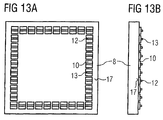
- FIG. 13A shows a schematic plan view of a semiconductor chip to be stacked of a semiconductor chip stack of a fifth embodiment.
- FIG. 13B shows a schematic side view of the semiconductor chip of FIG. 13A .
- FIG. 14 shows a schematic plan view of a base chip with contact areas for a semiconductor chip stack in accordance with the fifth embodiment.
- FIG. 15 shows a schematic cross section through a semiconductor chip stack formed with the chips of FIGS. 13 and 14 .
- FIG. 16 shows a schematic plan view of a contact connection area pattern in which not all the patterned contact areas are led toward the outside.
- FIG. 17 shows a schematic plan view of a meandering rib structure of a contact area.
- FIG. 18 shows a schematic cross section through a contact area with a trench structure etched throughout.
- FIG. 19 shows a schematic cross section through a contact area with a partially introduced trench structure.
- An electronic device such as a semiconductor device, comprising a stack of electronic components or a component stack (e.g., a semiconductor chip stack) and connecting elements.
- a component stack e.g., a semiconductor chip stack
- connecting elements e.g., a semiconductor chip stack
- the exemplary embodiments described herein are in relation to semiconductor devices with stacked semiconductor chips. However, it is noted that the invention is not limited to the exemplary embodiments, but rather encompasses any electronic devices with stacked electronic components.
- a semiconductor chip stack includes two semiconductor chips which are stacked one on top of another by their top sides and on the top sides of which contact areas are arranged.
- the contact areas include external contact structures as connecting elements, wherein the external contact structures on the contact areas include rib and/or trench structures.
- These rib and/or trench structures of stacked semiconductor chips are oriented with respect to one another in such a way that the rib and/or trench structures of the contact areas of the two semiconductor chips stacked one on top of another by their top sides cross one another.
- the semiconductor chip stack is provided with a reliable and stable connection between the contact areas since, on account of the rib and/or trench structure of the external contact structures of the two semiconductor chips, a high tolerance range is provided for the orientation of the semiconductor chips with respect to one another, such that manufacturing tolerances in semiconductor chip production cannot lead to failures during stacking. Moreover, reliable cohesive connections arise at the crossover points of the rib structure between the two stacked semiconductor chips, and enable a low-impedance coupling of the two semiconductor chips one above another.
- SiP System in Package
- SoC System on Chip
- chip technologies can be combined with a base chip by stacking, such as HF chips, sensor chips, power chips, MEM chips, chips with a different voltage supply, chips for analog processes stacked on base chips for digital processes, and vice versa, memory chips such as RAM, ROM, flash on analog and/or digital chips. Furthermore, it is possible also to stack passive components on the base chip.
- contact areas on the chip Independently of the surface structure of the contact areas, it is possible to arrange contact areas on the chip to be stacked in a manner distributed annularly, linearly or nonuniformly on a chip surface. It is advantageously possible to stack a plurality of semiconductor chips and/or passive components onto a base chip to form a circuit module.
- This type of stacking with direct contact of the contact areas using rib structures of this type is particularly advantageous for the area of application of extremely high frequency technologies.
- no lines whatsoever are required in order to connect a base semiconductor chip to the contact areas of a stacked semiconductor chip of the extremely high frequency technology by means of contact areas prepared in this way.
- the angle at which the rib and/or trench structures on the contact areas of the two semiconductor chips stacked one on top of another by their top sides are oriented with respect to one another preferably lies between 0° ⁇ 90°. This angle ensures that crossover points form whose area of contact becomes smaller as the angle increases.
- semiconductor chips for signal processing are stacked one on top of another.
- the semiconductor chips have a multiplicity of contact areas for signal transmission, wherein the two semiconductor chips stacked one on top of another by their top sides have at least per contact area one rib as external contact structure which is arranged diagonally on a square or rectangular contact area.
- the diagonal arrangement is associated with the advantage that it is thereby possible to realize the greatest possible length of a rib on a contact area.
- the contact areas are provided for power transmission of the two semiconductor chips stacked one on top of another by their top sides, then said contact areas have a multiplicity of crossing ribs as external contact structure. Since the areal extent of the contact areas is relatively large in the case of power transmission, it is also possible to realize a high number of crossing ribs in such a stack of power semiconductor chips.
- the contact areas and/or the external contact structures of the two semiconductor chips stacked one on top of another by their top sides can include an aluminum alloy comprising alloying elements, the alloying elements preferably comprising silicon and/or copper.
- the aluminum is relatively soft and ductile, with the result that an intimate intermeshing is possible upon pressing together the ribs made from an aluminum alloy.
- the rib structure makes it possible, particularly in the case of a thermosonic bonding method, for the thin unavoidable aluminum oxide skin to be rubbed down relatively without any problems, so that the aluminum alloys can fuse together at the crossover points.
- the contact areas and/or the external contact structures of a base chip of the semiconductor chip stack stacked one on top of another by their top sides have an aluminum alloy and the contact areas and/or the external contact structures of the stacked semiconductor chip have a gold alloy.
- This combination of gold alloy and aluminum alloy has the advantage that at low temperature a eutectic melt forms during bonding or during joining from gold and aluminum, which is associated with the advantage that the crossed structures are electrically connected via a eutectically fused metal alloy.
- the external contact structures can include ribs having a conical or tapered cross section, such that the cross section becomes wider toward the base of the ribs (i.e., the side walls of each tapered contact structure are nonparallel with respect to each other such that the cross-sectional profile of the contact structure tapers from the base of the contact structure to a free end of the contact structure).
- the tapered external contact structure configuration results in an area of contact at the start of a joining operation between the ribs lying one on top of another at the crossover point being small so as to facilitate the joining of the external contact structures.
- the height h with which the external contact structures project beyond the contact areas lies between 0.05 ⁇ m ⁇ h ⁇ 100 ⁇ m preferably between 0.1 ⁇ m ⁇ h ⁇ 5 ⁇ m.
- the semiconductor device can be used for extremely high frequency circuits, especially as there is no need for long connecting lines or connecting elements in order to electrically connect a semiconductor chip for extremely high frequencies to a semiconductor chip with control, supply, logic and/or memory functions. Since the areal extent of the semiconductor chip for extremely high frequency components is significantly smaller in comparison with a base chip of the semiconductor chip stack with control, supply, logic and/or memory circuits, the semiconductor chip for an extremely high frequency circuit can be introduced in that region on the base chip which is intended to be operatively connected to the semiconductor chip for extremely high frequency applications. This need not necessarily be the center of a base chip, but rather may in many applications also mean an eccentric position on the base semiconductor chip.
- a further use of a semiconductor device of this type is afforded for FET power switches and/or FET bridge circuits, wherein the large-area contact regions of a source connection or of a drain connection enable external contact structures on the contact areas with a multiplicity of ribs.
- An exemplary method for producing an electronic device such as a semiconductor device comprising a semiconductor chip stack includes the following method steps.
- the first step involves producing wafers including a plurality of semiconductor device positions, wherein the semiconductor device positions have contact areas on the top side of the wafers. This is followed by patterning the contact areas with external contact structures by etching trench structures into the contact area material and/or applying rib structures to the contact areas.
- the wafers can then either be separated into individual semiconductor chips, or individual semiconductor chips are stacked on a base wafer in semiconductor device positions and only afterward is the base wafer separated into chip stacks.
- the wafer for the base chip can also be a carrier without an active function, for example, to connect a plurality of stacked semiconductor chips in a system housing on the base chip, or to achieve a so-called “fan out” with the base chip.
- Semiconductor chips can subsequently be stacked one on top of another by their top sides, wherein the external contact structures are oriented in such a way that they cross one another or intermesh and join cohesively to one another with application of pressure.
- the chip stacks of semiconductor chips are electrically connected to a device substrate or a lead frame.
- the semiconductor chip stack can then be incorporated by means of device substrate or lead frame into a housing to form a semiconductor device or remain unencapsulated as an open module.
- This method provides a number of advantages including, without limitation, the advantage that it is possible to produce cost-effectively chip stacks that are connected to one another without the use of solder balls or interposed lead carriers. Rather, the contact areas prepared with rib or trench structures are cohesively connected to one another directly by the crossover points of the crossing ribs. Alongside stacked chips, it is also possible to apply to the base chip other components, such as resistors, inductances or capacitors, which can additionally be operatively connected to the base chip by other connecting technologies, such as bonding wires.
- a multiplicity of contact areas can be prepared correspondingly before the semiconductor chip stacks are produced by joining the external contact structures on contact areas.
- One possibility for patterning comprises etching trenches into the contact material of the contact areas. Wet etching techniques and dry etching techniques are available for such etching of trenches, plasma etching preferably being used, in which an anisotropic removal of the contact area material to be etched takes place and it is thus possible to produce extremely narrow ribs from the contact area material.
- a further possibility for producing rib structures on the contact areas comprises producing a metal layer by a PVD method (physical vapor deposition), preferably made from an aluminum alloy onto the contact areas with subsequent etching or subsequent laser removal for patterning the ribs.
- a metal layer by a PVD method (physical vapor deposition), preferably made from an aluminum alloy onto the contact areas with subsequent etching or subsequent laser removal for patterning the ribs.
- the etching of the applied metal layer can be achieved in the same way as above during the production of trenches in the contact area material.
- the laser removal technique has the advantage of an anisotropic removal of the material.
- the rib structures are produced using printing methods, such as screen printing methods, stencil printing methods and/or jet printing methods.
- the resultant ribs cannot be patterned as finely as in the case of anisotropic etching methods and/or during the anisotropic laser removal, but printing methods of this type permit a high throughput and hence mass production of correspondingly patterned contact areas on a semiconductor wafer, preferably a power semiconductor wafer.
- the contact areas When stacking the two semiconductor chips by their top sides, the contact areas can be oriented with the crossing rib structures to one another and cohesively connecting the rib structures to one another in the region of crossover points at elevated pressure and elevated temperature.
- the elevated temperature improves the intensive cohesive bond between the two contact area structures and thus increases the reliability of the semiconductor device and its service life.
- the semiconductor chips are coated prior to stacking with an adhesive composition in such a way that the rib structures of the external contact structures are uncovered and project from the adhesive layer.
- care is taken to ensure that the projecting external contact structures intermesh during stacking in such a way that the adhesive layers can additionally form a cohesive connection with one another.
- the relatively narrow interspace between the stacked semiconductor chip and the base semiconductor chip is completely filled by the adhesive layer, and the reliability of the electrical connection between the stacked semiconductor chips is additionally improved by a large-area adhesive zone.
- a semiconductor base chip whose areal extent is greater than the areal extent of the stacked semiconductor chip can be used for the semiconductor chip stack.
- the larger area of the base chip has contact areas outside the stack region of the stacked semiconductor chip. These contact areas on the edge regions of the base semiconductor chip can then be electrically connected to the device substrate via connecting elements.
- This construction is advantageous since the stacked semiconductor chip is completely supported by the base semiconductor chip.
- the same semiconductor material, such as silicon can be used for the base semiconductor chip and the stacked semiconductor chip, with the result that there are no thermal stress problems either, which problems occur when semiconductor chips are connected to one another by circuit boards or are electrically connected to one another by an interposer.
- FIG. 1A shows a schematic plan view of a contact area 10 with external contact structure 12 of a power semiconductor chip 8 to be stacked.
- FIG. 1B shows the corresponding side view of the semiconductor chip 8 with the patterned contact area 10 on the top side 17 of the power semiconductor chip 8 .
- Power semiconductor chips of this type have contact areas 10 , such as a drain connection area, a source connection area, an emitter connection area and/or a collector connection area, which in terms of their areal extent cover one side of the power semiconductor chip 8 in part or completely.
- the contact areas 10 to be stacked one on top of another have ribs 13 , which cover the contact area 10 of the stacked semiconductor chip 8 in strip-type fashion and in this case project with a height h above the contact area 10 .
- FIG. 2A shows a schematic plan view of a contact area 9 with external contact structure 11 of a base chip 7 for the power semiconductor device stack of the first embodiment of the invention.
- FIG. 2B shows in respect of this the side view of the base chip 7 with contact area 9 and longitudinal ribs 13 , the longitudinal ribs likewise projecting with a height h above the contact area 9 .
- the height h lies between in micrometers 0.5 ⁇ m ⁇ h ⁇ 50 ⁇ m.
- the ribs 13 are displaced transverse (e.g., by an angle ⁇ of 90°) relative to the orientation of the ribs 13 in FIG. 1A , with the result that, when the semiconductor chips 7 and 8 are stacked, crossover or intersection points arise which intensively intermesh and cause the material of the ribs 13 to be joined cohesively into one another.
- a soft metal such as an aluminum alloy, is preferably used for these contact areas 9 and 10 with external contact structure 11 and 12 , such that, even at low contact pressure, the ribs 13 deform at the crossover or intersection points and produce a cohesive connection.
- This cohesive connection can be supported and improved by increasing the temperature, preferably in an inert gas furnace or else in a furnace which is flushed with forming gas and the atmosphere of which simultaneously has a reducing effect on account of the hydrogen of the forming gas.
- FIG. 3 shows a schematic cross section through a power semiconductor chip stack 1 of the first embodiment of the invention in the region of the contact areas 9 and 10 shown in FIGS. 1 and 2 .
- the patterned contact areas 9 and 10 lie at a topographically higher level than the surroundings of the chip top sides, in particular higher than the interconnects arranged on the chip top sides.
- new connecting elements 6 form in crossover or intersection regions 18 and also connect large-area contact areas to one another even when the semiconductor chip top sides are slightly curved. It is also possible to use ultrasonic vibrations, for example, for supporting the connection, in which case the surface pressure can be reduced.
- the limits of the warpage that can be afforded tolerance are defined by the height h with which the ribs 13 project beyond the contact areas 9 and 10 .
- the formation of external contact structures 11 and 12 on the contact areas 7 and 8 in the form of ribs 13 provides a reliable connecting technique and a reliable connecting element for the power semiconductor chip stack 1 .
- the angle ⁇ which is 90° in the first embodiment of the invention, need not necessarily be maintained.
- the rib orientations of the two chips are transverse with respect to each other.
- FIG. 4A shows a schematic plan view of a contact area 10 with external contact structure 12 of a power semiconductor chip 8 to be stacked for a power semiconductor chip stack of a second embodiment.
- FIG. 4B shows a corresponding side view.
- the structures of FIGS. 4A and 4B correspond to the external contact structures 12 shown in FIGS. 1A and 1B .
- Components having the same functions as in the previous figures are identified by the same reference symbols in the subsequent FIGS. 4 to 15 .
- FIG. 5A shows a schematic plan view of a contact area 9 with external contact structures 11 of a base chip 7 of the power semiconductor chip stack of the second embodiment of the invention
- FIG. 5B shows a corresponding side view in respect thereof.
- the contact area 9 of the base chip 7 has ribs 13 which are arranged obliquely and which have an orientation that is at an angle ⁇ of 45° with respect to the orientation of the ribs 13 in FIG. 4A of the stacked semiconductor chip 8 .
- Joining together the ribs 13 of the contact areas 9 and 10 gives rise to connecting elements such as are shown in FIG. 6 .
- FIG. 6 shows a schematic cross section through the power semiconductor chip stack 2 of the second embodiment in the region of the contact areas 9 and 10 shown in FIGS. 4 and 5 . Since the ribs 13 of the base chip 7 run obliquely, this results in a larger contact area at the crossover or intersection points between the rib structures of the stacked semiconductor chip 8 and the base semiconductor chip 7 , which is associated with a further reduction of the contact resistance.
- the formation of patterned contact areas 9 and 10 is advantageous not only for power semiconductor chips, but also for signal processing chips, such as are used in radiofrequency technologies.
- FIG. 7A shows a schematic plan view of a semiconductor chip 8 to be stacked with a plurality of contact areas 10 for signal transmission for a semiconductor chip stack of a third embodiment.
- FIG. 7B shows the corresponding side view in respect thereof.
- a multiplicity of contact areas 10 with external contact structures 12 in the form of ribs 13 are arranged on the surface 17 of the semiconductor chip 8 to be stacked. Since the areal extent of the contact areas 10 is small relative to the contact areas of a power semiconductor chip, only one rib 13 per contact area 10 is provided in this embodiment.
- the ribs 13 on the contact areas 10 of the semiconductor chip 8 to be stacked are all oriented in one direction, such that their profile can be seen in the side view in FIG. 7B .
- FIG. 8A shows a schematic plan view of a base chip 7 with a plurality of contact areas 9 of a semiconductor chip stack for signal transmission in accordance with the third embodiment
- FIG. 8B shows a corresponding side view in respect thereof.
- respectively one rib 13 per contact area 9 is provided as external contact structure 11 .
- these contact ribs 13 are arranged orthogonally with respect to the contact ribs 13 on the contact areas 10 of the semiconductor chip 8 to be stacked.
- a side view different than FIG. 7B is shown in FIG. 8 b.
- FIG. 9 shows a schematic cross section through a semiconductor chip stack 3 in accordance with the third embodiment of the invention in a region of the contact areas 9 and 10 shown in FIGS. 7 and 8 .
- the crossing ribs 13 of the two semiconductor chips 7 and 8 penetrate into one another and ensure that a reliable cohesive connection between the contact areas 9 and 10 leads to a connecting element 6 , in which case greater tolerances for the warpage of the semiconductor chips 7 and 8 to be stacked can be permitted by virtue of the patterning of the surface of the contact areas 9 and 10 .
- FIG. 10A shows a schematic plan view of a semiconductor chip 8 to be stacked with contact areas 10 for a semiconductor chip stack in accordance with a fourth embodiment
- FIG. 10B shows a corresponding side view in respect thereof.
- the semiconductor chip 8 to be stacked with contact areas for the transmission of signals is the same or similar as the semiconductor chip 8 shown in FIG. 7A .
- FIG. 11A shows a schematic plan view of a base chip 7 with contact areas 9 for a semiconductor chip stack of the fourth embodiment
- FIG. 11 b shows a corresponding side view in respect thereof.
- the ribs 13 on the contact areas 9 of the base chip 7 are oriented diagonally on the contact areas 9 , such that a wider contact area arises upon application of the semiconductor chip to be stacked which is shown in FIG. 10A .
- FIG. 12 shows a schematic cross section through the semiconductor chip stack 17 in accordance with the fourth embodiment in the region of the contact areas 9 and 10 for signal transmission.
- the resultant connecting element 6 composed of the pairings of the contact areas 9 and 10 can advantageously be used for extremely high frequency applications, since the connecting paths are extremely short and since no bonding wires are required in order to produce connections between the semiconductor chips of the semiconductor chip stack. Such short connecting elements 6 minimize the risk of coupling in of interference fields for the semiconductor chip stack 4 in the extremely high frequency technology.
- FIG. 13A shows a schematic plan view of a semiconductor chip 8 to be stacked of a semiconductor chip stack of a fifth embodiment
- FIG. 13B shows the corresponding side view in respect thereof.
- the areal extent of this semiconductor chip 8 to be stacked is smaller than that of the base semiconductor chip shown in FIG. 14 .
- FIG. 14 shows a schematic plan view of a base chip 7 with contact areas 9 for a semiconductor chip stack in accordance with the fifth embodiment.
- the base semiconductor chip 7 has contact areas 9 which correspond in terms of arrangement and size to the contact areas 10 of the stacked semiconductor chip and likewise have an individual rib 13 , which, however, are arranged orthogonally with respect to the ribs of the contact areas 10 of the semiconductor chip 8 to be stacked that is shown in FIG. 13A .
- this base semiconductor chip 7 includes bonding contact areas 19 on its top side 16 in edge regions, via which bonding contact areas the semiconductor chip stack can be connected to a device carrier, for example to a lead frame.
- FIG. 15 shows a schematic cross section through a semiconductor device 20 with a semiconductor chip stack 5 of the fifth embodiment.
- the semiconductor chips 7 and 8 shown in FIGS. 13 and 14 are stacked one on top of another by their patterned contact areas 9 and 10 to form new connecting elements 6 that arise through cohesive connection of crossing ribs 13 .
- the semiconductor chip stack 5 can be mounted on a lead frame as a device carrier 21 , lead ends 22 as external contact of the semiconductor device 20 being arranged in the edge regions, which lead ends are electrically connected to the bonding contact areas 19 of the base chip 7 by bonding connections 23 .
- the semiconductor chip stack 5 is embedded into a plastic housing composition 24 which also forms the external contour of the housing.
- FIG. 16 shows a schematic plan view of a contact connection pattern 25 on a partial region of a base chip 7 with “fan out” bonding contact areas 19 in edge regions of the base chip 7 .
- the patterned contact areas 9 of the base chip 7 are connected to the bonding contact areas 19 via interconnects 26 , but rather produce connections to other semiconductor chips (not shown) or serve for supporting the chip wiring.
- FIG. 17 shows a schematic plan view of a contact area 10 with a rib structure 27 of a stacked semiconductor chip that forms a meandering or looping (e.g., zig-zag) pattern, which is combined electrically via an interconnect 26 .
- This is applied to a comb-shaped rib structure 28 of a contact area 9 of a base chip 7 , the comb-shaped rib structure 28 being electrically connected by a large-area bonding area 19 .
- FIGS. 18 and 19 show differently patterned contact areas produced by introducing a trench structure.
- FIG. 18 shows a schematic cross section through a contact area 9 with a trench structure 29 etched throughout.
- FIG. 19 shows a schematic cross section through a contact area 9 with an only partially introduced trench structure 29 (i.e., the trenches of the trench structure 29 of FIG. 19 are not as deep as the trenches of trench structure 29 shown in FIG. 18 ).
Abstract
Description
Claims (16)
Applications Claiming Priority (3)
| Application Number | Priority Date | Filing Date | Title |
|---|---|---|---|
| DE102006028719A DE102006028719B4 (en) | 2006-06-20 | 2006-06-20 | Semiconductor device with semiconductor chip stack and connecting elements and method for producing the semiconductor device |
| DE102006028719 | 2006-06-20 | ||
| DE102006028719.3 | 2006-06-20 |
Publications (2)
| Publication Number | Publication Date |
|---|---|
| US20070290365A1 US20070290365A1 (en) | 2007-12-20 |
| US7800237B2 true US7800237B2 (en) | 2010-09-21 |
Family
ID=38860743
Family Applications (1)
| Application Number | Title | Priority Date | Filing Date |
|---|---|---|---|
| US11/764,898 Expired - Fee Related US7800237B2 (en) | 2006-06-20 | 2007-06-19 | Electronic device including a component stack and connecting elements, and connecting elements, and method for producing the electronic device |
Country Status (2)
| Country | Link |
|---|---|
| US (1) | US7800237B2 (en) |
| DE (1) | DE102006028719B4 (en) |
Families Citing this family (1)
| Publication number | Priority date | Publication date | Assignee | Title |
|---|---|---|---|---|
| US8987879B2 (en) * | 2011-07-06 | 2015-03-24 | Infineon Technologies Ag | Semiconductor device including a contact clip having protrusions and manufacturing thereof |
Citations (14)
| Publication number | Priority date | Publication date | Assignee | Title |
|---|---|---|---|---|
| US4364064A (en) * | 1979-09-21 | 1982-12-14 | Siemens Aktiengesellschaft | Optical device for non-contact recording |
| JPS624353A (en) | 1985-07-01 | 1987-01-10 | Nec Corp | Face-to-face junction type integrated circuit device |
| US4937653A (en) | 1988-07-21 | 1990-06-26 | American Telephone And Telegraph Company | Semiconductor integrated circuit chip-to-chip interconnection scheme |
| US5517752A (en) | 1992-05-13 | 1996-05-21 | Fujitsu Limited | Method of connecting a pressure-connector terminal of a device with a terminal electrode of a substrate |
| US5583384A (en) * | 1995-06-07 | 1996-12-10 | National Semiconductor Corporation | Method and apparatus for connecting and disconnecting a power field effect transistor |
| US5821625A (en) | 1995-04-24 | 1998-10-13 | Matsushita Electric Industrial Co., Ltd. | Structure of chip on chip mounting preventing from crosstalk noise |
| US5956606A (en) | 1997-10-31 | 1999-09-21 | Motorola, Inc. | Method for bumping and packaging semiconductor die |
| US6088236A (en) | 1993-01-28 | 2000-07-11 | Matsushita Electric Industrial Co., Ltd. | Semiconductor device having a bump having a rugged side |
| US6225206B1 (en) | 1999-05-10 | 2001-05-01 | International Business Machines Corporation | Flip chip C4 extension structure and process |
| US6232668B1 (en) | 1999-02-02 | 2001-05-15 | Rohm Co. Ltd. | Semiconductor device of chip-on-chip structure and semiconductor chip for use therein |
| US6239366B1 (en) | 1999-01-28 | 2001-05-29 | United Microelectronics Corp. | Face-to-face multi-chip package |
| US20040262753A1 (en) | 2003-06-27 | 2004-12-30 | Denso Corporation | Flip chip packaging structure and related packaging method |
| US20050127490A1 (en) * | 2003-12-16 | 2005-06-16 | Black Bryan P. | Multi-die processor |
| US7425747B2 (en) * | 2003-08-05 | 2008-09-16 | Matsushita Electric Industrial Co., Ltd. | Semiconductor device |
Family Cites Families (1)
| Publication number | Priority date | Publication date | Assignee | Title |
|---|---|---|---|---|
| US5501016A (en) * | 1994-11-02 | 1996-03-26 | Kuribayashi; Takayoshi | Scissors |
-
2006
- 2006-06-20 DE DE102006028719A patent/DE102006028719B4/en not_active Expired - Fee Related
-
2007
- 2007-06-19 US US11/764,898 patent/US7800237B2/en not_active Expired - Fee Related
Patent Citations (14)
| Publication number | Priority date | Publication date | Assignee | Title |
|---|---|---|---|---|
| US4364064A (en) * | 1979-09-21 | 1982-12-14 | Siemens Aktiengesellschaft | Optical device for non-contact recording |
| JPS624353A (en) | 1985-07-01 | 1987-01-10 | Nec Corp | Face-to-face junction type integrated circuit device |
| US4937653A (en) | 1988-07-21 | 1990-06-26 | American Telephone And Telegraph Company | Semiconductor integrated circuit chip-to-chip interconnection scheme |
| US5517752A (en) | 1992-05-13 | 1996-05-21 | Fujitsu Limited | Method of connecting a pressure-connector terminal of a device with a terminal electrode of a substrate |
| US6088236A (en) | 1993-01-28 | 2000-07-11 | Matsushita Electric Industrial Co., Ltd. | Semiconductor device having a bump having a rugged side |
| US5821625A (en) | 1995-04-24 | 1998-10-13 | Matsushita Electric Industrial Co., Ltd. | Structure of chip on chip mounting preventing from crosstalk noise |
| US5583384A (en) * | 1995-06-07 | 1996-12-10 | National Semiconductor Corporation | Method and apparatus for connecting and disconnecting a power field effect transistor |
| US5956606A (en) | 1997-10-31 | 1999-09-21 | Motorola, Inc. | Method for bumping and packaging semiconductor die |
| US6239366B1 (en) | 1999-01-28 | 2001-05-29 | United Microelectronics Corp. | Face-to-face multi-chip package |
| US6232668B1 (en) | 1999-02-02 | 2001-05-15 | Rohm Co. Ltd. | Semiconductor device of chip-on-chip structure and semiconductor chip for use therein |
| US6225206B1 (en) | 1999-05-10 | 2001-05-01 | International Business Machines Corporation | Flip chip C4 extension structure and process |
| US20040262753A1 (en) | 2003-06-27 | 2004-12-30 | Denso Corporation | Flip chip packaging structure and related packaging method |
| US7425747B2 (en) * | 2003-08-05 | 2008-09-16 | Matsushita Electric Industrial Co., Ltd. | Semiconductor device |
| US20050127490A1 (en) * | 2003-12-16 | 2005-06-16 | Black Bryan P. | Multi-die processor |
Non-Patent Citations (1)
| Title |
|---|
| Wolf et al., Silicon Processing for the VLSI Era, 2000, Lattice Press, vol. 1, pp. 435-437. * |
Also Published As
| Publication number | Publication date |
|---|---|
| US20070290365A1 (en) | 2007-12-20 |
| DE102006028719A1 (en) | 2008-02-28 |
| DE102006028719B4 (en) | 2008-05-08 |
Similar Documents
| Publication | Publication Date | Title |
|---|---|---|
| KR100789874B1 (en) | Semiconductor device and manufacturing method for the same | |
| JP3481444B2 (en) | Semiconductor device and manufacturing method thereof | |
| US5817530A (en) | Use of conductive lines on the back side of wafers and dice for semiconductor interconnects | |
| JP2002110898A (en) | Semiconductor device | |
| JP2003174120A (en) | Semiconductor device and method of manufacturing the same | |
| JP2004343030A (en) | Wiring circuit board, manufacturing method thereof, circuit module provided with this wiring circuit board | |
| JPH11297889A (en) | Semiconductor package, mounting board and mounting method by use of them | |
| US20060273444A1 (en) | Packaging chip and packaging method thereof | |
| US6756686B2 (en) | Semiconductor device | |
| JPH05109813A (en) | Semiconductor device | |
| JP2005260053A (en) | Semiconductor device and manufacturing method thereof | |
| WO2007023747A1 (en) | Semiconductor chip, method of manufacturing semiconductor chip, and semiconductor device | |
| US6285562B1 (en) | Method of contacting a chip | |
| US7315086B2 (en) | Chip-on-board package having flip chip assembly structure and manufacturing method thereof | |
| JP3731378B2 (en) | Manufacturing method of semiconductor element, semiconductor element, and mounting module | |
| JP4047819B2 (en) | Interconnection part using BGA solder ball and method for producing the same | |
| US6897088B2 (en) | Method for connecting circuit devices | |
| JPH08306724A (en) | Semiconductor device, manufacturing method and its mounting method | |
| US7800237B2 (en) | Electronic device including a component stack and connecting elements, and connecting elements, and method for producing the electronic device | |
| US9633927B2 (en) | Chip arrangement and method for producing a chip arrangement | |
| US20020081768A1 (en) | Semiconductor device and method of fabricating semiconductor device | |
| JP2004363319A (en) | Mount substrate and semiconductor device | |
| KR20050027384A (en) | Chip size package having rerouting pad and stack thereof | |
| US20030057569A1 (en) | Semiconductor device | |
| JP2006013555A (en) | Semiconductor device |
Legal Events
| Date | Code | Title | Description |
|---|---|---|---|
| AS | Assignment |
Owner name: INFINEON TECHNOLOGIES AG, GERMANY Free format text: ASSIGNMENT OF ASSIGNORS INTEREST;ASSIGNOR:REISINGER, JOCHEN;REEL/FRAME:019731/0696 Effective date: 20070808 |
|
| FEPP | Fee payment procedure |
Free format text: PAYER NUMBER DE-ASSIGNED (ORIGINAL EVENT CODE: RMPN); ENTITY STATUS OF PATENT OWNER: LARGE ENTITY Free format text: PAYOR NUMBER ASSIGNED (ORIGINAL EVENT CODE: ASPN); ENTITY STATUS OF PATENT OWNER: LARGE ENTITY |
|
| STCF | Information on status: patent grant |
Free format text: PATENTED CASE |
|
| FPAY | Fee payment |
Year of fee payment: 4 |
|
| MAFP | Maintenance fee payment |
Free format text: PAYMENT OF MAINTENANCE FEE, 8TH YEAR, LARGE ENTITY (ORIGINAL EVENT CODE: M1552) Year of fee payment: 8 |
|
| FEPP | Fee payment procedure |
Free format text: MAINTENANCE FEE REMINDER MAILED (ORIGINAL EVENT CODE: REM.); ENTITY STATUS OF PATENT OWNER: LARGE ENTITY |
|
| LAPS | Lapse for failure to pay maintenance fees |
Free format text: PATENT EXPIRED FOR FAILURE TO PAY MAINTENANCE FEES (ORIGINAL EVENT CODE: EXP.); ENTITY STATUS OF PATENT OWNER: LARGE ENTITY |
|
| STCH | Information on status: patent discontinuation |
Free format text: PATENT EXPIRED DUE TO NONPAYMENT OF MAINTENANCE FEES UNDER 37 CFR 1.362 |
|
| FP | Lapsed due to failure to pay maintenance fee |
Effective date: 20220921 |