US7793063B1 - Method and system for automatic calibration of a DQS signal in a storage controller - Google Patents
Method and system for automatic calibration of a DQS signal in a storage controller Download PDFInfo
- Publication number
- US7793063B1 US7793063B1 US11/526,398 US52639806A US7793063B1 US 7793063 B1 US7793063 B1 US 7793063B1 US 52639806 A US52639806 A US 52639806A US 7793063 B1 US7793063 B1 US 7793063B1
- Authority
- US
- United States
- Prior art keywords
- delay
- strobe signal
- data strobe
- data
- module
- Prior art date
- Legal status (The legal status is an assumption and is not a legal conclusion. Google has not performed a legal analysis and makes no representation as to the accuracy of the status listed.)
- Active, expires
Links
- 238000000034 method Methods 0.000 title claims description 39
- 230000015654 memory Effects 0.000 claims abstract description 120
- 239000000872 buffer Substances 0.000 claims abstract description 50
- 238000013500 data storage Methods 0.000 claims abstract description 50
- 238000001514 detection method Methods 0.000 claims description 52
- 238000004364 calculation method Methods 0.000 claims description 29
- 230000003111 delayed effect Effects 0.000 claims description 27
- 230000001360 synchronised effect Effects 0.000 claims description 10
- 230000003139 buffering effect Effects 0.000 claims description 5
- 238000004590 computer program Methods 0.000 description 14
- 238000010586 diagram Methods 0.000 description 14
- 238000012545 processing Methods 0.000 description 14
- 230000001413 cellular effect Effects 0.000 description 12
- 230000001934 delay Effects 0.000 description 7
- 230000008569 process Effects 0.000 description 7
- 230000003287 optical effect Effects 0.000 description 6
- 238000012546 transfer Methods 0.000 description 6
- 230000006870 function Effects 0.000 description 5
- 238000004891 communication Methods 0.000 description 2
- 238000012937 correction Methods 0.000 description 2
- 238000005070 sampling Methods 0.000 description 2
- BWWVXHRLMPBDCK-UHFFFAOYSA-N 1,2,4-trichloro-5-(2,6-dichlorophenyl)benzene Chemical compound C1=C(Cl)C(Cl)=CC(Cl)=C1C1=C(Cl)C=CC=C1Cl BWWVXHRLMPBDCK-UHFFFAOYSA-N 0.000 description 1
- 230000003044 adaptive effect Effects 0.000 description 1
- 230000008901 benefit Effects 0.000 description 1
- 230000005540 biological transmission Effects 0.000 description 1
- 238000000576 coating method Methods 0.000 description 1
- 125000004122 cyclic group Chemical group 0.000 description 1
- 230000000977 initiatory effect Effects 0.000 description 1
- 230000003993 interaction Effects 0.000 description 1
- 238000012986 modification Methods 0.000 description 1
- 230000004048 modification Effects 0.000 description 1
- 230000000630 rising effect Effects 0.000 description 1
- 238000012360 testing method Methods 0.000 description 1
Images


Classifications
-
- G—PHYSICS
- G11—INFORMATION STORAGE
- G11C—STATIC STORES
- G11C29/00—Checking stores for correct operation ; Subsequent repair; Testing stores during standby or offline operation
- G11C29/02—Detection or location of defective auxiliary circuits, e.g. defective refresh counters
- G11C29/023—Detection or location of defective auxiliary circuits, e.g. defective refresh counters in clock generator or timing circuitry
-
- G—PHYSICS
- G11—INFORMATION STORAGE
- G11C—STATIC STORES
- G11C29/00—Checking stores for correct operation ; Subsequent repair; Testing stores during standby or offline operation
- G11C29/02—Detection or location of defective auxiliary circuits, e.g. defective refresh counters
- G11C29/028—Detection or location of defective auxiliary circuits, e.g. defective refresh counters with adaption or trimming of parameters
-
- G—PHYSICS
- G06—COMPUTING; CALCULATING OR COUNTING
- G06F—ELECTRIC DIGITAL DATA PROCESSING
- G06F3/00—Input arrangements for transferring data to be processed into a form capable of being handled by the computer; Output arrangements for transferring data from processing unit to output unit, e.g. interface arrangements
- G06F3/06—Digital input from, or digital output to, record carriers, e.g. RAID, emulated record carriers or networked record carriers
- G06F3/0601—Interfaces specially adapted for storage systems
- G06F3/0628—Interfaces specially adapted for storage systems making use of a particular technique
- G06F3/0655—Vertical data movement, i.e. input-output transfer; data movement between one or more hosts and one or more storage devices
- G06F3/0656—Data buffering arrangements
-
- G—PHYSICS
- G11—INFORMATION STORAGE
- G11C—STATIC STORES
- G11C11/00—Digital stores characterised by the use of particular electric or magnetic storage elements; Storage elements therefor
- G11C11/21—Digital stores characterised by the use of particular electric or magnetic storage elements; Storage elements therefor using electric elements
- G11C11/34—Digital stores characterised by the use of particular electric or magnetic storage elements; Storage elements therefor using electric elements using semiconductor devices
- G11C11/40—Digital stores characterised by the use of particular electric or magnetic storage elements; Storage elements therefor using electric elements using semiconductor devices using transistors
- G11C11/401—Digital stores characterised by the use of particular electric or magnetic storage elements; Storage elements therefor using electric elements using semiconductor devices using transistors forming cells needing refreshing or charge regeneration, i.e. dynamic cells
- G11C11/4063—Auxiliary circuits, e.g. for addressing, decoding, driving, writing, sensing or timing
- G11C11/407—Auxiliary circuits, e.g. for addressing, decoding, driving, writing, sensing or timing for memory cells of the field-effect type
- G11C11/4076—Timing circuits
-
- G—PHYSICS
- G11—INFORMATION STORAGE
- G11C—STATIC STORES
- G11C2207/00—Indexing scheme relating to arrangements for writing information into, or reading information out from, a digital store
- G11C2207/22—Control and timing of internal memory operations
- G11C2207/2254—Calibration
-
- G—PHYSICS
- G11—INFORMATION STORAGE
- G11C—STATIC STORES
- G11C7/00—Arrangements for writing information into, or reading information out from, a digital store
- G11C7/22—Read-write [R-W] timing or clocking circuits; Read-write [R-W] control signal generators or management
- G11C7/222—Clock generating, synchronizing or distributing circuits within memory device
Definitions
- the present disclosure relates to the automatic calibration of double-data-rate synchronous dynamic random access memory (DDR SDRAM) clock signals in storage controllers.
- DDR SDRAM double-data-rate synchronous dynamic random access memory
- Host devices such as computers, laptops, personal video recorders (PVRs), MP3 players, game consoles, servers, set-top boxes, digital cameras, and/or other electronic devices often need to store a large amount of data.
- Storage devices such as hard disk drives (HDDs) may be used to meet these storage requirements.
- a hard disk controller communicates with the storage device and the host system.
- the HDC manages interaction between the storage device and the host system. Communication between the host system and the HDC is usually provided using one of a variety of standard I/O bus interfaces.
- a host system sends a read command to the HDC, which stores the read command into a buffer memory. Data is read from the storage device and stored in a buffer memory.
- the buffer memory typically includes volatile memory having low latency.
- the buffer memory may be a synchronous dynamic random access memory (SDRAM), or double data rate synchronous dynamic random access memory (DDR SDRAM) (referred to herein as “DDR”).
- SDRAM synchronous dynamic random access memory
- DDR SDRAM double data rate synchronous dynamic random access memory
- SDRAM transfers data at the positive edge of a clock signal at the HDC.
- DDR memory transfers data on a rising and falling edge of a clock signal of the HDC.
- SDRAM is a single data rate memory device and DDR memory has double the transfer rate of SDRAM.
- DDR systems In DDR systems, address and commands are managed similarly to SDRAM systems. However, DDR systems manage data further based on a separate clock signal such as a data strobe signal (DQS). For example, the DDR memory generates the DQS during read operations. DDR systems transfer data to and/or from the DDR memory based on the DQS. Typically, DQS signals are delayed with respect to the data that is read from a DDR-based buffer memory.
- DQS data strobe signal
- a calibration system for a data storage device includes a memory and a memory control module.
- the memory buffers data between a host and the data storage device and generates a data strobe signal.
- the memory control module selectively adjusts a delay of the data strobe signal. Data is read from the memory based on the data strobe signal.
- the memory control module includes a first logic module that receives the data strobe signal and a clock signal. The memory control module adjusts the delay of the data strobe signal based on the clock signal.
- the memory control module includes a second logic module that selectively outputs one of the data strobe signal and the clock signal based on a calibration signal. The memory control module adjusts the delay when the memory control module is not reading data from the memory.
- the memory control module includes a programmable delay module that outputs a delayed data strobe signal based on the delay.
- the memory control module includes a pulse detection module that receives the data strobe signal and the delayed data strobe signal and that generates a pulse detection signal based on a comparison between the data strobe signal and the delayed data strobe signal.
- the memory control module includes a delay calculation module that generates the delay based on the pulse detection signal.
- the programmable delay module receives the delay from the delay calculation module.
- the memory is a double data rate synchronous dynamic random access memory.
- a hard disk drive includes the calibration system.
- the delay calculation module includes a counter module that increments a count value based on the pulse detection signal.
- the delay calculation module includes a calculator module that calculates the delay based on the count value.
- a calibration system for a data storage device includes memory means for buffering data between a host and the data storage device and for generating a data strobe signal and memory control means for selectively adjusting a delay of the data strobe signal. Data is read from the memory means based on the data strobe signal.
- the memory control means includes a first logic means for receiving the data strobe signal and a clock signal.
- the memory control means adjusts the delay of the data strobe signal based on the clock signal.
- the memory control means includes a second logic means for selectively outputting one of the data strobe signal and the clock signal based on a calibration signal. The memory control means adjusts the delay when the memory control means is not reading data from the memory means.
- the memory control means includes a programmable delay means for outputting a delayed data strobe signal based on the delay.
- the memory control means includes a pulse detection means for receiving the data strobe signal and the delayed data strobe signal and for generating a pulse detection signal based on a comparison between the data strobe signal and the delayed data strobe signal.
- the memory control means includes a delay calculation means for generating the delay based on the pulse detection signal.
- the programmable delay means receives the delay from the delay calculation means.
- the memory means is a double data rate synchronous dynamic random access memory.
- a hard disk drive includes the calibration system.
- the delay calculation means includes a counter means for incrementing a count value based on the pulse detection signal.
- the delay calculation means includes a calculator means for calculating the delay based on the count value.
- a calibration method for a data storage device includes buffering data between a host and the data storage device and generating a data strobe signal and selectively adjusting a delay of the data strobe signal. Data is read from a memory based on the data strobe signal.
- the method further comprises receiving the data strobe signal and a clock signal.
- the method further comprises adjusting the delay of the data strobe signal based on the clock signal.
- the method further comprises selectively outputting one of the data strobe signal and the clock signal based on a calibration signal.
- the method further comprises adjusting the delay when data is not read from the memory.
- the method further comprises outputting a delayed data strobe signal based on said delay.
- the method further comprises receiving the data strobe signal and the delayed data strobe signal and generating a pulse detection signal based on a comparison between the data strobe signal and the delayed data strobe signal.
- the method further comprises generating the delay based on the pulse detection signal.
- the method further comprises receiving the delay from a delay calculation module.
- the memory is a double data rate synchronous dynamic random access memory.
- a hard disk drive includes the method. The method further comprises incrementing a count value based on the pulse detection signal. The method further comprises calculating the delay based on the count value.
- a computer program stored for use by a processor for operating a calibration system in a storage device includes buffering data between a host and the data storage device and generating a data strobe signal and selectively adjusting a delay of the data strobe signal. Data is read from a memory based on the data strobe signal.
- the computer program further comprises receiving the data strobe signal and a clock signal.
- the computer program further comprises adjusting the delay of the data strobe signal based on the clock signal.
- the computer program further comprises selectively outputting one of the data strobe signal and the clock signal based on a calibration signal.
- the computer program further comprises adjusting the delay when data is not read from the memory.
- the computer program further comprises outputting a delayed data strobe signal based on said delay.
- the computer program further comprises receiving the data strobe signal and the delayed data strobe signal and generating a pulse detection signal based on a comparison between the data strobe signal and the delayed data strobe signal.
- the computer program further comprises generating the delay based on the pulse detection signal.
- the computer program further comprises receiving the delay from a delay calculation module.
- the memory is a double data rate synchronous dynamic random access memory.
- a hard disk drive includes the computer program. The computer program further comprises incrementing a count value based on the pulse detection signal. The computer program further comprises calculating the delay based on the count value.
- the systems and methods described above are implemented by a computer program executed by one or more processors.
- the computer program can reside on a computer readable medium such as but not limited to memory, non-volatile data storage and/or other suitable tangible storage mediums.
- FIG. 1 is a functional block diagram of a hard disk drive (HDD) system according to the prior art
- FIG. 2 is a functional block diagram of a hard disk control (HDC) module according to the present disclosure
- FIG. 3 is a functional block diagram of a clock distribution module according to the present disclosure.
- FIG. 4A is a functional block diagram of a calibration module according to the present disclosure.
- FIG. 4B is a functional block diagram of a calibration module shown in more detail according to the present disclosure.
- FIG. 5 is a timing diagram illustrating a calibrated data strobe signal (DQS) centered within a valid data window
- FIG. 6 is a flow diagram illustrating steps of a method for calibrating a DQS according to the present disclosure
- FIG. 7A is a functional block diagram of a digital versatile disk (DVD).
- FIG. 7B is a functional block diagram of a high definition television
- FIG. 7C is a functional block diagram of a vehicle control system
- FIG. 7D is a functional block diagram of a cellular phone
- FIG. 7E is a functional block diagram of a set top box.
- FIG. 7F is a functional block diagram of a media player.
- module, circuit and/or device refers to an Application Specific Integrated Circuit (ASIC), an electronic circuit, a processor (shared, dedicated, or group) and memory that execute one or more software or firmware programs, a combinational logic circuit, and/or other suitable components that provide the described functionality.
- ASIC Application Specific Integrated Circuit
- processor shared, dedicated, or group
- memory that execute one or more software or firmware programs, a combinational logic circuit, and/or other suitable components that provide the described functionality.
- phrase at least one of A, B, and C should be construed to mean a logical (A or B or C), using a non-exclusive logical or. It should be understood that steps within a method may be executed in different order without altering the principles of the present disclosure.
- an exemplary hard disk drive (HDD) system 100 that implements the calibration system is shown to include a HDD printed circuit board (PCB) 102 .
- a memory module such as buffer 104 stores read, write and/or volatile control data that is associated with the control of the HDD system 100 .
- the buffer 104 usually employs volatile memory having low latency. For example, SDRAM, double data rate (DDR), or other types of low latency memory may be used.
- Nonvolatile memory such as flash memory may also be provided to store critical data such as nonvolatile control code.
- the buffer 104 communicates with an oscillator 105 .
- a processor 106 arranged on the HDD PCB 102 performs data and/or control processing that is related to the operation of the HDD system 100 .
- a hard disk control (HDC) module 108 communicates with an input/output interface 110 , with a spindle/voice coil motor (VCM) driver or module 112 , the oscillator 105 , and/or a read/write channel module 114 .
- the HDC module 108 coordinates control of the spindle/VCM module 112 , the read/write channel module 114 , and the processor 106 and data input/output with a host 116 via the interface 110 .
- a hard disk drive assembly (HDDA) 120 includes one or more hard drive platters 122 that include magnetic coatings that store magnetic fields.
- the platters 122 are rotated by a spindle motor that is schematically shown at 124 .
- the spindle motor 124 rotates the hard drive platters 122 at a controlled speed during the read/write operations.
- One or more read/write arms 126 move relative to the platters 122 to read and/or write data to/from the hard drive platters 122 .
- the spindle/VCM module 112 controls the spindle motor 124 , which rotates the platters 122 .
- the spindle/VCM module 112 also generates control signals that position the read/write arm 126 , for example using a voice coil actuator, a stepper motor or any other suitable actuator.
- the read/write channel module 114 encodes the data to be written with a read/write device 128 .
- the read/write channel module 114 processes the write signal for reliability and may apply, for example, error correction coding (ECC), run length limited coding (RLL), and the like.
- ECC error correction coding
- RLL run length limited coding
- the read/write channel module 114 converts an analog read signal output of the read/write device 128 to a digital read signal. The converted signal is then detected and decoded by known techniques to recover the data that was written on the platters 122 .
- the read/write device 128 is located near a distal end of the read/write arm 126 .
- the read/write device 128 includes a write element such as an inductor that generates a magnetic field.
- the read/write device 128 also includes a read element (such as a magneto-resistive (MR) element) that senses the magnetic field on the platters 122 .
- the HDDA 120 includes a preamplifier circuit or module 130 that amplifies the analog read/write signals. When reading data, the preamplifier module 130 amplifies low level signals from the read element and outputs the amplified signal to the read/write channel module 114 . While writing data, a write current is generated that flows through the write element of the read/write device 128 . The write current is switched to produce a magnetic field having a positive or negative polarity. The positive or negative polarity is stored by the hard drive platters 122 and is used to represent data.
- the data is stored on the platters 122 in sectors.
- Each sector is byte structured and includes various fields according to a sector format.
- a sector format includes a logical block address (LBA) field followed by a data field, a cyclic redundancy check (CRC) checksum field, and/or an ECC field.
- LBA logical block address
- CRC cyclic redundancy check
- ECC ECC field
- the LBA field may include 4 bytes data
- the data field may include 512 bytes of data
- the CRC checksum field may include 4 bytes of data
- the ECC field may include 40-80 bytes of data.
- the LBA includes position information such as cylinder, head, and/or sector numbers.
- Portions of the HDD system 100 may be implemented by one or more integrated circuits (IC) or chips.
- the processor 106 and the HDC module 108 may be implemented by a single chip.
- the spindle/VCM module 112 and/or the read/write channel module 114 may also be implemented by the same chip as the processor 106 , the HDC module 108 and/or by additional chips.
- most of the HDD system 100 other than the HDDA 120 may be implemented as a system on chip (SOC).
- SOC system on chip
- the HDC module 108 communicates with the buffer 104 , the oscillator 105 , the processor 106 , the host 116 , and the HDDA 120 as described in FIG. 1 .
- the HDC module 108 includes a buffer control module 140 , an ECC module 142 , a disk formatter module 144 , and a clock distribution module 146 .
- the buffer control module 140 (e.g. a direct memory access (DMA) controller) connects the buffer 104 to the clock distribution module 146 , the disk formatter module 144 , the ECC module 142 , the host 116 , the processor 106 , and the HDDA 120 .
- the buffer control module 140 regulates data movement in and out of the buffer 104 .
- the clock distribution module 146 communicates with the oscillator 105 and the buffer control module 140 .
- the clock distribution module 146 manages clock variations and generates a buffer clock signal (BCCLK).
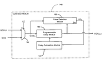
- the buffer control module 140 of the present disclosure includes a calibration module 148 .
- the calibration module 148 communicates with the clock distribution module 146 and the buffer 104 .
- the calibration module 148 receives the BCCLK from the clock distribution module 146 and a DQS signal from the buffer 104 .
- the calibration module 148 calculates a DQS delay value based on the BCCLK or another clock signal and delays the DQS signal based on the DQS delay value.
- the calibration module 148 uses the BCCLK to calculate the DQS delay value during DQS calibration cycles.
- DQS calibration cycles may coincide with idle periods of the buffer 104 .
- the calibration module 148 outputs a delayed DQS based on the DQS delay value.
- the buffer control module 140 uses the DQS delay signal as a clock signal to meet the timing requirements between the DQS signal and data.
- the DQS delay signal serves as a data sampling delay with respect to the read and/or write commands to the buffer 104 .
- the calibration module 148 delays the DQS signal by 1 ⁇ 4 of a frequency (i.e. 1 ⁇ 2 of a high clock width of the DQS signal) of the DQS signal.
- the calibration module 148 may be implemented by an existing integrated circuit and/or by additional integrated circuits. Alternatively, the calibration module 148 may be implemented as a SOC.
- the host 116 sends read and write commands to the HDC module 108 .
- the HDC module 108 stores the read and write commands in the buffer 104 .
- the processor 106 receives the read and write commands from the buffer 104 and executes firmware to control the HDC module 108 accordingly.
- the HDC module 108 reads data corresponding to the read commands from the HDDA 120 .
- the buffer control module 140 and the ECC module 142 receive the data from the HDDA 120 .
- the ECC module 142 provides an ECC mask for errors that may have occurred during read operations while the data is still in the buffer control module 140 . After any errors in the data are corrected, the data is transferred to the buffer 104 . The data is then transferred from the buffer 104 to the host 116 .
- the disk formatter module 144 controls writing of data to the HDDA 120 .
- the buffer 104 receives data corresponding to the write commands via the HDC module 108 .
- the disk formatter module 144 receives the data from the buffer 104 via the HDC module 108 .
- the disk formatter module 144 formats the data for writing to the HDDA 120 .
- the disk formatter module 144 adds error correction codes to the data, monitors a position of the read/write heads, and writes the data to the read/write heads as described in FIG. 1 .
- the clock distribution module 146 communicates with the buffer control module 140 and the oscillator 105 .
- the clock distribution module 146 includes a phase locked loop (PLL) module 160 , a voltage regulator (VCO) module 162 , and a clock distribution logic (CDL) module 164 .
- the PLL module 160 controls the oscillator 105 in order to maintain a constant phase angle (i.e. lock) on a frequency of an input or reference signal.
- the PLL module 160 communicates with the VCO module 162 and the CDL module 164 .
- the CDL module 164 generates and outputs the BCCLK.
- the calibration module 148 receives the DQS signal and data from the buffer 104 .
- the calibration module 148 includes a logic module 182 (such as a multiplexer), a programmable delay module 184 , a pulse detection module 186 , and a delay calculation module 187 .
- the calibration module 148 determines the DQS delay value during a calibration cycle.
- the programmable delay module 184 applies the DQS delay value to the DQS signal.
- the calibration module 148 delays the DQS signal based on the DQS delay value that is based on one of a calculated delay value or a state machine delay value.
- the calibration module 148 determines an optimal delay that is compatible with worst-case (e.g. 3 nanoseconds) and best-case (e.g. 1.5 nanoseconds) delay conditions by dynamically adjusting the DQS delay value.
- the dynamic adjustment allows for increased transfer rates to and/or from the buffer 104 .
- the logic module 182 receives the DQS and the BCCLK, as well as a calibration cycle (CC) select signal.
- the CC select signal selects the DQS and the logic module 182 outputs a DQS input signal (DQS IN ) accordingly.
- the programmable delay module 184 delays DQS IN based on the programmable delay value and outputs a delayed DQS output signal (DQS OUT ).
- the CC select signal selects the BCCLK and the logic module 182 outputs DQS IN based on the BCCLK.
- the buffer 104 does not generate the DQS and the calibration module 148 calibrates the programmable delay based on the BCCLK.
- the programmable delay module 184 delays DQS IN and outputs DQS OUT .
- the pulse detection module 186 receives and compares phases of DQS IN and DQS OUT and outputs a pulse detection signal PD C based on a delay between DQS IN and DQS OUT .
- the delay calculation module 187 receives the pulse detection signal PD C and can program the programmable delay module 187 with a calculated delay value based on PD C . In other words, the delay calculation module 187 can calculate the DQS delay based on feedback from the pulse detection module 186 .
- the delay calculation module 187 includes a logic module 188 (such as a multiplexer), a state machine module 190 , a counter module 192 , a register module 194 , and a calculator module 196 .
- a register module 180 receives and stores the data.
- the programmable delay module 184 delays DQS IN based on the DQS delay value received from the logic module 188 .
- the logic module 188 outputs the DQS delay value based on one of a calculated delay value C D received from the calculator module 196 and a state machine delay value received from the state machine module 190 .
- the logic module 188 selectively outputs one of the calculated delay value C D and the state machine delay value based on a control signal SM A received from the state machine module 190 .
- the state machine module 190 may override the calculated delay value C D with the state machine delay value.
- the state machine module 190 determines the delay of the DQS signal.
- the state machine module 190 cycles through a plurality of delay values (e.g. 0 to 31) during each calibration cycle. The calibration cycle is complete after the calibration module 148 tests the maximum delay value of the plurality of delay values.
- the calibration module 148 executes calibration cycles to compensate for process, voltage, and/or temperature variations of the HDD system 100 .
- the state machine module 190 transmits an enable signal EN to the pulse detection module 186 .
- the pulse detection module 186 receives and compares phases of DQS IN and DQS OUT . More specifically, the pulse detection module 186 determines the delay of DQS OUT with respect to DQS IN . The pulse detection module 186 determines whether the delay is above or below a threshold value. The threshold value represents a desired delay of the DQS (e.g. one-half clock period). For example, the pulse detection module 186 generates the pulse detection signal PD C when there is an overlap between pulses of DQS IN and DQS OUT (i.e. the delay is less than one-half clock period). When there is no overlap between the pulses (i.e. the delay is approximately one-half clock period), the pulse detection module 186 does not generate the pulse detection signal PD C .
- the threshold value represents a desired delay of the DQS (e.g. one-half clock period).
- the pulse detection module 186 generates the pulse detection signal PD C when there is an overlap between pulses of DQS IN and DQS OUT
- the pulse detection module 186 transmits the pulse detection signal PD C to the counter module 192 .
- the counter module 192 increments a count value based on the pulse detection signal PD C . For example, the counter module 192 increments the count value when the counter module 192 receives a stream of the pulse detection signal PD C during a particular calibration cycle. Conversely, the counter module 192 does not increment the count value when the pulse detection signal PD C is not generated by the pulse detection module 186 during a calibration cycle.
- the state machine module 190 may reset the operation of the calibration module 148 by transmitting a reset signal (SM R ) to the counter module 192 .
- SM R reset signal
- the register module 194 stores the count value received from the counter module 192 and transmits the count value to the calculator module 196 .
- the register module 194 may also store delay values calculated in a particular calibration cycle for future use by the calibration module 148 during subsequent calibrations.
- the calculator module 196 calculates the calculated delay value C D by dividing the count value by a divide value (e.g. 2).
- the calculator module 196 can add or subtract a bias value (e.g. 1 or 2) to the calculated delay value C D to compensate for nonlinearities of the calculated delay value C D based on inequalities in wiring delays.
- a timing diagram illustrates a calibrated DQS signal 200 centered within a valid data window 202 .
- the DQS signal 200 controls the sampling of data from the buffer 104 . Centering the data read operation within the DQS signal window 202 allows for improved data transfer rates to and/or from the buffer 104 and prevents false readings.
- the method 300 begins at step 302 .
- the state machine module 190 enters a calibration cycle after counter module 192 is cleared from a previous calibration cycle.
- the state machine module 190 transmits a state machine delay value to the programmable delay module 184 .
- the state machine module 190 enables the pulse detection module 186 .
- the pulse detection module 186 compares the DQS OUT with a threshold value.
- the counter module 192 increments a count value based on a pulse detection signal PD C generated by the pulse detection module 186 .
- step 314 the calibration module 148 determines whether the calibration cycle is complete. If the calibration cycle is not complete, the calibration module 148 proceeds to step 316 . In step 316 , the state machine module 190 increments the state machine delay and returns to step 306 . If the calibration cycle is complete, the calibration module 148 proceeds to step 318 .
- step 318 the calculator module 196 calculates a calculated delay value C D based on the count value.
- step 320 the programmable delay module 184 generates DQS OUT based on the calculated delay value C D .
- the method 300 ends in step 318 .
- the calibration system can be implemented in a digital versatile disc (DVD) drive 410 .
- the DVD drive 410 includes either or both signal processing and/or control circuit, which are generally identified in FIG. 7A at 412 , mass data storage 418 and/or a power supply 413 .
- the mass data storage 418 may implement the calibration system.
- the signal processing and/or control circuit 412 and/or other circuits (not shown) in the DVD drive 410 may process data, perform coding and/or encryption, perform calculations, and/or format data that is read from and/or data written to an optical storage medium 416 .
- the signal processing and/or control circuit 412 and/or other circuits (not shown) in the DVD drive 410 can also perform other functions such as encoding and/or decoding and/or any other signal processing functions associated with a DVD drive.
- the DVD drive 410 may communicate with an output device (not shown) such as a computer, television or other device via one or more wired or wireless communication links 417 .
- the DVD drive 410 may communicate with mass data storage 418 that stores data in a nonvolatile manner.
- the mass data storage 418 may include a hard disk drive (HDD).
- the HDD may have the configuration shown in FIG. 1 .
- the HDD may be a mini HDD that includes one or more platters having a diameter that is smaller than approximately 1.8′′.
- the DVD drive 410 may be connected to memory 419 such as RAM, ROM, low latency nonvolatile memory such as flash memory and/or other suitable electronic data storage.
- the calibration system can be implemented in a high definition television (HDTV) 420 .
- the HDTV 420 includes either or both signal processing and/or control circuit, which are generally identified in FIG. 7B at 422 , a WLAN interface 429 , mass data storage 627 , and/or a power supply 423 .
- the mass data storage 427 may implement the calibration system.
- the mass data storage 427 may include one or more buffer memories that temporarily store data that is transmitted to and from the HDTV 420 .
- the memory controller module that manages the buffer memories may implement the calibration system.
- the HDTV 420 receives HDTV input signals in either a wired or wireless format and generates HDTV output signals for a display 426 .
- signal processing circuit and/or control circuit 422 and/or other circuits (not shown) of the HDTV 420 may process data, perform coding and/or encryption, perform calculations, format data and/or perform any other type of HDTV processing that may be required.
- the HDTV 420 may communicate with mass data storage 427 that stores data in a nonvolatile manner such as optical and/or magnetic storage devices including, but not limited to, DVD drives and HDDs. At least one HDD may have the configuration shown in FIG. 1 and/or at least one DVD drive may have the configuration shown in FIG. 7A .
- the HDD may be a mini HDD that includes one or more platters having a diameter that is smaller than approximately 1.8′′.
- the HDTV 420 may be connected to memory 428 such as RAM, ROM, low latency nonvolatile memory such as flash memory and/or other suitable electronic data storage.
- the HDTV 420 also may support connections with the WLAN via the WLAN interface 429 .
- the vehicle 430 includes a powertrain control system 432 , a WLAN interface 448 , mass data storage 446 and/or a power supply 433 .
- the mass data storage 446 may implement the calibration system.
- the mass data storage 446 may include one or more buffer memories that temporarily store data that is transmitted to and from the powertrain control system 432 .
- the memory controller module that manages the buffer memories may implement the calibration system.
- the powertrain control system 432 receives inputs from one or more sensors 436 such as temperature sensors, pressure sensors, rotational sensors, airflow sensors and/or any other suitable sensors and/or that generates one or more output control signals 438 such as engine operating parameters, transmission operating parameters, and/or other control signals.
- the calibration system may also be implemented in an other vehicle control system 440 of the vehicle 430 .
- the control system 440 may likewise receive signals from input sensors 442 and/or output control signals to one or more output devices 444 .
- the control system 440 may be part of an anti-lock braking system (ABS), a navigation system, a telematics system, a vehicle telematics system, a lane departure system, an adaptive cruise control system, a vehicle entertainment system such as a stereo, DVD, compact disc system and the like. Still other implementations are contemplated.
- ABS anti-lock braking system
- the powertrain control system 432 may communicate with mass data storage 446 that stores data in a nonvolatile manner.
- the mass data storage 446 may include optical and/or magnetic storage devices such as hard disk drives (HDDs) and/or DVD drives. At least one HDD may have the configuration shown in FIG. 1 and/or at least one DVD drive may have the configuration shown in FIG. 7A .
- the HDD may be a mini HDD that includes one or more platters having a diameter that is smaller than approximately 1.8′′.
- the powertrain control system 432 may be connected to memory 447 such as RAM, ROM, low latency nonvolatile memory such as flash memory and/or other suitable electronic data storage.
- the powertrain control system 432 also may support connections with a WLAN via the WLAN interface 448 .
- the control system 440 may also include mass data storage, memory and/or a WLAN interface (all not shown).
- the calibration system can be implemented in a cellular phone 450 that may include a cellular antenna 451 .
- the cellular phone 450 includes either or both signal processing and/or control circuit, which are generally identified in FIG. 7D at 452 , a WLAN interface 468 , mass data storage 464 and/or a power supply 453 .
- the mass data storage 464 of the cellular phone 450 may implement the calibration system.
- the mass data storage 464 may include one or more buffer memories that temporarily store data that is transmitted to and from the cellular phone 450 .
- the memory controller module that manages the buffer memories may implement the calibration system.
- the cellular phone 450 includes a microphone 456 , an audio output 458 such as a speaker and/or audio output jack, a display 460 and/or an input device 462 such as a keypad, pointing device, voice actuation and/or other input device.
- the signal processing and/or control circuit 452 and/or other circuits (not shown) in the cellular phone 450 may process data, perform coding and/or encryption, perform calculations, format data and/or perform other cellular phone functions.
- the cellular phone 450 may communicate with mass data storage 464 that stores data in a nonvolatile manner such as optical and/or magnetic storage devices including hard disk drives (HDDs) and/or DVD drives. At least one HDD may have the configuration shown in FIG. 1 and/or at least one DVD drive may have the configuration shown in FIG. 7A .
- the HDD may be a mini HDD that includes one or more platters having a diameter that is smaller than approximately 1.8′′.
- the cellular phone 450 may be connected to memory 466 such as RAM, ROM, low latency nonvolatile memory such as flash memory and/or other suitable electronic data storage.
- the cellular phone 450 also may support connections with a WLAN via the WLAN interface 468 .
- the calibration system can be implemented in a set top box 480 .
- the set top box 480 includes either or both signal processing and/or control circuit, which are generally identified in FIG. 7E at 484 , a WLAN interface 496 , mass data storage 490 and/or a power supply 483 .
- the mass data storage 490 of the set top box 480 may implement the calibration system.
- the mass data storage 490 may include one or more buffer memories that temporarily store data that is transmitted to and from the set top box 480 .
- the memory controller module that manages the buffer memories may implement the calibration system.
- the set top box 480 receives signals from a source such as a broadband source and outputs standard and/or high definition audio/video signals suitable for a display 488 such as a television, a monitor and/or other video and/or audio output devices.
- the signal processing and/or control circuit 484 and/or other circuits (not shown) of the set top box 480 may process data, perform coding and/or encryption, perform calculations, format data and/or perform any other set top box function.
- the set top box 480 may communicate with mass data storage 490 that stores data in a nonvolatile manner.
- the mass data storage 490 may include optical and/or magnetic storage devices such as hard disk drives (HDDs) and/or DVD drives. At least one HDD may have the configuration shown in FIG. 1 and/or at least one DVD drive may have the configuration shown in FIG. 7A .
- the HDD may be a mini HDD that includes one or more platters having a diameter that is smaller than approximately 1.8′′.
- the set top box 480 may be connected to memory 494 such as RAM, ROM, low latency nonvolatile memory such as flash memory and/or other suitable electronic data storage.
- the set top box 480 also may support connections with a WLAN via the WLAN interface 496 .
- the calibration system can be implemented in a media player 500 .
- the media player 500 includes either or both signal processing and/or control circuit, which are generally identified in FIG. 7F at 504 , a WLAN interface 516 , mass data storage 510 and/or a power supply 513 .
- the mass data storage 510 of the media player 500 may implement the calibration system.
- the mass data storage 510 may include one or more buffer memories that temporarily store data that is transmitted to and from the media player 500 .
- the memory controller module that manages the buffer memories may implement the calibration system.
- the media player 500 includes a display 507 and/or a user input 508 such as a keypad, touchpad and the like.
- the media player 500 may employ a graphical user interface (GUI) that typically employs menus, drop down menus, icons and/or a point-and-click interface via the display 507 and/or user input 508 .
- GUI graphical user interface
- the media player 500 further includes an audio output 509 such as a speaker and/or audio output jack.
- the signal processing and/or control circuit 504 and/or other circuits (not shown) of the media player 500 may process data, perform coding and/or encryption, perform calculations, format data and/or perform any other media player function.
- the media player 500 may communicate with mass data storage 510 that stores data such as compressed audio and/or video content in a nonvolatile manner.
- the compressed audio files include files that are compliant with MP3 format or other suitable compressed audio and/or video formats.
- the mass data storage 510 may include optical and/or magnetic storage devices such as hard disk drives (HDDs) and/or DVD drives. At least one HDD may have the configuration shown in FIG. 1 and/or at least one DVD drive may have the configuration shown in FIG. 7A .
- the HDD may be a mini HDD that includes one or more platters having a diameter that is smaller than approximately 1.8′′.
- the media player 500 may be connected to memory 514 such as RAM, ROM, low latency nonvolatile memory such as flash memory and/or other suitable electronic data storage.
- the media player 500 also may support connections with a WLAN via the WLAN interface 516 . Still other implementations in addition to those described above are contemplated.
Abstract
Description
Claims (37)
Priority Applications (2)
| Application Number | Priority Date | Filing Date | Title |
|---|---|---|---|
| US11/526,398 US7793063B1 (en) | 2005-09-29 | 2006-09-25 | Method and system for automatic calibration of a DQS signal in a storage controller |
| US12/874,349 US8019957B1 (en) | 2005-09-29 | 2010-09-02 | Method and system for automatic calibration of a DQS signal in a storage controller |
Applications Claiming Priority (2)
| Application Number | Priority Date | Filing Date | Title |
|---|---|---|---|
| US72169005P | 2005-09-29 | 2005-09-29 | |
| US11/526,398 US7793063B1 (en) | 2005-09-29 | 2006-09-25 | Method and system for automatic calibration of a DQS signal in a storage controller |
Related Child Applications (1)
| Application Number | Title | Priority Date | Filing Date |
|---|---|---|---|
| US12/874,349 Continuation US8019957B1 (en) | 2005-09-29 | 2010-09-02 | Method and system for automatic calibration of a DQS signal in a storage controller |
Publications (1)
| Publication Number | Publication Date |
|---|---|
| US7793063B1 true US7793063B1 (en) | 2010-09-07 |
Family
ID=42669765
Family Applications (2)
| Application Number | Title | Priority Date | Filing Date |
|---|---|---|---|
| US11/526,398 Active 2028-03-31 US7793063B1 (en) | 2005-09-29 | 2006-09-25 | Method and system for automatic calibration of a DQS signal in a storage controller |
| US12/874,349 Active US8019957B1 (en) | 2005-09-29 | 2010-09-02 | Method and system for automatic calibration of a DQS signal in a storage controller |
Family Applications After (1)
| Application Number | Title | Priority Date | Filing Date |
|---|---|---|---|
| US12/874,349 Active US8019957B1 (en) | 2005-09-29 | 2010-09-02 | Method and system for automatic calibration of a DQS signal in a storage controller |
Country Status (1)
| Country | Link |
|---|---|
| US (2) | US7793063B1 (en) |
Cited By (5)
| Publication number | Priority date | Publication date | Assignee | Title |
|---|---|---|---|---|
| US8046185B1 (en) * | 2007-05-30 | 2011-10-25 | Marvell International Ltd. | Oscillator calibration for motor controller |
| US8681575B2 (en) | 2011-03-24 | 2014-03-25 | Kabushiki Kaisha Toshiba | Semiconductor device |
| US20160077759A1 (en) * | 2014-09-16 | 2016-03-17 | Mediatek Inc. | Memory-access method using batch command queue and associated controller |
| US9466349B1 (en) * | 2015-06-15 | 2016-10-11 | SK Hynix Inc. | Semiconductor system with training function for a data strobe signal |
| US11481124B2 (en) * | 2019-12-03 | 2022-10-25 | SK Hynix Inc. | Memory systems and methods of training the memory systems |
Families Citing this family (12)
| Publication number | Priority date | Publication date | Assignee | Title |
|---|---|---|---|---|
| US7543172B2 (en) | 2004-12-21 | 2009-06-02 | Rambus Inc. | Strobe masking in a signaling system having multiple clock domains |
| US8272781B2 (en) * | 2006-08-01 | 2012-09-25 | Intel Corporation | Dynamic power control of a memory device thermal sensor |
| US8307270B2 (en) * | 2009-09-03 | 2012-11-06 | International Business Machines Corporation | Advanced memory device having improved performance, reduced power and increased reliability |
| US9607714B2 (en) | 2012-12-26 | 2017-03-28 | Nvidia Corporation | Hardware command training for memory using write leveling mechanism |
| US9824772B2 (en) | 2012-12-26 | 2017-11-21 | Nvidia Corporation | Hardware chip select training for memory using read commands |
| US20140181429A1 (en) * | 2012-12-26 | 2014-06-26 | Nvidia Corporation | Multi-dimensional hardware data training between memory controller and memory |
| US9378169B2 (en) | 2012-12-31 | 2016-06-28 | Nvidia Corporation | Method and system for changing bus direction in memory systems |
| KR102197943B1 (en) | 2014-04-04 | 2021-01-05 | 삼성전자주식회사 | Memory controller and systme including the same |
| US9413344B2 (en) | 2014-09-08 | 2016-08-09 | Qualcomm Incorporated | Automatic calibration circuits for operational calibration of critical-path time delays in adaptive clock distribution systems, and related methods and systems |
| CN110648703B (en) * | 2018-06-26 | 2021-06-15 | 龙芯中科技术股份有限公司 | Data acquisition circuit, and method and device for controlling read data window |
| US11609868B1 (en) * | 2020-12-31 | 2023-03-21 | Waymo Llc | Control calibration timing to avoid memory write blackout period |
| CN115865755B (en) * | 2022-11-18 | 2024-03-22 | 电子科技大学 | Parallel data calibration method for interconnection among multiple networks and electronic equipment |
Citations (5)
| Publication number | Priority date | Publication date | Assignee | Title |
|---|---|---|---|---|
| US20020184461A1 (en) * | 2001-05-31 | 2002-12-05 | Zumkehr John F. | Method and apparatus for control calibration of multiple memory modules within a memory channel |
| US6760856B1 (en) * | 2000-07-17 | 2004-07-06 | International Business Machines Corporation | Programmable compensated delay for DDR SDRAM interface using programmable delay loop for reference calibration |
| US20060052961A1 (en) * | 2004-08-20 | 2006-03-09 | Best Scott C | Individual data line strobe-offset control in memory systems |
| US7412616B2 (en) * | 2003-09-03 | 2008-08-12 | Renesas Technology Corp. | Semiconductor integrated circuit |
| US7512193B1 (en) * | 2005-05-02 | 2009-03-31 | National Semiconductor Corporation | Circuit and method for pre-emphasis in data serialization |
-
2006
- 2006-09-25 US US11/526,398 patent/US7793063B1/en active Active
-
2010
- 2010-09-02 US US12/874,349 patent/US8019957B1/en active Active
Patent Citations (5)
| Publication number | Priority date | Publication date | Assignee | Title |
|---|---|---|---|---|
| US6760856B1 (en) * | 2000-07-17 | 2004-07-06 | International Business Machines Corporation | Programmable compensated delay for DDR SDRAM interface using programmable delay loop for reference calibration |
| US20020184461A1 (en) * | 2001-05-31 | 2002-12-05 | Zumkehr John F. | Method and apparatus for control calibration of multiple memory modules within a memory channel |
| US7412616B2 (en) * | 2003-09-03 | 2008-08-12 | Renesas Technology Corp. | Semiconductor integrated circuit |
| US20060052961A1 (en) * | 2004-08-20 | 2006-03-09 | Best Scott C | Individual data line strobe-offset control in memory systems |
| US7512193B1 (en) * | 2005-05-02 | 2009-03-31 | National Semiconductor Corporation | Circuit and method for pre-emphasis in data serialization |
Cited By (6)
| Publication number | Priority date | Publication date | Assignee | Title |
|---|---|---|---|---|
| US8046185B1 (en) * | 2007-05-30 | 2011-10-25 | Marvell International Ltd. | Oscillator calibration for motor controller |
| US8681575B2 (en) | 2011-03-24 | 2014-03-25 | Kabushiki Kaisha Toshiba | Semiconductor device |
| US20160077759A1 (en) * | 2014-09-16 | 2016-03-17 | Mediatek Inc. | Memory-access method using batch command queue and associated controller |
| US9886207B2 (en) * | 2014-09-16 | 2018-02-06 | Mediatek Inc. | Memory-access method using batch command queue and associated controller |
| US9466349B1 (en) * | 2015-06-15 | 2016-10-11 | SK Hynix Inc. | Semiconductor system with training function for a data strobe signal |
| US11481124B2 (en) * | 2019-12-03 | 2022-10-25 | SK Hynix Inc. | Memory systems and methods of training the memory systems |
Also Published As
| Publication number | Publication date |
|---|---|
| US8019957B1 (en) | 2011-09-13 |
Similar Documents
| Publication | Publication Date | Title |
|---|---|---|
| US7793063B1 (en) | Method and system for automatic calibration of a DQS signal in a storage controller | |
| US7865784B1 (en) | Write validation | |
| US7411758B1 (en) | Disk drive servo control using spirals | |
| US8935591B1 (en) | System and method to correct errors in data read from a source supplying streaming data | |
| US7978541B2 (en) | High speed interface for multi-level memory | |
| US7733588B1 (en) | Repetitive feed-forward algorithm for self-servo-write PLL | |
| US7921243B1 (en) | System and method for a DDR SDRAM controller | |
| CN113557569B (en) | Constant density writing for magnetic storage media | |
| US8090932B1 (en) | Communication bus with hidden pre-fetch registers | |
| US8046185B1 (en) | Oscillator calibration for motor controller | |
| US9343103B2 (en) | Serial port communication for storage device using single bidirectional serial data line | |
| US7945812B1 (en) | System and method for error correction | |
| US7949838B1 (en) | System and method for managing a memory storage device | |
| US8077419B1 (en) | Method and apparatus for adjusting a gain of a variable gain amplifier in a read channel module | |
| US8023217B1 (en) | Method and system for read gate timing control for storage controllers | |
| CN101620880B (en) | Memory controller, PCB, computer system and memory adjusting method | |
| US20100153801A1 (en) | Method for at speed testing of devices | |
| US8046541B1 (en) | System for calibrating memory | |
| US8031424B2 (en) | Method and apparatus for testing electronics of a storage system | |
| US11652583B2 (en) | Electronic communication device, magnetic disk device and serial communication method | |
| US20180012627A1 (en) | Managing far and near track erasure by dynamic control of a write current parameter of a magnetic disk drive | |
| JP2007317263A (en) | Serial data transfer method and system thereof, and data storage device | |
| US8019936B1 (en) | Fast disk start system | |
| US9064539B1 (en) | Systems and methods for timing control in a data processing system | |
| US20110188147A1 (en) | Method adjusting gain of variable gain amplifier and apparatus using same |
Legal Events
| Date | Code | Title | Description |
|---|---|---|---|
| AS | Assignment |
Owner name: MARVELL INTERNATIONAL LTD., BERMUDA Free format text: ASSIGNMENT OF ASSIGNORS INTEREST;ASSIGNOR:MARVELL SEMICONDUCTOR, INC.;REEL/FRAME:018343/0767 Effective date: 20060925 Owner name: MARVELL SEMICONDUCTOR, INC., CALIFORNIA Free format text: ASSIGNMENT OF ASSIGNORS INTEREST;ASSIGNORS:WHITE, THEODORE C.;LE, THANH H.;REEL/FRAME:018343/0763 Effective date: 20060922 |
|
| STCF | Information on status: patent grant |
Free format text: PATENTED CASE |
|
| FPAY | Fee payment |
Year of fee payment: 4 |
|
| MAFP | Maintenance fee payment |
Free format text: PAYMENT OF MAINTENANCE FEE, 8TH YEAR, LARGE ENTITY (ORIGINAL EVENT CODE: M1552) Year of fee payment: 8 |
|
| AS | Assignment |
Owner name: CAVIUM INTERNATIONAL, CAYMAN ISLANDS Free format text: ASSIGNMENT OF ASSIGNORS INTEREST;ASSIGNOR:MARVELL INTERNATIONAL LTD.;REEL/FRAME:052918/0001 Effective date: 20191231 |
|
| AS | Assignment |
Owner name: MARVELL ASIA PTE, LTD., SINGAPORE Free format text: ASSIGNMENT OF ASSIGNORS INTEREST;ASSIGNOR:CAVIUM INTERNATIONAL;REEL/FRAME:053475/0001 Effective date: 20191231 |
|
| MAFP | Maintenance fee payment |
Free format text: PAYMENT OF MAINTENANCE FEE, 12TH YEAR, LARGE ENTITY (ORIGINAL EVENT CODE: M1553); ENTITY STATUS OF PATENT OWNER: LARGE ENTITY Year of fee payment: 12 |