US7790600B2 - Synthesis of zeolite crystals and formation of carbon nanostructures in patterned structures - Google Patents
Synthesis of zeolite crystals and formation of carbon nanostructures in patterned structures Download PDFInfo
- Publication number
- US7790600B2 US7790600B2 US12/358,063 US35806309A US7790600B2 US 7790600 B2 US7790600 B2 US 7790600B2 US 35806309 A US35806309 A US 35806309A US 7790600 B2 US7790600 B2 US 7790600B2
- Authority
- US
- United States
- Prior art keywords
- zeolite
- zeolite crystals
- patterned structures
- substrate
- carbon nanostructures
- Prior art date
- Legal status (The legal status is an assumption and is not a legal conclusion. Google has not performed a legal analysis and makes no representation as to the accuracy of the status listed.)
- Expired - Fee Related, expires
Links
Images


Classifications
-
- B—PERFORMING OPERATIONS; TRANSPORTING
- B82—NANOTECHNOLOGY
- B82Y—SPECIFIC USES OR APPLICATIONS OF NANOSTRUCTURES; MEASUREMENT OR ANALYSIS OF NANOSTRUCTURES; MANUFACTURE OR TREATMENT OF NANOSTRUCTURES
- B82Y40/00—Manufacture or treatment of nanostructures
-
- C—CHEMISTRY; METALLURGY
- C01—INORGANIC CHEMISTRY
- C01B—NON-METALLIC ELEMENTS; COMPOUNDS THEREOF; METALLOIDS OR COMPOUNDS THEREOF NOT COVERED BY SUBCLASS C01C
- C01B32/00—Carbon; Compounds thereof
- C01B32/15—Nano-sized carbon materials
- C01B32/158—Carbon nanotubes
- C01B32/16—Preparation
-
- B—PERFORMING OPERATIONS; TRANSPORTING
- B82—NANOTECHNOLOGY
- B82Y—SPECIFIC USES OR APPLICATIONS OF NANOSTRUCTURES; MEASUREMENT OR ANALYSIS OF NANOSTRUCTURES; MANUFACTURE OR TREATMENT OF NANOSTRUCTURES
- B82Y30/00—Nanotechnology for materials or surface science, e.g. nanocomposites
Definitions
- Patterned structures comprising zeolite crystals and a method for the synthesis of these zeolite crystals in the patterned structures are provided, as is a method to form carbon nanostructures such as carbon nanotubes (CNT) in high yields inside the zeolite crystals.
- a method is provided to synthesize carbon nanostructures within the parallel pores of a zeolite crystal thereby making use of an organo-metal complex introduced via impregnation or in situ synthesis so ensuring 100% pore filling and high efficiency for synthesis of resulting carbon nanostructures; the metal being useful to initiate the growth of the carbon nanostructures.
- the methods and structures are useful in the field of semiconductor processing and the use of carbon nanostructures in zeolite crystals within patterned structures such as trenches and/or vias as interconnect structures in a semiconductor device.
- Hybrid systems of interconnect structures are provided wherein both copper and carbon nanostructures are used as conductive material within vias and trenches.
- the methods and structures are also useful in the field of wafer stacking (3D applications), sensor applications (CNT acting as micro-electrode array), heat dissipation and fuel cells.
- a method is provided for integrating zeolite crystals in patterned structures (e.g.
- zeolite crystals for the synthesis of carbon nanostructures such that the carbon nanostructures can be used as interconnects in a semiconductor device, as is to a method for integrating zeolite crystals in patterned structures in a semiconductor device.
- Carbon Nanotubes are good candidates to replace copper for use as interconnect lines (trenches) and vias in future semiconductor devices. It is shown that for relevant interconnect lengths the resistance of the optimal CNT interconnect is about an order of magnitude smaller than the resistance of a copper interconnect. When fully ballistic transport can be achieved in the carbon nanotubes, the improvement in resistance is larger, up to several orders of magnitude.
- SW-CNT metallic single-walled carbon nanotubes
- Carbon nanostructures have been made in prior art by the template technique, using porous Alumina Oxide (AAO) as reported by Kyotani et al. (Chemistry of Materials, 8, 2109-2113, 1996), using mesoporous materials such as MCM-41 as reported by Urban et al. (Chemical Physics Letters, 359, 95-100, 2002) or using an AFI type zeolite as reported by Tang et al. (Applied Physics Letters, 73, 2287-2289, 1998).
- AAO porous Alumina Oxide
- zeolites Since zeolites have high pore densities in agreement with the strict requirements for CNT, they are very good candidates to produce highly dense aligned and isolated CNT within these pores. However to really exploit the interesting properties of zeolites for carbon nanostructure growth in patterned structures such as trenches and vias, zeolite growth must be integrated in the CMOS technology platform.
- a method is provided to incorporate zeolite crystals in patterned structures.
- the zeolite crystals having pores (channels) with an orientation which is defined by the topology of the zeolite crystal type and the geometry of the patterned structure resulting in pores parallel with the length axis of the patterned structures.
- Said patterned structures may be vias (vertical contacts) and trenches (horizontal lines) in a semiconductor substrate.
- the growth of CNT is achieved within the porous structure of the zeolite crystals whereby the pores can be defined as confined spaces (channels) in nanometer dimensions acting as a micro-reactor for CNT growth.
- the improved growth method gives a significantly higher carbon density (yield) compared to state of the art techniques.
- New zeolite topologies and nanocarbon synthesis techniques are provided resulting in significantly improved yields of intraporous carbon nanostructure growth.
- the methods of preferred embodiments offer advantages over state of the art techniques to position zeolite crystals in patterned structures.
- the methods of preferred embodiments accomplish this by first substantially filling the patterned structures with the zeolite synthesis solution or gel using mechanical forces before the crystallization of the synthesis gel to form zeolite crystals.
- VLS Vapor Liquid Solid
- the methods of preferred embodiments have the advantage that the predetermined size and geometry of the pores within the pores of the zeolite can be used to determine the diameter and hence properties of the synthesized carbon nanostructures (e.g. SW-CNT versus MW-CNT).
- the methods of preferred embodiments for providing carbon nanostructures within patterned structures further have the advantage over state of the art techniques to grow easily carbon nanostructures in horizontal direction e.g. along the length of a trench.
- Using methods of the preferred embodiments it is possible to direct the zeolite crystal growth (and hence orient the pores within the structure of the zeolite) in a direction defined by the confinement of the structures. In other words it may be defined by the geometric parameters (depth versus length) of the patterned structure. In this way it is possible to achieve direct vertical growth of the zeolite crystal in a via (vertical hole), direct horizontal growth of the zeolite crystal in a trench (horizontal line). Hence it is possible to induce vertical or horizontal growth of carbon nanostructures inside zeolite pores.
- a substrate comprising patterned structures (openings) wherein these patterned structures are filled with zeolite crystals wherein the zeolite crystals and hence pores within the zeolite have an orientation in the direction defined by the confinement of the patterned structures.
- a method for providing zeolite crystals within patterned structures comprises at least the steps of: providing a substrate comprising in its top surface patterned structures (openings), impregnating a zeolite synthesis solution or gel onto the substrate followed by, applying mechanical forces to incorporate the synthesis solution into the patterned structures, applying hydrothermal conditions to crystallize the zeolite synthesis solution to form zeolite crystals, rinsing and drying the substrate, and optionally applying additional mechanical forces to remove non-incorporated or non-attached zeolite crystals.
- the method to incorporate zeolite crystals within patterned structures is used for dense and aligned growth of carbon nanostructures (e.g. CNT) within the pores of the zeolite structure.
- the method to grow carbon nanostructures within patterned structures using zeolite crystals comprises after the steps of providing the zeolite crystals within the patterned structures as described above at least the step of heating the zeolite crystals in the presence of an inert gas or a mixture of an inert gas and a carbon containing gas at a temperature between 350° C.-1000° C.
- the method for providing zeolite crystals in patterned structures and subsequently grow carbon nanostructures within the pores of the zeolite comprises at least the steps of: providing a substrate comprising on its top surface patterned structures (openings), impregnating a zeolite synthesis solution or gel onto the substrate followed by, applying mechanical forces to incorporate the synthesis solution into the patterned structures, applying hydrothermal conditions to crystallize the zeolite from the synthesis solution or gel, rinsing and drying the substrate, and optionally applying mechanical forces to remove non-incorporated or non-attached zeolite crystals, and heating the zeolite crystals in the presence of an inert gas or a mixture of an inert gas and a carbon containing gas at a temperature between 350° C.-1000° C. to grow the carbon nanostructures.
- an improved method is provided to grow carbon nanostructures (e.g. CNT) within the pores of a zeolite crystal.
- the improved method gives rise to significantly higher yields of intraporous nanocarbon growth compared to the prior art techniques.
- the highest achieved (reported) pore filling degree in prior art is 28% by addition of hydrocarbon gas during pyrolysis.
- pore filling degrees of 60% and more are achieved without addition of hydrocarbon gas during pyrolysis.
- the improved method makes use of organo-metal complexes which are incorporated into the pores of the zeolite crystals after the step of forming the zeolite crystal and which are used as initiator and carbon source for the subsequent step of carbon nanostructure growth.
- the organo-metal complex according to the preferred embodiments may be introduced in the zeolite crystal pores by impregnation or in-situ synthesis. Addition of organo-metal complexes to the zeolite synthesis solution or gel has been described in prior art by Balkus Jr. et al. However the organo-metal complex was always added before zeolite crystallization. Using the method according to the prior art, the concentration of the complexes in the zeolite synthesis gel or solution should be low to allow zeolite crystallization, resulting in inefficient loading with carbon nanostructures.
- the organo-metal complex of the preferred embodiments is preferably a (metallo)-phthalocyanine complex.
- Phthalocyanines may be incorporated in extra large pore zeolites such as VFI type zeolites and can be converted into carbon nanostructures under pyrolysis conditions.
- Suitable phthalocyanine complexes are Ni-, Fe-, Co-, or even H2-phthalocyanine complexes, for example Fe-phthalocyanine.
- the improved method to grow the carbon nanostructures (e.g. CNT) within the pores of a zeolite crystal comprises at least the steps of: providing a zeolite synthesis solution or gel followed by, applying hydrothermal conditions to crystallize the zeolite synthesis solution to form zeolite crystals, heating the zeolite crystals and evaporating or impregnating a solid source or precursor of phthalocyanine and a metal at a temperature between 0° C.-400° C.
- the phthalocyanine and the metal form a metal-phthalocyanine complex within the pores of the zeolite crystals, and growing carbon nanostructures using the metal-phthalocyanine complex as an initiator by heating at a temperature between 350-1000° C.
- the improved method to grow the carbon nanostructures (e.g. CNT) within the pores of a zeolite crystal is compatible with the method to grow zeolite crystals within patterned structures as described above. According to preferred embodiments, the improved method to grow the carbon nanostructures (e.g.
- the phthalocyanine and the metal are forming a metal-phthalocyanine complex within the pores of the zeolite crystals, and growing carbon nanostructures using the metallo-phthalocyanine complex as an initiator by heating at a temperature between 350-1000° C.
- the substrate may be any suitable substrate which is chosen in function of further applications.
- the substrate may be a semiconductor substrate such as a Si or Ge wafer.
- the patterned structures may be trenches or via holes which may be patterned in a dielectric layer having a k value lower than 5.
- suitable dielectric layers are silicon dioxide and other state of the art low-k materials such as Black Diamond (Applied Materials).
- the patterning of the structures may be achieved using a combination of photolithographic imaging and (anisotropic) dry etching.
- the trenches and vias have preferably a diameter in the range of 50 nm up to 300 nm. Trenches have an aspect ratio (length/depth) greater than 1 whereas vias have an aspect ratio (length/depth) smaller than 1.
- the patterned structure may be a single level mask structure with vias ranging from 50 nm up to 300 nm in diameter.
- the vias may land on a single common bottom electrode that can be made from a suite of different materials.
- An example of a suitable bottom contact electrode material is TiN.
- the zeolite synthesis solution or gel may comprise a silicon source and an alkali source of inorganic or organic nature, and optionally a template molecule and hetero-elements such as Al, Ga, Ti, Fe, Co, Ge, P, or a mixture thereof.
- the zeolite synthesis solution or gel may comprise an aluminum and phosphorus source, as well as a source of acidity, and a template molecule and optionally hetero-elements such as Si, Ga, Ti, Fe, Co, Ge, or a mixture thereof.
- SAPO-5 zeolite type material also referred to as AFI type
- aluminum-isopropoxide is used as an aluminum source
- phosphoric acid as a phosphorus source
- TPA tripropylamine
- Aerosil200 Degussa
- the synthesis gel is preferably a water-based solution; alcohols such as ethanol may be added to improve the wetability of the gel.
- An optimized synthesis gel for a silico-aluminophosphate may have the following composition: 1 Al2O3:0.99 P2O5:1.2 TPA:400 H2O:20 Ethanol:0.01 SiO2.
- the organo-metal complex used for impregnation or in-situ synthesis in the zeolite pores, may consist of a transition metal in comprising Fe, Ni or Co and any organic ligand that sterically can be accommodated in the zeolite pores.
- the zeolite can be a crystalline porous material with parallel pores, preferably with one of the following structure types, as defined by the International Zeolite Association: AFI, VFI type material.
- AFI International Zeolite Association
- VFI type material
- the mechanical forces used to incorporate the synthesis gel are selected from sonication, vibration and/or spin-coating.
- Sonication may be used to incorporate the synthesis gel into the patterned structures, suitable sonication condition are e.g. 15 minutes at 47 kHz.
- Spin-coating may be used to remove excess of synthesis gel from the substrate, suitable spin-coating condition are e.g. 15000 rpm for 10 seconds.
- the hydrothermal treatment is used to crystallize the synthesis gel and thereby forming (ordered) zeolite crystals.
- Suitable hydrothermal conditions comprise the heating of the substrate under autogeneous pressure for 2-48 h at 100-200° C., more preferably for 14-15 h at 150-180° C.
- the rinsing and drying is performed using doubly-distilled water.
- the additional mechanical forces needed to remove non-incorporated or non-attached zeolite crystals is performed using sonication. After the sonication, the substrate is preferably again thoroughly rinsed with doubly-distilled water.
- the step of growing the carbon nanostructures is such that vertical growth of carbon nanostructures is achieved in a via (vertical hole) and horizontal growth of carbon nanostructures is achieved in a trench (horizontal line).
- the step of growing the carbon nanostructures is achieved using high temperature pyrolysis conditions.
- the carbon source needed for the nanostructure synthesis may originate from the organic template molecule used for zeolite synthesis.
- a carbon containing gas may be added to the atmosphere under pyrolysis conditions (possibly in high pressure conditions).
- Yet another alternative is the formation of organo-metal complexes within the porous structure of the zeolite crystal (such as metal phthalocyanine complexes) leading to a stacking of these organo-metal complexes inside the zeolite pores.
- the pyrolysis step used to grow carbon nanostructures is performed within a thermal reactor e.g. a furnace.
- the reactor must be capable of heating the zeolite crystals to a temperature up to 1000° C.
- the thermal reactor preferably includes a chamber that can be maintained at vacuum or at a desired pressure, and further includes means for enabling a gas flow into the chamber.
- Preferred pyrolysis may be the heating of the zeolite crystals under a flow of inert gas. Then keep the zeolite crystals isothermal at 400-900° C. for 10-3600 min, more preferably at 550° C. for 50-150 min.
- FIG. 1A is a flow diagram illustrating the different processing steps to synthesize zeolite crystals within patterned structures according to preferred embodiments.
- FIG. 1B is a flow diagram illustrating the different processing steps to synthesize zeolite crystals within patterned structures and subsequent growth of carbon nanostructures within the pores of the zeolite crystals by heating the zeolite crystals in the presence of a carbon comprising gas according to preferred embodiments.
- FIG. 1C is a flow diagram illustrating the different steps to synthesize carbon nanostructures within the pores of zeolite crystals using organo-metal complexes according to preferred embodiments.
- FIG. 1D is a flow diagram illustrating the different processing steps to synthesize zeolite crystals within patterned structures and subsequent growth of carbon nanostructures within the pores of the zeolite crystals using organo-metal complexes according to preferred embodiments.
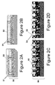
- FIGS. 2A and 2B illustrate a cross section of a substrate having patterned structures (openings) e.g. a BEST02 pattern with impregnated synthesis gel on top of the substrate.
- patterned structures e.g. a BEST02 pattern with impregnated synthesis gel on top of the substrate.
- FIG. 2C illustrates a cross section of the substrate having patterned structures after sonication (vibration) and hydrothermal treatment to obtain zeolite crystals inside the patterned structures.
- FIG. 2D illustrates a cross section of the substrate having patterned structures filled with zeolite crystals after performing pyrolysis to obtain carbon nanostructures inside the pores of the zeolite crystals.
- FIG. 3 illustrates a setup to perform the hydrothermal synthesis step according to preferred embodiments.
- FIG. 4 is a Scanning Electron Microscopy (SEM) image of AIPO-5 crystals which were grown in via holes on a BEST02 patterned wafer.
- FIG. 5A is a SEM image of the bottom side of a piece of zeolite crust grown on BEST02 patterned wafer and FIG. 5B illustrates a schematic view of the zeolite crust and related BEST02 patterned wafer.
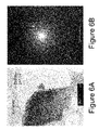
- FIG. 6A is a transmission electron microscope (TEM) image and FIG. 6B is a TEM diffraction pattern of a zeolite piece on BEST02 patterned substrate.
- TEM transmission electron microscope
- FIG. 7 is a comparative example showing a SEM image of zeolite crystals grown on BEST02 patterned wafer without performing the sonication and/or spin coating step.
- FIG. 8 is SEM image of zeolite crystals grown in BEST02 patterned structures using sonication and spin coating step (on part of the wafer substrate to visualize the filling effect).
- FIG. 9 is a SEM image of horizontally aligned zeolite crystal grown in trench structure in BEST02 patterned structures.
- FIG. 10 shows a phthalocyanine complex incorporated inside a VPI-5 zeolite crystal pore via in-situ synthesis.
- the Figure is taken from prior art reference Parton et al., (1994), Journal of Molecular Catalysis A: Chemical, 97: 183-186.
- FIG. 11 shows a Raman spectrum of the phthalocyanine incorporated VPI-5 after pyrolysis.
- FIG. 12A to FIG. 12C shows the test structure design according to the BEST02 as described above and used in the examples 1 to 5.
- FIG. 12A is a SEM photo illustrating a top view of the Si wafer substrate comprising the test structures
- FIG. 12B illustrates a more detailed top view of the wafer substrate illustrating the via holes
- FIG. 12C illustrates a cross section of the via holes in the Si substrate with a Ti/TiN contact electrode at the bottom of the vias.
- top, bottom, over, under and the like in the description and the claims are used for descriptive purposes and not necessarily for describing relative positions. It is to be understood that the terms so used are interchangeable under appropriate circumstances and that the preferred embodiments described herein are capable of operation in other orientations than described or illustrated herein.
- template as used herein is a broad term, and is to be given its ordinary and customary meaning to a person of ordinary skill in the art (and is not to be limited to a special or customized meaning), and refers without limitation to an organic zeolite-forming structure directing agent.
- This structure directing agent is typically an organic amine, such as tripropylamine (TPA), triethylamine, tetrapropylammonium hydroxide, tertraethylammonium hydroxide, triethyl-n-propylammonium hydroxide, 2-picoline, 3-picoline, 4-picoline, piperidine, N-methyldiethanolamine, and the like.
- TPA tripropylamine
- synthesis gel or “synthesis solution” as used herein are broad terms, and are to be given their ordinary and customary meaning to a person of ordinary skill in the art (and are not to be limited to a special or customized meaning), and refer without limitation to a zeolite synthesis composition gel or solution which may comprise a silicon source and an alkali source of inorganic or organic nature, and optionally a template molecule and hetero-elements such as Al, Ga, Ti, Fe, Co, Ge, P, or a mixture thereof, or to refer to a zeolite synthesis composition gel or solution which may comprise an aluminum and phosphorus source, as well as a source of acidity, and optionally a template molecule and hetero-elements such as Si, Ga, Ti, Fe, Co, Ge, or a mixture thereof.
- carbon nanostructures as used herein is a broad term, and is to be given its ordinary and customary meaning to a person of ordinary skill in the art (and is not to be limited to a special or customized meaning), and refers without limitation to both carbon nanoparticles as well as to carbon nanofibers and carbon nanotubes (CNTs) having a single-, double- or multi-wall structure referred to as SW-, DW- and MW-CNTs, respectively.
- porous structure as used herein is a broad term, and is to be given its ordinary and customary meaning to a person of ordinary skill in the art (and is not to be limited to a special or customized meaning), and refers without limitation to a microporous structure having pores in the range up to 2 nm, a mesoporous structure having pores in the range of 2 nm up to 50 nm or a macroporous structure having pores in the range of 50 nm and larger.
- zeolite crystals within a patterned structure (within the openings of the pattern).
- a method for providing zeolite crystals within patterned structures comprises at least the steps of: providing a substrate comprising in its top surface patterned structures (openings), impregnating a zeolite synthesis solution or gel onto the substrate followed by, applying mechanical forces to incorporate the synthesis solution into the patterned structures, applying hydrothermal conditions to crystallize the zeolite synthesis solution to form zeolite crystals, rinsing and drying the substrate, and optionally applying additional mechanical forces to remove non-incorporated or non-attached zeolite crystals.
- FIG. 1A is a flowchart 10 illustrating the different processing steps to synthesize zeolite crystals within patterned structures according to a preferred embodiment of the first aspect.
- a first step 11 the synthesis gel suitable for forming zeolite crystals and a substrate (e.g. wafer) comprising patterned structures (openings) in its top surface are provided according to state of the art methods.
- the synthesis gel is contacted with the substrate by known methods such as immersion (dipping) of the substrate in the synthesis gel or coating of the synthesis gel onto the top surface of the substrate.
- mechanical forces such as sonication and/or vibration are used to incorporate the synthesis solution into the patterned structures.
- step 14 hydrothermal conditions are applied (heating) to crystallize the zeolite synthesis solution to form zeolite crystals within the patterned structures.
- step 15 the substrate comprising the zeolite crystals is rinsed and dried.
- step 16 additional mechanical forces can be applied to remove non-incorporated or non-attached zeolite crystals from the substrate.
- the step of performing hydrothermal conditions (heating) to crystallize the zeolite synthesis solution to form zeolite crystals may be performed in a stainless steel autoclave 60 as illustrated in FIG. 3 .
- the experimental set-up of FIG. 3 comprises a Teflon substrate holder 62 on which a wafer piece (substrate comprising the patterned structure) is placed.
- the bottom of the reactor is filled with the synthesis gel 53 in which the wafer piece or substrate is immersed.
- FIG. 9 is a SEM image of a horizontally aligned zeolite crystal grown in an (horizontal) trench structure in BEST02 pattern.
- a substrate comprising patterned structures (openings) wherein said patterned structures comprise zeolite crystals and the zeolite crystals have an orientation in the direction defined by the confinement of the patterned structures is disclosed.
- the patterned structures may be trenches or via holes in a semiconductor device.
- the first aspect as described in a first preferred embodiment can be accomplished to form elongated carbon nanostructures (e.g. carbon nanotubes) within the pores of the zeolite crystals as described below in further preferred embodiments.
- the growth of these carbon nanostructures is performed by heating the zeolite crystals formed according to the first embodiment in the presence of a carbon comprising gas at a temperature range 350-1000° C.
- a method for growing (aligned) carbon nanostructures within the pores of zeolite crystals within patterned structures comprises at least the steps of: providing a substrate comprising in its top surface patterned structures (openings), impregnating a zeolite synthesis solution or gel onto the substrate followed by, applying mechanical forces to incorporate the synthesis solution into the patterned structures, applying hydrothermal conditions to crystallize the zeolite synthesis solution to form zeolite crystals, rinsing and drying the substrate, and optionally applying additional mechanical forces to remove non-incorporated or non-attached zeolite crystals, and heating the zeolite crystals in the presence of an inert gas or a mixture of an inert gas and a carbon containing gas at a temperature between 350° C.-1000° C. to grow the carbon nanostructures
- FIG. 1B is a flowchart 20 illustrating the preferred processing steps to first synthesize zeolite crystals within patterned structures followed by carbon nanostructure growth in the pores of the zeolite crystals according to preferred embodiments of the first aspect.
- a first step 21 the synthesis gel suitable for forming zeolite crystals and a substrate (e.g. wafer) comprising patterned structures (openings) in its top surface are provided according to state of the art methods.
- the synthesis gel is contacted with the substrate by known methods such as immersion (dipping) of the substrate in the synthesis gel or coating of the synthesis gel onto the top surface of the substrate.
- step 23 mechanical forces such as sonication and/or vibration are used to incorporate the synthesis solution into the patterned structures.
- hydrothermal conditions are applied (heating) to crystallize the zeolite synthesis solution to form zeolite crystals within the patterned structures.
- step 25 the substrate comprising the zeolite crystals is rinsed and dried. Additionally (optional) to step 25 mechanical forces can be applied to remove non-incorporated or non-attached zeolite crystals from the substrate.
- step 26 the zeolite crystals are heated in the presence of a carbon comprising gas at temperatures preferably in the range of 350° C. up to 1000° C.
- a substrate comprising patterned structures (openings) wherein said patterned structures comprise zeolite crystals and further comprise carbon nanostructures within the pores of the zeolite crystals and wherein the carbon nanostructures have an orientation in the direction defined by the confinement of the patterned structures is disclosed.
- the patterned structures may be trenches or via holes in a semiconductor device.
- methods are provided to form carbon nanostructures within the pores of zeolite crystals by first incorporating an organo-metal complex in the pores of the zeolite crystals and then performing a thermal treatment to grow carbon nanostructures.
- the improved method gives rise to significantly higher yields of intraporous nanocarbon growth compared to the prior art techniques.
- the organo-metal complex may be introduced in the zeolite crystal pores by impregnation or in-situ synthesis.
- the organo-metal complex of the preferred embodiments is preferably a (metallo)-phthalocyanine complex.
- Phthalocyanines may be incorporated in extra large pore zeolites such as VFI type zeolites and can be converted into carbon nanostructures under pyrolysis conditions.
- Preferred examples of suitable phthalocyanine complexes are Ni—, Fe—, Co—, or even H2-phthalocyanine complexes.
- Fe-phthalocyanine may be added to the zeolite by evaporating a solid source or precursor of phthalocyanine and Fe which will recombine within the porous structure of the zeolite crystal to form a Fe-phthalocyanine within the pores of the zeolite crystal.
- the stacking of the phthalocyanine complexes within the pores of the zeolite crystal is responsible for the necessary high carbon density for intraporous nanotube growth, and also the optional presence of transition metal catalyst.
- the improved method to grow the carbon nanostructures (e.g. CNT) within the pores of a zeolite crystal comprises at least the steps of: providing a zeolite synthesis solution or gel followed by, applying hydrothermal conditions to crystallize the zeolite synthesis solution to form zeolite crystals, heating the zeolite crystals and evaporating or impregnating a solid source or precursor of phthalocyanine and a metal at a temperature between room temperature up to 400° C.
- the phthalocyanine and the metal form a metal-phthalocyanine complex within the pores of the zeolite crystals, growing carbon nanostructures using the metal-phthalocyanine complex as an initiator by heating at a temperature between 350-1000° C.
- FIG. 1C is a flowchart 30 illustrating the processing steps to form carbon nanostructures within the pores of zeolite crystals by first incorporating an organo-metal complex in the pores of the zeolite crystals and then performing a thermal treatment to grow carbon nanostructures according to preferred embodiments of the second aspect.
- a synthesis gel suitable for forming zeolite crystals is provided according to state of the art methods.
- hydrothermal conditions are applied (heating) to crystallize the zeolite synthesis solution to form zeolite crystals.
- step 33 the zeolite crystals are heated and a solid source or precursor of phthalocyanine and a metal are evaporated and impregnated in the pores of the zeolite structure, preferably in the temperature range of room temperature up to 400° C.
- step 34 carbon nanostructures are grown using the metal-phthalocyanine complex as an initiator by heating at a temperature between 350-1000° C.
- hydrocarbon or CO gas can be added to the reactor in step 34 to initiate the growth of carbon nanostructures.
- FIG. 10 shows a phthalocyanine complex 81 incorporated inside a VPI-5 zeolite crystal 70 pore via in-situ synthesis.
- the Figure is taken from prior art reference Parton et al., (1994), Journal of Molecular Catalysis A: Chemical, 97: 183-186.
- FIG. 11 shows a Raman spectrum of the phthalocyanine incorporated VPI-5 after pyrolysis.
- the improved method to grow the carbon nanostructures (e.g. CNT) within the pores of a zeolite crystal according to the second aspect is compatible with the method to grow zeolite crystals within patterned structures as described in embodiments of the first aspect above.
- the method according to the second aspect to grow carbon nanostructures within the pores of a zeolite crystal using metal-organo complexes can be combined with the method according to the first aspect to provide zeolite crystals in a patterned structure.
- a preferred embodiment utilizes preferred method steps used to form elongated carbon nanostructures (e.g. carbon nanotubes) within the pores of the zeolite crystals situated in a patterned structure.
- a method for growing (aligned) carbon nanostructures within the pores of zeolite crystals within patterned structures comprises at least the steps of: providing a substrate comprising in its top surface patterned structures (openings), impregnating a zeolite synthesis solution or gel onto the substrate followed by, applying mechanical forces to incorporate the synthesis solution into the patterned structures, applying hydrothermal conditions to crystallize the zeolite synthesis solution to form zeolite crystals, rinsing and drying the substrate, and optionally applying additional mechanical forces to remove non-incorporated or non-attached zeolite crystals, heating the zeolite crystals and evaporating or impregnating a solid source or precursor of phthalocyanine and a metal at a temperature between 0° C.-400° C.
- the phthalocyanine and the metal are forming a metal-phthalocyanine complex within the pores of the zeolite crystals, and growing carbon nanostructures using the metallo-phthalocyanine complex as an initiator by heating at a temperature between 350-1000° C.
- FIG. 1D is a flowchart 40 illustrating the preferred processing steps to first synthesize zeolite crystals within patterned structures followed by growth of carbon nanostructures in the pores of the zeolite crystals according to preferred embodiments.
- a first step 41 the synthesis gel suitable for forming zeolite crystals and a substrate (e.g. wafer) comprising patterned structures (openings) in its top surface are provided according to state of the art methods.
- the synthesis gel is contacted with the substrate by known methods such as immersion (dipping) of the substrate in the synthesis gel or coating of the synthesis gel onto the top surface of the substrate.
- step 43 mechanical forces such as sonication and/or vibration are used to incorporate the synthesis solution into the patterned structures.
- hydrothermal conditions are applied (heating) to crystallize the zeolite synthesis solution to form zeolite crystals within the patterned structures.
- step 45 the substrate comprising the zeolite crystals is rinsed and dried. Additionally (optional) to step 45 additional mechanical forces can be applied to remove non-incorporated or non-attached zeolite crystals from the substrate.
- step 46 the zeolite crystals are heated and a solid source or precursor of phthalocyanine and a metal are evaporated or impregnated at a temperature between 0° C. up to 400° C.
- step 47 carbon nanostructures are grown within the pores of the zeolite crystals using the metallo-phthalocyanine complex as an initiator by heating at a temperature between 350° C.-1000° C.
- FIG. 9 illustrates (SEM image) a horizontally aligned zeolite crystal 53 having carbon nanostructures 54 within the pore of the zeolite crystal grown in trench structure 51 in BEST02 patterned structures.
- a substrate comprising patterned structures (openings) wherein said patterned structures comprise zeolite crystals and further comprise carbon nanostructures within the pores of the zeolite crystals and wherein the carbon nanostructures have an orientation in the direction defined by the confinement of the patterned structures.
- the substrate comprising patterned structures (openings) wherein said patterned structures comprise zeolite crystals and further comprise carbon nanostructures within the pores of the zeolite crystals and wherein the carbon nanostructures have an orientation in the direction defined by the confinement of the patterned structures according to preferred embodiments of the first and second aspect may be used as interconnect structures in a semiconductor device.
- FIGS. 2A and 2B illustrate a cross section of a substrate 50 having patterned structures 51 (openings) e.g. a BEST02 pattern with impregnated synthesis gel 52 on top of the substrate 51 .
- FIG. 2C illustrates a cross section of the substrate 50 having patterned structures 51 after sonication (vibration) and hydrothermal treatment to obtain zeolite crystals 53 inside the patterned structures 51 .
- FIG. 2D illustrates a cross section of the substrate having patterned structures 51 filled with zeolite crystals 53 after performing pyrolysis to obtain carbon nanostructures 54 inside the pores of the zeolite crystals 53 .
- the substrate may be any suitable substrate which is chosen in function of further applications.
- the substrate may be a semiconductor substrate such as a Si or Ge wafer.
- the patterned structures may be trenches or via holes which may be patterned in a dielectric layer having a k value lower than 5 .
- FIG. 12A to FIG. 12C shows a patterned structure design (a Si wafer having vias etched in a dielectric layer deposited on top of the wafer) according to the BEST02 test structure and used in the examples 1 to 5.
- FIG. 12A is a SEM photo illustrating a top view of the Si wafer substrate 80 comprising the test structures
- FIG. 12B illustrates a more detailed top view of the wafer substrate 80 illustrating the via holes 81 etched in a dielectric layer 82 .
- FIG. 12C illustrates a cross section of the via holes 81 in the Si substrate with a Ti/TiN contact electrode at the bottom of the vias 81 .
- suitable dielectric layers 82 are silicon dioxide and other state of the art low-k materials such as Black Diamond (Applied Materials).
- the patterning of the structures may be achieved using a combination of photolithographic imaging and (anisotropic) dry etching.
- the trenches and vias have preferably a diameter in the range of 50 nm up to 300 nm. Trenches have an aspect ratio (length/depth) greater than 1 whereas vias have an aspect ratio (length/depth) smaller than 1.
- the vias have preferably a width in the range of 1 ⁇ m up to 10 ⁇ m and a depth into the substrate in the range of 10 ⁇ m up to 100 ⁇ m. More preferred said deep vias are high aspect ratio vias having width of 5 ⁇ m and a depth of 50 ⁇ m.
- the patterned structure may be a single level mask structure with vias ranging from 50 nm up to 300 nm in diameter.
- the vias may land on a single common bottom electrode that can be made from a suite of different materials.
- An example of a suitable bottom contact electrode material is TiN.
- the zeolite synthesis solution or gel may comprise a silicon source and an alkali source of inorganic or organic nature, and optionally a template molecule and hetero-elements such as Al, Ga, Ti, Fe, Co, Ge, P, or a mixture thereof.
- the zeolite synthesis solution or gel may comprise an aluminum and phosphorus source, as well as a source of acidity, and a template molecule and optionally hetero-elements such as Si, Ga, Ti, Fe, Co, Ge, or a mixture thereof.
- SAPO-5 zeolite type material also referred to as AFI type
- aluminum-isopropoxide is used as an aluminum source
- phosphoric acid as a phosphorus source
- TPA tripropylamine
- Aerosil200 Degussa
- the synthesis gel is preferably a water-based solution; alcohols such as ethanol may be added to improve the wetability of the gel.
- An optimized synthesis gel for a silico-aluminophosphate may have the following composition:1 Al2O3:0.99 P2O5:1.2 TPA:400 H2O:20 Ethanol:0.01 SiO2.
- the organo-metal complex used for impregnation or in-situ synthesis in the zeolite pores, may consist of a transition metal in comprising Fe, Ni or Co and any organic ligand that sterically can be accommodated in the zeolite pores.
- the zeolite can be a crystalline porous material with parallel pores, preferably with one of the following structure types, as defined by the International Zeolite Association: AFI, VFI type material.
- AFI International Zeolite Association
- VFI type material
- the mechanical forces used to incorporate the synthesis gel are selected from sonication, vibration and/or spin-coating.
- Sonication may be used to incorporate the synthesis gel into the patterned structures, suitable sonication condition are e.g. 15 minutes at 47 kHz.
- Spin-coating may be used to remove excess of synthesis gel from the substrate, suitable spin-coating condition are e.g. 15000 rpm for 10 seconds.
- the hydrothermal treatment is used to crystallize the synthesis gel and thereby forming (ordered) zeolite crystals.
- Suitable hydrothermal conditions comprise the heating of the substrate under autogeneous pressure for 2-48 h at 100-200° C., more preferably for 14-15 h at 150-180° C.
- the rinsing and drying is performed using doubly-distilled water.
- the additional mechanical forces needed to remove non-incorporated or non-attached zeolite crystals is performed using sonication.
- the substrate is preferably again thoroughly rinsed with doubly-distilled water.
- the step of growing the carbon nanostructures is such that vertical growth of carbon nanostructures is achieved in a via (vertical hole) and horizontal growth of carbon nanostructures is achieved in a trench (horizontal line).
- the step of growing the carbon nanostructures is achieved using high temperature pyrolysis conditions.
- the carbon source needed for the nanostructure synthesis may originate from the organic template molecule used for zeolite synthesis.
- a carbon containing gas may be added to the atmosphere under pyrolysis conditions (possibly in high pressure conditions).
- organo-metal complexes within the porous structure of the zeolite crystal such as metal phthalocyanine complexes leading to a stacking of these organo-metal complexes inside the zeolite pores.
- the pyrolysis step used to grow carbon nanostructures is performed within a thermal reactor e.g. a furnace.
- the reactor must be capable of heating the zeolite crystals to a temperature up to 1000° C.
- the thermal reactor preferably includes a chamber that can be maintained at vacuum or at a desired pressure, and further includes means for enabling a gas flow into the chamber.
- Preferred pyrolysis may be the heating of the zeolite crystals under a flow of inert gas. Then keep the zeolite crystals isothermal at 400-900° C. for 10-3600 min, more preferably at 550° C. for 50-150 min.
- An optimized synthesis gel has the following composition: 1 Al 2 O 3 :0.99 P 2 O 5 :1.2 TPA:400 H 2 O:20 Ethanol:0.01 SiO 2 .
- a patterned wafer piece, with via holes of 50 nm-200 nm diameter, is immersed in the synthesis gel, thereafter beaker with both synthesis gel and wafer piece are put in a sonication bath for 15′ at 47 kHz.
- Excess synthesis gel is removed via a spin coating procedure, using 15000 rpm for 10 s.
- the crystallization is carried out under autogeneous pressure for 14h-15 h at 180° C. Afterwards, the autoclaves are cooled in air, and the wafer piece is thoroughly rinsed with doubly-distilled water. The wafer piece is again sonicated to remove the non attached crystals, and again thoroughly rinsed with doubly-distilled water.
- An optimized synthesis gel has the following composition: 1 Al 2 O 3 :0.99 P 2 O 5 :1.2 TPA:400 H 2 O:20 Ethanol:0.01 SiO 2 .
- a patterned wafer piece, with via holes of 50 nm-200 nm diameter, is immersed in the synthesis gel. The crystallization is carried out under autogeneous pressure for 14 h-15 h at 180° C.
- FIG. 7 is a comparative example showing a SEM image of zeolite crystals grown on BEST02 patterned wafer without performing the sonication and/or spin coating step.
- An optimized synthesis gel has the following composition: 1 Al 2 O 3 :0.99 P 2 O 5 :1.2 TPA:400 H 2 O:20 Ethanol:0.01 SiO 2 .
- a patterned wafer piece, with via holes of 50 nm-200 nm diameter, is immersed in the synthesis gel, thereafter beaker with both synthesis gel and wafer piece are put in a sonication bath for 15′ at 47 kHz.
- the crystallization is carried out under autogeneous pressure for 14 h-15 h at 180° C. Afterwards, the autoclaves are cooled in air, and the wafer piece is thoroughly rinsed with doubly-distilled water. The wafer piece is again sonicated to remove the non attached crystals, and again thoroughly rinsed with doubly-distilled water.
- zeolite crystals grow on top of the wafer, forming a crust. As there is no depletion of nutrients during zeolite growth, and once confinement effect of via hole or trench is gone, large crystal growth can be seen. The orientation of the crystal seems to be directed by the pattern.
- the cohesion of the zeolite crystals is larger than the adhesion zeolite-wafer, therefore zeolite “roots” are for a large part removed from the via holes during post synthesis sonication. It can be seen that filling degree is very good when looking at a bottom side of zeolite crust, but as large crystals get detached during post synthesis sonication, they take their “roots” with them.
- Si-VPI-5 was successful using a slightly adapted procedure from Martens et al. [Catalysis Letters, (12) 367-374, 1991]. From a gel with composition 1 Al 2 O 3 :1.05 P 2 O 5 :2 TBA:0.2 DPTA:40 H 2 O:0.2 SiO 2 , via sol-gel chemistry, pure Si-VPI-5 phase is obtained. First the Al-source, pseudoboehmite, and the P-source, phosphoric acid, are hydrated with 60% and 40% of the water, respectively. The diluted phosphoric acid is added dropwise to the Al-sol. The gel is put in a hot-water bath (95° C.) for 25 minutes, and is then further aged for 165 minutes at room temperature.
- a hot-water bath 95° C.
- the templates are added dropwise.
- the Si is added in the form of Ludox AS-40 in a single shot.
- the gel is gently stirred for another 5 minutes, and is the loaded in stainless steel autoclaves, together with a Teflon bead.
- the autoclaves are heated to 150° C. for 18 h while rotating.
- the obtained solid is separated by centrifugation, and then thoroughly washed with water.
- the powder is dried in an oven at 30° C. Phthalocyanines are incorporated via in situ chemical synthesis.
- the VPI-5 powder is thoroughly mixed with 1,2-dicyanobenzene and ferrocene. This mixture is heated under He for 4 hours at 250° C.
- the material obtained is Soxhlet extracted successively with acetone, dimethylformamide and again acetone until solvent remained colorless. This powder is then heated under He flow for 2 hours at 600° C. to obtain carbon nanostructures in the VPI-5 pores.
- Carbon nanostructures are achieved up to 10 wt % without addition of carbon containing gas during pyrolysis, which outperforms prior art [US2006/0051674].
- Pore filling degrees of nanocarbon have been reported up tot 18% nanocarbon without addition of carbon containing gas during pyrolysis procedure, and up to 28% with addition of carbon containing gas during pyrolysis.
- pyrolysis of incorporated Fe-phthalocyanine yields 60% pore filling degree of nanocarbon.
- Raman spectroscopy gives low I D /I G ratio of 0.25, indicating high quality of formed nanocarbon. Also a RBM band, typical for the presence of SWCNT, is detected. Diameters calculated from RBM agree very well with pore sizes of VFI framework.
- the patterned structure used here is a single level mask structure with vias ranging from 50-300 nm in diameter and with 3 different pitches.
- the vias land on a single common bottom electrode that can be made from a suite of different materials.
- TiN is a suitable material and is chosen as bottom contact material in the test structure. This simple test structure design therefore facilitates the vertical CNT growth in zeolites confined within the vias, their integration with the bottom contact and top-metallization to enable consequent electrical testing of the CNT.
- test structure includes: via (contact) holes 50-300 nm diameter; and use of a standard process meaning that vias are etched only down to 150 nm diameter.
- Each reticle matrix contains three arrays of via holes of different pitch: dense contact holes, with via pitch equal to 2 times the via diameter ⁇ 8000 (300 nm) to 17000 (150 nm) rows, 81 column; semi-dense contact holes, with via pitch equal to 2.4 times the via diameter ⁇ 7000 (300 nm) to 14000 (150 nm) rows, 96-98 columns; and isolated contact holes, with via pitch equal to 6 times the via diameter ⁇ 2400 (300 nm) to 4800 (150 nm) rows, 281 columns.
- FIG. 12A to FIG. 12C illustrates SEM pictures of the test structure design according to the BEST02 design as described above and used in the examples 1 to 5.
Abstract
Description
Claims (20)
Priority Applications (1)
| Application Number | Priority Date | Filing Date | Title |
|---|---|---|---|
| US12/358,063 US7790600B2 (en) | 2008-02-15 | 2009-01-22 | Synthesis of zeolite crystals and formation of carbon nanostructures in patterned structures |
Applications Claiming Priority (5)
| Application Number | Priority Date | Filing Date | Title |
|---|---|---|---|
| US2928608P | 2008-02-15 | 2008-02-15 | |
| EP08155596A EP2096081B1 (en) | 2008-02-15 | 2008-05-02 | Synthesis of zeolite crystals and formation of carbon nanostructures in patterned structures |
| EP08155596 | 2008-05-02 | ||
| EP08155596.3 | 2008-05-02 | ||
| US12/358,063 US7790600B2 (en) | 2008-02-15 | 2009-01-22 | Synthesis of zeolite crystals and formation of carbon nanostructures in patterned structures |
Publications (2)
| Publication Number | Publication Date |
|---|---|
| US20090243103A1 US20090243103A1 (en) | 2009-10-01 |
| US7790600B2 true US7790600B2 (en) | 2010-09-07 |
Family
ID=39735409
Family Applications (1)
| Application Number | Title | Priority Date | Filing Date |
|---|---|---|---|
| US12/358,063 Expired - Fee Related US7790600B2 (en) | 2008-02-15 | 2009-01-22 | Synthesis of zeolite crystals and formation of carbon nanostructures in patterned structures |
Country Status (4)
| Country | Link |
|---|---|
| US (1) | US7790600B2 (en) |
| EP (2) | EP2098484A1 (en) |
| JP (1) | JP2009196884A (en) |
| AT (1) | ATE516247T1 (en) |
Cited By (3)
| Publication number | Priority date | Publication date | Assignee | Title |
|---|---|---|---|---|
| US20130020280A1 (en) * | 2010-04-13 | 2013-01-24 | Toyota Jidosha Kabushiki Kaisha | Method of manufacturing fuel cell |
| US9425000B2 (en) | 2012-10-30 | 2016-08-23 | Industrial Technology Research Institute | Porous carbon material and manufacturing method thereof and supercapacitor |
| US10243156B2 (en) | 2017-03-16 | 2019-03-26 | International Business Machines Corporation | Placement of carbon nanotube guided by DSA patterning |
Families Citing this family (10)
| Publication number | Priority date | Publication date | Assignee | Title |
|---|---|---|---|---|
| CN101948106B (en) * | 2010-09-28 | 2013-03-27 | 华东理工大学 | Preparation method of blocky porous carbon with high specific surface area |
| CN102887875B (en) * | 2011-07-21 | 2014-08-06 | 中国石油化工股份有限公司 | Method for preparing epoxypropane |
| CN103449403A (en) * | 2013-08-26 | 2013-12-18 | 中国科学院上海硅酸盐研究所 | Method for manufacturing nitrogen-doped multi-wall carbon nano tube |
| US8889222B1 (en) * | 2013-12-03 | 2014-11-18 | Advenira Enterprises, Inc. | Coating material distribution using simultaneous rotation and vibration |
| CN106082264A (en) * | 2016-06-08 | 2016-11-09 | 清华大学 | A kind of multilevel hierarchy molecular sieve bar array, preparation method and applications |
| CN107814393B (en) * | 2017-12-04 | 2019-12-27 | 上海绿强新材料有限公司 | Method for rapidly crystallizing and synthesizing EMT molecular sieve |
| CN109166682B (en) * | 2018-08-30 | 2020-04-28 | 深圳大学 | Magnetic porous carbon material and preparation method thereof |
| KR102298625B1 (en) * | 2019-10-04 | 2021-09-06 | 전남대학교산학협력단 | High-throughput Synthesis Method of Zeolite |
| CN113929112B (en) * | 2020-06-29 | 2023-08-29 | 中国石油化工股份有限公司 | ATS type silicon-aluminum molecular sieve, preparation method and application thereof |
| US20230271842A1 (en) * | 2020-08-05 | 2023-08-31 | Sankar Nair | Zeolite nanotubes and methods of making and use thereof |
Citations (6)
| Publication number | Priority date | Publication date | Assignee | Title |
|---|---|---|---|---|
| US6620402B2 (en) * | 1999-12-06 | 2003-09-16 | Haldor Topsoe A.S | Method of preparing zeolite single crystals with straight mesopores |
| US7005118B2 (en) * | 2002-07-25 | 2006-02-28 | Instituto Mexicano Del Petroleo | Synthetic mesoporous material with radially assembled nanotubes |
| US20060216221A1 (en) * | 2003-03-20 | 2006-09-28 | Lee Cheol J | Massive synthesis method of double-walled carbon nanotubes using the vapor phase growth |
| US7303989B2 (en) * | 2004-11-22 | 2007-12-04 | Intel Corporation | Using zeolites to improve the mechanical strength of low-k interlayer dielectrics |
| US20080317631A1 (en) * | 2007-06-20 | 2008-12-25 | Reginald Conway Farrow | Nanotube Device and Method of Fabrication |
| US20100021650A1 (en) * | 2002-12-24 | 2010-01-28 | Sony Corporation | Method of manufacturing micro structure, and method of manufacturing mold material |
Family Cites Families (5)
| Publication number | Priority date | Publication date | Assignee | Title |
|---|---|---|---|---|
| JP2002526354A (en) * | 1998-09-28 | 2002-08-20 | ザイデックス コーポレイション | Method for producing carbon nanotubes as a functional element of a MEMS device |
| JP4212258B2 (en) * | 2001-05-02 | 2009-01-21 | 富士通株式会社 | Integrated circuit device and integrated circuit device manufacturing method |
| JP2003112052A (en) * | 2001-10-03 | 2003-04-15 | Toyota Motor Corp | Hydrogen generating catalyst |
| US7465519B2 (en) | 2004-09-03 | 2008-12-16 | The Hongkong University Of Science And Technology | Lithium-ion battery incorporating carbon nanostructure materials |
| JP4481853B2 (en) * | 2005-03-18 | 2010-06-16 | 富士通株式会社 | Manufacturing method of carbon nanotube device |
-
2008
- 2008-05-02 AT AT08155596T patent/ATE516247T1/en not_active IP Right Cessation
- 2008-05-02 EP EP09156708A patent/EP2098484A1/en not_active Withdrawn
- 2008-05-02 EP EP08155596A patent/EP2096081B1/en not_active Not-in-force
-
2009
- 2009-01-22 US US12/358,063 patent/US7790600B2/en not_active Expired - Fee Related
- 2009-02-13 JP JP2009031535A patent/JP2009196884A/en active Pending
Patent Citations (6)
| Publication number | Priority date | Publication date | Assignee | Title |
|---|---|---|---|---|
| US6620402B2 (en) * | 1999-12-06 | 2003-09-16 | Haldor Topsoe A.S | Method of preparing zeolite single crystals with straight mesopores |
| US7005118B2 (en) * | 2002-07-25 | 2006-02-28 | Instituto Mexicano Del Petroleo | Synthetic mesoporous material with radially assembled nanotubes |
| US20100021650A1 (en) * | 2002-12-24 | 2010-01-28 | Sony Corporation | Method of manufacturing micro structure, and method of manufacturing mold material |
| US20060216221A1 (en) * | 2003-03-20 | 2006-09-28 | Lee Cheol J | Massive synthesis method of double-walled carbon nanotubes using the vapor phase growth |
| US7303989B2 (en) * | 2004-11-22 | 2007-12-04 | Intel Corporation | Using zeolites to improve the mechanical strength of low-k interlayer dielectrics |
| US20080317631A1 (en) * | 2007-06-20 | 2008-12-25 | Reginald Conway Farrow | Nanotube Device and Method of Fabrication |
Non-Patent Citations (17)
| Title |
|---|
| Balkus Jr. et al. Studies in Surface Science and Catalysis, 154, 903-910, 2004. |
| Burghard, M. "Carbon Nanotubes by Quantitative Solid-State Conversion of an Organometallic Precursor" Angewandte Chemie International Edition, vol. 42, No. 48, Dec. 10, 2003, pp. 5929-5930. |
| Corma et al. Microelectronic Engineering (2008), doi: 10.1016/j.mee.2008.01.061. |
| Davis, M. "Ordered Porous Materials for Emerging Applications" Nature, vol. 417, Jun. 20, 2002, pp. 813-821. |
| Deng et al. "Molecular sieve encapsulated single walled carbon nanotubes" The Electrochemical Society, Mar. 23, 2006, URL: http://www.electrochem.org/dl/ma/203/pdfs/1468.pdf. |
| Hayashi et al. Nano Letters, 3, 887-889, 2003. |
| Kyotani et al. Chemistry of Materials, 8, 2109-2113, 1996. |
| Parton et al. Journal of Molecular Catalysis A: Chemical, 97: 183-186, 1994. |
| Qin et al. Nature, 408, 50, 2000. |
| Sun et al. "Synthesis and Raman characterization of mono-sized single-wall carbon nanotubes in one-dimensional channels of AIPO4-5 crystals" Applied Physics A Materials Science & Processing, vol. 69, No. 4, Jun. 24, 1999, pp. 381-384. |
| Tang et al. "Mono-sized single-wall carbon nanotubes formed in channels of AIPO4-5 single crystal" Appl. Phys. Lett. 73, 2287 (1998). |
| Tang et al. Applied Physics Letters, 73, 2287-2289, 1998. |
| Urban et al. "Production of carbon Nanotubes inside the pores of mesoporous silicates" Chemical Physics Letters, vol. 359, Apr. 16, 2002, pp. 95-100. |
| Urban et al. Chemical Physics Letters, 359, 95-100, 2002. |
| Wang et al. "Single-walled 4 Å carbon nanotube arrays" Nature, vol. 408, Nov. 2, 2000, pp. 50-51. |
| Wang et al. Nature, 408, 50-51, 2000. |
| Yu et al. "Efficient synthesis of carbon nanotubes over rare earth zeolites by thermal chemical vapor deposition at low temperatures" Diamond and Related Materials, vol. 15, No. 9, Sep. 2006, pp. 1261-1265. |
Cited By (5)
| Publication number | Priority date | Publication date | Assignee | Title |
|---|---|---|---|---|
| US20130020280A1 (en) * | 2010-04-13 | 2013-01-24 | Toyota Jidosha Kabushiki Kaisha | Method of manufacturing fuel cell |
| US9203101B2 (en) * | 2010-04-13 | 2015-12-01 | Toyota Jidosha Kabushiki Kaisha | Method of manufacturing fuel cell |
| US9425000B2 (en) | 2012-10-30 | 2016-08-23 | Industrial Technology Research Institute | Porous carbon material and manufacturing method thereof and supercapacitor |
| US10243156B2 (en) | 2017-03-16 | 2019-03-26 | International Business Machines Corporation | Placement of carbon nanotube guided by DSA patterning |
| US10374179B2 (en) | 2017-03-16 | 2019-08-06 | International Business Machines Corporation | Placement of carbon nanotube guided by DSA patterning |
Also Published As
| Publication number | Publication date |
|---|---|
| JP2009196884A (en) | 2009-09-03 |
| EP2098484A1 (en) | 2009-09-09 |
| US20090243103A1 (en) | 2009-10-01 |
| EP2096081A1 (en) | 2009-09-02 |
| EP2096081B1 (en) | 2011-07-13 |
| ATE516247T1 (en) | 2011-07-15 |
Similar Documents
| Publication | Publication Date | Title |
|---|---|---|
| US7790600B2 (en) | Synthesis of zeolite crystals and formation of carbon nanostructures in patterned structures | |
| KR101016763B1 (en) | Process for producing single-walled carbon nanotube | |
| Lin et al. | Formation of mesoporous silica nanotubes | |
| US8367034B2 (en) | Methods for preparing single-walled carbon nanotubes | |
| US7776398B2 (en) | Process for forming mesostructured material and process for controlling orientation of tubular mesopores | |
| US7842387B2 (en) | Methods for growing and harvesting carbon nanotubes | |
| Cambré et al. | Nanotube‐based 1D heterostructures coupled by van der Waals forces | |
| KR20030077425A (en) | Aligned carbon nanotube films and a process for producing them | |
| US11192789B2 (en) | Fibrous carbon nanostructure dispersion liquid, method of producing same, and fibrous carbon nanostructure | |
| US20070084346A1 (en) | Nanostructures containing carbon nanotubes and methods of their synthesis and use | |
| KR102095282B1 (en) | Photoluminescent Carbon Nano-structure and Fabrication Method Thereof | |
| Lu et al. | Topotactic conversion of Ge-rich IWW zeolite into IPC-18 under mild condition | |
| JP3587373B2 (en) | Mesostructured thin film and method of manufacturing the same | |
| Mannering et al. | Engineering of microcage carbon nanotube architectures with decoupled multimodal porosity and amplified catalytic performance | |
| Carpena‐Núñez et al. | Zeolite Nanosheets Stabilize Catalyst Particles to Promote the Growth of Thermodynamically Unfavorable, Small‐Diameter Carbon Nanotubes | |
| JP2012532089A (en) | Method for forming single-walled carbon nanotube | |
| CN112978717A (en) | Method for shortening carbon nano tube | |
| JP2009269788A (en) | Method of synthesizing hollow zeolite, hollow zeolite and drug support comprising hollow zeolite | |
| WO2020123974A1 (en) | Fabrication of carbon-based nanostructures on metallic substrates, including aluminum-containing substrates | |
| JP2007070224A (en) | Composition containing single-walled carbon nanotube | |
| RU2397139C1 (en) | Method and device for continuous production of nanodispersed materials | |
| JP6762005B2 (en) | Method for manufacturing carbon nanotube aggregates | |
| Tripathi et al. | A Detailed Study on Carbon Nanotubes: Properties, Synthesis, and Characterization | |
| Zheng et al. | Efficient fabrication of single-wall carbon nanotube nanoreactors by defect-induced cutting | |
| KR100527382B1 (en) | Scanning probe microscopy tip using carbon nanotube with vertical growth and its method |
Legal Events
| Date | Code | Title | Description |
|---|---|---|---|
| AS | Assignment |
Owner name: INTERUNIVERSITAIR MICROELEKTRONICA CENTRUM VZW (IM Free format text: ASSIGNMENT OF ASSIGNORS INTEREST;ASSIGNORS:JACOBS, PIERRE;SELS, BERT;VAN NOYEN, JASPER;AND OTHERS;REEL/FRAME:022479/0049;SIGNING DATES FROM 20090212 TO 20090310 Owner name: KATHOLIEKE UNIVERSITEIT LEUVEN, K.U.LEUVEN R&D, BE Free format text: ASSIGNMENT OF ASSIGNORS INTEREST;ASSIGNORS:JACOBS, PIERRE;SELS, BERT;VAN NOYEN, JASPER;AND OTHERS;REEL/FRAME:022479/0049;SIGNING DATES FROM 20090212 TO 20090310 Owner name: INTERUNIVERSITAIR MICROELEKTRONICA CENTRUM VZW (IM Free format text: ASSIGNMENT OF ASSIGNORS INTEREST;ASSIGNORS:JACOBS, PIERRE;SELS, BERT;VAN NOYEN, JASPER;AND OTHERS;SIGNING DATES FROM 20090212 TO 20090310;REEL/FRAME:022479/0049 Owner name: KATHOLIEKE UNIVERSITEIT LEUVEN, K.U.LEUVEN R&D, BE Free format text: ASSIGNMENT OF ASSIGNORS INTEREST;ASSIGNORS:JACOBS, PIERRE;SELS, BERT;VAN NOYEN, JASPER;AND OTHERS;SIGNING DATES FROM 20090212 TO 20090310;REEL/FRAME:022479/0049 |
|
| AS | Assignment |
Owner name: IMEC,BELGIUM Free format text: "IMEC" IS AN ALTERNATIVE OFFICIAL NAME FOR "INTERUNIVERSITAIR MICROELEKTRONICA CENTRUM VZW";ASSIGNOR:INTERUNIVERSITAIR MICROELEKTRONICA CENTRUM VZW;REEL/FRAME:024200/0675 Effective date: 19840318 Owner name: IMEC, BELGIUM Free format text: "IMEC" IS AN ALTERNATIVE OFFICIAL NAME FOR "INTERUNIVERSITAIR MICROELEKTRONICA CENTRUM VZW";ASSIGNOR:INTERUNIVERSITAIR MICROELEKTRONICA CENTRUM VZW;REEL/FRAME:024200/0675 Effective date: 19840318 |
|
| FEPP | Fee payment procedure |
Free format text: PAYOR NUMBER ASSIGNED (ORIGINAL EVENT CODE: ASPN); ENTITY STATUS OF PATENT OWNER: LARGE ENTITY |
|
| CC | Certificate of correction | ||
| FPAY | Fee payment |
Year of fee payment: 4 |
|
| FEPP | Fee payment procedure |
Free format text: MAINTENANCE FEE REMINDER MAILED (ORIGINAL EVENT CODE: REM.) |
|
| LAPS | Lapse for failure to pay maintenance fees |
Free format text: PATENT EXPIRED FOR FAILURE TO PAY MAINTENANCE FEES (ORIGINAL EVENT CODE: EXP.); ENTITY STATUS OF PATENT OWNER: LARGE ENTITY |
|
| STCH | Information on status: patent discontinuation |
Free format text: PATENT EXPIRED DUE TO NONPAYMENT OF MAINTENANCE FEES UNDER 37 CFR 1.362 |
|
| FP | Lapsed due to failure to pay maintenance fee |
Effective date: 20180907 |