US7790574B2 - Boron diffusion in silicon devices - Google Patents
Boron diffusion in silicon devices Download PDFInfo
- Publication number
- US7790574B2 US7790574B2 US11/301,527 US30152705A US7790574B2 US 7790574 B2 US7790574 B2 US 7790574B2 US 30152705 A US30152705 A US 30152705A US 7790574 B2 US7790574 B2 US 7790574B2
- Authority
- US
- United States
- Prior art keywords
- wafer
- boric oxide
- boron
- oxide solution
- heating cycle
- Prior art date
- Legal status (The legal status is an assumption and is not a legal conclusion. Google has not performed a legal analysis and makes no representation as to the accuracy of the status listed.)
- Expired - Fee Related, expires
Links
- ZOXJGFHDIHLPTG-UHFFFAOYSA-N Boron Chemical compound [B] ZOXJGFHDIHLPTG-UHFFFAOYSA-N 0.000 title claims abstract description 46
- 229910052796 boron Inorganic materials 0.000 title claims abstract description 45
- 238000009792 diffusion process Methods 0.000 title claims abstract description 27
- XUIMIQQOPSSXEZ-UHFFFAOYSA-N Silicon Chemical compound [Si] XUIMIQQOPSSXEZ-UHFFFAOYSA-N 0.000 title claims description 19
- 229910052710 silicon Inorganic materials 0.000 title claims description 18
- 239000010703 silicon Substances 0.000 title claims description 18
- 229910011255 B2O3 Inorganic materials 0.000 claims abstract description 70
- JKWMSGQKBLHBQQ-UHFFFAOYSA-N diboron trioxide Chemical compound O=BOB=O JKWMSGQKBLHBQQ-UHFFFAOYSA-N 0.000 claims abstract description 70
- 238000000034 method Methods 0.000 claims abstract description 49
- 238000010438 heat treatment Methods 0.000 claims abstract description 48
- 230000008569 process Effects 0.000 claims abstract description 44
- KFZMGEQAYNKOFK-UHFFFAOYSA-N Isopropanol Chemical compound CC(C)O KFZMGEQAYNKOFK-UHFFFAOYSA-N 0.000 claims description 20
- 239000005388 borosilicate glass Substances 0.000 claims description 20
- KGBXLFKZBHKPEV-UHFFFAOYSA-N boric acid Chemical compound OB(O)O KGBXLFKZBHKPEV-UHFFFAOYSA-N 0.000 claims description 18
- 239000004327 boric acid Substances 0.000 claims description 18
- 239000002904 solvent Substances 0.000 claims description 13
- LFQSCWFLJHTTHZ-UHFFFAOYSA-N Ethanol Chemical compound CCO LFQSCWFLJHTTHZ-UHFFFAOYSA-N 0.000 claims description 12
- 229910000676 Si alloy Inorganic materials 0.000 claims description 9
- CFOAUMXQOCBWNJ-UHFFFAOYSA-N [B].[Si] Chemical compound [B].[Si] CFOAUMXQOCBWNJ-UHFFFAOYSA-N 0.000 claims description 9
- 238000004140 cleaning Methods 0.000 claims description 8
- 238000001704 evaporation Methods 0.000 claims description 8
- 230000008020 evaporation Effects 0.000 claims description 7
- 238000005507 spraying Methods 0.000 claims description 7
- 238000006243 chemical reaction Methods 0.000 claims description 6
- 239000011248 coating agent Substances 0.000 claims description 6
- 238000000576 coating method Methods 0.000 claims description 6
- 238000007598 dipping method Methods 0.000 claims description 5
- 238000009987 spinning Methods 0.000 claims description 5
- 230000002209 hydrophobic effect Effects 0.000 claims description 3
- 230000005661 hydrophobic surface Effects 0.000 claims description 3
- 235000012431 wafers Nutrition 0.000 description 90
- 239000000243 solution Substances 0.000 description 41
- 239000002019 doping agent Substances 0.000 description 10
- 238000004519 manufacturing process Methods 0.000 description 8
- VEXZGXHMUGYJMC-UHFFFAOYSA-N Hydrochloric acid Chemical compound Cl VEXZGXHMUGYJMC-UHFFFAOYSA-N 0.000 description 7
- VYPSYNLAJGMNEJ-UHFFFAOYSA-N Silicium dioxide Chemical compound O=[Si]=O VYPSYNLAJGMNEJ-UHFFFAOYSA-N 0.000 description 7
- XLYOFNOQVPJJNP-UHFFFAOYSA-N water Substances O XLYOFNOQVPJJNP-UHFFFAOYSA-N 0.000 description 7
- KRHYYFGTRYWZRS-UHFFFAOYSA-N Fluorane Chemical compound F KRHYYFGTRYWZRS-UHFFFAOYSA-N 0.000 description 6
- 238000002474 experimental method Methods 0.000 description 5
- 239000000356 contaminant Substances 0.000 description 4
- 239000000463 material Substances 0.000 description 4
- 235000012239 silicon dioxide Nutrition 0.000 description 4
- 230000005660 hydrophilic surface Effects 0.000 description 3
- 239000000377 silicon dioxide Substances 0.000 description 3
- 239000007921 spray Substances 0.000 description 3
- VHUUQVKOLVNVRT-UHFFFAOYSA-N Ammonium hydroxide Chemical compound [NH4+].[OH-] VHUUQVKOLVNVRT-UHFFFAOYSA-N 0.000 description 2
- QAOWNCQODCNURD-UHFFFAOYSA-N Sulfuric acid Chemical compound OS(O)(=O)=O QAOWNCQODCNURD-UHFFFAOYSA-N 0.000 description 2
- 238000013459 approach Methods 0.000 description 2
- 238000005530 etching Methods 0.000 description 2
- 238000012986 modification Methods 0.000 description 2
- 230000004048 modification Effects 0.000 description 2
- 238000002161 passivation Methods 0.000 description 2
- 238000012545 processing Methods 0.000 description 2
- 230000007704 transition Effects 0.000 description 2
- 238000009827 uniform distribution Methods 0.000 description 2
- KWYUFKZDYYNOTN-UHFFFAOYSA-M Potassium hydroxide Chemical compound [OH-].[K+] KWYUFKZDYYNOTN-UHFFFAOYSA-M 0.000 description 1
- 238000010521 absorption reaction Methods 0.000 description 1
- 238000003916 acid precipitation Methods 0.000 description 1
- 239000000908 ammonium hydroxide Substances 0.000 description 1
- 230000008901 benefit Effects 0.000 description 1
- 230000015572 biosynthetic process Effects 0.000 description 1
- 238000009835 boiling Methods 0.000 description 1
- 229910052810 boron oxide Inorganic materials 0.000 description 1
- 238000001816 cooling Methods 0.000 description 1
- 230000007547 defect Effects 0.000 description 1
- 238000011161 development Methods 0.000 description 1
- 238000010790 dilution Methods 0.000 description 1
- 239000012895 dilution Substances 0.000 description 1
- 238000009826 distribution Methods 0.000 description 1
- 230000005611 electricity Effects 0.000 description 1
- 239000003344 environmental pollutant Substances 0.000 description 1
- 239000002803 fossil fuel Substances 0.000 description 1
- 239000011521 glass Substances 0.000 description 1
- 230000007774 longterm Effects 0.000 description 1
- 230000007246 mechanism Effects 0.000 description 1
- 238000013082 photovoltaic technology Methods 0.000 description 1
- 231100000719 pollutant Toxicity 0.000 description 1
- 238000002360 preparation method Methods 0.000 description 1
- 230000001737 promoting effect Effects 0.000 description 1
- 239000010453 quartz Substances 0.000 description 1
- 238000005215 recombination Methods 0.000 description 1
- 230000006798 recombination Effects 0.000 description 1
- 239000007787 solid Substances 0.000 description 1
- 238000010792 warming Methods 0.000 description 1
Images


Classifications
-
- H—ELECTRICITY
- H01—ELECTRIC ELEMENTS
- H01L—SEMICONDUCTOR DEVICES NOT COVERED BY CLASS H10
- H01L21/00—Processes or apparatus adapted for the manufacture or treatment of semiconductor or solid state devices or of parts thereof
- H01L21/02—Manufacture or treatment of semiconductor devices or of parts thereof
- H01L21/04—Manufacture or treatment of semiconductor devices or of parts thereof the devices having at least one potential-jump barrier or surface barrier, e.g. PN junction, depletion layer or carrier concentration layer
- H01L21/18—Manufacture or treatment of semiconductor devices or of parts thereof the devices having at least one potential-jump barrier or surface barrier, e.g. PN junction, depletion layer or carrier concentration layer the devices having semiconductor bodies comprising elements of Group IV of the Periodic System or AIIIBV compounds with or without impurities, e.g. doping materials
- H01L21/22—Diffusion of impurity materials, e.g. doping materials, electrode materials, into or out of a semiconductor body, or between semiconductor regions; Interactions between two or more impurities; Redistribution of impurities
- H01L21/225—Diffusion of impurity materials, e.g. doping materials, electrode materials, into or out of a semiconductor body, or between semiconductor regions; Interactions between two or more impurities; Redistribution of impurities using diffusion into or out of a solid from or into a solid phase, e.g. a doped oxide layer
- H01L21/2251—Diffusion into or out of group IV semiconductors
- H01L21/2254—Diffusion into or out of group IV semiconductors from or through or into an applied layer, e.g. photoresist, nitrides
- H01L21/2255—Diffusion into or out of group IV semiconductors from or through or into an applied layer, e.g. photoresist, nitrides the applied layer comprising oxides only, e.g. P2O5, PSG, H3BO3, doped oxides
-
- H—ELECTRICITY
- H01—ELECTRIC ELEMENTS
- H01L—SEMICONDUCTOR DEVICES NOT COVERED BY CLASS H10
- H01L31/00—Semiconductor devices sensitive to infrared radiation, light, electromagnetic radiation of shorter wavelength or corpuscular radiation and specially adapted either for the conversion of the energy of such radiation into electrical energy or for the control of electrical energy by such radiation; Processes or apparatus specially adapted for the manufacture or treatment thereof or of parts thereof; Details thereof
- H01L31/18—Processes or apparatus specially adapted for the manufacture or treatment of these devices or of parts thereof
- H01L31/1804—Processes or apparatus specially adapted for the manufacture or treatment of these devices or of parts thereof comprising only elements of Group IV of the Periodic System
-
- Y—GENERAL TAGGING OF NEW TECHNOLOGICAL DEVELOPMENTS; GENERAL TAGGING OF CROSS-SECTIONAL TECHNOLOGIES SPANNING OVER SEVERAL SECTIONS OF THE IPC; TECHNICAL SUBJECTS COVERED BY FORMER USPC CROSS-REFERENCE ART COLLECTIONS [XRACs] AND DIGESTS
- Y02—TECHNOLOGIES OR APPLICATIONS FOR MITIGATION OR ADAPTATION AGAINST CLIMATE CHANGE
- Y02E—REDUCTION OF GREENHOUSE GAS [GHG] EMISSIONS, RELATED TO ENERGY GENERATION, TRANSMISSION OR DISTRIBUTION
- Y02E10/00—Energy generation through renewable energy sources
- Y02E10/50—Photovoltaic [PV] energy
- Y02E10/547—Monocrystalline silicon PV cells
-
- Y—GENERAL TAGGING OF NEW TECHNOLOGICAL DEVELOPMENTS; GENERAL TAGGING OF CROSS-SECTIONAL TECHNOLOGIES SPANNING OVER SEVERAL SECTIONS OF THE IPC; TECHNICAL SUBJECTS COVERED BY FORMER USPC CROSS-REFERENCE ART COLLECTIONS [XRACs] AND DIGESTS
- Y02—TECHNOLOGIES OR APPLICATIONS FOR MITIGATION OR ADAPTATION AGAINST CLIMATE CHANGE
- Y02P—CLIMATE CHANGE MITIGATION TECHNOLOGIES IN THE PRODUCTION OR PROCESSING OF GOODS
- Y02P70/00—Climate change mitigation technologies in the production process for final industrial or consumer products
- Y02P70/50—Manufacturing or production processes characterised by the final manufactured product
Definitions
- the primary device used for this process is the solar cell or photovoltaic device.
- Photovoltaic devices essentially create electrical current when exposed to sunlight.
- the photovoltaic technology is not without its problems as well. Chief of these is the high cost of manufacturing photovoltaic cells. Specifically, the high cost for manufacturing photovoltaic cells discourages their widespread use as other forms of energy are currently less expensive.
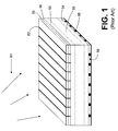
- FIG. 1 is a drawing of one example of a photovoltaic cell that may be created using a diffusion process as described herein according to an embodiment of the present invention
- FIG. 2 is a flow chart that illustrates steps of a process of boron diffusion in a wafer
- FIG. 3A is a drawing that illustrates the spinning of boric acid onto a wafer as part of the process depicted in FIG. 2 according to an embodiment of the present invention
- FIG. 3B is a drawing that illustrates the dipping of a wafer into boric acid in order to coat the wafer with boric acid as part of the process depicted in FIG. 2 according to an embodiment of the present invention
- FIG. 3C is a drawing that illustrates a spraying of boric acid onto a wafer as part of the process depicted in FIG. 2 according to an embodiment of the present invention
- FIG. 4A is a drawing illustrating a furnace employed to diffuse boron into a plurality of wafers that were coated with boric acid according to the process of FIG. 2 according to an embodiment of the present invention
- FIG. 4B is a drawing illustrating a box furnace employed to diffuse boron into a plurality of wafers that were coated with boric acid according to the process of FIG. 2 according to an embodiment of the present invention
- FIG. 4C is a drawing illustrating another furnace employed to diffuse boron into a plurality of wafers that were coated with boric acid according to the process of FIG. 2 according to an embodiment of the present invention
- FIG. 4D is a drawing illustrating a belt furnace employed to diffuse boron into a plurality of wafers that were coated with boric acid according to the process of FIG. 2 according to an embodiment of the present invention
- FIG. 5 is a graph illustrating a temperature curve of one example of a heating cycle employed in the process of FIG. 2 according to an embodiment of the present invention.
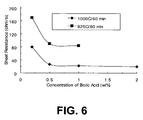
- FIG. 6 is a graph illustrating a sheet resistance of a wafer resulting from various concentrations of, for example, boric acid used in the process of FIG. 2 according to an embodiment of the present invention.
- the present invention provides for efficient means of diffusing boron into wafers by coating the wafers with a boric oxide solution and subjecting the wafers to a heating cycle with a fast heat ramp-up in order to release boron from the boric oxide solution for diffusion into the wafers as will be described.
- the photovoltaic cell is made of a silicon wafer 50 that has been doped with a base dopant material.
- the surfaces of the wafer 50 are then diffused with dopant material forming two diffused regions 53 and 54 .
- the diffused region 53 may form, for example, an emitter or p-n junction.
- the diffused region 54 may comprise, for example, a back surface field (BSF).
- BSF back surface field
- the wafer will have internal layers of diffused material and non-diffused material.
- the wafer may then be covered with a dielectric layers 56 on both sides that reduce surface recombination by passivating the surfaces.
- the final steps include the addition of an antireflection coating 59 to ensure the absorption of sunlight 61 and the introduction of contacts layers 63 and 66 which are connected to the diffused regions 53 which are used to connect the solar cell to an electrical load.
- one of the dopants that may be employed to create the diffused regions 53 ( FIG. 1 ) or 54 ( FIG. 1 ) comprises boron.
- the diffusion of boron into silicon wafers is performed in a controlled process during the manufacturing of solar cells.
- the depth of the diffusion of the boron, as well as, the concentration distribution of the boron diffused into a given silicon wafer is defined as the “dopant profile” of the wafer.
- the dopant profile of the wafer is specified so as to provide for a desired sheet resistance as can be appreciated by those with ordinary skill in the art. Since the concepts of a dopant profile and sheet resistance are well known by those skilled in the art, a detailed discussion of these concepts is omitted herein. The following discussion details a process by which boron is diffused into silicon wafers in order to achieve various desired dopant profiles as will be appreciated.
- the process starts with the cleaning or etching of the surfaces of one or more wafers so as to provide for either a hydrophilic or hydrophobic surface as desired that is substantially free of defects in/or contaminants to the extent possible.
- the surfaces are made hydrophilic so as to promote a uniform coating of boric oxide solution on the entire surface of the wafer when the boric oxide solution includes a solvent of water.
- the surfaces are made hydrophobic so as to promote a uniform coating of boric solution on the entire surface of the wafer when the boric oxide solution includes a solvent of ethanol or Isopropanol, etc.
- a solution such as 1:1:2 H 2 O;H 2 O 2 ;H 2 SO 4 , for example, is applied to the surface of the wafer. This is applied in order to remove organic contaminants as can be appreciated. Thereafter, a solution of hydrofluoric acid (1:10 or other dilution HF:H 2 O), for example, is applied to remove silicon dioxide components on the surface left by the prior treatment. Next, a solution such as hydrochloric acid (2:1:1 H 2 O:H 2 O 2 :HCl), for example, is applied to remove metallic contaminants that may be disposed on the surface.
- the application of the hydrofluoric acid and the hydrochloric acid may be repeatedly applied as desired or as deemed necessary. In this manner, the wafer is cleaned and a hydrophilic surface is left to promote the uniform distribution of boric acid along the surface itself. Alternatively, where it is desired that the surface of the wafer be hydrophobic, the cleaning with hydrofluoric acid and hydrochloric acid may be omitted.
- cleaning solutions or methods other than those discussed above may also be employed in cleaning or etching the wafer surface(s) in preparation for the diffusion of boron as described herein as can be appreciated by those with ordinary skill in the art.
- other solutions or methods may comprise, for example, Ammonium Hydroxide (H 2 O;H 2 O 2 ;NH 4 OH) in place of the 1:1:2 H 2 O;H 2 O 2 ;H 2 SO 4 .
- Potassium Hydroxide (KOH) may be employed to remove metallic contaminants resulting from sawing operations to create the wafers from larger sheets of silicon, etc.
- other cleaning techniques and solutions may be employed to create the hydrophilic or hydrophobic surfaces as desired.
- the wafer is dried. This may be done, for example, using a spin dryer or by virtue of isopropyl alcohol (IPA) boiling as can be appreciated. In addition, other approaches may be employed to dry the wafer after the cleaning process of block 100 above.
- IPA isopropyl alcohol
- an amount of boric oxide solution is obtained at a predefined concentration depending on the desired dopant profile of the boron diffusion desired in the wafer based upon a target sheet resistance. Specifically, if a profile of greater concentration is desired, then a greater concentration of boric oxide solution is obtained. Alternatively, if a lesser concentration of boron is desired in the profile, then a lesser concentration of boric oxide solution may be employed. Also, where it is desirable that a layer of borosilicate glass that forms during the process as will be described below is to be minimized, then the concentration of boric oxide solution may be a lesser concentration as one skilled in the art can appreciate.
- the boric oxide solution may comprise, for example, boric acid which substantially comprises boric oxide dissolved in water or its equivalent.
- the boric oxide solution may comprise boric oxide dissolved in a solvent such as ethanol or Isopropanol, or other equivalent solvent. Since boric oxide tends to absorb water when in a pure solid state, it may be the case that solutions that are created with solvents such as ethanol or Isopropanol may include a component of water that existed in the boric oxide before the boric oxide was dissolved in the solvent.
- the concentration of the boric acid may comprise, for example, anywhere from 0.2 to 1.0 wt % of boric oxide diluted in water. Nonetheless, it is understood that any concentration of boric acid may be employed with corresponding results achieved by virtue of the process described. In this respect, the actual concentration of boric acid or other types of boric oxide solutions as described above to be employed to manufacture photovoltaic cells with a specific target sheet resistance may be determined on an empirical basis.
- the surface of the wafer is coated with the boric oxide solution. This may be done by spraying the boric oxide solution on the surface of the wafer, spinning the boric oxide solution onto the surface of the wafer, or dipping the wafer into the boric oxide solution. Thereafter, in box 113 the wafer is subjected to the first heating cycle. A fast heat ramp-up is associated with the first heating cycle. The fast heat ramp-up facilitates the evaporation of solvents such as water, ethanol, Isopropanol, or other solvents while at the same time minimizing the evaporation of the boric oxide. The boric oxide that remains reacts with silicon of the wafer, thereby resulting in the release of an amount of boron for diffusion into the wafer.
- solvents such as water, ethanol, Isopropanol, or other solvents
- reaction results in the creation of borosilicate glass and boron-silicon alloy that includes the boron that is free to diffuse into the wafer. Due to the fast heat ramp-up, the boron is essential trapped by the borosilicate glass before the substantial evaporation of boric oxide can occur.
- the actual heating cycle may last, for example, anywhere from 30-60 seconds, or some other time period as may be deemed appropriate.
- the fast heat ramp-up associated with the first heating cycle ensures that solvent component of the boric oxide solution evaporates, but at the same time the evaporation of boric oxide is minimized or substantially prevented.
- the fast heat ramp-up may generally comprise, for example, any ramp-up that is greater than 10° C. per second, although it is possible that slower ramp-up times may be employed in various circumstances.
- the maximum or operating temperature of the first heating cycle may generally be anywhere, for example, from 400° C. to 1000° C., although temperatures above and below this range may also be employed depending upon various circumstances.
- the fast heat ramp-up allows the boric oxide that remains on the surface of the wafer to react with the silicon of the wafer, thereby forming silicon dioxide or glass as well as releasing the boron for diffusion.
- the released boron effectively forms a boron-silicon alloy from which the boron is free to diffuse into the wafer.
- the reaction of boric oxide with silicon is described as follows: 2B 2 O 3 +3Si ⁇ 4B+3SiO 2 .
- borosilicate glass One product of this reaction that includes boron and silicon dioxide is called “borosilicate glass”. Another product is the boron-silicon alloy. Generally the borosilicate glass is substantially formed on the outer surface with the boron-silicon alloy substantially underneath the borosilicate glass due to the partial diffusion of the released boron into the wafer. In some cases, the layer of borosilicate glass may be deemed a benefit, such as, for use as a passivation layer. In other circumstances, it may be desirable to remove the layer of borosilicate glass or minimize its creation in the first place. As described above, if the concentration of the boric oxide solution is low enough, then the creation of the borosilicate glass may be minimized or substantially prevented. In this manner, the thickness or mass of any borosilicate glass created during the process described herein may be controlled by adjusting the concentration of the boric oxide solution applied to the surface of the wafer.
- the wafer is subjected to a second heating cycle to cause the diffusion of the released boron deep into the wafer according to a predefined depth.
- the predefined depth of diffusion is controlled, for example, based upon various factors such as the temperature and time duration of the heating cycle.
- a second heating cycle comprising a temperature of 925° C. for 60 minutes resulting in a sheet resistance of ⁇ 80 ⁇ / ⁇ .
- similar wafers were heated at 1000° C. for 60 minutes resulting in a sheet resistance of ⁇ 25 ⁇ / ⁇ .
- any amount of borosilicate glass that is formed on the wafer by virtue of the reaction between the boric oxide and the silicon of the wafer may be removed if deemed necessary. Note that it may not be necessary to perform this step if the borosilicate glass is employed as a passivation layer as was mentioned above.
- FIGS. 3A , 3 B, and 3 C shown are various methods by which the boric oxide solution may be applied to one or both of the surfaces of one or more silicon wafers.
- a silicon wafer 130 is shown in a spinning process in FIG. 3A , a dipping process in FIG. 3B , or a spraying process in FIG. 3C .
- an amount of boric oxide solution 133 may be applied to a surface of the wafer 130 and then the wafer is spun rapidly, thereby promoting the uniform distribution of the boric oxide solution on the surface of the wafer 130 .
- the whole wafer 130 may be dipped into a path of boric oxide solution 133 .
- the wafer may be held in a position such that only one side of the wafer 130 comes into contact with the bath of boric oxide solution 133 , thereby coating one side of the wafer 130 .
- boric oxide solution 133 may be sprayed onto the surface of the wafer 130 .
- the spraying of the wafer is shown with the use of a spray bottle.
- the spraying mechanism might comprise one or more nozzles that are directed toward wafers placed on a belt of a belt furnace, for example, in an automated process as can be appreciated.
- the amount of spray that is applied to a given wafer 130 may be controlled so as to provide for a desired amount of boric oxide solution on the surface of the wafers 130 during the process as described.
- FIGS. 3A , 3 B, and 3 C illustrate various means that may be employed to coat the wafers with the desired amount of boric oxide solution. Whether spinning, dipping, or spraying is employed, such methods may be employed in a mass production environment to reduce the cost of manufacturing photovoltaic cells as can be appreciated.
- a furnace 137 that is employed to diffuse the boron into the wafers 130 according to a desired profile as was described above.
- the wafers 130 are placed in boats 140 that are positioned onto a walking beam or other conveyor structure that causes the boats 140 with the wafers 130 to progress slowly through the furnace 137 .
- the furnace 137 includes a first chamber 146 and a second chamber 149 .
- the first heating cycle is performed in the first chamber 146 in which the wafers 130 spend an amount of time T 1 to progress through the first chamber 146 .
- the fact that the wafers 130 move from an unheated environment outside the first chamber 146 into the heated environment inside the chamber 146 provides for the fast heat ramp-up as described above.
- the wafers 130 After the wafers 130 leave the first chamber 146 , they enter the second chamber 149 and are thus subjected to the second heating cycle to cause the diffusion of the boron that was released in the first heating cycle into the wafers 130 . In this respect, the wafers 130 remain in the second chamber 149 for time T 2 at the temperature specified for the second chamber 149 , depending upon the desired diffusion profile to be achieved.
- the first chamber is adjacent to the second chamber and provides for continued processing of wafers 130 in order to lessen the cost of production.
- a box furnace 150 within which a boat 140 that contains a number of wafers 130 may be placed.
- the furnace 150 includes a temperature control 153 that is configured to provide for the fast heat ramp-up needed to release the boron from the boric oxide solution without the evaporation of the boric oxide as described above.
- the fast heat ramp-up is performed as part of the first heating cycle as described above.
- the second heating cycle may be performed in a consecutive process in the same furnace 150 .
- the first heating cycle is designed for the release of the boron
- the second heating cycle is configured to provide for the diffusion of the free boron dopant into the wafer 130 to achieve the desired dopant profile.
- the furnace 160 comprises a quartz tube 163 that is surrounded by a heating element 166 .
- a boat 140 containing wafers 130 is placed in the tube as can be appreciated.
- the heating of the furnace 160 is controlled in much the same way as the box furnace 150 described above.
- the belt furnace 170 includes a belt 173 upon which the wafers 130 are placed. While on the belt 173 in this manner, the exposed surfaces of the wafers may be subjected to a spray of boric oxide solution as mentioned above. In this respect, only a single side of the wafers is processed.
- the furnace 170 includes a first chamber 176 for the performance of a first heating cycle, and a second chamber 179 for the performance of a second heating cycle in a manner similar to the furnace 137 described above.
- furnaces are described herein with respect to FIGS. 4A , 4 B, 4 C, and 4 D are only shown as examples of furnaces that may be employed as described herein. It is further understood that other types of furnaces may be employed as well that may provide for significant throughput and ultimately reduce the cost of manufacturing the photovoltaic cells.
- the ramp-up as shown may comprise anywhere from 10° C. and upward.
- a ramp-up of 30° C. per second was applied.
- the temperature reaches the maximum or operating temperature of the first heating cycle.
- the maximum or operating temperature was held at anywhere from 925° C. to 950° C. for 60 seconds.
- a cool down is performed at the end of the first heating cycle. In the experiment performed, the cool down occurred at a rate of 30° C. per second, although any other cool down rate may be employed.
- the second heating cycle may directly follow the first, and the cool down might comprise transition from the maximum or operating temperature of the first cycle to the maximum or operating temperature of the second cycle.
- the heat will be increased from the maximum or operating temperature of the first heat cycle up to the maximum or operating temperature of the second heat cycle in order to provide for the desired diffusion as described above.
- FIG. 6 shown is a graph that illustrates examples of the resulting sheet resistance of boron diffused emitters as a function of the concentration of boric oxide solution that comprises boric acid.
- concentration of boric oxide solution that comprises boric acid.
- One skilled in the art may determine the sheet resistances of obtained using other boric oxide solutions and at different diffusion temperatures and time durations.
Abstract
Description
2B2O3+3Si→4B+3SiO2.
Claims (16)
Priority Applications (1)
| Application Number | Priority Date | Filing Date | Title |
|---|---|---|---|
| US11/301,527 US7790574B2 (en) | 2004-12-20 | 2005-12-13 | Boron diffusion in silicon devices |
Applications Claiming Priority (2)
| Application Number | Priority Date | Filing Date | Title |
|---|---|---|---|
| US63771704P | 2004-12-20 | 2004-12-20 | |
| US11/301,527 US7790574B2 (en) | 2004-12-20 | 2005-12-13 | Boron diffusion in silicon devices |
Publications (2)
| Publication Number | Publication Date |
|---|---|
| US20060183307A1 US20060183307A1 (en) | 2006-08-17 |
| US7790574B2 true US7790574B2 (en) | 2010-09-07 |
Family
ID=36816196
Family Applications (1)
| Application Number | Title | Priority Date | Filing Date |
|---|---|---|---|
| US11/301,527 Expired - Fee Related US7790574B2 (en) | 2004-12-20 | 2005-12-13 | Boron diffusion in silicon devices |
Country Status (1)
| Country | Link |
|---|---|
| US (1) | US7790574B2 (en) |
Cited By (2)
| Publication number | Priority date | Publication date | Assignee | Title |
|---|---|---|---|---|
| CN102797040A (en) * | 2012-08-22 | 2012-11-28 | 中国科学院电工研究所 | Method for diffusion doping of boron (B) |
| CN103594375A (en) * | 2013-10-22 | 2014-02-19 | 溧阳市东大技术转移中心有限公司 | Doping method of MOS device |
Families Citing this family (7)
| Publication number | Priority date | Publication date | Assignee | Title |
|---|---|---|---|---|
| US7790574B2 (en) * | 2004-12-20 | 2010-09-07 | Georgia Tech Research Corporation | Boron diffusion in silicon devices |
| US8449238B2 (en) * | 2006-10-11 | 2013-05-28 | Sunpower Corporation | In-line furnace conveyors with integrated wafer retainers |
| DE102008044882A1 (en) * | 2008-08-29 | 2010-03-04 | Fraunhofer-Gesellschaft zur Förderung der angewandten Forschung e.V. | Method for local contacting and local doping of a semiconductor layer |
| US8535971B2 (en) * | 2010-02-12 | 2013-09-17 | Heraeus Precious Metals North America Conshohocken Llc | Method for applying full back surface field and silver busbar to solar cell |
| CN102437232A (en) * | 2011-03-24 | 2012-05-02 | 无锡市佳诚太阳能科技有限公司 | Preparation method of PN junction for N-type crystalline silicon solar cell |
| CN102709401B (en) * | 2012-06-29 | 2015-06-24 | 英利能源(中国)有限公司 | Manufacturing method of N-type solar battery |
| CN103617948B (en) * | 2013-10-22 | 2016-09-28 | 溧阳市东大技术转移中心有限公司 | A kind of doping method of MOS device |
Citations (105)
| Publication number | Priority date | Publication date | Assignee | Title |
|---|---|---|---|---|
| US2794846A (en) * | 1955-06-28 | 1957-06-04 | Bell Telephone Labor Inc | Fabrication of semiconductor devices |
| US3104991A (en) * | 1958-09-23 | 1963-09-24 | Raytheon Co | Method of preparing semiconductor material |
| US3369939A (en) | 1962-10-23 | 1968-02-20 | Hughes Aircraft Co | Photovoltaic generator |
| US3486951A (en) * | 1967-06-16 | 1969-12-30 | Corning Glass Works | Method of manufacturing semiconductor devices |
| GB1244812A (en) | 1969-03-20 | 1971-09-02 | Siemens Ag | Improvements in or relating to semiconductors |
| US3653970A (en) | 1969-04-30 | 1972-04-04 | Nasa | Method of coating solar cell with borosilicate glass and resultant product |
| US3895975A (en) * | 1973-02-13 | 1975-07-22 | Communications Satellite Corp | Method for the post-alloy diffusion of impurities into a semiconductor |
| US3969746A (en) | 1973-12-10 | 1976-07-13 | Texas Instruments Incorporated | Vertical multijunction solar cell |
| US3976508A (en) | 1974-11-01 | 1976-08-24 | Mobil Tyco Solar Energy Corporation | Tubular solar cell devices |
| US4104091A (en) * | 1977-05-20 | 1978-08-01 | The United States Of America As Represented By The Administrator Of The National Aeronautics And Space Administration | Application of semiconductor diffusants to solar cells by screen printing |
| US4110122A (en) | 1976-05-26 | 1978-08-29 | Massachusetts Institute Of Technology | High-intensity, solid-state-solar cell device |
| US4152824A (en) * | 1977-12-30 | 1979-05-08 | Mobil Tyco Solar Energy Corporation | Manufacture of solar cells |
| US4156622A (en) | 1976-11-10 | 1979-05-29 | Solarex Corporation | Tantalum oxide antireflective coating and method of forming same |
| US4242693A (en) * | 1978-12-26 | 1980-12-30 | Fairchild Camera & Instrument Corporation | Compensation of VBE non-linearities over temperature by using high base sheet resistivity devices |
| US4277525A (en) * | 1978-09-01 | 1981-07-07 | Tokyo Ohka Kogyo Kabushiki Kaisha | Liquid compositions for forming silica coating films |
| US4360393A (en) | 1980-12-18 | 1982-11-23 | Solarex Corporation | Vapor deposition of H3 PO4 and formation of thin phosphorus layer on silicon substrates |
| US4377901A (en) | 1980-06-16 | 1983-03-29 | U.S. Philips Corporation | Method of manufacturing solar cells |
| US4444992A (en) | 1980-11-12 | 1984-04-24 | Massachusetts Institute Of Technology | Photovoltaic-thermal collectors |
| US4557950A (en) * | 1984-05-18 | 1985-12-10 | Thermco Systems, Inc. | Process for deposition of borophosphosilicate glass |
| US4561171A (en) | 1982-04-06 | 1985-12-31 | Shell Austria Aktiengesellschaft | Process of gettering semiconductor devices |
| US4565588A (en) * | 1984-01-20 | 1986-01-21 | Fuji Electric Corporate Research And Development Ltd. | Method for diffusion of impurities |
| US4588454A (en) * | 1984-12-21 | 1986-05-13 | Linear Technology Corporation | Diffusion of dopant into a semiconductor wafer |
| US4588455A (en) * | 1984-08-15 | 1986-05-13 | Emulsitone Company | Planar diffusion source |
| US4602422A (en) | 1984-06-18 | 1986-07-29 | Khanh Dinh | Flash compression process for making photovoltaic cells |
| US4703553A (en) | 1986-06-16 | 1987-11-03 | Spectrolab, Inc. | Drive through doping process for manufacturing low back surface recombination solar cells |
| US4764244A (en) * | 1985-06-11 | 1988-08-16 | The Foxboro Company | Resonant sensor and method of making same |
| US4935384A (en) | 1988-12-14 | 1990-06-19 | The United States Of America As Represented By The United States Department Of Energy | Method of passivating semiconductor surfaces |
| US5009720A (en) | 1988-11-16 | 1991-04-23 | Mitsubishi Denki Kabushiki Kaisha | Solar cell |
| US5067985A (en) | 1990-06-08 | 1991-11-26 | The United States Of America As Represented By The Secretary Of The Air Force | Back-contact vertical-junction solar cell and method |
| US5223442A (en) | 1988-04-08 | 1993-06-29 | Kabushiki Kaisha Toshiba | Method of making a semiconductor device of a high withstand voltage |
| US5248348A (en) | 1990-09-06 | 1993-09-28 | Mitsui Toatsu Chemicals, Incorporated | Amorphous silicon solar cell and method for manufacturing the same |
| US5256887A (en) | 1991-07-19 | 1993-10-26 | Solarex Corporation | Photovoltaic device including a boron doping profile in an i-type layer |
| US5270248A (en) | 1992-08-07 | 1993-12-14 | Mobil Solar Energy Corporation | Method for forming diffusion junctions in solar cell substrates |
| US5468652A (en) | 1993-07-14 | 1995-11-21 | Sandia Corporation | Method of making a back contacted solar cell |
| US5472488A (en) * | 1990-09-14 | 1995-12-05 | Hyundai Electronics America | Coating solution for forming glassy layers |
| US5494852A (en) * | 1993-07-28 | 1996-02-27 | Sony Electronics Inc. | High capacity semiconductor dopant deposition/oxidization process using a single furnace cycle |
| US5589008A (en) | 1993-10-11 | 1996-12-31 | Universite De Neuchatel | Photovoltaic cell and method for fabrication of said cell |
| US5738732A (en) | 1995-06-05 | 1998-04-14 | Sharp Kabushiki Kaisha | Solar cell and manufacturing method thereof |
| US5792280A (en) | 1994-05-09 | 1998-08-11 | Sandia Corporation | Method for fabricating silicon cells |
| US5899704A (en) | 1995-03-10 | 1999-05-04 | Siemens Aolar Gmbh | Solar cell with a back-surface field method of production |
| US5926727A (en) | 1995-12-11 | 1999-07-20 | Stevens; Gary Don | Phosphorous doping a semiconductor particle |
| US5928438A (en) | 1995-10-05 | 1999-07-27 | Ebara Solar, Inc. | Structure and fabrication process for self-aligned locally deep-diffused emitter (SALDE) solar cell |
| US5935345A (en) | 1994-07-13 | 1999-08-10 | Centre National De La Recherche Scientifique, Etablissement Public A Caractere Scientifique Et Technologique | Process for the production of a photovoltaic material or device, material or device thus obtained, and photocell comprising such a material or device |
| US5961742A (en) | 1996-10-09 | 1999-10-05 | Toyota Jidosha Kabushiki Kaisha | Converging solar cell element |
| US6069065A (en) | 1997-05-30 | 2000-05-30 | Mitsubishi Denki Kabushiki Kaisha | Semiconductor device fabrication method |
| US6071753A (en) | 1996-12-20 | 2000-06-06 | Mitsubishi Denki Kabushiki Kaisha | Method of producing a solar cell |
| US6103970A (en) | 1998-08-20 | 2000-08-15 | Tecstar Power Systems, Inc. | Solar cell having a front-mounted bypass diode |
| ES2149126A1 (en) | 1999-01-11 | 2000-10-16 | Univ Pais Vasco | Solar cell manufacture, comprises intercalating etched silicon substrate with boron and phosphorus and coating with silver paste by silkscreen printing |
| US6180869B1 (en) | 1997-05-06 | 2001-01-30 | Ebara Solar, Inc. | Method and apparatus for self-doping negative and positive electrodes for silicon solar cells and other devices |
| US6206996B1 (en) | 1997-03-25 | 2001-03-27 | Evergreen Solar, Inc. | Decals and methods for providing an antireflective coating and metallization on a solar cell |
| US6262359B1 (en) | 1999-03-17 | 2001-07-17 | Ebara Solar, Inc. | Aluminum alloy back junction solar cell and a process for fabrication thereof |
| US6274402B1 (en) | 1999-12-30 | 2001-08-14 | Sunpower Corporation | Method of fabricating a silicon solar cell |
| US6277667B1 (en) | 1999-07-23 | 2001-08-21 | Industrial Technology Research Institute | Method for fabricating solar cells |
| US6333245B1 (en) | 1999-12-21 | 2001-12-25 | International Business Machines Corporation | Method for introducing dopants into semiconductor devices using a germanium oxide sacrificial layer |
| US6337283B1 (en) | 1999-12-30 | 2002-01-08 | Sunpower Corporation | Method of fabricating a silicon solar cell |
| US6361660B1 (en) | 1997-07-31 | 2002-03-26 | Avery N. Goldstein | Photoelectrochemical device containing a quantum confined group IV semiconductor nanoparticle |
| US6373366B1 (en) | 1999-09-20 | 2002-04-16 | Tdk Corporation | Common mode filter |
| US6379995B1 (en) | 2000-05-12 | 2002-04-30 | Mitsubishi Denki Kabushiki Kaisha | Method of making a solar battery |
| US6387726B1 (en) | 1999-12-30 | 2002-05-14 | Sunpower Corporation | Method of fabricating a silicon solar cell |
| US6423568B1 (en) | 1999-12-30 | 2002-07-23 | Sunpower Corporation | Method of fabricating a silicon solar cell |
| US6444897B1 (en) | 1999-06-09 | 2002-09-03 | Universidad Politecnica De Madrid | Intermediate band semiconductor photovoltaic solar cell |
| US6448105B1 (en) | 1998-03-25 | 2002-09-10 | Siemens And Shell Solar Gmbh | Method for doping one side of a semiconductor body |
| US6461947B1 (en) | 1999-09-07 | 2002-10-08 | Hitachi, Ltd. | Photovoltaic device and making of the same |
| US6524880B2 (en) | 2001-04-23 | 2003-02-25 | Samsung Sdi Co., Ltd. | Solar cell and method for fabricating the same |
| US6528142B2 (en) | 1996-12-26 | 2003-03-04 | Yazaki Corporation | Antireflection coating |
| US6566235B2 (en) | 2000-03-31 | 2003-05-20 | Canon Kabushiki Kaisha | Process for producing semiconductor member, and process for producing solar cell |
| US6632730B1 (en) | 1999-11-23 | 2003-10-14 | Ebara Solar, Inc. | Method for self-doping contacts to a semiconductor |
| US6696739B2 (en) | 2001-01-03 | 2004-02-24 | Samsung Sdi Co., Ltd. | High efficient pn junction solar cell |
| US6695903B1 (en) * | 1999-03-11 | 2004-02-24 | Merck Patent Gmbh | Dopant pastes for the production of p, p+, and n, n+ regions in semiconductors |
| US20040112426A1 (en) | 2002-12-11 | 2004-06-17 | Sharp Kabushiki Kaisha | Solar cell and method of manufacturing the same |
| US20040168625A1 (en) * | 2002-05-09 | 2004-09-02 | Rwe Schott Solar, Inc. | Coating silicon pellets with dopant for addition of dopant in crystal growth |
| US6825104B2 (en) | 1996-12-24 | 2004-11-30 | Interuniversitair Micro-Elektronica Centrum (Imec) | Semiconductor device with selectively diffused regions |
| US20040259335A1 (en) * | 2003-01-31 | 2004-12-23 | Srinivasamohan Narayanan | Photovoltaic cell and production thereof |
| US6846984B2 (en) | 2000-04-27 | 2005-01-25 | Universitat Konstanz | Solar cell and method for making a solar cell |
| US20050087760A1 (en) * | 1995-03-20 | 2005-04-28 | Qinetiq Limited | Electroluminescent device comprising porous silicon |
| US20050133084A1 (en) | 2003-10-10 | 2005-06-23 | Toshio Joge | Silicon solar cell and production method thereof |
| US20050189013A1 (en) | 2003-12-23 | 2005-09-01 | Oliver Hartley | Process for manufacturing photovoltaic cells |
| WO2005086633A2 (en) | 2004-02-05 | 2005-09-22 | Advent Solar, Inc. | Buried-contact solar cells with self-doping contacts |
| US20050268963A1 (en) | 2004-02-24 | 2005-12-08 | David Jordan | Process for manufacturing photovoltaic cells |
| US6998288B1 (en) | 2003-10-03 | 2006-02-14 | Sunpower Corporation | Use of doped silicon dioxide in the fabrication of solar cells |
| US7029943B2 (en) | 2000-09-13 | 2006-04-18 | Shell Oil Company | Photovoltaic component and module |
| US20060128550A1 (en) * | 2002-12-06 | 2006-06-15 | Michael Leister | Method for producing borosilicate glass, borate glass and crystallising materials containing boron |
| US20060130891A1 (en) | 2004-10-29 | 2006-06-22 | Carlson David E | Back-contact photovoltaic cells |
| US20060183307A1 (en) * | 2004-12-20 | 2006-08-17 | Ajeet Rohatgi | Boron diffusion in silicon devices |
| US7122733B2 (en) | 2002-09-06 | 2006-10-17 | The Boeing Company | Multi-junction photovoltaic cell having buffer layers for the growth of single crystal boron compounds |
| US7144751B2 (en) | 2004-02-05 | 2006-12-05 | Advent Solar, Inc. | Back-contact solar cells and methods for fabrication |
| US7170001B2 (en) | 2003-06-26 | 2007-01-30 | Advent Solar, Inc. | Fabrication of back-contacted silicon solar cells using thermomigration to create conductive vias |
| US20070107773A1 (en) | 2005-11-17 | 2007-05-17 | Palo Alto Research Center Incorporated | Bifacial cell with extruded gridline metallization |
| US7232484B2 (en) | 2001-08-10 | 2007-06-19 | Evergreen Solar Inc. | Method and apparatus for doping semiconductors |
| US20070137692A1 (en) | 2005-12-16 | 2007-06-21 | Bp Corporation North America Inc. | Back-Contact Photovoltaic Cells |
| US7238597B2 (en) | 2002-09-27 | 2007-07-03 | Brontek Delta Corporation | Boron ion delivery system |
| US20070151598A1 (en) | 2005-12-21 | 2007-07-05 | Denis De Ceuster | Back side contact solar cell structures and fabrication processes |
| US20070215202A1 (en) | 2006-03-20 | 2007-09-20 | Ferro Corporation | Aluminum-boron solar cell contacts |
| US7294779B2 (en) | 2001-01-31 | 2007-11-13 | Shin-Etsu Handotai Co., Ltd. | Solar cell and method for producing the same |
| US20070264746A1 (en) | 2004-12-27 | 2007-11-15 | Naoetsu Electronics Co., Ltd. | Back Junction Solar Cell and Process for Producing the Same |
| US20070295399A1 (en) | 2005-12-16 | 2007-12-27 | Bp Corporation North America Inc. | Back-Contact Photovoltaic Cells |
| US20080000521A1 (en) | 2006-05-15 | 2008-01-03 | Siva Sivoththaman | Low-temperature doping processes for silicon wafer devices |
| US20080000519A1 (en) | 2004-07-29 | 2008-01-03 | Kyocera Corporation | Solar Cell Device and Method for Manufacturing the Same |
| US7323635B2 (en) | 2001-06-15 | 2008-01-29 | University Of Massachusetts | Photovoltaic cell |
| US7323634B2 (en) | 1998-10-14 | 2008-01-29 | Patterning Technologies Limited | Method of forming an electronic device |
| US7335835B2 (en) | 2002-11-08 | 2008-02-26 | The Boeing Company | Solar cell structure with by-pass diode and wrapped front-side diode interconnection |
| US7339109B2 (en) | 2000-06-20 | 2008-03-04 | Emcore Corporation | Apparatus and method for optimizing the efficiency of germanium junctions in multi-junction solar cells |
| US7339110B1 (en) | 2003-04-10 | 2008-03-04 | Sunpower Corporation | Solar cell and method of manufacture |
| US7338726B2 (en) | 2002-06-21 | 2008-03-04 | Asulab S.A. | Multi-layered cell, particularly a liquid crystal display cell, or electrochemical photovoltaic cell |
| US7368658B1 (en) | 2003-10-31 | 2008-05-06 | The United States Of America As Represented By The United States Department Of Energy | High efficiency diamond solar cells |
-
2005
- 2005-12-13 US US11/301,527 patent/US7790574B2/en not_active Expired - Fee Related
Patent Citations (114)
| Publication number | Priority date | Publication date | Assignee | Title |
|---|---|---|---|---|
| US2794846A (en) * | 1955-06-28 | 1957-06-04 | Bell Telephone Labor Inc | Fabrication of semiconductor devices |
| US3104991A (en) * | 1958-09-23 | 1963-09-24 | Raytheon Co | Method of preparing semiconductor material |
| US3369939A (en) | 1962-10-23 | 1968-02-20 | Hughes Aircraft Co | Photovoltaic generator |
| US3486951A (en) * | 1967-06-16 | 1969-12-30 | Corning Glass Works | Method of manufacturing semiconductor devices |
| GB1244812A (en) | 1969-03-20 | 1971-09-02 | Siemens Ag | Improvements in or relating to semiconductors |
| US3653970A (en) | 1969-04-30 | 1972-04-04 | Nasa | Method of coating solar cell with borosilicate glass and resultant product |
| US3895975A (en) * | 1973-02-13 | 1975-07-22 | Communications Satellite Corp | Method for the post-alloy diffusion of impurities into a semiconductor |
| US3969746A (en) | 1973-12-10 | 1976-07-13 | Texas Instruments Incorporated | Vertical multijunction solar cell |
| US3976508A (en) | 1974-11-01 | 1976-08-24 | Mobil Tyco Solar Energy Corporation | Tubular solar cell devices |
| US4110122A (en) | 1976-05-26 | 1978-08-29 | Massachusetts Institute Of Technology | High-intensity, solid-state-solar cell device |
| US4156622A (en) | 1976-11-10 | 1979-05-29 | Solarex Corporation | Tantalum oxide antireflective coating and method of forming same |
| US4104091A (en) * | 1977-05-20 | 1978-08-01 | The United States Of America As Represented By The Administrator Of The National Aeronautics And Space Administration | Application of semiconductor diffusants to solar cells by screen printing |
| US4152824A (en) * | 1977-12-30 | 1979-05-08 | Mobil Tyco Solar Energy Corporation | Manufacture of solar cells |
| US4277525A (en) * | 1978-09-01 | 1981-07-07 | Tokyo Ohka Kogyo Kabushiki Kaisha | Liquid compositions for forming silica coating films |
| US4242693A (en) * | 1978-12-26 | 1980-12-30 | Fairchild Camera & Instrument Corporation | Compensation of VBE non-linearities over temperature by using high base sheet resistivity devices |
| US4377901A (en) | 1980-06-16 | 1983-03-29 | U.S. Philips Corporation | Method of manufacturing solar cells |
| US4444992A (en) | 1980-11-12 | 1984-04-24 | Massachusetts Institute Of Technology | Photovoltaic-thermal collectors |
| US4360393A (en) | 1980-12-18 | 1982-11-23 | Solarex Corporation | Vapor deposition of H3 PO4 and formation of thin phosphorus layer on silicon substrates |
| US4561171A (en) | 1982-04-06 | 1985-12-31 | Shell Austria Aktiengesellschaft | Process of gettering semiconductor devices |
| US4565588A (en) * | 1984-01-20 | 1986-01-21 | Fuji Electric Corporate Research And Development Ltd. | Method for diffusion of impurities |
| US4557950A (en) * | 1984-05-18 | 1985-12-10 | Thermco Systems, Inc. | Process for deposition of borophosphosilicate glass |
| US4602422A (en) | 1984-06-18 | 1986-07-29 | Khanh Dinh | Flash compression process for making photovoltaic cells |
| US4588455A (en) * | 1984-08-15 | 1986-05-13 | Emulsitone Company | Planar diffusion source |
| US4588454A (en) * | 1984-12-21 | 1986-05-13 | Linear Technology Corporation | Diffusion of dopant into a semiconductor wafer |
| US4764244A (en) * | 1985-06-11 | 1988-08-16 | The Foxboro Company | Resonant sensor and method of making same |
| US4703553A (en) | 1986-06-16 | 1987-11-03 | Spectrolab, Inc. | Drive through doping process for manufacturing low back surface recombination solar cells |
| US5223442A (en) | 1988-04-08 | 1993-06-29 | Kabushiki Kaisha Toshiba | Method of making a semiconductor device of a high withstand voltage |
| US5009720A (en) | 1988-11-16 | 1991-04-23 | Mitsubishi Denki Kabushiki Kaisha | Solar cell |
| US4935384A (en) | 1988-12-14 | 1990-06-19 | The United States Of America As Represented By The United States Department Of Energy | Method of passivating semiconductor surfaces |
| US5067985A (en) | 1990-06-08 | 1991-11-26 | The United States Of America As Represented By The Secretary Of The Air Force | Back-contact vertical-junction solar cell and method |
| US5248348A (en) | 1990-09-06 | 1993-09-28 | Mitsui Toatsu Chemicals, Incorporated | Amorphous silicon solar cell and method for manufacturing the same |
| US5472488A (en) * | 1990-09-14 | 1995-12-05 | Hyundai Electronics America | Coating solution for forming glassy layers |
| US5256887A (en) | 1991-07-19 | 1993-10-26 | Solarex Corporation | Photovoltaic device including a boron doping profile in an i-type layer |
| US5527389A (en) | 1992-08-07 | 1996-06-18 | Ase Americas, Inc. | Apparatus for forming diffusion junctions in solar cell substrates |
| US5270248A (en) | 1992-08-07 | 1993-12-14 | Mobil Solar Energy Corporation | Method for forming diffusion junctions in solar cell substrates |
| US5468652A (en) | 1993-07-14 | 1995-11-21 | Sandia Corporation | Method of making a back contacted solar cell |
| US5786605A (en) * | 1993-07-28 | 1998-07-28 | Sony Corporation | Semiconductor device produced by a single furnace cycle diffusion and oxidation process |
| US5494852A (en) * | 1993-07-28 | 1996-02-27 | Sony Electronics Inc. | High capacity semiconductor dopant deposition/oxidization process using a single furnace cycle |
| US5589008A (en) | 1993-10-11 | 1996-12-31 | Universite De Neuchatel | Photovoltaic cell and method for fabrication of said cell |
| US5792280A (en) | 1994-05-09 | 1998-08-11 | Sandia Corporation | Method for fabricating silicon cells |
| US5935345A (en) | 1994-07-13 | 1999-08-10 | Centre National De La Recherche Scientifique, Etablissement Public A Caractere Scientifique Et Technologique | Process for the production of a photovoltaic material or device, material or device thus obtained, and photocell comprising such a material or device |
| US6096968A (en) | 1995-03-10 | 2000-08-01 | Siemens Solar Gmbh | Solar cell with a back-surface field |
| US5899704A (en) | 1995-03-10 | 1999-05-04 | Siemens Aolar Gmbh | Solar cell with a back-surface field method of production |
| US20050087760A1 (en) * | 1995-03-20 | 2005-04-28 | Qinetiq Limited | Electroluminescent device comprising porous silicon |
| US5738732A (en) | 1995-06-05 | 1998-04-14 | Sharp Kabushiki Kaisha | Solar cell and manufacturing method thereof |
| US5928438A (en) | 1995-10-05 | 1999-07-27 | Ebara Solar, Inc. | Structure and fabrication process for self-aligned locally deep-diffused emitter (SALDE) solar cell |
| US5926727A (en) | 1995-12-11 | 1999-07-20 | Stevens; Gary Don | Phosphorous doping a semiconductor particle |
| US5961742A (en) | 1996-10-09 | 1999-10-05 | Toyota Jidosha Kabushiki Kaisha | Converging solar cell element |
| US6071753A (en) | 1996-12-20 | 2000-06-06 | Mitsubishi Denki Kabushiki Kaisha | Method of producing a solar cell |
| US6825104B2 (en) | 1996-12-24 | 2004-11-30 | Interuniversitair Micro-Elektronica Centrum (Imec) | Semiconductor device with selectively diffused regions |
| US6528142B2 (en) | 1996-12-26 | 2003-03-04 | Yazaki Corporation | Antireflection coating |
| US6206996B1 (en) | 1997-03-25 | 2001-03-27 | Evergreen Solar, Inc. | Decals and methods for providing an antireflective coating and metallization on a solar cell |
| US6180869B1 (en) | 1997-05-06 | 2001-01-30 | Ebara Solar, Inc. | Method and apparatus for self-doping negative and positive electrodes for silicon solar cells and other devices |
| US6069065A (en) | 1997-05-30 | 2000-05-30 | Mitsubishi Denki Kabushiki Kaisha | Semiconductor device fabrication method |
| US6361660B1 (en) | 1997-07-31 | 2002-03-26 | Avery N. Goldstein | Photoelectrochemical device containing a quantum confined group IV semiconductor nanoparticle |
| US6448105B1 (en) | 1998-03-25 | 2002-09-10 | Siemens And Shell Solar Gmbh | Method for doping one side of a semiconductor body |
| US6103970A (en) | 1998-08-20 | 2000-08-15 | Tecstar Power Systems, Inc. | Solar cell having a front-mounted bypass diode |
| US6326540B1 (en) | 1998-08-20 | 2001-12-04 | Tecstar Power Systems, Inc. | Solar cell having a front-mounted bypass diode |
| US7323634B2 (en) | 1998-10-14 | 2008-01-29 | Patterning Technologies Limited | Method of forming an electronic device |
| ES2149126A1 (en) | 1999-01-11 | 2000-10-16 | Univ Pais Vasco | Solar cell manufacture, comprises intercalating etched silicon substrate with boron and phosphorus and coating with silver paste by silkscreen printing |
| US6695903B1 (en) * | 1999-03-11 | 2004-02-24 | Merck Patent Gmbh | Dopant pastes for the production of p, p+, and n, n+ regions in semiconductors |
| US6262359B1 (en) | 1999-03-17 | 2001-07-17 | Ebara Solar, Inc. | Aluminum alloy back junction solar cell and a process for fabrication thereof |
| US6444897B1 (en) | 1999-06-09 | 2002-09-03 | Universidad Politecnica De Madrid | Intermediate band semiconductor photovoltaic solar cell |
| US6277667B1 (en) | 1999-07-23 | 2001-08-21 | Industrial Technology Research Institute | Method for fabricating solar cells |
| US6461947B1 (en) | 1999-09-07 | 2002-10-08 | Hitachi, Ltd. | Photovoltaic device and making of the same |
| US6373366B1 (en) | 1999-09-20 | 2002-04-16 | Tdk Corporation | Common mode filter |
| US6632730B1 (en) | 1999-11-23 | 2003-10-14 | Ebara Solar, Inc. | Method for self-doping contacts to a semiconductor |
| US6664631B2 (en) | 1999-11-23 | 2003-12-16 | Ebara Solar, Inc. | Apparatus for self-doping contacts to a semiconductor |
| US6333245B1 (en) | 1999-12-21 | 2001-12-25 | International Business Machines Corporation | Method for introducing dopants into semiconductor devices using a germanium oxide sacrificial layer |
| US6337283B1 (en) | 1999-12-30 | 2002-01-08 | Sunpower Corporation | Method of fabricating a silicon solar cell |
| US6387726B1 (en) | 1999-12-30 | 2002-05-14 | Sunpower Corporation | Method of fabricating a silicon solar cell |
| US6423568B1 (en) | 1999-12-30 | 2002-07-23 | Sunpower Corporation | Method of fabricating a silicon solar cell |
| US6274402B1 (en) | 1999-12-30 | 2001-08-14 | Sunpower Corporation | Method of fabricating a silicon solar cell |
| US6566235B2 (en) | 2000-03-31 | 2003-05-20 | Canon Kabushiki Kaisha | Process for producing semiconductor member, and process for producing solar cell |
| US6846984B2 (en) | 2000-04-27 | 2005-01-25 | Universitat Konstanz | Solar cell and method for making a solar cell |
| US6379995B1 (en) | 2000-05-12 | 2002-04-30 | Mitsubishi Denki Kabushiki Kaisha | Method of making a solar battery |
| US7339109B2 (en) | 2000-06-20 | 2008-03-04 | Emcore Corporation | Apparatus and method for optimizing the efficiency of germanium junctions in multi-junction solar cells |
| US20060102976A1 (en) | 2000-09-13 | 2006-05-18 | Wolfgang Kruhler | Photovoltaic component and module |
| US7029943B2 (en) | 2000-09-13 | 2006-04-18 | Shell Oil Company | Photovoltaic component and module |
| US6696739B2 (en) | 2001-01-03 | 2004-02-24 | Samsung Sdi Co., Ltd. | High efficient pn junction solar cell |
| US7294779B2 (en) | 2001-01-31 | 2007-11-13 | Shin-Etsu Handotai Co., Ltd. | Solar cell and method for producing the same |
| US6524880B2 (en) | 2001-04-23 | 2003-02-25 | Samsung Sdi Co., Ltd. | Solar cell and method for fabricating the same |
| US7323635B2 (en) | 2001-06-15 | 2008-01-29 | University Of Massachusetts | Photovoltaic cell |
| US7232484B2 (en) | 2001-08-10 | 2007-06-19 | Evergreen Solar Inc. | Method and apparatus for doping semiconductors |
| US20040168625A1 (en) * | 2002-05-09 | 2004-09-02 | Rwe Schott Solar, Inc. | Coating silicon pellets with dopant for addition of dopant in crystal growth |
| US7135069B2 (en) * | 2002-05-09 | 2006-11-14 | Schott Solar, Inc. | Coating silicon pellets with dopant for addition of dopant in crystal growth |
| US7338726B2 (en) | 2002-06-21 | 2008-03-04 | Asulab S.A. | Multi-layered cell, particularly a liquid crystal display cell, or electrochemical photovoltaic cell |
| US7122733B2 (en) | 2002-09-06 | 2006-10-17 | The Boeing Company | Multi-junction photovoltaic cell having buffer layers for the growth of single crystal boron compounds |
| US7238597B2 (en) | 2002-09-27 | 2007-07-03 | Brontek Delta Corporation | Boron ion delivery system |
| US7335835B2 (en) | 2002-11-08 | 2008-02-26 | The Boeing Company | Solar cell structure with by-pass diode and wrapped front-side diode interconnection |
| US20060128550A1 (en) * | 2002-12-06 | 2006-06-15 | Michael Leister | Method for producing borosilicate glass, borate glass and crystallising materials containing boron |
| US20040112426A1 (en) | 2002-12-11 | 2004-06-17 | Sharp Kabushiki Kaisha | Solar cell and method of manufacturing the same |
| US20040259335A1 (en) * | 2003-01-31 | 2004-12-23 | Srinivasamohan Narayanan | Photovoltaic cell and production thereof |
| US7339110B1 (en) | 2003-04-10 | 2008-03-04 | Sunpower Corporation | Solar cell and method of manufacture |
| US7170001B2 (en) | 2003-06-26 | 2007-01-30 | Advent Solar, Inc. | Fabrication of back-contacted silicon solar cells using thermomigration to create conductive vias |
| US7135350B1 (en) | 2003-10-03 | 2006-11-14 | Sunpower Corporation | Use of doped silicon dioxide in the fabrication of solar cells |
| US6998288B1 (en) | 2003-10-03 | 2006-02-14 | Sunpower Corporation | Use of doped silicon dioxide in the fabrication of solar cells |
| US20050133084A1 (en) | 2003-10-10 | 2005-06-23 | Toshio Joge | Silicon solar cell and production method thereof |
| US7368658B1 (en) | 2003-10-31 | 2008-05-06 | The United States Of America As Represented By The United States Department Of Energy | High efficiency diamond solar cells |
| US20050189013A1 (en) | 2003-12-23 | 2005-09-01 | Oliver Hartley | Process for manufacturing photovoltaic cells |
| US7144751B2 (en) | 2004-02-05 | 2006-12-05 | Advent Solar, Inc. | Back-contact solar cells and methods for fabrication |
| US7335555B2 (en) | 2004-02-05 | 2008-02-26 | Advent Solar, Inc. | Buried-contact solar cells with self-doping contacts |
| WO2005086633A2 (en) | 2004-02-05 | 2005-09-22 | Advent Solar, Inc. | Buried-contact solar cells with self-doping contacts |
| US20050268963A1 (en) | 2004-02-24 | 2005-12-08 | David Jordan | Process for manufacturing photovoltaic cells |
| US20080000519A1 (en) | 2004-07-29 | 2008-01-03 | Kyocera Corporation | Solar Cell Device and Method for Manufacturing the Same |
| US20060130891A1 (en) | 2004-10-29 | 2006-06-22 | Carlson David E | Back-contact photovoltaic cells |
| US20060183307A1 (en) * | 2004-12-20 | 2006-08-17 | Ajeet Rohatgi | Boron diffusion in silicon devices |
| US20070264746A1 (en) | 2004-12-27 | 2007-11-15 | Naoetsu Electronics Co., Ltd. | Back Junction Solar Cell and Process for Producing the Same |
| US20070107773A1 (en) | 2005-11-17 | 2007-05-17 | Palo Alto Research Center Incorporated | Bifacial cell with extruded gridline metallization |
| US20070295399A1 (en) | 2005-12-16 | 2007-12-27 | Bp Corporation North America Inc. | Back-Contact Photovoltaic Cells |
| US20070137692A1 (en) | 2005-12-16 | 2007-06-21 | Bp Corporation North America Inc. | Back-Contact Photovoltaic Cells |
| US20070151598A1 (en) | 2005-12-21 | 2007-07-05 | Denis De Ceuster | Back side contact solar cell structures and fabrication processes |
| US20070215202A1 (en) | 2006-03-20 | 2007-09-20 | Ferro Corporation | Aluminum-boron solar cell contacts |
| US20080000521A1 (en) | 2006-05-15 | 2008-01-03 | Siva Sivoththaman | Low-temperature doping processes for silicon wafer devices |
Non-Patent Citations (1)
| Title |
|---|
| Münzer, K.A., et al., "High Throughput Industrial In-Line Boron BSF Diffusion", 20th European Photovoltaic Solar Energy Conference, Jun. 6-10, 2005, Barcelona, Spain, pp. 777-780. |
Cited By (3)
| Publication number | Priority date | Publication date | Assignee | Title |
|---|---|---|---|---|
| CN102797040A (en) * | 2012-08-22 | 2012-11-28 | 中国科学院电工研究所 | Method for diffusion doping of boron (B) |
| CN102797040B (en) * | 2012-08-22 | 2015-08-12 | 中国科学院电工研究所 | A kind of method of boron (B) diffusing, doping |
| CN103594375A (en) * | 2013-10-22 | 2014-02-19 | 溧阳市东大技术转移中心有限公司 | Doping method of MOS device |
Also Published As
| Publication number | Publication date |
|---|---|
| US20060183307A1 (en) | 2006-08-17 |
Similar Documents
| Publication | Publication Date | Title |
|---|---|---|
| US7790574B2 (en) | Boron diffusion in silicon devices | |
| US5510271A (en) | Processes for producing low cost, high efficiency silicon solar cells | |
| US9453190B1 (en) | Surface treatment of textured silicon | |
| KR20100125448A (en) | Surface cleaning texturing process for crystalline solar cells | |
| US20130095595A1 (en) | Method for producing a photovoltaic solar cell | |
| CN110061096B (en) | Method for manufacturing solar cell | |
| AU2009291208B2 (en) | Method for the treatment of substrates, substrate and treatment device for carrying out said method | |
| EP3355365A1 (en) | Silicon wafer surface passivation method and n-type bifacial cell preparation method | |
| US20130089944A1 (en) | Solar cell silicon wafer process | |
| RU2010137796A (en) | SOLAR ELEMENT AND METHOD AND APPARATUS FOR ITS MANUFACTURE | |
| EP2448002B1 (en) | Passivation layer structure of semconductor device and method for forming the same | |
| AU2011262963A1 (en) | Firing furnace for firing electrode of solar cell element, method for manufacturing solar cell element, and solar cell element | |
| WO2012115519A2 (en) | Solar cell and method for manufacturing such a solar cell | |
| US5972784A (en) | Arrangement, dopant source, and method for making solar cells | |
| Basore et al. | Simplified high-efficiency silicon cell processing | |
| Bao et al. | Germanium pn junctions by laser doping for photonics/microelectronic devices | |
| KR0180621B1 (en) | Texture etching method of silicon wafer and texture solution | |
| KR20100032161A (en) | Method and apparatue for manufacturing of solar cell | |
| JP2928433B2 (en) | Method for manufacturing photoelectric conversion element | |
| JP2006344883A (en) | Method of manufacturing solar cell | |
| Voyer et al. | Fabrication of textured solar cells using sprayed phosphoric acid as the dopant source for the in-line emitter diffusion | |
| Knobloch et al. | High-efficiency solar cells from FZ, CZ and MC silicon material | |
| Tsuo et al. | High-flux solar furnace processing of silicon solar cells | |
| JP2006351995A (en) | Manufacturing method of photoelectric conversion device | |
| NL2003324C2 (en) | Photovoltaic cell with a selective emitter and method for making the same. |
Legal Events
| Date | Code | Title | Description |
|---|---|---|---|
| AS | Assignment |
Owner name: GEORGIA TECH RESEARCH CORPORATION, GEORGIA Free format text: ASSIGNMENT OF ASSIGNORS INTEREST;ASSIGNORS:ROHATGI, AJEET;KIM, DONG SEOP;NAKAYASHIKI, KENTA;AND OTHERS;REEL/FRAME:017423/0592 Effective date: 20060126 |
|
| AS | Assignment |
Owner name: GEORGIA TECH RESEARCH CORPORATION, GEORGIA Free format text: ASSIGNMENT OF ASSIGNORS INTEREST;ASSIGNORS:ROHATGI, AJEET;KIM, DONG SEOP;NAKAYASHIKI, KENTA;AND OTHERS;REEL/FRAME:020893/0767 Effective date: 20060126 |
|
| AS | Assignment |
Owner name: UNITED STATES DEPARTMENT OF ENERGY, DISTRICT OF CO Free format text: CONFIRMATORY LICENSE;ASSIGNOR:GEORGIA TECH RESEARCH CORPORATION;REEL/FRAME:029016/0486 Effective date: 20101215 |
|
| FPAY | Fee payment |
Year of fee payment: 4 |
|
| FEPP | Fee payment procedure |
Free format text: MAINTENANCE FEE REMINDER MAILED (ORIGINAL EVENT CODE: REM.) |
|
| LAPS | Lapse for failure to pay maintenance fees |
Free format text: PATENT EXPIRED FOR FAILURE TO PAY MAINTENANCE FEES (ORIGINAL EVENT CODE: EXP.); ENTITY STATUS OF PATENT OWNER: LARGE ENTITY |
|
| STCH | Information on status: patent discontinuation |
Free format text: PATENT EXPIRED DUE TO NONPAYMENT OF MAINTENANCE FEES UNDER 37 CFR 1.362 |
|
| FP | Lapsed due to failure to pay maintenance fee |
Effective date: 20180907 |