US7782190B1 - Implantable device and system and method for wireless communication - Google Patents

Implantable device and system and method for wireless communication Download PDF

Info

Publication number
US7782190B1
US7782190B1 US11/688,488 US68848807A US7782190B1 US 7782190 B1 US7782190 B1 US 7782190B1 US 68848807 A US68848807 A US 68848807A US 7782190 B1 US7782190 B1 US 7782190B1
Authority
US
United States
Prior art keywords
switching regulator
antenna element
pulse
charging device
charging
Prior art date
Legal status (The legal status is an assumption and is not a legal conclusion. Google has not performed a legal analysis and makes no representation as to the accuracy of the status listed.)
Active, expires
Application number
US11/688,488
Inventor
Gregory R Martin
Gregg Turi
Marc Shanko
Rami Elghandour
Thomas Palma
William L Winstrom
Current Assignee (The listed assignees may be inaccurate. Google has not performed a legal analysis and makes no representation or warranty as to the accuracy of the list.)
Advanced Neuromodulation Systems Inc
Original Assignee
Advanced Neuromodulation Systems Inc
Priority date (The priority date is an assumption and is not a legal conclusion. Google has not performed a legal analysis and makes no representation as to the accuracy of the date listed.)
Filing date
Publication date
Application filed by Advanced Neuromodulation Systems Inc filed Critical Advanced Neuromodulation Systems Inc
Priority to US11/688,488 priority Critical patent/US7782190B1/en
Assigned to ADVANCED NEUROMODULATION SYSTEMS, INC. reassignment ADVANCED NEUROMODULATION SYSTEMS, INC. ASSIGNMENT OF ASSIGNORS INTEREST (SEE DOCUMENT FOR DETAILS). Assignors: WINSTON, WILLIAM L., ELGHANDOUR, RAMI-PISCATAWAY, NEW JERSEY, MARTIN, GREGORY R.-LONG VALLEY, NEW JERSEY, PALMA, THOMAS-CHESTER, NEW JERSEY, SHANKO, MARC-NEWTON, NEW JERSEY, TURI, GREGG-HACKETTSTOWN, NEW JERSEY
Application granted granted Critical
Publication of US7782190B1 publication Critical patent/US7782190B1/en
Active legal-status Critical Current
Adjusted expiration legal-status Critical

Links

Images

Classifications

    • AHUMAN NECESSITIES
    • A61MEDICAL OR VETERINARY SCIENCE; HYGIENE
    • A61NELECTROTHERAPY; MAGNETOTHERAPY; RADIATION THERAPY; ULTRASOUND THERAPY
    • A61N1/00Electrotherapy; Circuits therefor
    • A61N1/18Applying electric currents by contact electrodes
    • A61N1/32Applying electric currents by contact electrodes alternating or intermittent currents
    • A61N1/36Applying electric currents by contact electrodes alternating or intermittent currents for stimulation
    • A61N1/372Arrangements in connection with the implantation of stimulators
    • A61N1/378Electrical supply
    • A61N1/3787Electrical supply from an external energy source
    • AHUMAN NECESSITIES
    • A61MEDICAL OR VETERINARY SCIENCE; HYGIENE
    • A61NELECTROTHERAPY; MAGNETOTHERAPY; RADIATION THERAPY; ULTRASOUND THERAPY
    • A61N1/00Electrotherapy; Circuits therefor
    • A61N1/18Applying electric currents by contact electrodes
    • A61N1/32Applying electric currents by contact electrodes alternating or intermittent currents
    • A61N1/36Applying electric currents by contact electrodes alternating or intermittent currents for stimulation
    • A61N1/372Arrangements in connection with the implantation of stimulators
    • A61N1/37211Means for communicating with stimulators
    • A61N1/37252Details of algorithms or data aspects of communication system, e.g. handshaking, transmitting specific data or segmenting data
    • A61N1/3727Details of algorithms or data aspects of communication system, e.g. handshaking, transmitting specific data or segmenting data characterised by the modulation technique
    • YGENERAL TAGGING OF NEW TECHNOLOGICAL DEVELOPMENTS; GENERAL TAGGING OF CROSS-SECTIONAL TECHNOLOGIES SPANNING OVER SEVERAL SECTIONS OF THE IPC; TECHNICAL SUBJECTS COVERED BY FORMER USPC CROSS-REFERENCE ART COLLECTIONS [XRACs] AND DIGESTS
    • Y10TECHNICAL SUBJECTS COVERED BY FORMER USPC
    • Y10STECHNICAL SUBJECTS COVERED BY FORMER USPC CROSS-REFERENCE ART COLLECTIONS [XRACs] AND DIGESTS
    • Y10S128/00Surgery
    • Y10S128/903Radio telemetry

Definitions

  • the present invention relates to implantable medical devices, and in particular, to an implantable device and system and method for wireless communication for use in an implantable stimulation device.
  • Prior art implantable devices have typically been powered by utilizing a permanent power source (e.g. battery) or by receiving power directly (e.g. wireless link) via an externally located device.
  • a replenishable power sources e.g. rechargeable battery located within the implantable device is becoming commonplace. These power sources can be recharged during a recharging session via a direct electrical connection to an external device or via a wireless link. However, it is more practical to use a wireless link. Charging of the power source via wireless link typically occurs through the transmission and reception of an RF signal from the external device to the implantable device.
  • a permanent power source e.g. battery
  • wireless link e.g. rechargeable battery
  • the implantable device includes another communications transceiver for communication with an external programming device.
  • the external programming device functions to allow the patient or other person to program/control the operating characteristics of the implantable device.
  • the RF recharging energy is substantial and may interfere with the other communications between the implantable device and the external programming device.
  • an implantable device, external charging device, and wireless communication technique that will allow for communications from the implantable device during a recharging session and minimize any errors in such communications.
  • an implantable device, external charging device and communication technique that utilizes the wireless RF charging communications link as the means for communication.
  • a device for receiving wireless energy from a charging device includes an antenna element operable for receiving wireless energy transmitted from the charging device.
  • a switching regulator coupled to the antenna element includes circuitry for enabling operation of the switching regulator during a first predetermined time period and disabling operation of the switching regulator during a second predetermined time period. The enabling/disabling is in response to a switching regulator control signal and the switching regulator is operable for receiving and regulating the received wireless energy and outputting a regulated voltage.
  • the device includes a pulse loading circuit coupled to the antenna element and operable for receiving one or more pulse loading pulses during the second predetermined time period. The one or more pulse loading pulses are operable for pulse loading the antenna element and the pulse loading of the antenna element is operable to transmit data to the charging device.
  • a stimulation system for stimulating a portion of a body.
  • the stimulation system includes the above-described device, and further includes an implantable lead for receiving a stimulus from the device and applying the stimulus to one or more electrodes.
  • a wireless charging device operable for transmitting wireless energy to a receiving device.
  • the wireless charging device includes an antenna for transmitting wireless energy over a wireless link to the receiving device during a power transfer cycle.
  • a receiver coupled to the antenna of the charging device is operable to receive during the power transfer cycle one or more data messages from the receiving device.
  • the charging device further includes a pulse loading detection circuit coupled to the antenna for detecting one or more pulse loading signals transmitted from the receiving device and outputting one or more corresponding pulse signals.
  • a processor coupled to the pulse loading detection circuit detects each pulse width of the one or more pulse signals and differentiates between a pulse width of a first received pulse loading signal transmitted during a pulse loading communication session and a pulse width of a second pulse loading signal caused by switching regulation in the receiving device.
  • a method of transmitting a message from a wireless device to a wireless charging device includes receiving wireless energy, via an antenna element, from the charging device. Switching regulation of the wireless energy is performed to generate a regulated voltage, and the switching regulation is disabled for a predetermined time period. The antenna element is pulse loaded during the predetermined time period thereby transmitting data to the charging device.
  • a method of receiving a message at a wireless charging device from a wireless device includes transmitting wireless energy over a wireless link to the receiving device during a power transfer cycle and receiving, during the power transfer cycle, one or more data messages from the wireless device.
  • the receiving includes detecting one or more pulse loading signals transmitted from the wireless device and outputting one or more corresponding pulse signals, and detecting each pulse width of the one or more pulse signals and differentiating between a pulse width of a first received pulse loading signal transmitted during a pulse loading communication session and a pulse width of a second pulse loading signal caused by switching regulation.
  • FIG. 1 is a block diagram of a stimulation system in accordance with the present invention
  • FIG. 2 is a detailed block diagram of the IPG shown in FIG. 1 ;
  • FIG. 3 illustrates one embodiment of the pulse loading circuitry
  • FIG. 4 is a detailed block diagram of the charging device shown in FIG. 1 ;
  • FIG. 5 is a diagram illustrating timing of the switching regulator control signal and pulse load signal generated by the IPG, and the pulse load signals received by the charging device;
  • FIGS. 6A and 6B are examples of a message/coding table ( FIG. 6A ) and a protocol and bit timing diagram ( FIG. 6B ) that may be used in accordance with the present invention.
  • FIG. 7 illustrates a stimulation system in accordance with the present invention.
  • IPG implantable pulse generator
  • SCS spinal cord stimulation
  • present invention is not limited to an IPG for use in an SCS system, but has broad applicability, including but not limited to different types of implantable devices such as spinal and neural stimulators and sensors, deep brain stimulators, cochlear stimulators, drug delivery systems, muscle tissue stimulators, and the like, including sensors and sensing systems.
  • the present invention is further applicable in systems powered by a replenishable power source wherein the power source is replenished using a recharging signal transmitted wirelessly from a charging device.
  • a stimulation system 100 (generally, reference numeral 100 ) having an implantable pulse generator (IPG) 102 , an external communication device 104 (sometimes referred to as an external programming device) and an external charging device 108 .
  • the external communication device 104 communicates with the IPG 102 via a wireless communications link 106 and provides functionality and control mechanism to program and control the operating characteristics of the IPG 102 , and for other communications between the IPG 102 and device 104 .
  • the external charging device 108 transmits a charging signal that is received by IPG 102 via a wireless link 110 and is utilized to recharge a replenishable power source within the IPG 102 .
  • the IPG 102 provides electrical pulses or stimulation to a plurality of electrodes or electrode arrays (via a lead extension or lead body) for application at the desired location.
  • the external communications device 104 and the external charging device 108 may be combined into a single device.
  • a microcontroller 200 and a pulse generator circuit 202 function to program, control and generate electrical signals (stimulation) output to a desired location (via the electrodes).
  • the pulse generator circuit 202 generates a plurality electrical signals for output (i.e., “pulse generator outputs” or “outputs”).
  • the microcontroller 200 generally includes a processor and memory (not specifically shown) and may further be constructed using any hardware, firmware and/or software, or combinations thereof, to provide the functionality described herein.
  • a voltage multiplier 204 generates step-up and/or step-down voltages from a voltage supply Vb for supplying power to the pulse generator circuit 202 .
  • the microcontroller 200 and circuit 202 are shown as separate elements, but their functionality may also be provided by a single element (or multiple elements). Further, the pulse generator circuit 202 and microcontroller 200 may include various elements of hardware and/or software.
  • the microcontroller 200 receives/transmits data and other control signals from/to the external communications device 104 using a transceiver 206 and transmit and receive antenna elements 208 , 210 .
  • the antenna elements 208 , 210 may be one element or separate elements, and may further be constructed of various materials and configurations sufficient to provide the functionality of an antenna element to receive/transmit wireless signals.
  • the antenna elements are in the form of coils.
  • a switching regulator 214 receives energy contained with a charging signal received through a charging coil or antenna 212 .
  • the received energy is received inductively through the charging coil 212 from the external charging device 108 ( FIG. 1 ) and utilized to recharge a replenishable power source 218 (e.g. rechargeable battery).
  • the charging signal (from the external charging device), and in one embodiment is an RF signal of 2 Mhz, generates a corresponding signal within the charging coil 212 .
  • the received signal is rectified by a rectification circuit (not shown, and in one embodiment the rectification circuit includes a full wave bridge rectifier, series capacitor (for filtering) and an optional fuse for safety purposes) and output as an unregulated charging voltage supply.
  • the output of the rectification circuit is input to the switching regulator 214 and coupled to a load pulsing circuit 228 .
  • the load pulsing circuit 228 provides a selectively switchable load for increasing the load on the charging coil 212 , and is described in more detail further below.
  • the switching regulator 214 functions to generate a regulated charging voltage for input to the rechargeable battery 218 (to provide power for recharging) and a voltage regulator 216 .
  • a capacitor C 1 is coupled to the output (regulated charging voltage) of the switching regulator 214 to hold up, or maintain its voltage level during short interruptions of the charging coupling occurring during a pulse loading communications window (as will be described more fully below).
  • the voltage regulator 216 generates and outputs a regulated voltage which is coupled to a diode, as shown in FIG. 2 .
  • the rechargeable battery 218 is also coupled to a diode (as shown), and both diodes are coupled to a node for providing the voltage supply Vb which provides power (Vb) to other circuitry in the IPG 102 .
  • Such power configuration functions to allow the voltage source for the Vb node to be either the voltage supply from the linear regulator 216 or the rechargeable battery 218 , whichever is greater.
  • the voltage source for the Vb node will be the rechargeable battery 218 , and during a charging session, it will be from the charging voltage (via the regulator 216 ).
  • this regulated voltage from the regulator 216 is used to supplant the battery voltage for powering downstream circuitry.
  • a second voltage regulator 222 regulates the voltage Vb to generate another regulated voltage Vreg for use with circuitry requiring a lower voltage supply.
  • the unregulated charging voltage is about 12 volts or greater, while the regulated charging voltage output from the switching regulator 214 is about 6 volts.
  • the output of the voltage regulator 216 is about 4.2 volts while the battery voltage is about 4 volts. With the voltage drop across the diodes, the node Vb will generally be between about 4 and 4.2 volts minus a diode voltage drop.
  • the voltage supply Vreg can be on the order 3.3 to 2.5 volts, as desired.
  • the IPG 102 includes a microcontroller 226 that initiates and controls communication to the external charging device via a pulse loading communication technique in conjunction with the pulse loading circuit 228 .
  • the microcontroller further enables, disables and controls charging of the replenishable power source 218 via a charge controller 220 , and monitors status of the charging operation (e.g. enable charger, charging signal present, charging current, charging voltage, etc.).
  • the microcontroller 226 generally includes a processor and memory (not specifically shown) and may further be constructed using any hardware, firmware and/or software, or combinations thereof, to provide the functionality described herein.
  • the microcontroller 200 and the microcontroller 226 may be combined into a single microcontroller or processor.
  • the charge controller 220 is coupled to the replenishable power source 218 and the microcontroller 226 and is operable to control the charging of the replenishable power source 218 .
  • charging occurs at a constant current until the replenishable power source 218 reaches a target voltage. Thereafter, the charging switches to constant voltage control while the current into the replenishable power source 218 decreases as it continues to charge.
  • the microcontroller 226 monitors the voltage of the replenishable power source 218 and charging voltages, and is further operable to detect various voltage levels (e.g., low battery, dead battery, etc.). When the voltage(s) reach certain levels, the IPG 102 (and/or other circuitry) is signaled and may go into various modes, such as a sleep mode when the voltage falls below a predetermined level. This voltage monitoring may also be accomplished using other element(s) (not shown) in addition to, or in lieu of, the microcontroller 226 .
  • various voltage levels e.g., low battery, dead battery, etc.
  • error or status information e.g., charging status and voltage, battery voltage levels, temperature overheat, overcurrent, and other operational parameters, etc.
  • error or status information e.g., charging status and voltage, battery voltage levels, temperature overheat, overcurrent, and other operational parameters, etc.
  • a wireless transceiver similar to the transceiver 206 ( FIG. 2 ) of the present invention, when communication is established with the external communications device 104 .
  • the RF recharging energy present during a recharging session is substantial and may interfere with the other communications path between an implantable device and the external communications device.
  • the present invention provides a method and means for communication from the IPG 102 to the external charging device during a recharging session (or cycle).
  • the present invention provides a pulse loading communications technique that minimizes corruption of data transmitted from the IPG 102 .
  • One embodiment of the present invention disables the switching regulation in the IPG 102 for a short period of time (to provide a pulse loading communications window) and further utilizes a communications protocol that reduces the likelihood that noise or switching regulation effects will be misinterpreted as transmitted data.
  • the switching regulator 214 operates at a switching frequency (F switch) during a recharging cycle.
  • circuitry (not shown) is provided that automatically changes the switching frequency to maintain the regulated voltage and an RC time constant circuit (or other circuit) operates to maintain the switching frequency below a particular frequency (as described in more detail herein).
  • the microcontroller 226 may increase or decrease the switching frequency (switching frequency control signal) depending on the value of the output voltage of the regulator 214 (VSENSE).
  • an on/off control signal operates to enable/disable operation of the switching regulator 214 .
  • the switching regulator 214 is disabled.
  • the pulse loading circuit 228 is coupled to the charging coil to selectively increase the load on the charging coil 212 .
  • the pulse loading circuit 228 includes a resistive element R 1 and a transistor switch T 1 , as shown. Other configurations and elements are possible.
  • the pulse loading signal and the pulse loading circuit 228 are used to pulse load the charging coil 212 .
  • Pulse loading effectively increases the current load on the coil 212 which is detectable at the external charging device 108 , thus providing a mechanism to effectively communicate to the external charging device 108 . Therefore, the coil 212 that is used to receive recharging energy is also used to send messages back to the charging device 108 . In addition, because the energy “taken out” of the coil 212 during pulse loading is charging energy, and because the circuitry utilized in the IPG 102 to perform the load pulsing communications uses the charging energy and does not actively transmit energy (which would occur if the transceiver 206 were used), no energy from the replenishable power source 218 is used.
  • the operation of the switching regulator 214 effectively pulse loads the coil 212 . This occurs because the load on the charging coil 212 is increased/decreased according to the operation of the switching regulator 214 . As such, each switching (on/off) of the switching regulator 214 is also detectable at the external charging device 108 .
  • the present invention (1) disables the switching regulator 214 during a predetermined time period during which the “true” data is transmitted, (2) operates the switching regulator 214 (during enabled operation) at a switching frequency Fswitch that is less than the data hit rate of the pulse loading communication, and (3) employs a communication and data message protocol to reduce the likelihood that noise or switching regulation will be interpreted as valid data.
  • the charging device 108 includes a microcontroller 400 , a power supply 402 , an RF transmitter drive circuit, a transmit coil or antenna 406 , a pulse loading detector 408 and an output device 410 .
  • the power supply 402 provides power to the various elements of the charging device 404 and may include one or more voltage regulators, and further may receive power from an external power supply (AC or DC).
  • the microcontroller 400 functions to control the charging operation, monitor and detect data received by the charging device 108 via pulse loading, and control and output various indicators for recognition by a user.
  • the microcontroller 400 generally includes a processor and memory (not specifically shown) and may further be constructed using any hardware, firmware and/or software, or combinations thereof, to provide the functionality described herein.
  • the microcontroller further includes a digital signal processor (or other circuitry, firmware, and/or software) operable for detecting (or differentiating) pulse loading communications from pulse loading resulting from noise or switching regulation operation in the implantable device 102 .
  • One way of detecting or differentiating between the two pulse loading detections is to measure pulse widths and/or frequency of received signals.
  • the frequency of operation of the switching regulation is maintained at a frequency that is less than the frequency of the data bit rate utilized for the actual data communications.
  • a novel communication protocol may be used. Such a protocol is described more fully below.
  • the transmitter drive circuit 404 includes driver circuitry for transmitting a charging signal to the transmit coil 406 for transmission.
  • the charging device 108 transmits RF energy to provide power to another device (e.g., to charge a battery).
  • the transmitter drive circuit 404 may optionally include a current limiting device (not shown) to limit the current supplied to the circuit 404 , and thus limit the amount of RF energy output.
  • the pulse loading detector 408 detects pulse loading, which occurs when a load that is receiving the RF energy transmitted by the charging device 108 is changed substantially (i.e., load switched in/out).
  • the detector 408 may optionally include circuitry providing a filtering function to assist in properly detecting pulse loading.
  • the output device 410 provides visible and/or audible outputs controlled by the microcontroller 400 responsive to data received via the pulse loading.
  • the output device 410 may include different color LEDs, audible indicators operable to provide different tones, and the like, or any other output mechanism to provide an indicator to a user.
  • the IPG 102 receives energy (transmitted from the charging device 108 ) at the charging coil 212 .
  • the received energy is converted to an unregulated voltage and input to a switching regulator (operating at a switching frequency Fswitch) to generate a regulated voltage.
  • the regulated voltage thereafter provides power to operate some or all of the circuitry in the IPG 102 and charge the replenishable power source 218 (e.g. rechargeable battery).
  • the IPG 102 In order for the IPG 102 to communicate information (such as battery, charging and status information, and any other desired information) to the external charging device 108 during the recharge cycle, the IPG 102 employs intentional pulse loading of the charging coil 212 to relay data bits back to the external charging device 108 .
  • Switching regulation occurring in the IPG 102 is disabled for a predetermined period of time (pulse loading communications window) to allow pulse loading communications to occur.
  • Pulse loading communication is accomplished by selectively switching in and out a load on the charging coil 212 which corresponds to logic ones and zeros (data bits).
  • the present invention provides that pulse loading (e.g., data bit rate) occurs at a frequency that is greater than the switching regulation frequency.
  • data is transmitted using a predetermined coding scheme to reduce the likelihood of errors during detection (or falsely detecting a data message during operation of the switching regulator or caused by other noise).
  • Pulse loading within the IPG 102 (i.e., the charging coil 212 ) generates corresponding and detectable signal(s) in the transmit coil 406 of the external charging device 108 .
  • Detected pulses are signal processed to detect/differentiate received “true” data from pulses resulting from switching regulation or noise.
  • the external charging device 108 Upon detection and decoding of the data message(s), the external charging device 108 outputs corresponding indicia (such as LEDs, other display means, and/or audible signals) for communication to a user.
  • the external charging device 108 may also perform other functions in response to the received data communication.
  • FIG. 5 there is shown a timing diagram illustrating aspects of the present invention.
  • the timing diagram illustrates various events occurring during a recharging cycle, and more specifically identify (1) the switching regulator on/off control signal (to enable/disable operation), (2) pulse loading signal (output from the microcontroller 226 and controlling the pulse loading circuit 228 ), and (3) the signal output from the pulse load detector 408 in the external charging device 108 .
  • the switching regulator 214 is active, data pulse loading is inactive, and the signal output from the pulse detector 408 shows pulses being detected (due to active switching regulation in the IPG 102 , e.g., charging the battery), as shown.
  • T 2 pulse loading communication window
  • the switching regulator 214 is deactivated, data pulse loading becomes active, and the signal output from the pulse detector 408 shows that the data pulse loading is correspondingly detected, as shown.
  • T 3 the switching regulator 214 is again active, data pulse loading is inactive, and the signal output from the pulse detector 408 shows pulses being detected (due to the active switching regulation).
  • the switching regulator 214 is operated at a frequency Fswitch that is less than the data bit rate (or frequency) of the pulse loading data.
  • Fswitch the frequency of the difference in these frequencies will depend on the signal processing capabilities and functionality of the external charging device 108 .
  • different detection methods and means may be utilized to detect or differentiate the received data pulses from received pulses resulting from switching regulation or other noise (“unwanted” pulse loading detection). Using pulse width and/or frequency delineation is one method in accordance with the present invention.
  • a communications protocol, data coding and message scheme is provided.
  • Typical data messages may include data for commands, status, state and errors.
  • FIGS. 6A and 6B there is illustrated one embodiment of a message/coding table ( FIG. 6A ) and a protocol and bit timing diagram ( FIG. 6B ) in accordance with the present invention.
  • a data message includes a start sequence (or bits), code, and stop bit (or sequence).
  • the start sequence includes a 00101 sequence of bits
  • the code includes four data bits (representing codes 0 to 15; EOLH and EOLL refer to the contents of high and low nibbles of an end-of-life (EOL) register in the IPG 102 ), and the stop bit includes a single logic zero data bit.
  • the data bit width is shown as 122 microseconds, corresponding to a data bit rate or frequency of around 8 KHz or higher. Other data bit rates or frequencies may be used.
  • the data bit rate (or frequency) is greater than switching frequency Fswitch of the switching regulator 214 .
  • start sequence As described, one embodiment of the start sequence is a 00101 start sequence that enhances the probability of proper decoding of messages or codes. Other sequences or bit(s) may be used.
  • the table shown in FIG. 6A illustrates examples of codes and their associated messages. Other and different messages and coding techniques may be used, in addition to those shown.
  • a corresponding message is determined based upon three codes (transmitted separately in data messages). For example, three separate data messages (as shown in FIG. 6B ) each including a code are used to correspond or represent a given message.
  • the external charging device 108 includes functionality to decode and interpret the separate data messages and messages/information corresponding thereto. The resulting information is then transmitted to the user by means of the output device 410 .
  • Such messages/information may relate to charging, faults, status, errors, and/or commands, or combinations thereof, and the like.
  • the general operation of transmitting a message pulse loading communication occurs as follows:
  • the IPG 102 disables the switching regulator 214 to provide pulse communications window.
  • a data message (similar to that shown in FIG. 6B , with a code) is transmitted using the pulse loading technique during the window, and the switching regulator is enabled. This operation is then repeated a second and third time, with a second code and third code respectively.
  • the charging device 108 receives, detects, and decodes the data messages to determine the information transmitted. Based upon this, the charging device 108 outputs an indicator or indicators to a user notifying the user of the message or condition.
  • data bit timing, protocol and coding schemes are contemplated by the present invention. Such may be used to increase data integrity and correctly decode the transmitted message/information.
  • the data messages may be transmitted/received multiple times before a message is deemed valid for communication to the user.
  • the present invention is not limited to communications and operation only during a recharge cycle for an IPG, but may also be utilized during power transfer to (and operation of) an externally-powered IPG. Communications from the IPG 102 using a wireless power link that is providing power to the IPG 102 from an external device ( 104 or 108 ) are contemplated by the present invention. Moreover, the present invention is not limited to implantable devices (and “external” devices), but may also be practiced in other devices that receive power wirelessly (whether or not one device is implanted).
  • the stimulation system 700 generates and applies a stimulus to a tissue or to a certain location of a body.
  • the system 700 includes an IPG 710 , in accordance with that described herein, that provides a stimulation or energy source and a lead 10 for application of the stimulus.
  • the lead 10 shown in FIG. 7 is described below.
  • the lead 10 includes a distal end 14 and a proximal end 16 .
  • the lead 10 includes a lead body 12 that extends from the distal end 14 to the proximal end 16 .
  • the distal end 14 of the lead 10 is shown including four electrodes 18 .
  • the proximal end 16 of the lead 10 includes four contact electrodes (or ring electrodes) (not shown) that form a lead connector.
  • the lead 10 generally includes one or more conductors (not shown) extending a substantial portion of the lead 10 to electrically connect the contact electrodes to respective electrodes 18 .
  • An optional lumen may extend through the lead 10 and may be used for different purposes, including the delivery of chemicals or drugs.
  • any number of conductors and electrodes may be utilized, as desired.
  • the lead 10 is shown with four electrodes.
  • other types, configurations and shapes of electrodes (and lead connectors) as known to those skilled in the art may be used, as desired.
  • the lead body 12 is a structure having a round cross-section.
  • the cross-section of the lead body 12 may be configured in any number of cross-sectional shapes appropriate for the specific application. The following description generally refers to a round cross-sectional shape for the lead body 12 for illustrative purposes only.
  • the lead body 12 generally includes a lead body insulator configured to insulate the conductors and present a biocompatible external surface to the body tissue.
  • the lead body insulator is formed of insulating material typically selected based upon biocompatibility, biostability and durability for the particular application.
  • the insulator material may be silicone, polyurethane, polyethylene, polyamide, polyvinylchloride, PTFT, EFTE, or other suitable materials known to those skilled in the art. Alloys or blends of these materials may also be formulated to control the relative flexibility, torqueability, and pushability of the lead.
  • the diameter of the lead body 12 may be any size, though a smaller size is more desirable for neurological and myocardial mapping/ablation leads and neuromodulation and stimulation leads.
  • the conductors may take the form of solid wires, drawn-filled-tube (DFT), drawn-brazed-strand (DBS), stranded wires or cables, ribbon conductors, or other forms known or recognized to those skilled in the art.
  • the composition of the conductors may include aluminum, stainless steel, MP35N, platinum, gold, silver, copper, vanadium, alloys, or other conductive materials or metals known to those of ordinary skill in the art.
  • the number, size, and composition of the conductors will depend on the particular application for the lead 10 , as well as the number of electrodes.
  • the conductors may be configured along the lead body 12 in a straight orientation or spirally or helically wound about the optional lumen or center of the lead body 12 .
  • the conductors are typically insulated from the optional lumen, from each other, and from the external surface of the lead 10 by insulative material.
  • the insulative material may be of a single composition, or multiple layers of the same or different materials.
  • the lead 10 is generally configured to transmit one or more electrical signals from a source for application at, or proximate to, a spinal nerve or peripheral nerve, or other tissue.
  • the electrodes are typically made of a conductive material such as platinum, gold, silver, platinum-iridium, stainless steel, MS35N, or other conductive materials, metals or alloys known to those skilled in the art.
  • the size of the electrodes is generally chosen based upon the desired application.
  • the stimulation system 700 includes the lead 10 that is coupled to the IPG 710 .
  • the IPG 710 may include a self-contained implantable pulse generator (SCIPG) or externally-powered implantable pulse generator (EPIPG).
  • SCIPG implantable pulse generator
  • EPIPG externally-powered implantable pulse generator
  • an SCIPG is an IPG having an implanted power source, such as a long-lasting or replenishable power source (e.g. rechargeable battery).
  • An EPIPG is an IPG that does not include a long-lasting or replenishable power source and that receives its operating power from an external power transmitter, preferably in the form of a wireless signal (RF, inductive, etc.).
  • RF radio frequency
  • An external communications device 720 (the same as or similar to the device 104 , or programmer/controller) may be provided to control and/or program the IPG 710 via a communications link 730 (same as or similar to the communications link 106 ).
  • the device 720 may also provide power to the IPG 710 through an integrated or separate charging device (the same as or similar to charging device 108 ).
  • the device 720 When in the form of an EPIPG, the device 720 usually provides both power and control communications to the IPG 710 .
  • a separate controller 740 may be provided which controls/programs the device 720 .
  • the controller 740 or collectively the device 720 and controller 740 , are referred to as an external patient controller/programmer (EPP).
  • the stimulation system 700 includes the lead 10 that is coupled to the IPG 710 .
  • the IPG 710 is the same as or similar to the IPG 102 .
  • Communication/power signals are represented in FIG. 7 by the wireless link symbol 730 (the same as or similar to links 106 and 110 in FIG. 1 ).
  • the device 720 and the controller 740 are located external to the body that is to receive electrical stimulation from the IPG 710 .
  • a user of the IPG 710 may use the device 720 and/or controller 740 to provide control signals for the operation of the IPG 710 .
  • the controller 740 provides control signals to the device 720 .
  • the device 720 transmits the control signals (and optionally power) to a receiver in the IPG 710 , and the IPG 710 responds to the control signals to vary the signal parameters of the electrical signals that are transmitted through lead to the stimulation site.
  • the contact electrodes are not visible in FIG. 7 because the contact electrodes are situated within a receptacle (not shown) of the IPG 710 .
  • the contact electrodes electrically connect to a pulse generator circuit within the IPG 710 .
  • the IPG 710 generates and sends electrical signals via the lead 10 to the electrodes 18 .
  • the electrodes 18 are located at a stimulation site (not shown) within the body that is to receive electrical stimulation from the electrical signals.
  • a stimulation site may be, for example, adjacent to one or more nerves in the central nervous system (e.g., spinal cord).
  • the IPG 710 is capable of controlling the electrical signals by varying signal parameters (e.g., intensity, duration, frequency) in response to control signals that are provided to the IPG 710 .
  • Couple refers to any direct or indirect connection between two or more components, unless specifically noted that a direct coupling or direct connection is present.

Abstract

A wireless communication method and protocol, and wireless devices and systems for stimulation, are provided for communication between a wireless device and a charging device. During active wireless charging, communications (data transmission) from the wireless device to the charging device occurs via pulse loading the receive antenna of the receiving device. Because switching regulation in the receiving device may interfere with the communications, the switching regulation is disabled during a communications window. To further reduce the likelihood of misinterpretation of signals detected in the charging device resulting from the switching regulation or noise, the data bit rate of the pulse loading communications is maintained higher than the switching regulation frequency.

Description

RELATED APPLICATIONS
This application is a continuation of co-pending U.S. patent application Ser. No. 11/109,114 filed Apr. 19, 2005, entitled “Implantable Device and Method for Wireless Communication,” which claims the benefit of U.S. Provisional Application No. 60/563,622 filed Apr. 19, 2004, which are hereby incorporated by reference.
TECHNICAL FIELD
The present invention relates to implantable medical devices, and in particular, to an implantable device and system and method for wireless communication for use in an implantable stimulation device.
BACKGROUND
Prior art implantable devices have typically been powered by utilizing a permanent power source (e.g. battery) or by receiving power directly (e.g. wireless link) via an externally located device. Inclusion of a replenishable power sources (e.g. rechargeable battery) located within the implantable device is becoming commonplace. These power sources can be recharged during a recharging session via a direct electrical connection to an external device or via a wireless link. However, it is more practical to use a wireless link. Charging of the power source via wireless link typically occurs through the transmission and reception of an RF signal from the external device to the implantable device. One prior art system is that described in U.S. Pat. No. 6,381,496, which is incorporated herein by reference. Such charging sessions generally take from one to several hours to fully recharge the battery.
Typically, the implantable device includes another communications transceiver for communication with an external programming device. The external programming device functions to allow the patient or other person to program/control the operating characteristics of the implantable device. During the recharging session, the RF recharging energy is substantial and may interfere with the other communications between the implantable device and the external programming device. In addition, it is desirable to monitor the status of the charging operation and implantable device during the charging session. Errors or problems with the battery charging could pose significant safety issues and may require explanting of the device.
Accordingly, there is a need for an implantable device, external charging device, and wireless communication technique that will allow for communications from the implantable device during a recharging session and minimize any errors in such communications. Moreover, there is needed an implantable device, external charging device and communication technique that utilizes the wireless RF charging communications link as the means for communication.
SUMMARY
In accordance with one aspect of the present invention, there is provided a device for receiving wireless energy from a charging device. The device includes an antenna element operable for receiving wireless energy transmitted from the charging device. A switching regulator coupled to the antenna element includes circuitry for enabling operation of the switching regulator during a first predetermined time period and disabling operation of the switching regulator during a second predetermined time period. The enabling/disabling is in response to a switching regulator control signal and the switching regulator is operable for receiving and regulating the received wireless energy and outputting a regulated voltage. The device includes a pulse loading circuit coupled to the antenna element and operable for receiving one or more pulse loading pulses during the second predetermined time period. The one or more pulse loading pulses are operable for pulse loading the antenna element and the pulse loading of the antenna element is operable to transmit data to the charging device.
In accordance with another aspect of the present invention, there is provided a stimulation system for stimulating a portion of a body. The stimulation system includes the above-described device, and further includes an implantable lead for receiving a stimulus from the device and applying the stimulus to one or more electrodes.
In accordance with another aspect of the present invention, there is provided a wireless charging device operable for transmitting wireless energy to a receiving device. The wireless charging device includes an antenna for transmitting wireless energy over a wireless link to the receiving device during a power transfer cycle. A receiver coupled to the antenna of the charging device is operable to receive during the power transfer cycle one or more data messages from the receiving device. The charging device further includes a pulse loading detection circuit coupled to the antenna for detecting one or more pulse loading signals transmitted from the receiving device and outputting one or more corresponding pulse signals. A processor coupled to the pulse loading detection circuit detects each pulse width of the one or more pulse signals and differentiates between a pulse width of a first received pulse loading signal transmitted during a pulse loading communication session and a pulse width of a second pulse loading signal caused by switching regulation in the receiving device.
In another embodiment of the present invention, there is provided a method of transmitting a message from a wireless device to a wireless charging device. The method includes receiving wireless energy, via an antenna element, from the charging device. Switching regulation of the wireless energy is performed to generate a regulated voltage, and the switching regulation is disabled for a predetermined time period. The antenna element is pulse loaded during the predetermined time period thereby transmitting data to the charging device.
In accordance with yet another aspect of the present invention, there is provided a method of receiving a message at a wireless charging device from a wireless device. The method includes transmitting wireless energy over a wireless link to the receiving device during a power transfer cycle and receiving, during the power transfer cycle, one or more data messages from the wireless device. The receiving includes detecting one or more pulse loading signals transmitted from the wireless device and outputting one or more corresponding pulse signals, and detecting each pulse width of the one or more pulse signals and differentiating between a pulse width of a first received pulse loading signal transmitted during a pulse loading communication session and a pulse width of a second pulse loading signal caused by switching regulation.
The foregoing has outlined rather broadly the features and technical advantages of the present invention in order that the detailed description of the invention that follows may be better understood. Additional features and advantages of the invention will be described hereinafter which form the subject of the claims of the invention. It should be appreciated by those skilled in the art that the conception and specific embodiment disclosed may be readily utilized as a basis for modifying or designing other structures for carrying out the same purposes of the present invention. It should also be realized by those skilled in the art that such equivalent constructions do not depart from the spirit and scope of the invention as set forth in the appended claims. The novel features which are believed to be characteristic of the invention, both as to its organization and method of operation, together with further objects and advantages will be better understood from the following description when considered in connection with the accompanying figures. It is to be expressly understood, however, that each of the figures is provided for the purpose of illustration and description only and is not intended as a definition of the limits of the present invention.
BRIEF DESCRIPTION OF THE DRAWINGS
For a more complete understanding of the present invention, reference is now made to the following descriptions taken in conjunction with the accompanying drawing, in which:
FIG. 1 is a block diagram of a stimulation system in accordance with the present invention;
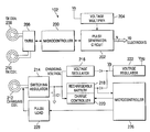
FIG. 2 is a detailed block diagram of the IPG shown in FIG. 1;
FIG. 3 illustrates one embodiment of the pulse loading circuitry;
FIG. 4 is a detailed block diagram of the charging device shown in FIG. 1;
FIG. 5 is a diagram illustrating timing of the switching regulator control signal and pulse load signal generated by the IPG, and the pulse load signals received by the charging device;
FIGS. 6A and 6B are examples of a message/coding table (FIG. 6A) and a protocol and bit timing diagram (FIG. 6B) that may be used in accordance with the present invention; and
FIG. 7 illustrates a stimulation system in accordance with the present invention.
DETAILED DESCRIPTION
The general principles of the present invention is described with respect to an implantable pulse generator (IPG) for generating electrical stimulation for application to a desired area of a body, such as a spinal cord stimulation (SCS) system. It will be understood that the present invention is not limited to an IPG for use in an SCS system, but has broad applicability, including but not limited to different types of implantable devices such as spinal and neural stimulators and sensors, deep brain stimulators, cochlear stimulators, drug delivery systems, muscle tissue stimulators, and the like, including sensors and sensing systems. The present invention is further applicable in systems powered by a replenishable power source wherein the power source is replenished using a recharging signal transmitted wirelessly from a charging device.
Now referring to FIG. 1, there is shown a stimulation system 100 (generally, reference numeral 100) having an implantable pulse generator (IPG) 102, an external communication device 104 (sometimes referred to as an external programming device) and an external charging device 108. The external communication device 104 communicates with the IPG 102 via a wireless communications link 106 and provides functionality and control mechanism to program and control the operating characteristics of the IPG 102, and for other communications between the IPG 102 and device 104. The external charging device 108 transmits a charging signal that is received by IPG 102 via a wireless link 110 and is utilized to recharge a replenishable power source within the IPG 102. The IPG 102 provides electrical pulses or stimulation to a plurality of electrodes or electrode arrays (via a lead extension or lead body) for application at the desired location.
It will be understood by those skilled in the art that the external communications device 104 and the external charging device 108 may be combined into a single device.
Now referring to FIG. 2, a microcontroller 200 and a pulse generator circuit 202 function to program, control and generate electrical signals (stimulation) output to a desired location (via the electrodes). The pulse generator circuit 202 generates a plurality electrical signals for output (i.e., “pulse generator outputs” or “outputs”). The microcontroller 200 generally includes a processor and memory (not specifically shown) and may further be constructed using any hardware, firmware and/or software, or combinations thereof, to provide the functionality described herein. A voltage multiplier 204 generates step-up and/or step-down voltages from a voltage supply Vb for supplying power to the pulse generator circuit 202. The microcontroller 200 and circuit 202 are shown as separate elements, but their functionality may also be provided by a single element (or multiple elements). Further, the pulse generator circuit 202 and microcontroller 200 may include various elements of hardware and/or software.
The microcontroller 200 receives/transmits data and other control signals from/to the external communications device 104 using a transceiver 206 and transmit and receive antenna elements 208, 210. The antenna elements 208, 210 may be one element or separate elements, and may further be constructed of various materials and configurations sufficient to provide the functionality of an antenna element to receive/transmit wireless signals. In one embodiment, the antenna elements are in the form of coils.
A switching regulator 214 receives energy contained with a charging signal received through a charging coil or antenna 212. The received energy is received inductively through the charging coil 212 from the external charging device 108 (FIG. 1) and utilized to recharge a replenishable power source 218 (e.g. rechargeable battery). The charging signal (from the external charging device), and in one embodiment is an RF signal of 2 Mhz, generates a corresponding signal within the charging coil 212. The received signal is rectified by a rectification circuit (not shown, and in one embodiment the rectification circuit includes a full wave bridge rectifier, series capacitor (for filtering) and an optional fuse for safety purposes) and output as an unregulated charging voltage supply. The output of the rectification circuit is input to the switching regulator 214 and coupled to a load pulsing circuit 228. The load pulsing circuit 228 provides a selectively switchable load for increasing the load on the charging coil 212, and is described in more detail further below.
The switching regulator 214 functions to generate a regulated charging voltage for input to the rechargeable battery 218 (to provide power for recharging) and a voltage regulator 216. A capacitor C1 is coupled to the output (regulated charging voltage) of the switching regulator 214 to hold up, or maintain its voltage level during short interruptions of the charging coupling occurring during a pulse loading communications window (as will be described more fully below). The voltage regulator 216 generates and outputs a regulated voltage which is coupled to a diode, as shown in FIG. 2. The rechargeable battery 218 is also coupled to a diode (as shown), and both diodes are coupled to a node for providing the voltage supply Vb which provides power (Vb) to other circuitry in the IPG 102. Such power configuration functions to allow the voltage source for the Vb node to be either the voltage supply from the linear regulator 216 or the rechargeable battery 218, whichever is greater. In normal operation, the voltage source for the Vb node will be the rechargeable battery 218, and during a charging session, it will be from the charging voltage (via the regulator 216). In other words, when sufficient energy is supplied by the switching regulator 214 (charging energy) to generate the regulated voltage higher than the battery voltage, this regulated voltage from the regulator 216 is used to supplant the battery voltage for powering downstream circuitry. A second voltage regulator 222 regulates the voltage Vb to generate another regulated voltage Vreg for use with circuitry requiring a lower voltage supply.
In one example embodiment, the unregulated charging voltage is about 12 volts or greater, while the regulated charging voltage output from the switching regulator 214 is about 6 volts. The output of the voltage regulator 216 is about 4.2 volts while the battery voltage is about 4 volts. With the voltage drop across the diodes, the node Vb will generally be between about 4 and 4.2 volts minus a diode voltage drop. The voltage supply Vreg can be on the order 3.3 to 2.5 volts, as desired.
The IPG 102 includes a microcontroller 226 that initiates and controls communication to the external charging device via a pulse loading communication technique in conjunction with the pulse loading circuit 228. The microcontroller further enables, disables and controls charging of the replenishable power source 218 via a charge controller 220, and monitors status of the charging operation (e.g. enable charger, charging signal present, charging current, charging voltage, etc.). As will be appreciated, the microcontroller 226 generally includes a processor and memory (not specifically shown) and may further be constructed using any hardware, firmware and/or software, or combinations thereof, to provide the functionality described herein. In another embodiment, the microcontroller 200 and the microcontroller 226 may be combined into a single microcontroller or processor.
The charge controller 220 is coupled to the replenishable power source 218 and the microcontroller 226 and is operable to control the charging of the replenishable power source 218. On one embodiment, charging occurs at a constant current until the replenishable power source 218 reaches a target voltage. Thereafter, the charging switches to constant voltage control while the current into the replenishable power source 218 decreases as it continues to charge.
The microcontroller 226 monitors the voltage of the replenishable power source 218 and charging voltages, and is further operable to detect various voltage levels (e.g., low battery, dead battery, etc.). When the voltage(s) reach certain levels, the IPG 102 (and/or other circuitry) is signaled and may go into various modes, such as a sleep mode when the voltage falls below a predetermined level. This voltage monitoring may also be accomplished using other element(s) (not shown) in addition to, or in lieu of, the microcontroller 226.
It is desirable to transmit error or status information (e.g., charging status and voltage, battery voltage levels, temperature overheat, overcurrent, and other operational parameters, etc.) during a recharging session from the IPG 102 to an external device. In prior art systems, such communication is accomplished using a wireless transceiver, similar to the transceiver 206 (FIG. 2) of the present invention, when communication is established with the external communications device 104. However, as mentioned above, the RF recharging energy present during a recharging session is substantial and may interfere with the other communications path between an implantable device and the external communications device. As such, the present invention provides a method and means for communication from the IPG 102 to the external charging device during a recharging session (or cycle). The present invention provides a pulse loading communications technique that minimizes corruption of data transmitted from the IPG 102. One embodiment of the present invention disables the switching regulation in the IPG 102 for a short period of time (to provide a pulse loading communications window) and further utilizes a communications protocol that reduces the likelihood that noise or switching regulation effects will be misinterpreted as transmitted data.
Now referring to FIG. 3, there is shown the switching regulator 214, the microcontroller 226, and one embodiment of the pulse loading circuit 228. The switching regulator 214 operates at a switching frequency (F switch) during a recharging cycle. In one embodiment, circuitry (not shown) is provided that automatically changes the switching frequency to maintain the regulated voltage and an RC time constant circuit (or other circuit) operates to maintain the switching frequency below a particular frequency (as described in more detail herein). In another embodiment, the microcontroller 226 may increase or decrease the switching frequency (switching frequency control signal) depending on the value of the output voltage of the regulator 214 (VSENSE). In addition, an on/off control signal operates to enable/disable operation of the switching regulator 214. During a communications transmission period when pulse loading communications are operable, the switching regulator 214 is disabled.
The pulse loading circuit 228 is coupled to the charging coil to selectively increase the load on the charging coil 212. The pulse loading circuit 228 includes a resistive element R1 and a transistor switch T1, as shown. Other configurations and elements are possible. The pulse loading signal and the pulse loading circuit 228 are used to pulse load the charging coil 212.
Pulse loading effectively increases the current load on the coil 212 which is detectable at the external charging device 108, thus providing a mechanism to effectively communicate to the external charging device 108. Therefore, the coil 212 that is used to receive recharging energy is also used to send messages back to the charging device 108. In addition, because the energy “taken out” of the coil 212 during pulse loading is charging energy, and because the circuitry utilized in the IPG 102 to perform the load pulsing communications uses the charging energy and does not actively transmit energy (which would occur if the transceiver 206 were used), no energy from the replenishable power source 218 is used.
As will be appreciated, during the recharging cycle, the operation of the switching regulator 214 effectively pulse loads the coil 212. This occurs because the load on the charging coil 212 is increased/decreased according to the operation of the switching regulator 214. As such, each switching (on/off) of the switching regulator 214 is also detectable at the external charging device 108. To assist the external charging device 108 in recognizing the desired pulse loading, as opposed to pulse loading resulting from the switching regulation, the present invention (1) disables the switching regulator 214 during a predetermined time period during which the “true” data is transmitted, (2) operates the switching regulator 214 (during enabled operation) at a switching frequency Fswitch that is less than the data hit rate of the pulse loading communication, and (3) employs a communication and data message protocol to reduce the likelihood that noise or switching regulation will be interpreted as valid data.
Now referring to FIG. 4, there is illustrated the charging device 108 in accordance with the present invention. The charging device 108 includes a microcontroller 400, a power supply 402, an RF transmitter drive circuit, a transmit coil or antenna 406, a pulse loading detector 408 and an output device 410.
The power supply 402 provides power to the various elements of the charging device 404 and may include one or more voltage regulators, and further may receive power from an external power supply (AC or DC). The microcontroller 400 functions to control the charging operation, monitor and detect data received by the charging device 108 via pulse loading, and control and output various indicators for recognition by a user. As will be appreciated, the microcontroller 400 generally includes a processor and memory (not specifically shown) and may further be constructed using any hardware, firmware and/or software, or combinations thereof, to provide the functionality described herein. The microcontroller further includes a digital signal processor (or other circuitry, firmware, and/or software) operable for detecting (or differentiating) pulse loading communications from pulse loading resulting from noise or switching regulation operation in the implantable device 102. One way of detecting or differentiating between the two pulse loading detections is to measure pulse widths and/or frequency of received signals. In one embodiment, the frequency of operation of the switching regulation is maintained at a frequency that is less than the frequency of the data bit rate utilized for the actual data communications. In another embodiment, or in addition to the above, a novel communication protocol may be used. Such a protocol is described more fully below.
The transmitter drive circuit 404 includes driver circuitry for transmitting a charging signal to the transmit coil 406 for transmission. Thus, the charging device 108 transmits RF energy to provide power to another device (e.g., to charge a battery). The transmitter drive circuit 404 may optionally include a current limiting device (not shown) to limit the current supplied to the circuit 404, and thus limit the amount of RF energy output.
The pulse loading detector 408 detects pulse loading, which occurs when a load that is receiving the RF energy transmitted by the charging device 108 is changed substantially (i.e., load switched in/out). The detector 408 may optionally include circuitry providing a filtering function to assist in properly detecting pulse loading.
The output device 410 provides visible and/or audible outputs controlled by the microcontroller 400 responsive to data received via the pulse loading. The output device 410 may include different color LEDs, audible indicators operable to provide different tones, and the like, or any other output mechanism to provide an indicator to a user.
The general operation of the system of the present invention will now be described. During a recharging cycle, the IPG 102 receives energy (transmitted from the charging device 108) at the charging coil 212. The received energy is converted to an unregulated voltage and input to a switching regulator (operating at a switching frequency Fswitch) to generate a regulated voltage. The regulated voltage thereafter provides power to operate some or all of the circuitry in the IPG 102 and charge the replenishable power source 218 (e.g. rechargeable battery).
In order for the IPG 102 to communicate information (such as battery, charging and status information, and any other desired information) to the external charging device 108 during the recharge cycle, the IPG 102 employs intentional pulse loading of the charging coil 212 to relay data bits back to the external charging device 108. Switching regulation occurring in the IPG 102 is disabled for a predetermined period of time (pulse loading communications window) to allow pulse loading communications to occur. Pulse loading communication is accomplished by selectively switching in and out a load on the charging coil 212 which corresponds to logic ones and zeros (data bits). The present invention provides that pulse loading (e.g., data bit rate) occurs at a frequency that is greater than the switching regulation frequency. Optionally, data is transmitted using a predetermined coding scheme to reduce the likelihood of errors during detection (or falsely detecting a data message during operation of the switching regulator or caused by other noise).
Pulse loading within the IPG 102 (i.e., the charging coil 212) generates corresponding and detectable signal(s) in the transmit coil 406 of the external charging device 108. Detected pulses are signal processed to detect/differentiate received “true” data from pulses resulting from switching regulation or noise. Upon detection and decoding of the data message(s), the external charging device 108 outputs corresponding indicia (such as LEDs, other display means, and/or audible signals) for communication to a user. As will be appreciated, the external charging device 108 may also perform other functions in response to the received data communication.
Now referring to FIG. 5, there is shown a timing diagram illustrating aspects of the present invention. The timing diagram illustrates various events occurring during a recharging cycle, and more specifically identify (1) the switching regulator on/off control signal (to enable/disable operation), (2) pulse loading signal (output from the microcontroller 226 and controlling the pulse loading circuit 228), and (3) the signal output from the pulse load detector 408 in the external charging device 108.
During a time T1, the switching regulator 214 is active, data pulse loading is inactive, and the signal output from the pulse detector 408 shows pulses being detected (due to active switching regulation in the IPG 102, e.g., charging the battery), as shown. During time period T2 (pulse loading communication window), the switching regulator 214 is deactivated, data pulse loading becomes active, and the signal output from the pulse detector 408 shows that the data pulse loading is correspondingly detected, as shown. During time T3, the switching regulator 214 is again active, data pulse loading is inactive, and the signal output from the pulse detector 408 shows pulses being detected (due to the active switching regulation).
In one embodiment of the present invention, the switching regulator 214 is operated at a frequency Fswitch that is less than the data bit rate (or frequency) of the pulse loading data. As will be appreciated, the magnitude of the difference in these frequencies will depend on the signal processing capabilities and functionality of the external charging device 108. Moreover, it will be understood that different detection methods and means may be utilized to detect or differentiate the received data pulses from received pulses resulting from switching regulation or other noise (“unwanted” pulse loading detection). Using pulse width and/or frequency delineation is one method in accordance with the present invention.
To further reduce the likelihood of misinterpretation caused by switching regulation or other noise, a communications protocol, data coding and message scheme is provided. Typical data messages may include data for commands, status, state and errors. Now referring to FIGS. 6A and 6B, there is illustrated one embodiment of a message/coding table (FIG. 6A) and a protocol and bit timing diagram (FIG. 6B) in accordance with the present invention.
In one embodiment of the present invention, a data message includes a start sequence (or bits), code, and stop bit (or sequence). In the example, the start sequence includes a 00101 sequence of bits, the code includes four data bits (representing codes 0 to 15; EOLH and EOLL refer to the contents of high and low nibbles of an end-of-life (EOL) register in the IPG 102), and the stop bit includes a single logic zero data bit. The data bit width is shown as 122 microseconds, corresponding to a data bit rate or frequency of around 8 KHz or higher. Other data bit rates or frequencies may be used. In one embodiment of the present invention, the data bit rate (or frequency) is greater than switching frequency Fswitch of the switching regulator 214. As will be appreciated, other data message structures (start sequence, code, stop sequence, etc.) may also be utilized. As described, one embodiment of the start sequence is a 00101 start sequence that enhances the probability of proper decoding of messages or codes. Other sequences or bit(s) may be used.
The table shown in FIG. 6A illustrates examples of codes and their associated messages. Other and different messages and coding techniques may be used, in addition to those shown. A corresponding message is determined based upon three codes (transmitted separately in data messages). For example, three separate data messages (as shown in FIG. 6B) each including a code are used to correspond or represent a given message. The external charging device 108 includes functionality to decode and interpret the separate data messages and messages/information corresponding thereto. The resulting information is then transmitted to the user by means of the output device 410. Such messages/information may relate to charging, faults, status, errors, and/or commands, or combinations thereof, and the like.
Accordingly, the general operation of transmitting a message pulse loading communication occurs as follows: The IPG 102 disables the switching regulator 214 to provide pulse communications window. A data message (similar to that shown in FIG. 6B, with a code) is transmitted using the pulse loading technique during the window, and the switching regulator is enabled. This operation is then repeated a second and third time, with a second code and third code respectively. The charging device 108 receives, detects, and decodes the data messages to determine the information transmitted. Based upon this, the charging device 108 outputs an indicator or indicators to a user notifying the user of the message or condition.
Other data bit timing, protocol and coding schemes are contemplated by the present invention. Such may be used to increase data integrity and correctly decode the transmitted message/information. Optionally, the data messages may be transmitted/received multiple times before a message is deemed valid for communication to the user.
It will be understood that the present invention is not limited to communications and operation only during a recharge cycle for an IPG, but may also be utilized during power transfer to (and operation of) an externally-powered IPG. Communications from the IPG 102 using a wireless power link that is providing power to the IPG 102 from an external device (104 or 108) are contemplated by the present invention. Moreover, the present invention is not limited to implantable devices (and “external” devices), but may also be practiced in other devices that receive power wirelessly (whether or not one device is implanted).
With reference to FIG. 7, there is shown a stimulation system 700 in accordance with the present invention. The stimulation system 700 generates and applies a stimulus to a tissue or to a certain location of a body. In general terms, the system 700 includes an IPG 710, in accordance with that described herein, that provides a stimulation or energy source and a lead 10 for application of the stimulus. The lead 10 shown in FIG. 7 is described below.
The lead 10 includes a distal end 14 and a proximal end 16. The lead 10 includes a lead body 12 that extends from the distal end 14 to the proximal end 16. The distal end 14 of the lead 10 is shown including four electrodes 18. The proximal end 16 of the lead 10 includes four contact electrodes (or ring electrodes) (not shown) that form a lead connector. The lead 10 generally includes one or more conductors (not shown) extending a substantial portion of the lead 10 to electrically connect the contact electrodes to respective electrodes 18. An optional lumen (not shown) may extend through the lead 10 and may be used for different purposes, including the delivery of chemicals or drugs.
As will be appreciated, any number of conductors and electrodes may be utilized, as desired. For purposes of illustration only, the lead 10 is shown with four electrodes. In addition, other types, configurations and shapes of electrodes (and lead connectors) as known to those skilled in the art may be used, as desired.
Typically, the lead body 12 is a structure having a round cross-section. Alternatively, the cross-section of the lead body 12 may be configured in any number of cross-sectional shapes appropriate for the specific application. The following description generally refers to a round cross-sectional shape for the lead body 12 for illustrative purposes only. The lead body 12 generally includes a lead body insulator configured to insulate the conductors and present a biocompatible external surface to the body tissue.
The lead body insulator is formed of insulating material typically selected based upon biocompatibility, biostability and durability for the particular application. The insulator material may be silicone, polyurethane, polyethylene, polyamide, polyvinylchloride, PTFT, EFTE, or other suitable materials known to those skilled in the art. Alloys or blends of these materials may also be formulated to control the relative flexibility, torqueability, and pushability of the lead. Depending on the particular application, the diameter of the lead body 12 may be any size, though a smaller size is more desirable for neurological and myocardial mapping/ablation leads and neuromodulation and stimulation leads.
The conductors (not shown) may take the form of solid wires, drawn-filled-tube (DFT), drawn-brazed-strand (DBS), stranded wires or cables, ribbon conductors, or other forms known or recognized to those skilled in the art. The composition of the conductors may include aluminum, stainless steel, MP35N, platinum, gold, silver, copper, vanadium, alloys, or other conductive materials or metals known to those of ordinary skill in the art. The number, size, and composition of the conductors will depend on the particular application for the lead 10, as well as the number of electrodes.
The conductors may be configured along the lead body 12 in a straight orientation or spirally or helically wound about the optional lumen or center of the lead body 12. The conductors are typically insulated from the optional lumen, from each other, and from the external surface of the lead 10 by insulative material. The insulative material may be of a single composition, or multiple layers of the same or different materials.
In one embodiment, the lead 10 is generally configured to transmit one or more electrical signals from a source for application at, or proximate to, a spinal nerve or peripheral nerve, or other tissue.
The electrodes are typically made of a conductive material such as platinum, gold, silver, platinum-iridium, stainless steel, MS35N, or other conductive materials, metals or alloys known to those skilled in the art. The size of the electrodes is generally chosen based upon the desired application.
As shown in FIG. 7, the stimulation system 700 includes the lead 10 that is coupled to the IPG 710.
In one embodiment, the IPG 710 may include a self-contained implantable pulse generator (SCIPG) or externally-powered implantable pulse generator (EPIPG). As used herein, an SCIPG is an IPG having an implanted power source, such as a long-lasting or replenishable power source (e.g. rechargeable battery). An EPIPG is an IPG that does not include a long-lasting or replenishable power source and that receives its operating power from an external power transmitter, preferably in the form of a wireless signal (RF, inductive, etc.). As is known in the art, an IPG is capable of being implanted within the body (not shown) that receives electrical stimulation from the IPG 710.
An external communications device 720 (the same as or similar to the device 104, or programmer/controller) may be provided to control and/or program the IPG 710 via a communications link 730 (same as or similar to the communications link 106). When in the form of an SCIPG with a replenishable power source, the device 720 may also provide power to the IPG 710 through an integrated or separate charging device (the same as or similar to charging device 108). When in the form of an EPIPG, the device 720 usually provides both power and control communications to the IPG 710. A separate controller 740 may be provided which controls/programs the device 720. In some embodiments, the controller 740, or collectively the device 720 and controller 740, are referred to as an external patient controller/programmer (EPP).
As shown in FIG. 7, the stimulation system 700 includes the lead 10 that is coupled to the IPG 710. The IPG 710 is the same as or similar to the IPG 102. Communication/power signals are represented in FIG. 7 by the wireless link symbol 730 (the same as or similar to links 106 and 110 in FIG. 1). The device 720 and the controller 740 are located external to the body that is to receive electrical stimulation from the IPG 710. A user of the IPG 710 may use the device 720 and/or controller 740 to provide control signals for the operation of the IPG 710. The controller 740 provides control signals to the device 720. The device 720 transmits the control signals (and optionally power) to a receiver in the IPG 710, and the IPG 710 responds to the control signals to vary the signal parameters of the electrical signals that are transmitted through lead to the stimulation site.
As will be appreciated, the contact electrodes are not visible in FIG. 7 because the contact electrodes are situated within a receptacle (not shown) of the IPG 710. The contact electrodes electrically connect to a pulse generator circuit within the IPG 710. The IPG 710 generates and sends electrical signals via the lead 10 to the electrodes 18. Understandably, the electrodes 18 are located at a stimulation site (not shown) within the body that is to receive electrical stimulation from the electrical signals. A stimulation site may be, for example, adjacent to one or more nerves in the central nervous system (e.g., spinal cord). The IPG 710 is capable of controlling the electrical signals by varying signal parameters (e.g., intensity, duration, frequency) in response to control signals that are provided to the IPG 710.
It may be advantageous to set forth definitions of certain words and phrases that may be used within this patent document: the terms “include” and “comprise,” as well as derivatives thereof, mean inclusion without limitation; the term “or,” is inclusive, meaning and/or; the phrases “associated with” and “associated therewith,” as well as derivatives thereof, may mean to include, be included within, interconnect with, contain, be contained within, connect to or with, couple to or with, be communicable with, cooperate with, interleave, juxtapose, be proximate to, be bound to or with, have, have a property of, or the like; and if the term “controller” is utilized herein, it means any device, system or part thereof that controls at least one operation, such a device may be implemented in hardware, firmware or software, or some combination of at least two of the same. It should be noted that the functionality associated with any particular controller may be centralized or distributed, whether locally or remotely. The term “couple” or “connect” refers to any direct or indirect connection between two or more components, unless specifically noted that a direct coupling or direct connection is present.
Although the present invention and its advantages have been described in the foregoing detailed description and illustrated in the accompanying drawings, it will be understood by those skilled in the art that the invention is not limited to the embodiment(s) disclosed but is capable of numerous rearrangements, substitutions and modifications without departing from the spirit and scope of the invention as defined by the appended claims.
Although the present invention and its advantages have been described in detail, it should be understood that various changes, substitutions and alterations can be made herein without departing from the spirit and scope of the invention as defined by the appended claims. Moreover, the scope of the present application is not intended to be limited to the particular embodiments of the process, machine, manufacture, composition of matter, means, methods and steps described in the specification. As one of ordinary skill in the art will readily appreciate from the disclosure of the present invention, processes, machines, manufacture, compositions of matter, means, methods, or steps, presently existing or later to be developed that perform substantially the same function or achieve substantially the same result as the corresponding embodiments described herein may be utilized according to the present invention. Accordingly, the appended claims are intended to include within their scope such processes, machines, manufacture, compositions of matter, means, methods, or steps.

Claims (10)

1. An implantable medical device, the implantable medical device adapted to receive wireless energy from a charging device, the implantable medical device comprising:
an antenna element operable for receiving wireless energy transmitted from the charging device;
a switching regulator coupled to the antenna element and having circuitry for enabling operation of the switching regulator during a first predetermined time period and for disabling operation of the switching regulator during a second predetermined time period in response to a switching regulator control signal, the switching regulator operable for receiving and regulating the received wireless energy and outputting a regulated voltage;
a rechargeable battery coupled to the switching regulator for receiving current from the switching regulator during the first predetermined time period; and
a pulse loading circuit coupled to the antenna element and operable for receiving one or more pulse loading pulses during the second predetermined time period and pulse loading the antenna element in response to the one or more pulse loading pulses, and wherein the pulse loading the antenna element is operable to transmit data to the charging device.
2. The implantable medical device in accordance with claim 1 wherein the switching regulator operates at a first switching frequency and the data transmitted to the external device has a data bit rate of a second frequency higher than the first switching frequency.
3. The implantable medical device in accordance with claim 1 wherein operation of the switching regulator affects the antenna element sufficient to generate signals detectable in the charging device.
4. The implantable medical device in accordance with claim 1 wherein the pulse loading circuit further comprises:
a switch coupled to the antenna element; and
a resistive element connected to the switch and to a first voltage supply for diverting a current from the antenna element.
5. An implantable pulse generator for generating electrical pulses to stimulation of tissue of a patient, the pulse generator comprising:
a processor for controlling the implantable pulse generator;
pulse generating circuitry for generating electrical pulses for application to tissue of the patient;
an antenna element operable for receiving wireless energy transmitted from an external charging device after the implantable pulse generator is implanted within the body of a patient;
a switching regulator coupled to the antenna element and having circuitry for enabling operation of the switching regulator during a first predetermined time period and for disabling operation of the switching regulator during a second predetermined time period in response to a switching regulator control signal from the processor, the switching regulator operable for receiving and regulating the received wireless energy and outputting a regulated voltage;
a rechargeable battery coupled to the switching regulator for receiving current from the switching regulator during the first predetermined time period; and
a pulse loading circuit coupled to the antenna element for selectively coupling a current load to the antenna element to transmit data to the external charging device according to a data stream from the processor.
6. The implantable medical device in accordance with claim 5 wherein the switching regulator operates at a first switching frequency and the data transmitted to the external device has a data bit rate of a second frequency higher than the first switching frequency.
7. The implantable medical device in accordance with claim 5 wherein operation of the switching regulator affects the antenna element sufficient to generate signals detectable in the charging device.
8. The implantable medical device in accordance with claim 5 wherein the pulse loading circuit further comprises:
a switch coupled to the antenna element; and
a resistive element connected to the switch and to a first voltage supply for diverting a current from the antenna element.
9. The implantable medical device of claim 5, wherein the processor controls an operating frequency of the switching regulator during the first predetermined time period.
10. The implantable medical device of claim 5, wherein the data stream includes start bit sequences before respective data messages.
US11/688,488 2004-04-19 2007-03-20 Implantable device and system and method for wireless communication Active 2027-01-12 US7782190B1 (en)

Priority Applications (1)

Application Number Priority Date Filing Date Title
US11/688,488 US7782190B1 (en) 2004-04-19 2007-03-20 Implantable device and system and method for wireless communication

Applications Claiming Priority (3)

Application Number Priority Date Filing Date Title
US56362204P 2004-04-19 2004-04-19
US11/109,114 US7212110B1 (en) 2004-04-19 2005-04-19 Implantable device and system and method for wireless communication
US11/688,488 US7782190B1 (en) 2004-04-19 2007-03-20 Implantable device and system and method for wireless communication

Related Parent Applications (1)

Application Number Title Priority Date Filing Date
US11/109,114 Continuation US7212110B1 (en) 2004-04-19 2005-04-19 Implantable device and system and method for wireless communication

Publications (1)

Publication Number Publication Date
US7782190B1 true US7782190B1 (en) 2010-08-24

Family

ID=37991461

Family Applications (2)

Application Number Title Priority Date Filing Date
US11/109,114 Expired - Fee Related US7212110B1 (en) 2004-04-19 2005-04-19 Implantable device and system and method for wireless communication
US11/688,488 Active 2027-01-12 US7782190B1 (en) 2004-04-19 2007-03-20 Implantable device and system and method for wireless communication

Family Applications Before (1)

Application Number Title Priority Date Filing Date
US11/109,114 Expired - Fee Related US7212110B1 (en) 2004-04-19 2005-04-19 Implantable device and system and method for wireless communication

Country Status (1)

Country Link
US (2) US7212110B1 (en)

Cited By (32)

* Cited by examiner, † Cited by third party
Publication number Priority date Publication date Assignee Title
US20090062652A1 (en) * 2007-08-31 2009-03-05 Soo Hwan Shin Wirelessly Chargeable And Portable Ultrasonic Diagnostic Device
US20100141051A1 (en) * 2006-05-12 2010-06-10 Christian Vollaire Device for converting an electromagnetic wave into dc voltage
CN102687411A (en) * 2010-01-12 2012-09-19 株式会社巨晶片 Communication system,communication apparatus,and integrated circuit for communication
US8514067B2 (en) 2011-08-16 2013-08-20 Elwha Llc Systematic distillation of status data relating to regimen compliance
US8594806B2 (en) 2010-04-30 2013-11-26 Cyberonics, Inc. Recharging and communication lead for an implantable device
US8639335B2 (en) * 2011-01-28 2014-01-28 Medtronic, Inc. Disabling an implanted medical device with another medical device
US9287040B2 (en) 2012-07-27 2016-03-15 Thoratec Corporation Self-tuning resonant power transfer systems
US9343923B2 (en) 2012-08-23 2016-05-17 Cyberonics, Inc. Implantable medical device with backscatter signal based communication
US20160301238A1 (en) * 2015-04-10 2016-10-13 Intel Corporation Managing presence and long beacon extension pulses
US9583874B2 (en) 2014-10-06 2017-02-28 Thoratec Corporation Multiaxial connector for implantable devices
US9592397B2 (en) 2012-07-27 2017-03-14 Thoratec Corporation Thermal management for implantable wireless power transfer systems
US9680310B2 (en) 2013-03-15 2017-06-13 Thoratec Corporation Integrated implantable TETS housing including fins and coil loops
US9805863B2 (en) 2012-07-27 2017-10-31 Thoratec Corporation Magnetic power transmission utilizing phased transmitter coil arrays and phased receiver coil arrays
US9825471B2 (en) 2012-07-27 2017-11-21 Thoratec Corporation Resonant power transfer systems with protective algorithm
US9855437B2 (en) 2013-11-11 2018-01-02 Tc1 Llc Hinged resonant power transfer coil
US9935498B2 (en) 2012-09-25 2018-04-03 Cyberonics, Inc. Communication efficiency with an implantable medical device using a circulator and a backscatter signal
US10148126B2 (en) 2015-08-31 2018-12-04 Tc1 Llc Wireless energy transfer system and wearables
US10177604B2 (en) 2015-10-07 2019-01-08 Tc1 Llc Resonant power transfer systems having efficiency optimization based on receiver impedance
US10186760B2 (en) 2014-09-22 2019-01-22 Tc1 Llc Antenna designs for communication between a wirelessly powered implant to an external device outside the body
US10251987B2 (en) 2012-07-27 2019-04-09 Tc1 Llc Resonant power transmission coils and systems
US10291067B2 (en) 2012-07-27 2019-05-14 Tc1 Llc Computer modeling for resonant power transfer systems
US10373756B2 (en) 2013-03-15 2019-08-06 Tc1 Llc Malleable TETs coil with improved anatomical fit
US10383990B2 (en) 2012-07-27 2019-08-20 Tc1 Llc Variable capacitor for resonant power transfer systems
US10525181B2 (en) 2012-07-27 2020-01-07 Tc1 Llc Resonant power transfer system and method of estimating system state
US10546105B1 (en) 2016-12-14 2020-01-28 KaBOODL, INC. 3D printer and inventory control and distribution system for 3D designs
US10610692B2 (en) 2014-03-06 2020-04-07 Tc1 Llc Electrical connectors for implantable devices
US10615642B2 (en) 2013-11-11 2020-04-07 Tc1 Llc Resonant power transfer systems with communications
US10695476B2 (en) 2013-11-11 2020-06-30 Tc1 Llc Resonant power transfer systems with communications
US10770923B2 (en) 2018-01-04 2020-09-08 Tc1 Llc Systems and methods for elastic wireless power transmission devices
US10846808B1 (en) 2016-12-14 2020-11-24 Kaboodl, LLC 3D printer and inventory control and distribution system for 3D designs
US10898292B2 (en) 2016-09-21 2021-01-26 Tc1 Llc Systems and methods for locating implanted wireless power transmission devices
US11197990B2 (en) 2017-01-18 2021-12-14 Tc1 Llc Systems and methods for transcutaneous power transfer using microneedles

Families Citing this family (131)

* Cited by examiner, † Cited by third party
Publication number Priority date Publication date Assignee Title
US7444184B2 (en) * 2003-05-11 2008-10-28 Neuro And Cardial Technologies, Llc Method and system for providing therapy for bulimia/eating disorders by providing electrical pulses to vagus nerve(s)
US8024036B2 (en) 2007-03-19 2011-09-20 The Invention Science Fund I, Llc Lumen-traveling biological interface device and method of use
US8092549B2 (en) 2004-09-24 2012-01-10 The Invention Science Fund I, Llc Ciliated stent-like-system
US9801527B2 (en) 2004-04-19 2017-10-31 Gearbox, Llc Lumen-traveling biological interface device
US9011329B2 (en) 2004-04-19 2015-04-21 Searete Llc Lumenally-active device
US7212110B1 (en) * 2004-04-19 2007-05-01 Advanced Neuromodulation Systems, Inc. Implantable device and system and method for wireless communication
US8337482B2 (en) 2004-04-19 2012-12-25 The Invention Science Fund I, Llc System for perfusion management
US8353896B2 (en) 2004-04-19 2013-01-15 The Invention Science Fund I, Llc Controllable release nasal system
US8361013B2 (en) 2004-04-19 2013-01-29 The Invention Science Fund I, Llc Telescoping perfusion management system
US7720546B2 (en) * 2004-09-30 2010-05-18 Codman Neuro Sciences Sárl Dual power supply switching circuitry for use in a closed system
US7545272B2 (en) 2005-02-08 2009-06-09 Therasense, Inc. RF tag on test strips, test strip vials and boxes
US20070149162A1 (en) * 2005-02-24 2007-06-28 Powercast, Llc Pulse transmission method
US8186358B2 (en) * 2005-07-29 2012-05-29 Codman Neuro Sciences Sárl System and method for locating an internal device in a closed system
US9198563B2 (en) 2006-04-12 2015-12-01 The Invention Science Fund I, Llc Temporal control of a lumen traveling device in a body tube tree
US20080058788A1 (en) 2006-04-12 2008-03-06 Searete Llc., A Limited Liability Corporation Of The State Of Delaware Autofluorescent imaging and target ablation
US8163003B2 (en) * 2006-06-16 2012-04-24 The Invention Science Fund I, Llc Active blood vessel sleeve methods and systems
US20080103572A1 (en) 2006-10-31 2008-05-01 Medtronic, Inc. Implantable medical lead with threaded fixation
US20080177353A1 (en) * 2006-12-28 2008-07-24 Takashi Hirota Cochlear implant device, extracorporeal sound collector, and cochlear implant system having the same
JP2011500203A (en) * 2007-10-16 2011-01-06 ミルックス・ホールディング・エスエイ Method and apparatus for supplying energy to a medical device
US9089707B2 (en) 2008-07-02 2015-07-28 The Board Of Regents, The University Of Texas System Systems, methods and devices for paired plasticity
US8457757B2 (en) * 2007-11-26 2013-06-04 Micro Transponder, Inc. Implantable transponder systems and methods
EP2071497A1 (en) * 2007-12-10 2009-06-17 Gemalto SA Contactless battery charger method and device
US20090184825A1 (en) * 2008-01-23 2009-07-23 General Electric Company RFID Transponder Used for Instrument Identification in an Electromagnetic Tracking System
EP2258033A2 (en) 2008-02-22 2010-12-08 Access Business Group International LLC Inductive power supply system with battery type detection
TWI364895B (en) * 2008-06-09 2012-05-21 Univ Nat Taipei Technology Wireless power transmitting apparatus
US20090322285A1 (en) * 2008-06-25 2009-12-31 Nokia Corporation Method and Apparatus for Wireless Charging Using a Multi-Band Antenna
US8364279B2 (en) 2008-09-25 2013-01-29 Boston Scientific Neuromodulation Corporation Electrical stimulation leads having RF compatibility and methods of use and manufacture
JP6029827B2 (en) * 2008-09-25 2016-11-24 コーニンクレッカ フィリップス エヌ ヴェKoninklijke Philips N.V. Device comprising a wireless communication module
ES2959487T3 (en) * 2008-10-10 2024-02-26 Implantica Patent Ltd A procedure to control the wireless transmission of power to a medical device
US8929957B2 (en) 2008-11-21 2015-01-06 Qualcomm Incorporated Reduced jamming between receivers and wireless power transmitters
US9370664B2 (en) 2009-01-15 2016-06-21 Boston Scientific Neuromodulation Corporation Signaling error conditions in an implantable medical device system using simple charging coil telemetry
US20100249552A1 (en) * 2009-03-31 2010-09-30 Nellcor Puritan Bennett Llc System And Method For Wirelessly Powering Medical Devices
US20100305663A1 (en) * 2009-06-02 2010-12-02 Boston Scientific Neuromodulation Corporation Implantable medical device system having short range communication link between an external controller and an external charger
US8577474B2 (en) * 2009-11-11 2013-11-05 Boston Scientific Neuromodulation Corporation Minimizing interference between charging and telemetry coils in an implantable medical device
US8457756B2 (en) 2009-11-11 2013-06-04 Boston Scientific Neuromodulation Corporation Using the case of an implantable medical device to broaden communication bandwidth
US20110221387A1 (en) * 2010-03-09 2011-09-15 Robert Louis Steigerwald System and method for charging an energy storage system for an electric or hybrid-electric vehicle
US20120089203A1 (en) 2010-10-12 2012-04-12 Advanced Neuromodulation Systems, Inc. Electrical connections for use in implantable medical devices
US9132276B2 (en) * 2010-12-10 2015-09-15 Cochlear Limited Portable power charging of implantable medical devices
KR101662513B1 (en) * 2011-05-04 2016-10-05 현대자동차주식회사 Method for prevent frequency interference of wireless power transmission
US9011510B2 (en) 2011-05-09 2015-04-21 The Invention Science Fund I, Llc Method, device and system for modulating an activity of brown adipose tissue in a vertebrate subject
US9238133B2 (en) 2011-05-09 2016-01-19 The Invention Science Fund I, Llc Method, device and system for modulating an activity of brown adipose tissue in a vertebrate subject
US9393433B2 (en) 2011-07-20 2016-07-19 Boston Scientific Neuromodulation Corporation Battery management for an implantable medical device
US20130158638A1 (en) 2011-11-11 2013-06-20 Advanced Neuromodulation Systems, Inc. Stimulation lead and method of fabrication
US8867776B2 (en) 2012-01-09 2014-10-21 Imation Corp. Audio speaker frame for multimedia device
WO2013106407A1 (en) * 2012-01-09 2013-07-18 Imation Corp. Wireless audio player and speaker system
US9071906B2 (en) 2012-01-09 2015-06-30 Imation Corp. Wireless audio player and speaker system
EP2891239B1 (en) 2012-08-31 2019-02-13 The Alfred E. Mann Foundation for Scientific Research Feedback controlled coil driver for inductive power transfer
US9462958B2 (en) * 2013-03-15 2016-10-11 Flint Hills Scientific, Llc Method and system for using tri-modal sensor
AU2014232252B2 (en) 2013-03-15 2018-01-18 Alfred E. Mann Foundation For Scientific Research Current sensing multiple output current stimulators with fast turn on time
AU2014232255B2 (en) 2013-03-15 2017-08-31 Alfred E. Mann Foundation For Scientific Research High voltage monitoring successive approximation analog to digital converter
CN105658276B (en) 2013-05-03 2018-10-02 艾尔弗雷德·E·曼科学研究基金会 Implantation material recharger is shaken hands system and method
WO2014179811A1 (en) 2013-05-03 2014-11-06 Alfred E. Mann Foundation For Scientific Research Multi-branch stimulation electrode for subcutaneous field stimulation
JP6702856B2 (en) 2013-05-03 2020-06-03 アルフレッド イー. マン ファウンデーション フォー サイエンティフィック リサーチ Reliable wire welding for embedded devices
US9780596B2 (en) 2013-07-29 2017-10-03 Alfred E. Mann Foundation For Scientific Research Microprocessor controlled class E driver
EP3028365A1 (en) 2013-07-29 2016-06-08 Alfred E. Mann Foundation for Scientific Research Implant charging field control through radio link
AU2014296322B2 (en) 2013-07-29 2020-01-16 Alfred E. Mann Foundation For Scientific Research High efficiency magnetic link for implantable devices
EP2835913A1 (en) * 2013-08-06 2015-02-11 Hyundai Motor Company Wireless power transmission method for preventing frequency interference and system therefor
US9333351B2 (en) 2013-12-16 2016-05-10 Pacesetter, Inc. Neurostimulation method and system to treat apnea
US9345883B2 (en) 2014-02-14 2016-05-24 Boston Scientific Neuromodulation Corporation Rechargeable-battery implantable medical device having a primary battery active during a rechargeable-battery undervoltage condition
US9999772B2 (en) 2014-04-03 2018-06-19 Pacesetter, Inc. Systems and method for deep brain stimulation therapy
US9445264B2 (en) 2014-05-22 2016-09-13 Pacesetter, Inc. System and method for establishing a secured connection between an implantable medical device and an external device
EP3643355A1 (en) 2014-06-03 2020-04-29 Pop Test Abuse Deterrent Technology LLC Drug device configured for wireless communication
WO2016018867A1 (en) * 2014-07-30 2016-02-04 General Electric Company Wireless charging system for wirelessly charging ultrasound imaging system
EP3180071B1 (en) 2014-08-15 2021-09-22 Axonics, Inc. External pulse generator device and associated system for trial nerve stimulation
US9802038B2 (en) 2014-08-15 2017-10-31 Axonics Modulation Technologies, Inc. Implantable lead affixation structure for nerve stimulation to alleviate bladder dysfunction and other indication
US10682521B2 (en) 2014-08-15 2020-06-16 Axonics Modulation Technologies, Inc. Attachment devices and associated methods of use with a nerve stimulation charging device
CA2958199C (en) 2014-08-15 2023-03-07 Axonics Modulation Technologies, Inc. Electromyographic lead positioning and stimulation titration in a nerve stimulation system for treatment of overactive bladder
JP6878269B2 (en) 2014-08-15 2021-05-26 アクソニクス モジュレーション テクノロジーズ インコーポレイテッド Systems and Methods for Nerve Stimulation Electrode Configuration Based on Nerve Positioning
WO2016025915A1 (en) 2014-08-15 2016-02-18 Axonics Modulation Technologies, Inc. Integrated electromyographic clinician programmer for use with an implantable neurostimulator
US9610448B2 (en) 2014-11-12 2017-04-04 Pacesetter, Inc. System and method to control a non-paresthesia stimulation based on sensory action potentials
US9492660B2 (en) 2014-12-09 2016-11-15 Pacesetter, Inc. Implantable neurostimulation systems and methods thereof
CN107427683B (en) 2015-01-09 2019-06-21 艾克索尼克斯调制技术股份有限公司 For can plant the improvement antenna and application method of nerve stimulator
CN107427685B (en) 2015-01-09 2021-09-21 艾克索尼克斯股份有限公司 Attachment devices for use with neurostimulation charging devices and associated methods
EP3242712B1 (en) 2015-01-09 2019-04-10 Axonics Modulation Technologies, Inc. Patient remote and associated methods of use with a nerve stimulation system
US10456073B2 (en) 2015-06-09 2019-10-29 The Governing Council Of The University Of Toronto System, method and apparatus for rapid brief feedback intracerebral stimulation based on real-time desynchronization
CA2988789A1 (en) 2015-06-09 2016-12-15 The Governing Council Of The University Of Toronto Systems, methods and apparatuses for in situ electrochemical imaging
US10583294B2 (en) 2015-07-02 2020-03-10 Dirk De Ridder Methods and apparatus for sensing cross-frequency coupling and neuromodulation
JP6946261B2 (en) 2015-07-10 2021-10-06 アクソニクス インコーポレイテッド Implantable nerve stimulators and methods with internal electronics without ASICs
US9492667B1 (en) 2015-09-03 2016-11-15 Pacesetter, Inc. Systems and methods for closed loop neurostimulation
US11036294B2 (en) 2015-10-07 2021-06-15 The Governing Council Of The University Of Toronto Wireless power and data transmission system for wearable and implantable devices
US10124177B2 (en) 2015-11-03 2018-11-13 Pacesetter, Inc. Systems and methods for programming implantable devices
US9981131B2 (en) 2015-11-19 2018-05-29 Pacesetter, Inc. Systems and methods for determining spinal cord stimulation parameters based on patient feedback
US9974966B2 (en) 2015-12-15 2018-05-22 Pacesetter, Inc. Systems and methods for manufacturing header subassembly
US9517338B1 (en) 2016-01-19 2016-12-13 Axonics Modulation Technologies, Inc. Multichannel clip device and methods of use
US10195423B2 (en) 2016-01-19 2019-02-05 Axonics Modulation Technologies, Inc. Multichannel clip device and methods of use
JP6876363B2 (en) 2016-01-29 2021-05-26 アクソニクス モジュレーション テクノロジーズ インコーポレイテッド Methods and systems for frequency adjustment that optimize the charging of implantable neurostimulators
WO2017139784A1 (en) 2016-02-12 2017-08-17 Axonics Modulation Technologies, Inc. External pulse generator device and associated methods for trial nerve stimulation
US10953230B2 (en) 2016-07-20 2021-03-23 The Governing Council Of The University Of Toronto Neurostimulator and method for delivering a stimulation in response to a predicted or detected neurophysiological condition
US11369788B2 (en) 2017-06-23 2022-06-28 Advanced Neuromodulation Systems, Inc. Stimulation lead and method including a multi-dimensional electrode array
US11311719B2 (en) 2017-06-23 2022-04-26 Advanced Neuormodulation Systems, Inc. Stimulation lead and method including a multi-dimensional electrode array
EP3641874B1 (en) 2017-06-23 2021-05-12 Pacesetter, Inc. Stimulation lead and method including a multi-dimensional electrode array
CN107376121B (en) * 2017-09-01 2020-11-13 清华大学 Percutaneous wireless charging system and method with adaptive transmission power adjustment function
US10792502B2 (en) 2017-11-08 2020-10-06 Advanced Neuromodulation Systems, Inc. Method and system for adjusting a neurostimulation therapy
US20190134382A1 (en) 2017-11-08 2019-05-09 Pacesetter, Inc. Method and system for adjusting stimulation therapy
CN111741789A (en) 2018-02-22 2020-10-02 艾克索尼克斯调制技术股份有限公司 Neural stimulation leads for testing neural stimulation and methods of use
US11063418B2 (en) * 2018-04-19 2021-07-13 Verily Life Sciences Llc Systems and methods for overcurrent protection for wireless power receivers
US11172857B2 (en) 2018-07-11 2021-11-16 The Governing Council Of The University Of Toronto System, system architecture, and method for neural cross-frequency coupling analysis
US10967190B2 (en) 2018-11-02 2021-04-06 Advanced Neuromodulation Systems, Inc. Methods of operating a system for management of implantable medical devices (IMDs) using reconciliation operations and revocation data
US11173311B2 (en) 2018-11-02 2021-11-16 Advanced Neuromodulation Systems, Inc. Methods for programming an implantable medical device and related systems and devices
US11083900B2 (en) 2018-11-02 2021-08-10 Advanced Neuromodulation Systems, Inc. Methods for operating a system for management of implantable medical devices and related systems
US11090496B2 (en) 2018-11-02 2021-08-17 Advanced Neuromodulation Systems, Inc. Implantable medical device using permanent and temporary keys for therapeutic settings and related methods of operation
WO2020095111A1 (en) 2018-11-07 2020-05-14 Ridder Dirk De Methods and systems for sensing balance between neuronal activity inputs and pathways and neuromodulation
WO2020099921A2 (en) 2018-11-12 2020-05-22 Dirk De Ridder Methods and systems for generating composite neurostimulation
US11071864B2 (en) 2018-11-13 2021-07-27 Advanced Neuromodulation Systems, Inc. Apparatus and method for providing split stimulation currents in a pulse generator
WO2020185902A1 (en) 2019-03-11 2020-09-17 Axonics Modulation Technologies, Inc. Charging device with off-center coil
US20200306543A1 (en) 2019-03-26 2020-10-01 Advanced Neuromodulation Systems, Inc. Emulating passive discharge of electrodes using a programmable exponentially-decreasing amplitude discharge current
US11493556B2 (en) 2019-03-26 2022-11-08 Advanced Neuromodulation Systems, Inc. Methods of determining battery life in an implantable medical device
US11135439B2 (en) 2019-03-29 2021-10-05 Advanced Neuromodulation Systems, Inc. Implantable pulse generator for providing a neurostimulation therapy using complex impedance measurements and methods of operation
US11160984B2 (en) 2019-03-29 2021-11-02 Advanced Neuromodulation Systems, Inc. Implantable pulse generator for providing a neurostimulation therapy using complex impedance measurements and methods of operation
US11547862B2 (en) 2019-04-15 2023-01-10 Advanced Neuromodulation Systems, Inc. Wireless power transfer circuit for a rechargeable implantable pulse generator
US11612412B2 (en) 2019-04-19 2023-03-28 Advanced Neuromodulation Systems, Inc. Methods of implanting a stimulation lead for stimulation of a dorsal root ganglion
US11464981B2 (en) 2019-04-29 2022-10-11 Advanced Neuromodulation Systems, Inc. Systems and methods for output channel architectures in implantable pulse generators
US10946199B2 (en) 2019-05-02 2021-03-16 Advanced Neuromodulation Systems, Inc. Neurostimulation method and system for active emulation of passive discharge in presence of MRI/EMI interference
US11331477B2 (en) 2019-05-02 2022-05-17 Advanced Neuromodulation Systems, Inc. Neurostimulation method and system with current regulator biased by floating power supply
US20200353255A1 (en) 2019-05-06 2020-11-12 Advanced Neuromodulation Systems, Inc. Neurostimulation using one or more cycling parameters for a non-paresthesia stimulation pattern
WO2020242900A1 (en) 2019-05-24 2020-12-03 Axonics Modulation Technologies, Inc. Trainer device for a neurostimulator programmer and associated methods of use with a neurostimulation system
US11439829B2 (en) 2019-05-24 2022-09-13 Axonics, Inc. Clinician programmer methods and systems for maintaining target operating temperatures
US11135434B2 (en) 2019-06-06 2021-10-05 Advanced Neuromodulation Systems, Inc. Systems and methods for improved damage protection during electrostatic discharge and cardiac defibrillation, and for substantially improved stimulation interference mitigation in implantable pulse generators
US11154714B2 (en) 2019-07-23 2021-10-26 Advanced Neuromodulation Systems, Inc. Capacitive voltage multiplier for providing adjustable control during a stimulation pulse
US11351376B2 (en) 2020-02-06 2022-06-07 Advanced Neuromodulation Systems, Inc. Parametric characterization of an implanted lead system associated with an implantable pulse generator
US11771904B2 (en) 2020-03-03 2023-10-03 Advanced Neuromodulation Systems, Inc. Diagnostic circuitry for monitoring charge states of electrodes of a lead system associated with an implantable pulse generator
US11478644B2 (en) 2020-04-22 2022-10-25 Advanced Neuromodulation Systems, Inc. Systems and methods for DC protection in implantable pulse generators
US11426588B2 (en) 2020-04-22 2022-08-30 Advanced Neuromodulation Systems, Inc. Systems and methods for arbitrary current waveform generation
US11679264B2 (en) 2020-09-09 2023-06-20 Advanced Neuromodulation Systems, Inc. Systems and methods for burst waveforms with anodic-leading pulses
US20220080202A1 (en) 2020-09-11 2022-03-17 Advanced Neuromodulation Systems, Inc. Systems and methods for generating pulsed waveforms that approximate colored noise
US20220143411A1 (en) 2020-11-06 2022-05-12 Advanced Neuromodulation Systems, Inc. Systems and methods to reduce rf-induced heating of an implanted lead
WO2022140276A1 (en) 2020-12-21 2022-06-30 Advanced Neuromodulation Systems, Inc. Electrical contact and seal interconnect assembly for implantable pulse generator
WO2022140272A1 (en) 2020-12-21 2022-06-30 Advanced Neuromodulation Systems, Inc. Connector locking assembly for implantable pulse generator
US11577081B2 (en) 2020-12-31 2023-02-14 Advanced Neuromodulation Systems, Inc. System and method for controlling neurostimulation according to user activity detected through patient use of icon driven user interface
US11642532B2 (en) 2020-12-31 2023-05-09 Advanced Neuromodulation Systems, Inc. System and method for controlling neurostimulation according to user activity and automated rescheduling of stimulation programs
US11478645B2 (en) 2020-12-31 2022-10-25 Advanced Neuromodulation Systems, Inc. System and method for controlling neurostimulation according to user activity and automated balancing of stimulation program duration

Citations (30)

* Cited by examiner, † Cited by third party
Publication number Priority date Publication date Assignee Title
US3595942A (en) 1968-12-24 1971-07-27 Shell Oil Co Partially hydrogenated block copolymers
US3634549A (en) 1969-08-04 1972-01-11 Shell Oil Co Conjugated diene block copolymers having a random copolymer elastomeric block and their hydrogenated counterparts
GB1264741A (en) 1969-04-01 1972-02-23
US3670054A (en) 1969-10-29 1972-06-13 Shell Oil Co Block copolymers having reduced solvent sensitivity
US3700633A (en) 1971-05-05 1972-10-24 Shell Oil Co Selectively hydrogenated block copolymers
US3706817A (en) 1971-05-05 1972-12-19 Milton M Wald Block copolymers having dissimilar nonelastomeric polymer blocks
NL7401013A (en) 1974-01-25 1975-07-29 Stamicarbon Bonding EPDM rubbers with glues contg. block copolymers - from alpha-methyl-styrene and conjugated diene, giving bond resistant to ageing and heat
US4039593A (en) 1973-05-18 1977-08-02 Lithium Corporation Of America Preparation of hydroxy-terminated conjugated diene polymers
US4041103A (en) 1976-06-07 1977-08-09 Shell Oil Company Blends of certain hydrogenated block copolymers
US4427837A (en) 1981-03-27 1984-01-24 The Dow Chemical Company Process for preparation of diene-styrene-α-methylstyrene block polymers and polymers therefrom
US4431777A (en) 1979-02-15 1984-02-14 The Dow Chemical Company Block copolymers of diene having their terminal end blocks of a random copolymer of styrene or alkylstyrene and an alpha-methylstyrene
US4614768A (en) 1984-07-13 1986-09-30 The Dow Chemical Company Process for preparation of copolymers of isopropenyl aromatic monomer and vinyl aromatic monomer
EP0209183A2 (en) 1985-07-10 1987-01-21 ENIRICERCHE S.p.A. Hydrogenated block copolymers and process for the synthesis thereof
US4647632A (en) 1982-02-22 1987-03-03 The Dow Chemical Company Production of copolymers of α-methylstyrene
US4717749A (en) 1985-01-22 1988-01-05 The Dow Chemical Company Pressure sensitive adhesives containing block copolymer
JP2001172324A (en) 1999-12-22 2001-06-26 Kuraray Co Ltd Preparation method of alfa-methyl styrene-based block copolymer
US6492469B2 (en) 1999-04-23 2002-12-10 Kraton Polymers U.S. Llc Increased throughput in the manufacture of anionic polymers by reduction in polymers by reduction in polymer cement viscosity through the addition of metal alkyls
JP2003073434A (en) 2001-06-22 2003-03-12 Kuraray Co Ltd Method for producing block copolymer
JP2003073433A (en) 2001-06-22 2003-03-12 Kuraray Co Ltd Block copolymer for molding
US20030065099A1 (en) 2001-09-14 2003-04-03 Hahn Stephen F. Block copolymers containing hydrogenated vinyl aromatic/(alpha-alkylstyrene) copolymer blocks
US6632890B1 (en) 1999-03-19 2003-10-14 Dow Global Technologies Inc. Hydrogenated block copolymer compositions
JP2004091530A (en) 2002-08-29 2004-03-25 Kuraray Co Ltd Thermoplastic polymer composition
JP2004091531A (en) 2002-08-29 2004-03-25 Kuraray Co Ltd Polyolefin-based resin composition and its use
JP2004091529A (en) 2002-08-29 2004-03-25 Kuraray Co Ltd Thermoplastic elastomer composition
US6806317B2 (en) 2000-11-20 2004-10-19 Kuraray Co., Ltd. Pressure-sensitive adhesive/adhesive and block copolymer suitable for use therein
US6815475B2 (en) 1999-06-11 2004-11-09 Dow Global Technologies Inc. Compositions comprising hydrogenated block copolymers and end-use applications thereof
EP1498455A1 (en) 2002-04-24 2005-01-19 Kuraray Co., Ltd. Polymer composition and uses thereof
WO2005044864A1 (en) 2003-11-06 2005-05-19 Asahi Kasei Chemicals Corporation Styrene copolymer and process for producing the same
WO2005047353A1 (en) 2003-10-30 2005-05-26 Basf Aktiengesellschaft METHOD FOR THE ANIONIC POLYMERISATION OF MONOMERS IN α-METHYLSTYRENE
US7212110B1 (en) * 2004-04-19 2007-05-01 Advanced Neuromodulation Systems, Inc. Implantable device and system and method for wireless communication

Family Cites Families (4)

* Cited by examiner, † Cited by third party
Publication number Priority date Publication date Assignee Title
US5702431A (en) * 1995-06-07 1997-12-30 Sulzer Intermedics Inc. Enhanced transcutaneous recharging system for battery powered implantable medical device
US5733313A (en) * 1996-08-01 1998-03-31 Exonix Corporation RF coupled, implantable medical device with rechargeable back-up power source
US5814089A (en) * 1996-12-18 1998-09-29 Medtronic, Inc. Leadless multisite implantable stimulus and diagnostic system
US20040080299A1 (en) * 2002-04-24 2004-04-29 Forster Ian J. Energy source recharging device and method

Patent Citations (30)

* Cited by examiner, † Cited by third party
Publication number Priority date Publication date Assignee Title
US3595942A (en) 1968-12-24 1971-07-27 Shell Oil Co Partially hydrogenated block copolymers
GB1264741A (en) 1969-04-01 1972-02-23
US3634549A (en) 1969-08-04 1972-01-11 Shell Oil Co Conjugated diene block copolymers having a random copolymer elastomeric block and their hydrogenated counterparts
US3670054A (en) 1969-10-29 1972-06-13 Shell Oil Co Block copolymers having reduced solvent sensitivity
US3700633A (en) 1971-05-05 1972-10-24 Shell Oil Co Selectively hydrogenated block copolymers
US3706817A (en) 1971-05-05 1972-12-19 Milton M Wald Block copolymers having dissimilar nonelastomeric polymer blocks
US4039593A (en) 1973-05-18 1977-08-02 Lithium Corporation Of America Preparation of hydroxy-terminated conjugated diene polymers
NL7401013A (en) 1974-01-25 1975-07-29 Stamicarbon Bonding EPDM rubbers with glues contg. block copolymers - from alpha-methyl-styrene and conjugated diene, giving bond resistant to ageing and heat
US4041103A (en) 1976-06-07 1977-08-09 Shell Oil Company Blends of certain hydrogenated block copolymers
US4431777A (en) 1979-02-15 1984-02-14 The Dow Chemical Company Block copolymers of diene having their terminal end blocks of a random copolymer of styrene or alkylstyrene and an alpha-methylstyrene
US4427837A (en) 1981-03-27 1984-01-24 The Dow Chemical Company Process for preparation of diene-styrene-α-methylstyrene block polymers and polymers therefrom
US4647632A (en) 1982-02-22 1987-03-03 The Dow Chemical Company Production of copolymers of α-methylstyrene
US4614768A (en) 1984-07-13 1986-09-30 The Dow Chemical Company Process for preparation of copolymers of isopropenyl aromatic monomer and vinyl aromatic monomer
US4717749A (en) 1985-01-22 1988-01-05 The Dow Chemical Company Pressure sensitive adhesives containing block copolymer
EP0209183A2 (en) 1985-07-10 1987-01-21 ENIRICERCHE S.p.A. Hydrogenated block copolymers and process for the synthesis thereof
US6632890B1 (en) 1999-03-19 2003-10-14 Dow Global Technologies Inc. Hydrogenated block copolymer compositions
US6492469B2 (en) 1999-04-23 2002-12-10 Kraton Polymers U.S. Llc Increased throughput in the manufacture of anionic polymers by reduction in polymers by reduction in polymer cement viscosity through the addition of metal alkyls
US6815475B2 (en) 1999-06-11 2004-11-09 Dow Global Technologies Inc. Compositions comprising hydrogenated block copolymers and end-use applications thereof
JP2001172324A (en) 1999-12-22 2001-06-26 Kuraray Co Ltd Preparation method of alfa-methyl styrene-based block copolymer
US6806317B2 (en) 2000-11-20 2004-10-19 Kuraray Co., Ltd. Pressure-sensitive adhesive/adhesive and block copolymer suitable for use therein
JP2003073434A (en) 2001-06-22 2003-03-12 Kuraray Co Ltd Method for producing block copolymer
JP2003073433A (en) 2001-06-22 2003-03-12 Kuraray Co Ltd Block copolymer for molding
US20030065099A1 (en) 2001-09-14 2003-04-03 Hahn Stephen F. Block copolymers containing hydrogenated vinyl aromatic/(alpha-alkylstyrene) copolymer blocks
EP1498455A1 (en) 2002-04-24 2005-01-19 Kuraray Co., Ltd. Polymer composition and uses thereof
JP2004091529A (en) 2002-08-29 2004-03-25 Kuraray Co Ltd Thermoplastic elastomer composition
JP2004091531A (en) 2002-08-29 2004-03-25 Kuraray Co Ltd Polyolefin-based resin composition and its use
JP2004091530A (en) 2002-08-29 2004-03-25 Kuraray Co Ltd Thermoplastic polymer composition
WO2005047353A1 (en) 2003-10-30 2005-05-26 Basf Aktiengesellschaft METHOD FOR THE ANIONIC POLYMERISATION OF MONOMERS IN α-METHYLSTYRENE
WO2005044864A1 (en) 2003-11-06 2005-05-19 Asahi Kasei Chemicals Corporation Styrene copolymer and process for producing the same
US7212110B1 (en) * 2004-04-19 2007-05-01 Advanced Neuromodulation Systems, Inc. Implantable device and system and method for wireless communication

Non-Patent Citations (4)

* Cited by examiner, † Cited by third party
Title
"Compatibilizing Effects of Poly(x-methystyrene-b-hydrogenated ioprene) in PS/LDPE blend" Journel of Korean Ind, & Eng. Chemistry vol. 6, No. 5, Oct. 1995, 842-848.
"Hydrogenated Poly(styrene-co-x-methylstyrene) Polymers: A New Class of High Glass-Transition-Temperature Polyolefins" J.J. Xu et al. Journal of Polymer Science: Part B Polymer Physics 41-725-735 (2003).
"Synthesis and Characterization of x-Methylstyrene-Hydrgenated Isoprene Diblock Copolymer" Polymer (Korea) vol. 17, No. 5, pp. 477-483 (1993). Min Jong Kim et al.
U.S. Appl. No. 11/388,629 (W0010G/US) Specifically claims xms polymers. Filed Mar. 24, 2006 (simulations with present applicaton).

Cited By (57)

* Cited by examiner, † Cited by third party
Publication number Priority date Publication date Assignee Title
US20100141051A1 (en) * 2006-05-12 2010-06-10 Christian Vollaire Device for converting an electromagnetic wave into dc voltage
US20090062652A1 (en) * 2007-08-31 2009-03-05 Soo Hwan Shin Wirelessly Chargeable And Portable Ultrasonic Diagnostic Device
CN102687411B (en) * 2010-01-12 2014-12-17 株式会社巨晶片 Communication system,communication apparatus,and integrated circuit for communication
CN102687411A (en) * 2010-01-12 2012-09-19 株式会社巨晶片 Communication system,communication apparatus,and integrated circuit for communication
US20120281782A1 (en) * 2010-01-12 2012-11-08 Megachips Corporation Communication system, communication apparatus, and communication integrated circuit
US9014294B2 (en) * 2010-01-12 2015-04-21 Megachips Corporation Communication system, communication apparatus, and communication integrated circuit
US8594806B2 (en) 2010-04-30 2013-11-26 Cyberonics, Inc. Recharging and communication lead for an implantable device
US8639335B2 (en) * 2011-01-28 2014-01-28 Medtronic, Inc. Disabling an implanted medical device with another medical device
US8599009B2 (en) 2011-08-16 2013-12-03 Elwha Llc Systematic distillation of status data relating to regimen compliance
US8816814B2 (en) 2011-08-16 2014-08-26 Elwha Llc Systematic distillation of status data responsive to whether or not a wireless signal has been received and relating to regimen compliance
US8723640B2 (en) 2011-08-16 2014-05-13 Elwha Llc Distillation of status data relating to regimen compliance responsive to the presence and absence of wireless signals relating to one or more threshold frequencies
US9770189B2 (en) 2011-08-16 2017-09-26 Elwha Llc Systematic distillation of status data relating to regimen compliance
US8514067B2 (en) 2011-08-16 2013-08-20 Elwha Llc Systematic distillation of status data relating to regimen compliance
US10693299B2 (en) 2012-07-27 2020-06-23 Tc1 Llc Self-tuning resonant power transfer systems
US9825471B2 (en) 2012-07-27 2017-11-21 Thoratec Corporation Resonant power transfer systems with protective algorithm
US9287040B2 (en) 2012-07-27 2016-03-15 Thoratec Corporation Self-tuning resonant power transfer systems
US9592397B2 (en) 2012-07-27 2017-03-14 Thoratec Corporation Thermal management for implantable wireless power transfer systems
US10434235B2 (en) 2012-07-27 2019-10-08 Tci Llc Thermal management for implantable wireless power transfer systems
US10251987B2 (en) 2012-07-27 2019-04-09 Tc1 Llc Resonant power transmission coils and systems
US9805863B2 (en) 2012-07-27 2017-10-31 Thoratec Corporation Magnetic power transmission utilizing phased transmitter coil arrays and phased receiver coil arrays
US10525181B2 (en) 2012-07-27 2020-01-07 Tc1 Llc Resonant power transfer system and method of estimating system state
US10668197B2 (en) 2012-07-27 2020-06-02 Tc1 Llc Resonant power transmission coils and systems
US10383990B2 (en) 2012-07-27 2019-08-20 Tc1 Llc Variable capacitor for resonant power transfer systems
US9997928B2 (en) 2012-07-27 2018-06-12 Tc1 Llc Self-tuning resonant power transfer systems
US10644514B2 (en) 2012-07-27 2020-05-05 Tc1 Llc Resonant power transfer systems with protective algorithm
US10637303B2 (en) 2012-07-27 2020-04-28 Tc1 Llc Magnetic power transmission utilizing phased transmitter coil arrays and phased receiver coil arrays
US10291067B2 (en) 2012-07-27 2019-05-14 Tc1 Llc Computer modeling for resonant power transfer systems
US9343923B2 (en) 2012-08-23 2016-05-17 Cyberonics, Inc. Implantable medical device with backscatter signal based communication
US9935498B2 (en) 2012-09-25 2018-04-03 Cyberonics, Inc. Communication efficiency with an implantable medical device using a circulator and a backscatter signal
US10636566B2 (en) 2013-03-15 2020-04-28 Tc1 Llc Malleable TETS coil with improved anatomical fit
US10373756B2 (en) 2013-03-15 2019-08-06 Tc1 Llc Malleable TETs coil with improved anatomical fit
US10476317B2 (en) 2013-03-15 2019-11-12 Tci Llc Integrated implantable TETs housing including fins and coil loops
US9680310B2 (en) 2013-03-15 2017-06-13 Thoratec Corporation Integrated implantable TETS housing including fins and coil loops
US11179559B2 (en) 2013-11-11 2021-11-23 Tc1 Llc Resonant power transfer systems with communications
US10873220B2 (en) 2013-11-11 2020-12-22 Tc1 Llc Resonant power transfer systems with communications
US10615642B2 (en) 2013-11-11 2020-04-07 Tc1 Llc Resonant power transfer systems with communications
US9855437B2 (en) 2013-11-11 2018-01-02 Tc1 Llc Hinged resonant power transfer coil
US10695476B2 (en) 2013-11-11 2020-06-30 Tc1 Llc Resonant power transfer systems with communications
US10610692B2 (en) 2014-03-06 2020-04-07 Tc1 Llc Electrical connectors for implantable devices
US10186760B2 (en) 2014-09-22 2019-01-22 Tc1 Llc Antenna designs for communication between a wirelessly powered implant to an external device outside the body
US11245181B2 (en) 2014-09-22 2022-02-08 Tc1 Llc Antenna designs for communication between a wirelessly powered implant to an external device outside the body
US10265450B2 (en) 2014-10-06 2019-04-23 Tc1 Llc Multiaxial connector for implantable devices
US9583874B2 (en) 2014-10-06 2017-02-28 Thoratec Corporation Multiaxial connector for implantable devices
US20160301238A1 (en) * 2015-04-10 2016-10-13 Intel Corporation Managing presence and long beacon extension pulses
US10148126B2 (en) 2015-08-31 2018-12-04 Tc1 Llc Wireless energy transfer system and wearables
US10770919B2 (en) 2015-08-31 2020-09-08 Tc1 Llc Wireless energy transfer system and wearables
US10804744B2 (en) 2015-10-07 2020-10-13 Tc1 Llc Resonant power transfer systems having efficiency optimization based on receiver impedance
US10177604B2 (en) 2015-10-07 2019-01-08 Tc1 Llc Resonant power transfer systems having efficiency optimization based on receiver impedance
US10898292B2 (en) 2016-09-21 2021-01-26 Tc1 Llc Systems and methods for locating implanted wireless power transmission devices
US11317988B2 (en) 2016-09-21 2022-05-03 Tc1 Llc Systems and methods for locating implanted wireless power transmission devices
US10839051B2 (en) 2016-12-14 2020-11-17 Kaboodl, LLC 3D printer and inventory control and distribution system for 3D designs
US10846808B1 (en) 2016-12-14 2020-11-24 Kaboodl, LLC 3D printer and inventory control and distribution system for 3D designs
US10546105B1 (en) 2016-12-14 2020-01-28 KaBOODL, INC. 3D printer and inventory control and distribution system for 3D designs
US11593902B2 (en) 2016-12-14 2023-02-28 Kaboodl, LLC 3D printer and inventory control and distribution system for 3D designs
US11693933B2 (en) 2016-12-14 2023-07-04 KaBOODL, INC. 3D printer and inventory control and distribution system for 3D designs
US11197990B2 (en) 2017-01-18 2021-12-14 Tc1 Llc Systems and methods for transcutaneous power transfer using microneedles
US10770923B2 (en) 2018-01-04 2020-09-08 Tc1 Llc Systems and methods for elastic wireless power transmission devices

Also Published As

Publication number Publication date
US7212110B1 (en) 2007-05-01

Similar Documents

Publication Publication Date Title
US7782190B1 (en) Implantable device and system and method for wireless communication
US11704688B2 (en) Spinal cord stimulator system
US10434320B2 (en) Implantable pulse generator systems and methods for providing functional and/or therapeutic stimulation of muscles and/or nerves and/or central nervous system tissue
US10199884B2 (en) Spinal cord stimulator system
AU2012321244B2 (en) Charger alignment in an implantable medical device system employing reflected impedance modulation
CA2687227C (en) Telemetry listening window management for an implantable medical device
US9205255B2 (en) Implantable pulse generator systems and methods for providing functional and/or therapeutic stimulation of muscles and/or nerves and/or central nervous system tissue
US6611715B1 (en) Apparatus and method for neuromodulation therapy for obesity and compulsive eating disorders using an implantable lead-receiver and an external stimulator
CA2848419C (en) Closed loop charger for an implantable medical device system employing reflected impedance modulation
US8812128B2 (en) Implantable neurostimulator-initiated status notification
EP2029219B1 (en) Implantable pulse generator systems
US20070060955A1 (en) Implantable pulse generator systems and methods for providing functional and/or therapeutic stimulation of muscles and/or nerves and/or central nervous system tissue
US20070066995A1 (en) Implantable pulse generator systems and methods for providing functional and/or therapeutic stimulation of muscles and/or nerves and/or central nervous system tissue
US20070067000A1 (en) Implantable pulse generator systems and methods for providing functional and/or therapeutic stimulation of muscles and/or nerves and/or central nervous system tissue
US20070060979A1 (en) Implantable pulse generator systems and methods for providing functional and / or therapeutic stimulation of muscles and / or nerves and / or central nervous system tissue
US20070060967A1 (en) Implantable pulse generator systems and methods for providing functional and /or therapeutic stimulation of muscles and/or nerves and/or central nervous system tissue
EP3269019B1 (en) Spinal cord stimulator system
US11005305B2 (en) Spinal cord stimulator system

Legal Events

Date Code Title Description
AS Assignment

Owner name: ADVANCED NEUROMODULATION SYSTEMS, INC., TEXAS

Free format text: ASSIGNMENT OF ASSIGNORS INTEREST;ASSIGNORS:MARTIN, GREGORY R.-LONG VALLEY, NEW JERSEY;TURI, GREGG-HACKETTSTOWN, NEW JERSEY;SHANKO, MARC-NEWTON, NEW JERSEY;AND OTHERS;SIGNING DATES FROM 20050414 TO 20050418;REEL/FRAME:019046/0843

STCF Information on status: patent grant

Free format text: PATENTED CASE

FPAY Fee payment

Year of fee payment: 4

MAFP Maintenance fee payment

Free format text: PAYMENT OF MAINTENANCE FEE, 8TH YEAR, LARGE ENTITY (ORIGINAL EVENT CODE: M1552)

Year of fee payment: 8

MAFP Maintenance fee payment

Free format text: PAYMENT OF MAINTENANCE FEE, 12TH YEAR, LARGE ENTITY (ORIGINAL EVENT CODE: M1553); ENTITY STATUS OF PATENT OWNER: LARGE ENTITY

Year of fee payment: 12