US7766499B2 - Light source unit, backlight unit and liquid crystal display including the same, and method thereof - Google Patents
Light source unit, backlight unit and liquid crystal display including the same, and method thereof Download PDFInfo
- Publication number
- US7766499B2 US7766499B2 US11/936,501 US93650107A US7766499B2 US 7766499 B2 US7766499 B2 US 7766499B2 US 93650107 A US93650107 A US 93650107A US 7766499 B2 US7766499 B2 US 7766499B2
- Authority
- US
- United States
- Prior art keywords
- printed circuit
- circuit board
- light emitting
- lead terminal
- light source
- Prior art date
- Legal status (The legal status is an assumption and is not a legal conclusion. Google has not performed a legal analysis and makes no representation as to the accuracy of the status listed.)
- Active, expires
Links
Images


Classifications
-
- F—MECHANICAL ENGINEERING; LIGHTING; HEATING; WEAPONS; BLASTING
- F21—LIGHTING
- F21V—FUNCTIONAL FEATURES OR DETAILS OF LIGHTING DEVICES OR SYSTEMS THEREOF; STRUCTURAL COMBINATIONS OF LIGHTING DEVICES WITH OTHER ARTICLES, NOT OTHERWISE PROVIDED FOR
- F21V19/00—Fastening of light sources or lamp holders
- F21V19/001—Fastening of light sources or lamp holders the light sources being semiconductors devices, e.g. LEDs
- F21V19/0015—Fastening arrangements intended to retain light sources
- F21V19/0025—Fastening arrangements intended to retain light sources the fastening means engaging the conductors of the light source, i.e. providing simultaneous fastening of the light sources and their electric connections
-
- G—PHYSICS
- G02—OPTICS
- G02F—OPTICAL DEVICES OR ARRANGEMENTS FOR THE CONTROL OF LIGHT BY MODIFICATION OF THE OPTICAL PROPERTIES OF THE MEDIA OF THE ELEMENTS INVOLVED THEREIN; NON-LINEAR OPTICS; FREQUENCY-CHANGING OF LIGHT; OPTICAL LOGIC ELEMENTS; OPTICAL ANALOGUE/DIGITAL CONVERTERS
- G02F1/00—Devices or arrangements for the control of the intensity, colour, phase, polarisation or direction of light arriving from an independent light source, e.g. switching, gating or modulating; Non-linear optics
- G02F1/01—Devices or arrangements for the control of the intensity, colour, phase, polarisation or direction of light arriving from an independent light source, e.g. switching, gating or modulating; Non-linear optics for the control of the intensity, phase, polarisation or colour
- G02F1/13—Devices or arrangements for the control of the intensity, colour, phase, polarisation or direction of light arriving from an independent light source, e.g. switching, gating or modulating; Non-linear optics for the control of the intensity, phase, polarisation or colour based on liquid crystals, e.g. single liquid crystal display cells
- G02F1/133—Constructional arrangements; Operation of liquid crystal cells; Circuit arrangements
- G02F1/1333—Constructional arrangements; Manufacturing methods
- G02F1/1335—Structural association of cells with optical devices, e.g. polarisers or reflectors
- G02F1/1336—Illuminating devices
- G02F1/133602—Direct backlight
- G02F1/133603—Direct backlight with LEDs
-
- H—ELECTRICITY
- H05—ELECTRIC TECHNIQUES NOT OTHERWISE PROVIDED FOR
- H05K—PRINTED CIRCUITS; CASINGS OR CONSTRUCTIONAL DETAILS OF ELECTRIC APPARATUS; MANUFACTURE OF ASSEMBLAGES OF ELECTRICAL COMPONENTS
- H05K3/00—Apparatus or processes for manufacturing printed circuits
- H05K3/30—Assembling printed circuits with electric components, e.g. with resistor
- H05K3/306—Lead-in-hole components, e.g. affixing or retention before soldering, spacing means
- H05K3/308—Adaptations of leads
-
- H—ELECTRICITY
- H01—ELECTRIC ELEMENTS
- H01L—SEMICONDUCTOR DEVICES NOT COVERED BY CLASS H10
- H01L2224/00—Indexing scheme for arrangements for connecting or disconnecting semiconductor or solid-state bodies and methods related thereto as covered by H01L24/00
- H01L2224/01—Means for bonding being attached to, or being formed on, the surface to be connected, e.g. chip-to-package, die-attach, "first-level" interconnects; Manufacturing methods related thereto
- H01L2224/42—Wire connectors; Manufacturing methods related thereto
- H01L2224/47—Structure, shape, material or disposition of the wire connectors after the connecting process
- H01L2224/48—Structure, shape, material or disposition of the wire connectors after the connecting process of an individual wire connector
- H01L2224/4805—Shape
- H01L2224/4809—Loop shape
- H01L2224/48091—Arched
-
- H—ELECTRICITY
- H01—ELECTRIC ELEMENTS
- H01L—SEMICONDUCTOR DEVICES NOT COVERED BY CLASS H10
- H01L33/00—Semiconductor devices with at least one potential-jump barrier or surface barrier specially adapted for light emission; Processes or apparatus specially adapted for the manufacture or treatment thereof or of parts thereof; Details thereof
- H01L33/48—Semiconductor devices with at least one potential-jump barrier or surface barrier specially adapted for light emission; Processes or apparatus specially adapted for the manufacture or treatment thereof or of parts thereof; Details thereof characterised by the semiconductor body packages
- H01L33/62—Arrangements for conducting electric current to or from the semiconductor body, e.g. lead-frames, wire-bonds or solder balls
-
- H—ELECTRICITY
- H05—ELECTRIC TECHNIQUES NOT OTHERWISE PROVIDED FOR
- H05K—PRINTED CIRCUITS; CASINGS OR CONSTRUCTIONAL DETAILS OF ELECTRIC APPARATUS; MANUFACTURE OF ASSEMBLAGES OF ELECTRICAL COMPONENTS
- H05K1/00—Printed circuits
- H05K1/18—Printed circuits structurally associated with non-printed electric components
- H05K1/182—Printed circuits structurally associated with non-printed electric components associated with components mounted in the printed circuit board, e.g. insert mounted components [IMC]
-
- H—ELECTRICITY
- H05—ELECTRIC TECHNIQUES NOT OTHERWISE PROVIDED FOR
- H05K—PRINTED CIRCUITS; CASINGS OR CONSTRUCTIONAL DETAILS OF ELECTRIC APPARATUS; MANUFACTURE OF ASSEMBLAGES OF ELECTRICAL COMPONENTS
- H05K2201/00—Indexing scheme relating to printed circuits covered by H05K1/00
- H05K2201/10—Details of components or other objects attached to or integrated in a printed circuit board
- H05K2201/10007—Types of components
- H05K2201/10106—Light emitting diode [LED]
-
- H—ELECTRICITY
- H05—ELECTRIC TECHNIQUES NOT OTHERWISE PROVIDED FOR
- H05K—PRINTED CIRCUITS; CASINGS OR CONSTRUCTIONAL DETAILS OF ELECTRIC APPARATUS; MANUFACTURE OF ASSEMBLAGES OF ELECTRICAL COMPONENTS
- H05K2201/00—Indexing scheme relating to printed circuits covered by H05K1/00
- H05K2201/10—Details of components or other objects attached to or integrated in a printed circuit board
- H05K2201/10431—Details of mounted components
- H05K2201/1059—Connections made by press-fit insertion
-
- H—ELECTRICITY
- H05—ELECTRIC TECHNIQUES NOT OTHERWISE PROVIDED FOR
- H05K—PRINTED CIRCUITS; CASINGS OR CONSTRUCTIONAL DETAILS OF ELECTRIC APPARATUS; MANUFACTURE OF ASSEMBLAGES OF ELECTRICAL COMPONENTS
- H05K2201/00—Indexing scheme relating to printed circuits covered by H05K1/00
- H05K2201/10—Details of components or other objects attached to or integrated in a printed circuit board
- H05K2201/10613—Details of electrical connections of non-printed components, e.g. special leads
- H05K2201/10621—Components characterised by their electrical contacts
- H05K2201/10651—Component having two leads, e.g. resistor, capacitor
-
- H—ELECTRICITY
- H05—ELECTRIC TECHNIQUES NOT OTHERWISE PROVIDED FOR
- H05K—PRINTED CIRCUITS; CASINGS OR CONSTRUCTIONAL DETAILS OF ELECTRIC APPARATUS; MANUFACTURE OF ASSEMBLAGES OF ELECTRICAL COMPONENTS
- H05K2201/00—Indexing scheme relating to printed circuits covered by H05K1/00
- H05K2201/10—Details of components or other objects attached to or integrated in a printed circuit board
- H05K2201/10613—Details of electrical connections of non-printed components, e.g. special leads
- H05K2201/10742—Details of leads
- H05K2201/1075—Shape details
- H05K2201/10757—Bent leads
- H05K2201/10765—Leads folded back, i.e. bent with an angle of 180 deg
-
- H—ELECTRICITY
- H05—ELECTRIC TECHNIQUES NOT OTHERWISE PROVIDED FOR
- H05K—PRINTED CIRCUITS; CASINGS OR CONSTRUCTIONAL DETAILS OF ELECTRIC APPARATUS; MANUFACTURE OF ASSEMBLAGES OF ELECTRICAL COMPONENTS
- H05K2201/00—Indexing scheme relating to printed circuits covered by H05K1/00
- H05K2201/10—Details of components or other objects attached to or integrated in a printed circuit board
- H05K2201/10613—Details of electrical connections of non-printed components, e.g. special leads
- H05K2201/10742—Details of leads
- H05K2201/1075—Shape details
- H05K2201/10856—Divided leads, e.g. by slot in length direction of lead, or by branching of the lead
-
- H—ELECTRICITY
- H05—ELECTRIC TECHNIQUES NOT OTHERWISE PROVIDED FOR
- H05K—PRINTED CIRCUITS; CASINGS OR CONSTRUCTIONAL DETAILS OF ELECTRIC APPARATUS; MANUFACTURE OF ASSEMBLAGES OF ELECTRICAL COMPONENTS
- H05K2201/00—Indexing scheme relating to printed circuits covered by H05K1/00
- H05K2201/10—Details of components or other objects attached to or integrated in a printed circuit board
- H05K2201/10613—Details of electrical connections of non-printed components, e.g. special leads
- H05K2201/10742—Details of leads
- H05K2201/1075—Shape details
- H05K2201/10878—Means for retention of a lead in a hole
Definitions
- the present invention relates to a light source unit, a backlight unit and liquid crystal display including the light source unit, and more particularly, to a light source unit in which light emitting diodes are mounted on a printed circuit board by not using a soldering method but a fitting method, and a backlight unit and liquid crystal display including the light source unit.
- Light bulbs, light emitting diodes (“LEDs”), fluorescent lamps, metal halide lamps, or the like are widely used as a light source of a backlight unit for a liquid crystal display.
- a backlight unit using LEDs has been developed as a light source for a liquid crystal display.
- the backlight unit using light emitting diodes has smaller power consumption, weight, size, and thickness as compared to a backlight unit using CCFLs (cold cathode fluorescent lamps) in the related art.
- the backlight unit using light emitting diodes uses a light emitting diode array as a light source.
- the light emitting diode array includes a plurality of light emitting diodes that is arrayed in a line or in a matrix on a printed circuit board.
- the light emitting diode may be mounted on the printed circuit board by soldering. If defects occur in the light emitting diode, it is not possible to remove the defective light emitting diode due to the solders. Therefore, there is a problem in that the entire light source unit is required to be replaced with another one. Further, as environmental regulations are of concern, the use of solder has been limited. Accordingly, it is necessary to consider an alternative to solder in respect to the environmental regulations.
- An exemplary embodiment provides a light source unit in which light emitting diodes are mounted on a printed circuit board by using not a soldering method but a fitting method, and a backlight unit and liquid crystal display including the light source unit.
- a light source unit includes light emitting diodes including a lead terminal and a printed circuit board including a fitting hole.
- the lead terminal includes a base part and a fitting part protruding from the base part.
- the fitting part of the lead terminal is fitted into the fitting hole of the printed circuit board and the light emitting diode is mounted on the printed circuit board.
- the fitting part may include a protruding portion that protrudes from the base part in one direction and is inserted into the fitting hole, and a head portion that is formed at a distal end of the protruding portion and connects the lead terminal to the printed circuit board.
- the protruding portion may include a first body and a second body spaced apart from the first body. A first end of the first body is connected to a first end of the head portion, and a first end of the second body is connected to a second end of the head portion. Further, the base part extends from a second end of the first body in a first direction, and extends from a second end of the second body in a second direction opposite to the first direction.
- the protruding portion may include a first body formed on one surface of the base part, and a second body that is spaced apart from the first body and formed on the one surface of the base part.
- the head portion may connect a distal end of the first body and a distal end of the second body.
- the head portion may include a first head formed at a distal end of the first body, and a second head formed at a distal end of the second body.
- the protruding portion may include three or more bodies that are formed on one surface of the base part and spaced apart from each other, and the head portion includes three or more heads formed at distal ends of the bodies.
- the lead terminal may include a first lead terminal and a second lead terminal.
- the head portion may have a shape in which a width is gradually decreased from a first end toward a second end of the head portion.
- each of the lead terminals may include a plurality of fitting parts.
- the fitting hole of the printed circuit board may include a first fitting hole into which the fitting part of the first lead terminal is fitted, a second fitting hole into which the fitting part of the second lead terminal is fitted, and a third fitting hole through which a molding part or substrate of the light emitting diode passes.
- the printed circuit board may include circuit patterns, and the first fitting hole and the second fitting hole may be formed in the circuit patterns.
- the circuit patterns may extend into the first fitting hole and the second fitting hole.
- the first lead terminal may include a first base part, a first protruding portion, and a first head portion.
- the second lead terminal may include a second base part, a second protruding portion, and a second head portion.
- the first protruding portion and the second protruding portion may protrude toward a molding part of the light emitting diode.
- the first protruding portion and the second protruding portion may protrude toward the side opposite to a molding part of the light emitting diode.
- the first protruding portion and the second protruding portion may be symmetric with each other.
- a backlight unit and liquid crystal display may include the above-mentioned light source unit.
- a method of manufacturing a backlight unit provides forming a light source unit including light emitting diodes and a printed circuit board in which a fitting hole is disposed, the light emitting diodes including a lead terminal, the lead terminal including a base part and a fitting part protruding from the base part and inserting the fitting part of the lead terminal into the fitting hole of the printed circuit board.
- the inserted fitting part of the light emitting diode secures the light emitting diode to the printed circuit board and electrically connects the light emitting diode to the printed circuit board.
- the forming a light source may include forming circuit pattern on a side of the printed circuit board.
- the inserted fitting part contacts the circuit pattern.
- the forming a light source may further include forming the light emitting diodes including a molding part and a light emitting chip, the molding part enclosing the light emitting chip. Further, the circuit pattern is formed on a same side of the printed circuit board as the molding part.
- the circuit pattern is formed on a side of the printed circuit board opposite to the molding part.
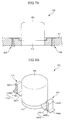
- FIG. 1 is a perspective view of an exemplary embodiment of a light emitting diode according to the present invention
- FIG. 2 is a cross-sectional view of the light emitting diode of FIG. 1 according to the present invention
- FIG. 3 is a perspective view of an exemplary embodiment of a printed circuit board on which a light emitting diode according to the present invention is mounted;
- FIG. 4A is a perspective view of an upper surface of the printed circuit board shown in FIG. 3 ;
- FIG. 4B is a perspective view of a lower surface of the printed circuit board shown in FIG. 3 ;
- FIG. 5A is a perspective view of an exemplary embodiment of the light emitting diode and the printed circuit board of FIGS. 1-4 before the light emitting diode and the printed circuit board are united with each other;
- FIG. 5B is a perspective view of an exemplary embodiment of the light emitting diode and the printed circuit board of FIGS. 1-4 after the light emitting diode and the printed circuit board are united with each other;
- FIG. 5C is a cross-sectional view of FIG. 5B ;
- FIG. 6A is a perspective view of another exemplary embodiment of a light emitting diode according to the present invention.
- FIG. 6B is a cross-sectional view of the light emitting diode shown in FIG. 6A and a printed circuit board that are united with each other;
- FIG. 7A is a perspective view of another exemplary embodiment of a light emitting diode according to the present invention.
- FIG. 7B is a cross-sectional view of the light emitting diode shown in FIG. 7A and a printed circuit board that are united with each other;
- FIG. 8A is a perspective view of another exemplary embodiment of a light emitting diode according to the present invention.
- FIG. 8B is a cross-sectional view of the light emitting diode shown in FIG. 8A and a printed circuit board that are united with each other;
- FIG. 9A is a perspective view of another exemplary embodiment of a light emitting diode according to the present invention.
- FIG. 9B is a cross-sectional view of the light emitting diode shown in FIG. 9A and a printed circuit board that are united with each other;
- FIG. 10 is an exploded perspective view of an exemplary embodiment of a liquid crystal display that includes a light source unit according to the present invention.
- first, second, third, etc. may be used herein to describe various elements, components, regions, layers and/or sections, these elements, components, regions, layers and/or sections should not be limited by these terms. These terms are only used to distinguish one element, component, region, layer or section from another region, layer or section. Thus, a first element, component, region, layer or section discussed below could be termed a second element, component, region, layer or section without departing from the teachings of the present invention.
- spatially relative terms such as “below”, “lower”, “above”, “upper” and the like, may be used herein for ease of description to describe the relationship of one element or feature to another element(s) or feature(s) as illustrated in the figures. It will be understood that the spatially relative terms are intended to encompass different orientations of the device in use or operation, in addition to the orientation depicted in the figures. For example, if the device in the figures is turned over, elements described as “below” or “lower” relative to other elements or features would then be oriented “above” relative to the other elements or features. Thus, the exemplary term “below” can encompass both an orientation of above and below. The device may be otherwise oriented (rotated 90 degrees or at other orientations) and the spatially relative descriptors used herein interpreted accordingly.
- Embodiments of the invention are described herein with reference to cross-section illustrations that are schematic illustrations of idealized embodiments (and intermediate structures) of the invention. As such, variations from the shapes of the illustrations as a result, for example, of manufacturing techniques and/or tolerances, are to be expected. Thus, embodiments of the invention should not be construed as limited to the particular shapes of regions illustrated herein but are to include deviations in shapes that result, for example, from manufacturing.
- an implanted region illustrated as a rectangle will, typically, have rounded or curved features and/or a gradient of implant concentration at its edges rather than a binary change from implanted to non-implanted region.
- a buried region formed by implantation may result in some implantation in the region between the buried region and the surface through which the implantation takes place.
- the regions illustrated in the figures are schematic in nature and their shapes are not intended to illustrate the actual shape of a region of a device and are not intended to limit the scope of the invention.
- FIG. 1 is a perspective view of an exemplary embodiment a light emitting diode according to the present invention
- FIG. 2 is a cross-sectional view of the light emitting diode of FIG. 1 according to the present invention.
- a light emitting diode 410 includes a substrate 411 , a light emitting chip 412 , wires 413 , a molding part 414 , a first lead terminal 415 , and a second lead terminal 416 .
- the light emitting chip 412 is mounted on the substrate 411 .
- the light emitting chip 412 is a semiconductor P-N junction diode.
- P- and N-type semiconductors are joined to each other and a voltage is then applied to the semiconductors, holes of the P-type semiconductor move toward the N-type semiconductor and gather at a central portion.
- electrons of the N-type semiconductor move toward the P-type semiconductor and gather at the central portion that has the lowest energy at a conduction band.
- the electrons naturally fall into holes of a valence band.
- the electrons emit energy corresponding to the difference in height between the conduction band and valence band, that is, an energy gap in the form of light.
- various types of light emitting chips may be used other than the above-mentioned light emitting chip 412 .
- the light emitting chip 412 can emit light having various wavelengths.
- the content of indium (In) used as the material of an active layer in a, for example, nitride-based light emitting diode may be adjusted, light emitting diodes for emitting light having different wavelengths may be combined with each other, or light emitting chips for emitting light having a predetermined wavelength band and phosphors are combined with each other.
- the first lead terminal 415 and the second lead terminal 416 are provided on the substrate 411 , and the wires 413 connect the light emitting chip 412 to the first lead terminal 415 and the second lead terminal 416 , respectively.
- the power is supplied to P and N electrode (not shown) of the light emitting chip 412 through the wires 413 .
- the light emitting chip 412 emits light having a predetermined wavelength.
- a molding part 414 which seals or encloses the light emitting chip 412 and the wires 413 , is formed on the substrate 411 .
- the molding part 414 may be formed in various shapes, such as, in the shape of an optical lens and in the shape of a plate. As illustrated in FIGS. 1 and 2 , the molding part 414 is formed in a substantially cylindrical.
- the molding part 414 may be made of a transparent resin, such as, liquid epoxy resin, silicon resin, or the like. Phosphors (not shown), which absorb light emitted from the light emitting chip 412 and convert the wavelength of the light into various wavelengths, may be mixed in the molding part 414 .
- the first lead terminal 415 includes a first base part 415 a and a first fitting part that protrudes from the first base part 415 a .
- the first fitting part includes a first protruding portion 415 b that protrudes from the first base part 415 a toward an upper side, e.g., toward and in a similar direction as the molding part 414 , and a first head portion 415 c formed at the end of the first protruding portion 415 b.
- the first protruding portion 415 b is inserted into a fitting hole of a printed circuit board to be described below, and the first head portion 415 c passes through the fitting hole and fits the first lead terminal 415 to the printed circuit board.
- the first head portion 415 c has a shape in which a width is gradually decreased from one end toward the other end (e.g., in a vertical direction), and is formed symmetrically about a central axis, such as, in the shape of an arrow-head.
- the first protruding portion 415 b includes a first body 415 b 1 , and a second body 415 b 2 spaced apart from the first body 415 b 1 (e.g., in a horizontal direction).
- a first end of the first body 415 b 1 is connected to a first end of the first head portion 415 c
- a first end of the second body 415 b 2 is connected to a second end of the first head portion 415 c .
- first base part 415 a extends from a second end of the first body 415 b 1 in a first direction, e.g., in a direction toward the light emitting chip 412 . Furthermore, a remaining portion of the first base part 415 a extends from a second end of the second body 415 b 2 in a second direction that is opposite to the first direction.
- the first lead terminal 415 may be formed of a single conductive plate so that the first base part 415 a , the first protruding portion 415 b , and the first head portion 415 c are continuously connected to each other, e.g., integrally formed.
- the second lead terminal 416 is symmetric with the first lead terminal 415 .
- the second lead terminal 416 includes a second base part 416 a and a second fitting part that protrudes from the second base part 416 a .
- the second fitting part includes a second protruding portion 416 b that protrudes from the second base part 416 a toward the upper side, e.g., toward the molding part 414 , and a second head portion 416 c formed at the end of the second protruding portion 416 b.
- the second protruding portion 416 b is inserted into a fitting hole of a printed circuit board to be described below, and the second head portion 416 c passes through the fitting hole and fits the second lead terminal 416 to the printed circuit board.
- the second head portion 416 c has a shape in which a width is gradually decreased from one end toward the other end, e.g., in a direction away from the distal end of the fitting part.
- the second protruding portion 416 b includes a third body 416 b 3 , and a fourth body 416 b 4 spaced apart from the third body 416 b 3 .
- a first end of the third body 416 b 3 is connected to a first end of the second head portion 416 c
- a first end of the fourth body 416 b 4 is connected to a second end of the first head portion 416 c .
- a portion of the second base part 416 a extends from a second end of the third body 416 b 3 in a first direction, e.g., in a direction toward the light emitting chip 412 .
- a remaining portion of the second base part 416 a extends from a second end of the fourth body 416 b 4 in a second direction that is opposite to the first direction.
- each of the first lead terminal 415 and the second lead terminal 416 includes a fitting part.
- each of the lead terminals may include a plurality of fitting parts.
- the number of fitting holes into which the fitting parts are fitted corresponds to that of the fitting parts, and the shape of each fitting hole corresponds to that of each fitting part.
- “corresponds” is used to indicate corresponding substantially in shape, dimension and/or positional placement.
- FIG. 3 is a perspective view of an exemplary embodiment of a printed circuit board on which a light emitting diode according to the present invention is mounted
- FIG. 4A is a perspective view of an upper surface of the printed circuit board shown in FIG. 3
- FIG. 4B is a perspective view of a lower surface of the printed circuit board shown in FIG. 3 .
- a printed circuit board 470 includes a base plate 471 , such as made of an insulating material, circuit patterns 472 formed on the base plate 471 , and a fitting hole formed in the base plate 471 .
- the fitting hole includes first and second fitting holes 475 and 476 and a third fitting hole 477 .
- the lead terminals of the light emitting diode 410 shown in FIGS. 1 and 2 are fitted into the first and second fitting holes 475 and 476 , respectively.
- the body of the light emitting diode, e.g., the molding part 414 and/or substrate 411 passes through the third fitting hole 477 of the printed circuit board 470 .
- the first fitting hole 475 and the second fitting hole 476 are formed in the base plate 471 on a region of the base plate 471 where the circuit patterns 472 are formed, and the third fitting hole 477 is formed between the first fitting hole 475 and the second fitting hole 476 .
- the circuit patterns 472 may extend into the first fitting hole 475 and the second fitting hole 476 .
- Sizes and shapes of the first and second fitting holes 475 and 476 correspond to sizes and shapes of the first fitting part of the first lead terminal 415 and the second fitting part of the second lead terminal 416 , respectively.
- a size and shape of the third fitting hole 477 corresponds to a size and shape of the molding part 414 and/or substrate 411 of the LED 410 .
- Various types of printed circuit boards may be used as the printed circuit board on which the light emitting diode according to the present invention is mounted.
- a rigid printed circuit board, a metal core printed circuit board, an FR4 printed circuit board (Flame Retardant Type 4 substrate, such as, a fire retardant substrate made of glass fiber and epoxy resin), or the like may be used as the printed circuit board according to the present invention.
- FIG. 5A is a perspective view of an exemplary embodiment of the light emitting diode and the printed circuit board of FIGS. 1-4 before the light emitting diode and the printed circuit board are united with each other
- FIG. 5B is a perspective view of an exemplary embodiment of the light emitting diode and the printed circuit board of FIGS. 1-4 after the light emitting diode and the printed circuit board are united with each other
- FIG. 5C is a cross-sectional view of FIG. 5B .
- a light source unit includes the light emitting diode 410 and the printed circuit board 470 on which the light emitting diode 410 is mounted.
- the light emitting diode 410 includes the substrate 411 , the light emitting chip 412 , the wires 413 , the molding part 414 , the first lead terminal 415 that includes of the first base part 415 a and the first fitting part, and the second lead terminal 416 that includes the second base part 416 a and the second fitting part.
- the printed circuit board 470 includes the base plate 471 , the circuit patterns 472 formed on a surface of the base plate 471 (e.g., such as the single upper surface), and the first to third fitting holes 475 , 476 , and 477 that are formed in the base plate 471 .
- the light emitting diode 410 is combined with the printed circuit board 470 from the rear side of the printed circuit board 470 .
- the light emitting diode 410 is aligned with the printed circuit board 470 so as to be combined with the printed circuit board 470 from one surface of the printed circuit board 470 , e.g., the surface of the printed circuit board opposite to the surface thereof on which the circuit patterns 472 are formed, toward an opposing surface of the printed circuit board, e.g., where the circuit patterns are formed 472 .
- the first fitting part of the first lead terminal 415 of the light emitting diode 410 is fitted into the first fitting hole 475 of the printed circuit board 470
- the second fitting part of the second lead terminal 416 is fitted into the second fitting hole 476 of the printed circuit board 470 .
- the molding part 414 passes through the third fitting hole 477 , and is disposed on one surface of the printed circuit board, e.g., a front surface such as where the circuit patterns 472 are formed.
- first and second lead terminals 415 and 416 of the light emitting diode 410 are combined with the printed circuit board 470 .
- the lead terminals are symmetrical with each other. Accordingly, the only first lead terminal 415 will be described below.
- the first protruding portion 415 b of the LED 410 is disposed in the first fitting hole 475 .
- the first head portion 415 c is disposed on a surface of the printed circuit board 470 , such as, on the surface thereof on which the circuit patterns 472 are formed.
- the first base part 415 a of the LED 410 is disposed on an opposing surface of the printed circuit board 470 , such as, on the surface thereof opposite to the surface on which the circuit patterns 472 are formed (e.g., a rear side).
- the first lead terminal 415 is fitted into the first fitting hole 475 .
- the first head portion 415 c comes in contact with the circuit patterns 472 formed on the printed circuit board 470 .
- a lower surface of the first head portion 415 c contacts an upper surface of the printed circuit board 470 as a portion where the circuit patterns 472 are formed, as illustrated in FIG. 5C .
- the first lead terminal 415 of the LED 410 is electrically connected to the circuit patterns 472 of the printed circuit board 470 without having to perform an additional assembly step and without requiring additional parts, such as solder.
- the circuit patterns 472 When the circuit patterns 472 extend into the first fitting hole 475 , since the first protruding portion 415 b of the first lead terminal 415 of the LED 410 comes in contact with the circuit patterns 472 in the first fitting hole 475 of the printed circuit board 470 , the first lead terminal 415 is electrically connected to the circuit patterns 472 .
- the circuit patterns 472 are formed in the first fitting hole 475 as described above, a contact area between the first lead terminal 415 of the LED 410 and the circuit patterns 472 of the printed circuit board 470 is increased.
- the first head portion 415 c has a shape in which a width is gradually decreased from one end toward the other end, e.g., in a direction away from the distal end of the fitting part.
- the first head portion 415 c is considered to have a tapered shape.
- the first head portion 415 c has predetermined elasticity.
- a width of the first head portion 415 c inserted into the first fitting hole 475 is decreased or deformed.
- the width decreasing is a result of the first body 415 b 1 and the second body 415 b 2 being moved toward each other as wider portions of the tapered first head portion 415 c successively pass through the first fitting hole 475 in a direction from the rear side to the front side of the printed circuit board 470 . As a result, it is possible to relatively easily insert the first head portion 415 c into the first fitting hole 475 .
- the first head portion 415 c After the first head portion 415 c completely passes through the first fitting hole 475 , the first head portion 415 c is restored to the original shape, e.g., the first body 415 b 1 and the second body 415 b 2 are moved away from each other by a restoring force of the elasticity. Since the first head portion 415 c is secured in the first fitting hole 475 of the printed circuit board 470 , the first lead terminal 415 can be securely combined with the printed circuit board 470 .
- FIG. 6A is a perspective view of another exemplary embodiment of a light emitting diode according to the present invention
- FIG. 6B is a cross-sectional view of the light emitting diode shown in FIG. 6A and a printed circuit board that are united with each other.
- a light emitting diode of FIG. 6A and has substantially the same structure as the light emitting diode of FIG. 1 -, except for the position of a fitting part and a direction in which a light emitting diode is combined with a printed circuit board. Accordingly, only the differences between the first and second embodiments will be described below.
- a light emitting diode 420 includes a substrate 421 , a light emitting chip, wires, a molding part 424 , a first lead terminal 425 , and a second lead terminal 426 .
- the first lead terminal 425 includes a first base part 425 a and a first fitting part that protrudes from the first base part 425 a .
- the first fitting part includes a first protruding portion 425 b that protrudes from the first base part 425 a toward a lower side, e.g., toward a side of the LED 420 opposite to the molding part 424 , and a first head portion 425 c formed at the end of the first protruding portion 425 b.
- the first protruding portion 425 b is inserted into a fitting hole of a printed circuit board to be described below, and the first head portion 425 c passes through the fitting hole and fits the first lead terminal 425 to the printed circuit board.
- the first head portion 425 c has a shape in which a width is gradually decreased from one end toward the other end, e.g., in a direction of the first fitting part toward the distal end.
- the first protruding portion 425 b includes a first body 425 b 1 , and a second body 425 b 2 spaced apart from the first body 425 b 1 .
- a first end of the first body 425 b 1 is connected to a first end of the first head portion 425 c
- a first end of the second body 425 b 2 is connected to a second end of the first head portion 425 c
- a portion of the first base part 425 a extends from a second end of the first body 425 b 1 in a first direction, e.g., in a direction toward the molding part 424 .
- a remaining portion of the first base part 425 a extends from a second end of the second body 425 b 2 in a second direction that is opposite to the first direction, e.g., away from the molding part 424 of the LED 420 .
- the second lead terminal 426 is symmetrical with the first lead terminal 425 .
- the second lead terminal 426 includes a second base part 426 a and a second fitting part that protrudes from the second base part 426 a .
- the second fitting part includes a second protruding portion 426 b that protrudes from the second base part 426 a toward a lower side of the LED 420 , e.g., toward a side opposite to the molding part 424 , and a second head portion 426 c formed at the end of the second protruding portion 426 b .
- the second protruding portion 426 b includes a third body 426 b 3 , and a fourth body 426 b 4 spaced apart from the third body 426 b 3 .
- the light emitting diode 420 is combined with the printed circuit board 470 from a front side (e.g., upper side) of the printed circuit board.
- the light emitting diode 420 is aligned with the printed circuit board so as to be combined with the printed circuit board when the LED 420 is inserted from a single surface of the printed circuit board, such as, the surface of the printed circuit board on which the circuit patterns 472 are formed, toward the other surface of the printed circuit board, e.g., where the circuit patterns are not formed.
- the first fitting part of the first lead terminal 425 of the light emitting diode 420 is fitted into the first fitting hole 475 of the printed circuit board, and the second fitting part of the second lead terminal 426 is fitted into the second fitting hole 476 .
- the substrate 421 of the LED 420 passes through the third fitting hole 477 , and is disposed on a surface of the printed circuit board, such as where the circuit patterns are not formed.
- first and second lead terminals 425 and 426 of the light emitting diode 420 are combined with the printed circuit board 470 .
- the lead terminals are symmetrical with each other. Accordingly, only the first lead terminal 425 will be described below.
- the first protruding portion 425 b is disposed in the first fitting hole 475 .
- the first base part 425 a is disposed on one surface of the printed circuit board 470 , e.g., on an upper surface thereof on which the circuit patterns 472 are formed.
- the first head portion 425 c of the LED 420 is disposed on another surface of the printed circuit board 470 , e.g., on an opposing surface to the surface on which the circuit patterns 472 are formed.
- the first lead terminal 425 of the LED 420 is fitted into the first fitting hole 475 of the printed circuit board 470 .
- the first base part 425 a comes in contact with the circuit patterns 472 formed the upper surface on the printed circuit board 470 .
- the first lead terminal 425 is electrically connected to the circuit patterns 472 without having to additionally solder the LED 420 to the printed circuit board 470 .
- the circuit patterns 472 are formed on one surface, e.g., the upper surface of the printed circuit board 470 .
- the invention is not limited thereto, and the circuit patterns 472 may be formed on another surface, e.g., a lower surface of the printed circuit board.
- the LED 420 can be electrically connected to the printed circuit board 470 regardless if the circuit patterns are formed on the upper surface or the lower surface of the printed circuit board 470 .
- FIG. 7A is a perspective view of another exemplary embodiment of a light emitting diode according to the present invention
- FIG. 7B is a cross-sectional view of the light emitting diode shown in FIG. 7A and a printed circuit board that are united with each other.
- a light emitting diode of FIG. 7A and has substantially the same structure as the light emitting diode of FIG. 6A and, except for the shape of a fitting part. Accordingly, only differences between the LED's of FIGS. 6 A/ 6 B and 7 A/will be described below.
- a light emitting diode 430 includes a substrate 431 , a light emitting chip, wires, a molding part 434 , a first lead terminal 435 , and a second lead terminal 436 .
- the first lead terminal 435 includes a first base part 435 a and a first fitting part that protrudes from the first base part 435 a .
- the first fitting part includes a first protruding portion 435 b that protrudes from the first base part 435 a toward the lower side, e.g., toward the side opposite to the molding part 434 , and a first head portion 435 c formed at the end of the first protruding portion 435 b.
- the first protruding portion 435 b includes a first body 435 b 1 and a second body 435 b 2 .
- the first body 435 b is formed on one surface, e.g., the lower surface of the first base part 435 a .
- the second body 435 b 2 is formed on the lower surface of the first base part 435 a and spaced apart from the first body 435 b 1 .
- the first head portion 435 c includes a first head 435 c 1 and a second head 435 c 2 .
- the first head 435 c 1 protrudes from the end of the first body 435 b 1 in a lateral direction, e.g., substantially perpendicular to the first body 435 b 1 .
- the second head 435 c 2 protrudes from the end of the second body 435 b 2 in a lateral direction, e.g., substantially perpendicular to the second body 435 b 2 .
- the second protruding portion 436 b includes a third body 436 b 3 , and a fourth body 436 b 4 spaced apart from the third body 436 b 3 .
- the first head portion 435 c is formed at the ends of the first and second bodies 435 b 1 and 435 b 2 , respectively.
- the present invention is not limited thereto.
- the first head portion 435 c may connect the distal end of the first body 435 b 1 to the end of the second body 435 b 2 , e.g., forming the first head portion 435 c as described in FIGS. 1-6 .
- the second head portion 436 c includes a third head 436 c 3 and a fourth head 435 c 4 .
- the third head 435 c 3 protrudes from the end of the third body 436 b 3 in a lateral direction, e.g., substantially perpendicular to the third body 435 b 3 .
- the fourth head 435 c 4 protrudes from the end of the fourth body 435 b 4 in a lateral direction, e.g., substantially perpendicular to the fourth body 435 b 4 .
- the first protruding portion 435 b includes two bodies.
- the present invention is not limited thereto, and the first and/or protruding portion 435 b and 436 b may include three or more bodies that are spaced apart from each other.
- the first and/or second head portion 435 c and 436 c may include three or more heads that are formed at the ends of the bodies, respectively.
- the head portions may extend in same or different lateral directions from the bodies, so long as the head portions are configured to connect the light emitting diode to the printed circuit board.
- a body portion of the three or more bodies may not have a head portion disposed at a distal end thereof.
- the light emitting diode 430 is combined with the printed circuit board 470 from the front side of the printed circuit board 470 .
- the first head portion 435 c of the first lead terminal 435 of the light emitting diode 430 is inserted through the first fitting hole 475 of the printed circuit board 470
- the first protruding portion 435 b is disposed in the first fitting hole 475 .
- the first base part 435 a is disposed on the upper surface of the printed circuit board 470 , e.g., on the surface thereof on which the circuit patterns 472 are formed.
- the first head portion 435 c is disposed on the lower surface of the printed circuit board 470 , e.g., on the surface thereof opposite to the surface on which the circuit patterns 472 are formed.
- the first lead terminal 435 is fitted into the first fitting hole 475 of the printed circuit board 470 .
- the first base part 435 a comes in contact with the circuit patterns 472 formed on the printed circuit board 470 .
- the first lead terminal 435 of the LED 430 is electrically connected to the circuit patterns 472 of the circuit board 470 without having to additionally solder the components together.
- FIG. 8A is a perspective view of another exemplary embodiment of a light emitting diode according to the present invention
- FIG. 8B is a cross-sectional view of the light emitting diode shown in FIG. 8A and a printed circuit board that are united with each other.
- a light emitting diode of FIGS. 8A and 8B has substantially the same structure as the light emitting diode of FIG. 1 -, except for the shape of a head portion. Accordingly, only the differences between the light emitting will be described below.
- a light emitting diode 440 includes a substrate 441 , a light emitting chip, wires, a molding part 444 , a first lead terminal 445 , and a second lead terminal 446 .
- the first lead terminal 445 includes a first base part 445 a and a first fitting part that protrudes from the first base part 445 a .
- the first fitting part includes a first protruding portion 445 b and a first head portion 445 c .
- the first protruding portion 445 b protrudes from the first base part 445 a toward the upper side, e.g., toward the molding part 444 .
- the first head portion 445 c is formed at the distal end of the first protruding portion 445 b .
- the first protruding portion 445 b includes a first body 445 b 1 , and a second body 445 b 2 spaced apart from the first body 445 b 1 (e.g., in a horizontal direction).
- the second lead terminal 446 is symmetric with the first lead terminal 445 .
- the second lead terminal 446 includes a second base part 446 a and a second fitting part that protrudes from the second base part 446 a .
- the second fitting part includes a second protruding portion 446 b that protrudes from the second base part 446 a toward the upper side, e.g., toward the molding part 444 , and a second head portion 446 c formed at the end of the second protruding portion 446 b .
- the second protruding portion 446 b includes a third body 446 b 3 , and a fourth body 446 b 4 spaced apart from the third body 446 b 3 .
- the first head portion 445 c has a shape in which a width is gradually decreased from one end toward the other end, e.g. in a direction from the first base part 445 a to the distal end of the first protruding portion 445 b .
- the first head portion 445 c of FIGS. 8A and 8B is formed unsymmetrically with respect to a central (vertical) axis.
- the first head portion 445 c is considered to have a profile in the shape of a hook, whereby one side is substantially flat or vertical and an opposing side of the first head portion 445 c is tapered.
- FIG. 9A is a perspective view of another exemplary embodiment of a light emitting diode according to the present invention
- FIG. 9B is a cross-sectional view of the light emitting diode shown in FIG. 9A and a printed circuit board that are united with each other.
- a light emitting diode 450 includes a substrate 451 , a light emitting chip, wires, a molding part 454 , a first lead terminal 455 , and a second lead terminal 456 .
- the first lead terminal 455 includes a first base part 455 a and a first fitting part that protrudes from the first base part 455 a .
- the first fitting part includes a first protruding portion 455 b and a first head portion 455 c .
- the first protruding portion 455 b extends from the end of the first base part 455 a and is bent toward the upper side of the LED 450 from the first base part 455 a and toward the molding part 454 .
- the first head portion 455 c is formed at the end of the first protruding portion 455 b.
- the first head portion 455 c has a shape in which a width is gradually decreased from one end toward the other end, e.g., in a direction from the first base part 455 a toward the distal end of the first protruding portion 455 b .
- One surface of the head portion 455 c is flat and the other surface thereof is inclined. The flat surface is on an inner aide of the first head portion 455 c , but the invention is not limited thereto.
- the flat side of the first head portion 455 c may be out the outermost side of the first head portion 455 c relative to the LED 459 .
- the first head portion 455 c passes through the first fitting hole 475 of the printed circuit board 470 , and fits the first lead terminal 455 to the printed circuit board.
- the second lead terminal 456 includes a first base part 456 a and a first fitting part that protrudes from the first base part 456 a .
- the first fitting part includes a first protruding portion 456 b and a first head portion 456 c .
- the first protruding portion 456 b extends from the end of the first base part 456 a and is bent toward the upper side of the LED 450 from the first base part 456 and toward the molding part 454 .
- the first head portion 456 c is formed at the end of the first protruding portion 456 b.
- FIG. 10 is an exploded perspective view of an exemplary embodiment of a liquid crystal display that includes a light source unit according to the present invention.
- a liquid crystal display includes an upper sash 300 , a liquid crystal panel 100 , driving circuit units 220 and 240 , a diffusion plate 600 , a plurality of optical sheets 700 , a light source unit 400 , a mold frame 800 , and a lower sash 900 .
- a predetermined receiving space is formed in the mold frame 800 .
- a backlight unit which includes the diffusion plate 600 , the plurality of optical sheets 700 , and the light source unit 400 , is disposed in the receiving space of the mold frame 800 .
- the liquid crystal panel 100 displaying images is disposed above the backlight unit.
- the driving circuit unit 220 includes a gate printed circuit board 224 and a flexible gate printed circuit board 222 .
- the driving circuit unit 240 includes a flexible data printed circuit board 242 and a data printed circuit board 244 .
- the gate printed circuit board 224 is connected to the liquid crystal panel 100 , includes control ICs (integrated circuits) mounted thereon, and supplies predetermined gate signals to gate lines of a TFT substrate 120 .
- the data printed circuit board 244 includes control ICs mounted thereon, and supplies predetermined data signals to data lines of the TFT substrate 120 .
- the flexible gate printed circuit board 222 connects the TFT substrate 120 with the gate printed circuit board 224
- the flexible data printed circuit board 242 connects the TFT substrate 120 with the data printed circuit board 244 .
- the gate and data printed circuit boards 224 and 244 are connected to the flexible gate printed circuit board 222 and the data printed circuit board 242 , respectively, to supply gate driving signals and external image signals.
- the gate and data printed circuit boards 224 and 244 may be integrated as one printed circuit board. As used herein, “integrated” is used to mean that the gate and data printed circuit boards are a single unit.
- Each of the flexible printed circuit boards 222 and 242 includes a driving IC mounted thereon to transmit RGB (Red, Green, and Blue) signals and electrical power, which are generated from the printed circuit boards 224 and 244 , to the liquid crystal panel 100 .
- the light source unit 400 includes light emitting diodes, such as light emitting diodes 410 , 420 , 430 , 440 and/or 450 of the illustrated embodiments in FIGS. 1-9 , and a printed circuit board 470 .
- Each of the light emitting diodes 410 to 450 includes the above-mentioned fitting parts, and is fitted to the printed circuit board 470 so as to be mounted on the printed circuit board 470 .
- the diffusion plate 600 and the plurality of optical sheets 700 are disposed above the light source unit 400 to create a uniform brightness distribution of light emitted from the light source unit 400 .
- the optical sheets 700 may include, but are not limited to, a prism sheet and a diffusion sheet.
- the upper sash 300 is united with the mold frame 800 so as to cover edge portions (e.g., non-display regions) of the liquid crystal panel 100 and side and lower surfaces of the mold frame 800 .
- the lower sash 900 is provided below the mold frame 800 and closes the receiving space of the mold frame 800 .
- the light emitting diode when a light emitting diode is mounted on a printed circuit board, the light emitting diode is fitted to the printed circuit board so as to be mounted on the printed circuit board without having to solder as described above. Accordingly, if defects occur in the light emitting diode mounted on the printed circuit board, it is possible to separate the defective light emitting diode from the printed circuit board and to replace the defective light emitting diode with another light emitting diode. Therefore, it is possible to perform rework.
- it is possible to reduce cost of materials and to reduce the manufacturing cost of the light source unit.
Abstract
Description
Claims (18)
Applications Claiming Priority (2)
| Application Number | Priority Date | Filing Date | Title |
|---|---|---|---|
| KR10-2006-0109639 | 2006-11-07 | ||
| KR1020060109639A KR101249989B1 (en) | 2006-11-07 | 2006-11-07 | Light source unit, backlight unit and liquid crystal display having the same |
Publications (2)
| Publication Number | Publication Date |
|---|---|
| US20080106898A1 US20080106898A1 (en) | 2008-05-08 |
| US7766499B2 true US7766499B2 (en) | 2010-08-03 |
Family
ID=39359552
Family Applications (1)
| Application Number | Title | Priority Date | Filing Date |
|---|---|---|---|
| US11/936,501 Active 2028-06-12 US7766499B2 (en) | 2006-11-07 | 2007-11-07 | Light source unit, backlight unit and liquid crystal display including the same, and method thereof |
Country Status (2)
| Country | Link |
|---|---|
| US (1) | US7766499B2 (en) |
| KR (1) | KR101249989B1 (en) |
Cited By (4)
| Publication number | Priority date | Publication date | Assignee | Title |
|---|---|---|---|---|
| US20110149569A1 (en) * | 2009-12-23 | 2011-06-23 | Au Optronics Corporation | Light-emitting diode module |
| US20130146347A1 (en) * | 2011-12-13 | 2013-06-13 | Kemet Electronics Corporation | High aspect ratio stacked mlcc design |
| US20170257943A1 (en) * | 2014-09-12 | 2017-09-07 | Ledil Oy | A circuit board system |
| US20180247768A1 (en) * | 2015-02-27 | 2018-08-30 | Epcos Ag | Electrical component and a method for producing an electrical component |
Families Citing this family (10)
| Publication number | Priority date | Publication date | Assignee | Title |
|---|---|---|---|---|
| WO2010070955A1 (en) * | 2008-12-18 | 2010-06-24 | シャープ株式会社 | Lighting device, display device, and television receiving device |
| KR101020992B1 (en) * | 2009-03-02 | 2011-03-09 | 엘지이노텍 주식회사 | Light emitting module and light unit having the same |
| US20110090259A1 (en) * | 2009-10-16 | 2011-04-21 | Samsung Electronics Co., Ltd. | Light emitting module, backlight unit and display apparatus |
| KR101719693B1 (en) | 2010-05-11 | 2017-03-27 | 삼성디스플레이 주식회사 | Light emitting diode package and display apparatus having the same |
| TWM404393U (en) * | 2010-11-10 | 2011-05-21 | Chunghwa Picture Tubes Ltd | Light bar structure and display device |
| KR102078645B1 (en) | 2013-06-03 | 2020-02-19 | 삼성전자 주식회사 | Inductor and display apparatus including the same |
| CN204084030U (en) * | 2014-09-11 | 2015-01-07 | 深圳Tcl新技术有限公司 | Led module and display |
| DE102014224033A1 (en) * | 2014-11-25 | 2016-05-25 | Robert Bosch Gmbh | Electronic module, in particular for vehicle transmission control unit, with press-contact sandwich module technology |
| WO2018074693A1 (en) * | 2016-10-21 | 2018-04-26 | 엘지전자 주식회사 | Display device |
| CN108679573A (en) * | 2018-05-31 | 2018-10-19 | 华域视觉科技(上海)有限公司 | LED light source face illuminating module and apply its car light |
Citations (27)
| Publication number | Priority date | Publication date | Assignee | Title |
|---|---|---|---|---|
| US5068771A (en) * | 1991-04-29 | 1991-11-26 | Savage John Jun | Reflector lens cap and/or clip for LED |
| JPH0548150A (en) | 1991-08-07 | 1993-02-26 | Seiko Epson Corp | Position control elimination preventive light emitting diode |
| JPH067184A (en) | 1992-06-26 | 1994-01-18 | Nippon Shinyaku Co Ltd | Production of maltobionic acid |
| JPH07297452A (en) | 1994-04-27 | 1995-11-10 | Rohm Co Ltd | Structure and method for temporarily fixing parts mounted on substrate to substrate |
| JPH08221008A (en) | 1995-02-20 | 1996-08-30 | Sanyo Electric Co Ltd | Display device |
| US5726862A (en) * | 1996-02-02 | 1998-03-10 | Motorola, Inc. | Electrical component having formed leads |
| JPH10289971A (en) | 1997-04-16 | 1998-10-27 | Matsushita Electric Ind Co Ltd | Led fixing device |
| KR19990001425U (en) | 1997-06-19 | 1999-01-15 | 배순훈 | Diode flow prevention structure of electronic product |
| KR19990023242U (en) | 1997-12-04 | 1999-07-05 | 전주범 | Diode holder |
| KR20000005595U (en) | 1998-08-31 | 2000-03-25 | 전주범 | Light Emitting Diode Holder for Electronics |
| US6152568A (en) | 1998-02-05 | 2000-11-28 | Toshiba Lighting & Technology Corporation | Lighting apparatus and display apparatus having the same |
| JP2001044507A (en) | 1999-07-26 | 2001-02-16 | Ichikoh Ind Ltd | Fixation structure for light emitting diode |
| US6252350B1 (en) | 1998-07-31 | 2001-06-26 | Andres Alvarez | Surface mounted LED lamp |
| US20020036464A1 (en) | 2000-09-26 | 2002-03-28 | Kabushiki Kaisha Toshiba | Led lamp, led lamp assembly and fixing method of an led lamp |
| US6386733B1 (en) * | 1998-11-17 | 2002-05-14 | Ichikoh Industries, Ltd. | Light emitting diode mounting structure |
| KR20020052785A (en) | 2000-12-26 | 2002-07-04 | 박종섭 | device for fixed LED of electron machinery and tools |
| US20020117954A1 (en) | 2001-02-28 | 2002-08-29 | Harison Toshiba Lighting Corporation | Device for mounting a light source |
| US20040004227A1 (en) | 2002-07-04 | 2004-01-08 | Kiyoshi Tateishi | Unit for driving light-emitting device |
| KR200359158Y1 (en) | 2004-05-04 | 2004-08-21 | 김진우 | Light effusing structure where light emitting diodes are replaceable |
| KR20040080626A (en) | 2003-03-12 | 2004-09-20 | 강석구 | A signboard using LED |
| US6923548B2 (en) * | 2000-12-13 | 2005-08-02 | Lg.Philips Lcd Co., Ltd. | Backlight unit in liquid crystal display |
| JP2005311102A (en) | 2004-04-22 | 2005-11-04 | Matsushita Electric Ind Co Ltd | Led holder |
| KR20060002326A (en) | 2004-07-01 | 2006-01-09 | 서울반도체 주식회사 | Monochromatic light emitting diode package with improved heat protection rate |
| US20060076570A1 (en) | 2004-10-08 | 2006-04-13 | Chen Yen C | SMD(surface mount device)-type light emitting diode with high heat dissipation efficiency and high power |
| KR20060053468A (en) | 2004-11-16 | 2006-05-22 | 엘지이노텍 주식회사 | Led package having multitude led |
| KR20060083676A (en) | 2005-01-18 | 2006-07-21 | 주식회사 현대오토넷 | Light emitting diode assembly |
| US7341371B2 (en) * | 2005-10-21 | 2008-03-11 | Tyc Brother Industrial Co., Ltd. | LED light assembly with LED connecting device |
Family Cites Families (4)
| Publication number | Priority date | Publication date | Assignee | Title |
|---|---|---|---|---|
| US6517218B2 (en) * | 2000-03-31 | 2003-02-11 | Relume Corporation | LED integrated heat sink |
| KR20060036292A (en) * | 2004-10-25 | 2006-04-28 | 삼성전자주식회사 | Display apparatus |
| TWI247439B (en) | 2004-12-17 | 2006-01-11 | Genesis Photonics Inc | Light-emitting diode device |
| KR101142519B1 (en) * | 2005-03-31 | 2012-05-08 | 서울반도체 주식회사 | Backlight panel employing white light emitting diode having red phosphor and green phosphor |
-
2006
- 2006-11-07 KR KR1020060109639A patent/KR101249989B1/en active IP Right Grant
-
2007
- 2007-11-07 US US11/936,501 patent/US7766499B2/en active Active
Patent Citations (27)
| Publication number | Priority date | Publication date | Assignee | Title |
|---|---|---|---|---|
| US5068771A (en) * | 1991-04-29 | 1991-11-26 | Savage John Jun | Reflector lens cap and/or clip for LED |
| JPH0548150A (en) | 1991-08-07 | 1993-02-26 | Seiko Epson Corp | Position control elimination preventive light emitting diode |
| JPH067184A (en) | 1992-06-26 | 1994-01-18 | Nippon Shinyaku Co Ltd | Production of maltobionic acid |
| JPH07297452A (en) | 1994-04-27 | 1995-11-10 | Rohm Co Ltd | Structure and method for temporarily fixing parts mounted on substrate to substrate |
| JPH08221008A (en) | 1995-02-20 | 1996-08-30 | Sanyo Electric Co Ltd | Display device |
| US5726862A (en) * | 1996-02-02 | 1998-03-10 | Motorola, Inc. | Electrical component having formed leads |
| JPH10289971A (en) | 1997-04-16 | 1998-10-27 | Matsushita Electric Ind Co Ltd | Led fixing device |
| KR19990001425U (en) | 1997-06-19 | 1999-01-15 | 배순훈 | Diode flow prevention structure of electronic product |
| KR19990023242U (en) | 1997-12-04 | 1999-07-05 | 전주범 | Diode holder |
| US6152568A (en) | 1998-02-05 | 2000-11-28 | Toshiba Lighting & Technology Corporation | Lighting apparatus and display apparatus having the same |
| US6252350B1 (en) | 1998-07-31 | 2001-06-26 | Andres Alvarez | Surface mounted LED lamp |
| KR20000005595U (en) | 1998-08-31 | 2000-03-25 | 전주범 | Light Emitting Diode Holder for Electronics |
| US6386733B1 (en) * | 1998-11-17 | 2002-05-14 | Ichikoh Industries, Ltd. | Light emitting diode mounting structure |
| JP2001044507A (en) | 1999-07-26 | 2001-02-16 | Ichikoh Ind Ltd | Fixation structure for light emitting diode |
| US20020036464A1 (en) | 2000-09-26 | 2002-03-28 | Kabushiki Kaisha Toshiba | Led lamp, led lamp assembly and fixing method of an led lamp |
| US6923548B2 (en) * | 2000-12-13 | 2005-08-02 | Lg.Philips Lcd Co., Ltd. | Backlight unit in liquid crystal display |
| KR20020052785A (en) | 2000-12-26 | 2002-07-04 | 박종섭 | device for fixed LED of electron machinery and tools |
| US20020117954A1 (en) | 2001-02-28 | 2002-08-29 | Harison Toshiba Lighting Corporation | Device for mounting a light source |
| US20040004227A1 (en) | 2002-07-04 | 2004-01-08 | Kiyoshi Tateishi | Unit for driving light-emitting device |
| KR20040080626A (en) | 2003-03-12 | 2004-09-20 | 강석구 | A signboard using LED |
| JP2005311102A (en) | 2004-04-22 | 2005-11-04 | Matsushita Electric Ind Co Ltd | Led holder |
| KR200359158Y1 (en) | 2004-05-04 | 2004-08-21 | 김진우 | Light effusing structure where light emitting diodes are replaceable |
| KR20060002326A (en) | 2004-07-01 | 2006-01-09 | 서울반도체 주식회사 | Monochromatic light emitting diode package with improved heat protection rate |
| US20060076570A1 (en) | 2004-10-08 | 2006-04-13 | Chen Yen C | SMD(surface mount device)-type light emitting diode with high heat dissipation efficiency and high power |
| KR20060053468A (en) | 2004-11-16 | 2006-05-22 | 엘지이노텍 주식회사 | Led package having multitude led |
| KR20060083676A (en) | 2005-01-18 | 2006-07-21 | 주식회사 현대오토넷 | Light emitting diode assembly |
| US7341371B2 (en) * | 2005-10-21 | 2008-03-11 | Tyc Brother Industrial Co., Ltd. | LED light assembly with LED connecting device |
Cited By (10)
| Publication number | Priority date | Publication date | Assignee | Title |
|---|---|---|---|---|
| US20110149569A1 (en) * | 2009-12-23 | 2011-06-23 | Au Optronics Corporation | Light-emitting diode module |
| US8052302B2 (en) * | 2009-12-23 | 2011-11-08 | Au Optronics Corporation | Light-emitting diode module |
| US20130146347A1 (en) * | 2011-12-13 | 2013-06-13 | Kemet Electronics Corporation | High aspect ratio stacked mlcc design |
| US8988857B2 (en) * | 2011-12-13 | 2015-03-24 | Kemet Electronics Corporation | High aspect ratio stacked MLCC design |
| US20170257943A1 (en) * | 2014-09-12 | 2017-09-07 | Ledil Oy | A circuit board system |
| US10165676B2 (en) * | 2014-09-12 | 2018-12-25 | Ledil Oy | Circuit board system |
| US20180247768A1 (en) * | 2015-02-27 | 2018-08-30 | Epcos Ag | Electrical component and a method for producing an electrical component |
| US10395843B2 (en) | 2015-02-27 | 2019-08-27 | Epcos Ag | Electrical connection contact for a ceramic component, a ceramic component, and a component arrangement |
| US10943740B2 (en) | 2015-02-27 | 2021-03-09 | Epcos Ag | Electrical connection contact for a ceramic component, a ceramic component, and a component arrangement |
| US11342126B2 (en) * | 2015-02-27 | 2022-05-24 | Epcos Ag | Electrical component and a method for producing an electrical component |
Also Published As
| Publication number | Publication date |
|---|---|
| US20080106898A1 (en) | 2008-05-08 |
| KR101249989B1 (en) | 2013-04-01 |
| KR20080041494A (en) | 2008-05-13 |
Similar Documents
| Publication | Publication Date | Title |
|---|---|---|
| US7766499B2 (en) | Light source unit, backlight unit and liquid crystal display including the same, and method thereof | |
| US7775681B2 (en) | Lighting device, backlight unit, and printed circuit board thereof | |
| US8439513B2 (en) | Light emitting diode module and back light assembly | |
| US8668352B2 (en) | Light emitting module | |
| US8864357B2 (en) | Light emitting device and light unit having the same | |
| US7936415B2 (en) | Light source apparatus and liquid crystal display having the same | |
| US7646450B2 (en) | Light emitting diode array, method of manufacturing the same, backlight assembly having the same, and LCD having the same | |
| CN110212072B (en) | Molded surface mount device LED display module | |
| US20080048203A1 (en) | Light Emitting Apparatus, Manufacturing Method Thereof, and Light Unit | |
| US20090146159A1 (en) | Light-emitting device, method of manufacturing the light-emitting device and liquid crystal display having the light-emitting device | |
| US20070001564A1 (en) | Light emitting diode package in backlight unit for liquid crystal display device | |
| KR101705700B1 (en) | Light Emitting Diode | |
| US7815330B2 (en) | Backlight assembly and display device having the same | |
| US20050254260A1 (en) | Light positioning device | |
| CN110865485A (en) | Illumination device and display device provided with illumination device | |
| US8052302B2 (en) | Light-emitting diode module | |
| TWI457514B (en) | Lighting device | |
| US20090065797A1 (en) | Light emitting unit and liquid crystal display device using the same | |
| US20100117102A1 (en) | Light emitting diodes and backlight unit having the same | |
| KR102327463B1 (en) | Liquid crystal display device | |
| KR101676670B1 (en) | Light Emitting Diode | |
| US20120170290A1 (en) | Light emitting diode package module and method of manufacturing the same | |
| TWI407398B (en) | Lighting device, backlight unit, and printed circuit board thereof | |
| KR101894933B1 (en) | Light Emitting Device Package |
Legal Events
| Date | Code | Title | Description |
|---|---|---|---|
| AS | Assignment |
Owner name: SAMSUNG ELECTRONICS CO., LTD., KOREA, REPUBLIC OF Free format text: ASSIGNMENT OF ASSIGNORS INTEREST;ASSIGNORS:BAE, HYUN CHUL;KIM, JOO YOUNG;PARK, JIN HEE;AND OTHERS;REEL/FRAME:020084/0819 Effective date: 20070309 |
|
| FEPP | Fee payment procedure |
Free format text: PAYOR NUMBER ASSIGNED (ORIGINAL EVENT CODE: ASPN); ENTITY STATUS OF PATENT OWNER: LARGE ENTITY |
|
| STCF | Information on status: patent grant |
Free format text: PATENTED CASE |
|
| AS | Assignment |
Owner name: SAMSUNG DISPLAY CO., LTD., KOREA, REPUBLIC OF Free format text: ASSIGNMENT OF ASSIGNORS INTEREST;ASSIGNOR:SAMSUNG ELECTRONICS CO., LTD.;REEL/FRAME:029093/0177 Effective date: 20120904 |
|
| FEPP | Fee payment procedure |
Free format text: PAYER NUMBER DE-ASSIGNED (ORIGINAL EVENT CODE: RMPN); ENTITY STATUS OF PATENT OWNER: LARGE ENTITY Free format text: PAYOR NUMBER ASSIGNED (ORIGINAL EVENT CODE: ASPN); ENTITY STATUS OF PATENT OWNER: LARGE ENTITY |
|
| FPAY | Fee payment |
Year of fee payment: 4 |
|
| MAFP | Maintenance fee payment |
Free format text: PAYMENT OF MAINTENANCE FEE, 8TH YEAR, LARGE ENTITY (ORIGINAL EVENT CODE: M1552) Year of fee payment: 8 |
|
| MAFP | Maintenance fee payment |
Free format text: PAYMENT OF MAINTENANCE FEE, 12TH YEAR, LARGE ENTITY (ORIGINAL EVENT CODE: M1553); ENTITY STATUS OF PATENT OWNER: LARGE ENTITY Year of fee payment: 12 |